KR100801054B1 - Timing margin measuring device of semiconductor circuit and on-chip characteristic measuring device including same - Google Patents
Timing margin measuring device of semiconductor circuit and on-chip characteristic measuring device including sameDownload PDFInfo
- Publication number
- KR100801054B1 KR100801054B1KR1020050094641AKR20050094641AKR100801054B1KR 100801054 B1KR100801054 B1KR 100801054B1KR 1020050094641 AKR1020050094641 AKR 1020050094641AKR 20050094641 AKR20050094641 AKR 20050094641AKR 100801054 B1KR100801054 B1KR 100801054B1
- Authority
- KR
- South Korea
- Prior art keywords
- clock
- output
- oscillation signal
- signal
- flip
- Prior art date
- Legal status (The legal status is an assumption and is not a legal conclusion. Google has not performed a legal analysis and makes no representation as to the accuracy of the status listed.)
- Expired - Fee Related
Links
Images


Classifications
- G—PHYSICS
- G01—MEASURING; TESTING
- G01R—MEASURING ELECTRIC VARIABLES; MEASURING MAGNETIC VARIABLES
- G01R31/00—Arrangements for testing electric properties; Arrangements for locating electric faults; Arrangements for electrical testing characterised by what is being tested not provided for elsewhere
- G01R31/28—Testing of electronic circuits, e.g. by signal tracer
- G01R31/317—Testing of digital circuits
- G01R31/3181—Functional testing
- G01R31/319—Tester hardware, i.e. output processing circuits
- G01R31/3193—Tester hardware, i.e. output processing circuits with comparison between actual response and known fault free response
- G01R31/31937—Timing aspects, e.g. measuring propagation delay
Landscapes
- Engineering & Computer Science (AREA)
- General Engineering & Computer Science (AREA)
- Physics & Mathematics (AREA)
- General Physics & Mathematics (AREA)
- Tests Of Electronic Circuits (AREA)
- Semiconductor Integrated Circuits (AREA)
Abstract
Translated fromKoreanDescription
Translated fromKorean도 1은 본 발명에 따른 온칩 특성 측정 장치에 대한 블록도이다.1 is a block diagram of an on-chip characteristic measurement apparatus according to the present invention.
도 2는 도 1의 부호화부에 대한 상세 회로도이다.FIG. 2 is a detailed circuit diagram of the encoder of FIG. 1.
도 3은 도 1의 링 발진부에 대한 상세 회로도를 도시한 것이다.FIG. 3 is a detailed circuit diagram of the ring oscillator of FIG. 1.
도 4a는 도 3의 링 발진기들의 회로를 도시한 것이다.FIG. 4A shows the circuit of the ring oscillators of FIG. 3.
도 4b는 커패시턴스 패턴을 도시한 것이다.4B illustrates a capacitance pattern.
도 4c는 레지스턴스 패턴을 도시한 것이다.4C shows the resistance pattern.
도 5는 도 1의 분압부에 대한 상세 회로도를 도시한 것이다.FIG. 5 is a detailed circuit diagram illustrating the voltage divider of FIG. 1.
도 6은 도 1의 타이밍 검사부에 대한 상세 블록도이다.6 is a detailed block diagram illustrating the timing inspecting unit of FIG. 1.
도 7은 도 6의 클럭 트리 합성부에 대한 상세 회로도이다.FIG. 7 is a detailed circuit diagram illustrating the clock tree synthesis unit of FIG. 6.
도 8은 도 6의 셋업 타이밍 검사부에 대한 상세 회로도이다.FIG. 8 is a detailed circuit diagram illustrating the setup timing check unit of FIG. 6.
도 9는 도 6의 홀드 타이밍 검사부에 대한 상세 회로도이다.FIG. 9 is a detailed circuit diagram of the hold timing checker of FIG. 6.
도 10은 도 6의 출력 안정화부에 대한 상세 회로도이다.FIG. 10 is a detailed circuit diagram illustrating the output stabilization unit of FIG. 6.
도 11(a) 내지 도 11(d)는 0.13μm 제너릭(generic) 공정에서 최하의 동작 조건하의 모의실험 결과를 도시한 것이다.11 (a) to 11 (d) show simulation results under the lowest operating conditions in a 0.13 μm generic process.
본 발명은 반도체 회로의 타이밍 마진 측정 장치 및 이를 포함한 온칩 특성 측정 장치에 관한 것으로, 특히 풀칩 실리콘(full-chip silicon)의 온칩 딜레이 또는 타이밍 마진을 측정하는 장치에 관한 것이다.BACKGROUND OF THE
최근 반도체 공정기술이 0.25 μm 이하의 초미세 공정기술(Very Deep Sub-Micron)로 발전함에 따라 설계 및 공정 기술의 복잡도가 증가하고 있으며, 전원 전압 또는 온도의 변화 등에 의한 온칩 변동(on-chip variation)으로 인해 폭(width) 또는 두께의 변화 등과 같은 실리콘 변동(silicon variation)이 증가하고 있다. 이로 인해 분리선(scribe lane) TEG(Test Element Group)를 이용하여 측정한 반도체 특성이 메인 칩(main chip)에 존재하는 소자의 특성을 제대로 반영하지 못하므로 올바른 타이밍 마진 설정이 어려워지고 있다.As semiconductor process technology has developed into ultra deep sub-micron technology of 0.25 μm or less, the complexity of design and process technology is increasing, and on-chip variation due to change in power supply voltage or temperature Due to the increase in silicon variation (silicon variation, such as a change in width or thickness). As a result, the semiconductor characteristics measured using the scribe lane TEG (Test Element Group) do not properly reflect the characteristics of the devices existing on the main chip, making it difficult to set a proper timing margin.
보다 상세하게 설명하면, 초미세 공정기술에 따라 제작된 회로에서 더 높은 성능을 얻기 위해 클럭 주파수는 GHz 범위까지 높아졌고, 그에 따라 클럭 신호의 주기는 ns 이하로 줄어들었다. 그 결과, 한 회로 내에서 수십만 개의 레지스터들에 대해 타이밍 제한(timing constraints) 하에서 클럭에 따라 데이터 흐름을 제어할 수 있게 되었다.In more detail, the clock frequency has been increased to the GHz range to achieve higher performance in circuits fabricated by ultra-fine process technology, thereby reducing the period of the clock signal to less than ns. As a result, it is possible to control the data flow according to the clock under timing constraints for hundreds of thousands of registers in a circuit.
레지스터들에 대한 타이밍 제한을 만족하기 위해, 레지스터에 도착하는 신호의 딜레이에 대한 타이밍을 제어할 필요가 있다. 왜냐하면, 신호의 딜레이가 목표 값에서 벗어나면 타이밍 제한을 위반(violation)하기 때문이다. 이러한 타이밍 제한의 위반은 시스템이 오동작을 일으키는 원인이 되므로, 시스템에서 신호의 전달 딜레이(propagation delay) 및 타이밍 마진을 알 필요가 있다.In order to meet the timing constraints for the registers, it is necessary to control the timing for the delay of the signal arriving at the register. This is because if the delay of the signal deviates from the target value, it violates the timing limit. Violation of these timing constraints can cause the system to malfunction, so it is necessary to know the propagation delay and timing margin of the signal in the system.
그러나 반도체 장치에서 온칩 딜레이(on-chip delay) 및 셋업(setup)/홀드(hold) 타이밍 마진(timing margin) 측정을 위한 종래의 방법들은, 테스트 칩(test chip) 형태로만 측정가능하거나, DLL(Digital Locked Loop)과 같은 특별한 로직을 사용하며 동기(synchronous) 회로의 데이터 경로(path)를 반영하지 못하기 때문에 일반적인 풀칩(full chip) ASIC/SOC(System On Chip) 설계에 적용하기가 어렵다는 문제가 있다.However, conventional methods for measuring on-chip delay and setup / hold timing margin in semiconductor devices can only be measured in the form of a test chip, or a DLL ( It is difficult to apply to general full chip ASIC / SOC (SOC) design because it uses special logic such as Digital Locked Loop and does not reflect the data path of synchronous circuit. have.
본 발명이 이루고자하는 기술적 과제는 테스트 모드에 따라 발진 신호를 생성하여 반도체 회로의 온칩 딜레이를 측정하는 장치 및 클럭 주파수를 기준으로 타이밍 마진을 측정하는 장치를 제공하는데 있다.SUMMARY The present invention provides an apparatus for measuring an on-chip delay of a semiconductor circuit by generating an oscillation signal according to a test mode, and an apparatus for measuring timing margins based on a clock frequency.
상기 기술적 과제를 이루기위한, 본 발명은 반도체 회로의 온칩 특성을 측정하는 장치에 관한 것으로, 발진부, 타이밍 검사부 및 선택부를 포함한다. 상기 발진부는 제1제어신호에 따라 선택적으로 제1발진신호를 출력한다. 상기 타이밍 검사부는 입력 클럭을 이용하여 제2발진신호를 생성하고, 상기 제2발진신호로부터 제2제어신호에 따라 펄스를 생성하며, 상기 제2발진신호를 상기 펄스와 비교하여 동작시간 위반 여부를 검사한다. 상기 선택부는 테스트 모드 신호에 따라 상기 발진부 의 출력 또는 상기 타이밍 검사부의 출력을 선택하는 선택부를 포함한다. 또한 본 발명에서는 상기 선택부의 출력에 따라 상기 제1발진신호의 주기를 이용하여 딜레이를 측정하거나, 상기 동작 시간 위반 여부를 이용하여 상기 반도체 장치의 타이밍 마진을 측정한다.To achieve the above technical problem, the present invention relates to an apparatus for measuring on-chip characteristics of a semiconductor circuit, and includes an oscillator, a timing checker, and a selector. The oscillator selectively outputs the first oscillation signal according to the first control signal. The timing checker generates a second oscillation signal using an input clock, generates a pulse according to a second control signal from the second oscillation signal, and compares the second oscillation signal with the pulse to determine whether an operation time is violated. Check it. The selector may include a selector configured to select an output of the oscillator or an output of the timing inspector according to a test mode signal. In the present invention, the delay is measured using the period of the first oscillation signal according to the output of the selector, or the timing margin of the semiconductor device is measured using the operation time violation.
상기 기술적 과제를 이루기위한, 본 발명은 반도체 회로의 타이밍 마진을 측정하는 장치에 관한 것으로 클럭 트리 합성부, 셋업 타이밍 검사부, 홀드 타이밍 검사부 및 선택부를 포함한다. 상기 클럭 트리 합성부는 입력 클럭으로부터 클럭 트리를 합성하여 각각 복수의 순차적인 클럭들을 포함하는 제1 및 제2 클럭 세트들을 출력한다. 상기 셋업 타이밍 검사부는 상기 제1클럭 세트중 제1클럭을 이용하여 제1발진신호를 생성하고, 상기 제1발진신호를 제어신호에 따라 지연하며, 지연된 제1발진신호를 입력받아 상기 제2클럭 세트중 하나를 이용하여 제1펄스를 생성하고, 상기 제1발진신호 및 제1펄스를 비교하여 셋업 시간 위반 여부를 검사한다. 상기 홀드 타이밍 검사부는 상기 제1클럭 세트중 제2클럭을 이용하여 제2발진신호를 생성하고, 상기 제어신호에 따라 상기 제2클럭 세트의 클럭들을 각각 지연하며, 지연된 제2클럭 세트의 클럭들을 이용하여 상기 제2발진신호를 입력받아 제2펄스를 생성하고, 상기 제2발진신호 및 상기 제2펄스를 비교하여 홀드 시간 위반 여부를 검사한다. 상기 선택부는 선택 신호에 따라 상기 셋업 타이밍 검사부 또는 홀드 타이밍 검사부의 출력을 선택하여 출력한다. 또한 본 발명에서는 상기 선택부에서 출력되는 상기 셋업 또는 홀드 시간 위반 여부에 따라 상기 반도체 장치의 타이밍 마진을 측정한다.SUMMARY OF THE INVENTION The present invention relates to an apparatus for measuring timing margin of a semiconductor circuit, and includes a clock tree synthesizing unit, a setup timing inspecting unit, a hold timing inspecting unit, and a selecting unit. The clock tree synthesizing unit synthesizes a clock tree from an input clock and outputs first and second clock sets each including a plurality of sequential clocks. The setup timing checker generates a first oscillation signal using a first clock of the first clock set, delays the first oscillation signal according to a control signal, receives the delayed first oscillation signal, and receives the second clock. A first pulse is generated using one of the sets, and the first oscillation signal and the first pulse are compared to check for a setup time violation. The hold timing checker generates a second oscillation signal using a second clock of the first clock set, delays the clocks of the second clock set according to the control signal, and delays the clocks of the delayed second clock set. The second oscillation signal is input to generate a second pulse, and the hold time violation is checked by comparing the second oscillation signal and the second pulse. The selection unit selects and outputs an output of the setup timing check unit or the hold timing check unit according to a selection signal. In addition, according to the present invention, the timing margin of the semiconductor device is measured according to whether the setup or hold time is violated.
이하에서 첨부된 도면을 참조하여 본 발명을 보다 상세하게 설명하기로 한다.Hereinafter, the present invention will be described in more detail with reference to the accompanying drawings.
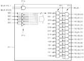
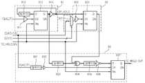
도 1은 본 발명에 따른 온칩 특성 측정 장치에 대한 블록도이다.1 is a block diagram of an on-chip characteristic measurement apparatus according to the present invention.
온칩 특성 측정 장치(2)는 테스트 대상 장치(Device Under Test, DUT)(1)에 내장되는 것으로, DUT(1)의 다른 회로들과 동일한 공정에 의해 제조되며 다른 회로들과는 별도로 존재한다.The on-chip
온칩 특성 측정 장치(2)는 발진부(21), 타이밍 검사부(22) 및 선택부(23)를 포함한다.The on-chip
발진부(21)는 입력 제어신호인 S[3:0]에 따라 다양한 주파수를 갖는 복수의 발진신호들을 출력한다. 온칩 딜레이는 발진신호를 이용하여 측정할 수 있다. 보다 상세하게 설명하면, 먼저 출력된 발진신호의 주파수로부터 제1주기를 구한다. 다음으로 제1주기와 목표값인 제2주기간의 차를 구하면 DUT(1)의 실리콘 특성에 따른 온칩 딜레이를 구할 수 있다. 여기서, 제2주기는 도시된 발진 장치(21)에 대해 SPICE 등과 같은 프로그램을 이용하여 모의실험을 수행하고, 모의실험 결과 얻어진 발진신호의 주파수로부터 제2주기를 구할 수 있다.The
타이밍 검사부(22)는 입력되는 클럭(CLK) 주파수를 기준으로 셋업/홀드(setup/hold) 시간을 검사하고, 그 결과를 성공(PASS)/실패(FAIL)를 나타내는 논리 하이/논리 로우의 TC_OUT 신호로 출력한다.The
여기서, 셋업 시간은 임의의 장치에 클럭이 도착하기 전에 데이터가 유효한 값이 되어야하는 최소 시간을 말하고, 홀드 시간은 클럭에 의해 장치가 인에이블된 후 데이터가 일정한 값을 가져야하는 최소 시간을 말한다.Here, the setup time refers to the minimum time that the data should be a valid value before the clock arrives at any device, and the hold time refers to the minimum time that the data should have a constant value after the device is enabled by the clock.
선택부(23)는 테스트 모드[1:0] 신호를 선택신호로 하여 대기상태를 나타내는 논리 로우 신호(standby logic low signal), 분압부(213)의 출력신호(RO_DIV_FO) 및 타이밍 검사부(22)의 출력신호(TC_OUT) 신호중 하나를 출력한다.The
발진부(21)는 부호화부(211), 링 발진부(212) 및 분압부(213)를 포함한다. 부호화부(211)는 입력되는 2비트의 테스트 모드 신호(테스트 모드 [1:0]) 및 4비트의 제어신호(S[3:0])를 이용하여 링 발진 패턴신호(RO_SEL[12:0])를 생성한다. 링 발진부(212)는 복수의 링 발진기들을 구비하고, 링 발진 패턴신호에 따라 인에이블(enable)되는 링 발진기를 이용하여 발진신호(RO_FO)를 출력한다. 발진 신호(RO_FO)는 GHz 단위의 주파수를 갖는다. 분압부(213)는 링 발진부(212)에서 출력되는 GHz 단위의 발진신호(RO_FO)를 측정 장비의 특성이 반영된 분주비에 따라 MHz 단위로 분주된 신호(RO_DIV_FO)를 출력한다.The
도 2는 도 1의 부호화부(211)에 대한 상세 회로도이다. 도시된 부호화부(211)는 제1논리 곱 연산기(211a), 복수의 반전기들(211b), 복수의 제2논리 곱 연산기들(211c) 및 복수의 제3논리 곱 연산기들(211d)를 포함한다.FIG. 2 is a detailed circuit diagram of the
제1논리 곱 연산기(211a)는 테스트 모드[1:0]의 비트들을 논리 곱 연산하여 RO_EN신호를 출력한다. 본 실시예에서는 테스트 모드가 '01'일 때 논리 하이 신호를 출력한다. 복수의 반전기들(211b)은 S[3:0]의 각 비트값을 반전한다.The first
제2논리 곱 연산기들(211c)는 S[3:0]의 13개의 서로 다른 비트값중 하나에 대해서만 논리 하이 신호를 출력한다. 제3논리 곱 연산기들(211c)은 제1논리 곱 연 산기(211a)의 출력과 제2논리 곱 연산기들(211b)의 출력들을 각각 논리 곱 연산하여 링 발진부(212)에 포함된 복수의 발진기들중 하나에 논리 하이의 인에이블 신호(RO_SEL[12:0])를 출력한다. 결국, RO_SEL[12:0] 신호들은 S[3:0]신호를 복호화한 것으로, 예를 들어 S[3:0]가 '0000'인 경우 RO_SEL[0]신호가 논리 하이, S[3:0]신호가 '0001'인 경우 RO_SEL[1]신호가 논리 하이가 되며, S[3:0]신호가 '1100'이면 RO_SEL[12]신호가 논리 하이가 된다.The second
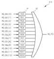
도 3은 도 1의 링 발진부(212)에 대한 상세 회로도를 도시한 것이다. 도시된 링 발진부(212)는 복수의 링 발진기들(31) 및 논리 합 연산기(32)를 포함한다.3 illustrates a detailed circuit diagram of the
링 발진기들(31)은 서로 다른 주파수의 발진 신호를 출력하고, RO_SEL[12:0] 신호에 의해 인에이블된다. 논리 합 연산기(32)는 링 발진기들(31)중 인에이블된 링 발진기에서 출력되는 발진 신호(RO_FO)를 출력한다.The ring oscillators 31 output oscillation signals of different frequencies and are enabled by the RO_SEL [12: 0] signal. The
다음 표는 도 3의 링 발진기들(31)에 대한 구성의 예를 나타낸다.The following table shows an example of the configuration for the
표 1에서 inv(Cap)은 도 4b에 도시된 커패시턴스 타입의 링 발진기인 것을 나타내고, inv(Res)는 도 4c에 도시된 저항 타입의 링 발진기인 것을 나타낸다.In Table 1, inv (Cap) represents the capacitance type ring oscillator shown in Figure 4b, inv (Res) represents the resistance type ring oscillator shown in Figure 4c.
도 4a는 도 3의 링 발진기들(31)의 회로를 도시한 것이다. 도시된 링 발진기는 직렬로 연결된 복수의 반전기들(41), RO_SEL[] 신호와 반전기들(41)중 최종 반전기의 출력을 입력으로하는 낸드 게이트(42) 그리고 낸드 게이트(42)에서 출력되는 발진 주파수를 버퍼링하는 두 반전기들(43)을 포함한다. 반전기들(41)중 최초의 반전기는 낸드 게이트(42)의 출력을 입력받는다. 스테이지(stage)의 개수는 반전기들(41)의 개수 및 낸드 게이트(42)의 합이다.FIG. 4A shows the circuit of the
RO0는 FEOL(Front End Of Line) 효과 파악을 위해 반전기(inv)들로만 구성되는 인버터 발진기이다. RO1 내지 RO5는 반전기들(41) 사이에 도 4b에 도시된 커패시턴스 패턴(capacitance pattern)을 갖는 커패시턴스 타입 링 발진기, RO6 내지 RO12는 반전기들(41) 사이에 도 4c에 도시된 레지스턴스 패턴(resistance pattern)을 갖는 레지스턴스 타입 링 발진기로 구성된다. RO0 is an inverter oscillator composed of only inverters for the front end of line (FEOL) effect. RO1 to RO5 are capacitance type ring oscillators having the capacitance pattern shown in FIG. 4B between the
M1, ..., Mn은 각각 메탈층을 나타내는 것으로, M1은 메탈층들중 가장 낮은 층을 나타낸다. 예를 들어, RO1의 경우 스테이지 수가 5개이고, 메탈 라인(line)의 길이가 500μm인 것을 나타낸다. 그 구조는 M1(500μm)-인버터(41)-M1(500μm)-인버터(41)-M1(500μm)-인버터(41)-M1(500μm)-인버터(41)-M1(500μm)-낸드 게이트(42) 순으로 연결된다.M1, ..., Mn each represent a metal layer, and M1 represents the lowest layer among the metal layers. For example, in the case of RO1, the number of stages is five, and the length of the metal line is 500 µm. The structure is M1 (500 μm)-Inverter 41-M1 (500 μm)-Inverter 41-M1 (500 μm)-Inverter 41-M1 (500 μm)-Inverter 41-M1 (500 μm)-NAND gate (42) in order.
도 4b는 커패시턴스 패턴을 도시한 것이다. 도면에서 참조번호 44는 (n-1)번째 메탈층을 나타내고 접지되며, 45 및 46은 n번째 메탈층으로 (n-1)번째 메탈층의 상부에 위치한다. 참조번호 45는 라인(46)을 감싸는 메탈이고 접지된다.4B illustrates a capacitance pattern. In the drawing,
도 4c에 레지스턴스 패턴을 도시한 것이다. 본 실시예에서 도 4b 및 4c에 도시된 커패시턴스 패턴 및 레지스턴스 패턴의 레이아웃(layout)은 라인의 폭(width)/라인이 차지하는 공간(space)을 최소화하는 설계 규칙(minimum width/space design rule for each line)에 따라 구성되었고, 각 스테이지간 간격은 5μm가 되도록 구성되었다.The resistance pattern is shown in Fig. 4C. In this embodiment, the layout of the capacitance pattern and the resistance pattern shown in FIGS. 4B and 4C is a minimum width / space design rule for each to minimize the width of the line / space that the line occupies. line), and the space between stages is 5μm.
도 4a에서 낸드 게이트(42)는 RO_SEL[] 신호에 따라 전체 링 발진기를 인에이블/디스에이블 시킨다. RO_SEL[] 신호가 논리 하이이면 낸드 게이트(42)는 반전기처럼 동작하여 링 발진기를 인에이블시키고 발진 신호를 출력한다. RO_SEL[]신호가 논리 로우이면 낸드 게이트(42)는 다른 단자의 입력에 관계없이 링 발진기를 디스에이블시킨다.In FIG. 4A, the
버퍼(43)는 낸드 게이트(42)의 출력을 버퍼링함으로써, 버퍼(43)에 연결되는 부하(미도시)에 의한 링 발진 신호의 변동을 완충한다.The
도 5는 도 1의 분압부(213)에 대한 상세 회로도를 도시한 것이다. 도시된 분압부(213)는 복수의 D 플립플롭(51)들을 포함한다.FIG. 5 is a detailed circuit diagram illustrating the
D 플립플롭(51)은 링 발진부(212)에서 출력되는 발진 신호(RO_FO)를 클럭 단자(CK)로 입력받고, 부호화부(211)에서 출력되는 RO_EN 신호를 리셋단자(RN)로 입력받아서 발진 신호(RO_FO)를 분주하여 RO_DIV_FO 신호를 출력한다. 본 실시예에서는 5 스테이지의 D 플립플롭(51)을 구비하여 32분주하지만, 측정 장비의 분해능에 따라 스테이지 수를 조절할 수 있다. 따라서 측정 장비의 특성에 무관하게 고 주파수의 링 발진신호를 분압함으로써 저속으로 동작하는 측정 장비에서 측정가능하도록 한다.The D flip-
도 6은 도 1의 타이밍 검사부(22)에 대한 상세 블록도이다. 도시된 타이밍 검사부(22)는 제1 및 제2논리 곱 연산기(51, 52), 클럭 트리 합성부(53), 셋업 타이밍 검사부(54), 홀드 타이밍 검사부(55) 및 선택부(56)를 포함한다. 또한, 타이밍 검사부(22)는 선택부(56)에서 출력되는 신호를 안정화시키기 위한 출력 안정화부(57)를 더 포함할 수 있다.6 is a detailed block diagram of the
제1논리 곱 연산기(51)는 테스트 모드[1] 및 테스트 모드[0]를 반전한 신호를 논리 곱 연산하여 셋업 타이밍 마진 검사를 위한 인에이블 신호인 TC_SETUP_EN 신호를 출력한다. 제2논리 곱 연산기(52)는 테스트 모드[1] 및 테스트 모드[0]를 논리 곱 연산하여 홀드 타이밍 마진 검사를 위한 인에이블 신호인 TC_HOLD_EN 신호를 출력한다.The first
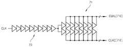
클럭 트리 합성부(53)는 입력 클럭 신호 CLK로부터 클럭 트리 합성 효과를 위한 8개의 클럭 신호들인 CLKL[7:0], CLKC[7:0]를 생성한다.The clock
도 7은 도 6의 클럭 트리 합성부(53)에 대한 상세 회로도이다. 도시된 바에 따르면, 입력 클럭 신호 CLK는 10개의 클럭 버퍼들로 구성되는 포화 로직(saturation logic)을 통해 버퍼링됨으로써 CLK의 천이 시간(transition time)을 포화시켜 CLK의 천이 시간에 관계없이 일정한 클럭 트리 신호들을 출력하게 한다. 클럭 트리부(71)는 두 가지(branch)를 포함하고 각 가지에는 8개의 클럭 버퍼들을 구비하여, 포화 로직(70)으로부터 출력된 클럭신호를 각각 딜레이시켜서 순차적으로 출력되는 8개의 클럭 신호들을 하나의 세트로 하는 CLKL[7:0], CLKC[7:0]를 출력한다.FIG. 7 is a detailed circuit diagram of the clock
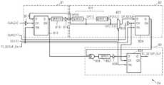
도 8은 도 6의 셋업 타이밍 검사부(54)에 대한 상세 회로도이다. 도시된 셋업 타이밍 검사부(54)는 클럭 동기 발진부(81), 펄스 생성부(82) 및 시간 위반 검사부(83)를 포함한다.FIG. 8 is a detailed circuit diagram of the
도시된 클럭 동기 발진부(81)는 CLKL[7:0]중 중간에 해당하는 CLKL[3]의 클럭 신호에 동기하는 발진 신호를 출력한다. 이에 따라 본 실시예의 셋업 타이밍 검사부(54)는 외부로부터 특정 데이터 신호의 입력이 없어도 자체적으로 신호를 생성하여 타이밍 마진을 검사할 수 있고, 클럭 신호의 라이징 에지(rising edge) 또는 폴링 에지(falling edge)에 관계없이 검사할 수 있다. 펄스 생성부(82)는 클럭 동기 발진부(81)에서 출력되는 발진 신호를 S[3:0]에 따라 소정 시간동안 지연한 펄스를 출력한다. 시간 위반 검사부(83)는 CLKL[3]의 주기보다 데이터 경로 딜레이(data path delay)가 커지면 셋업 시간이 위반되었음을 검출한다.The illustrated
클럭 동기 발진부(81)는 클럭 버퍼(811), D 플립플롭(812), 딜레이0(813) 및 반전기(84)를 포함한다. 버퍼(811)는 CLKL[3]의 신호가 안정되도록 버퍼링하여 D 플립플롭(812)의 클럭단자(CK)로 출력한다. D 플립플롭(812)의 리셋 단자(RN)는 도 6의 TC_SETUP_EN 신호를 입력받는다. D 플립플롭(812)의 출력단자(Q)는 딜레이0(813) 및 반전기(814)를 통해 다시 D 플립플롭(812)의 데이터 입력 단자(D)에 연결됨으로써, 클럭에 동기화된 발진신호를 출력한다.The
펄스 생성부(82)는 딜레이1 내지 딜레이12(821), 선택기(822), 클럭 버퍼(823) 및 D 플립플롭(824)을 포함한다.The
딜레이1 내지 딜레이12(821)는 직렬로 연결되어 클럭 동기 발진부(81)에서 출력되는 발진 신호를 순차적으로 딜레이한다. 선택기(823)는 S[3:0] 신호를 선택신호로하여 딜레이1 내지 딜레이12(821)에서 각각 딜레이된 신호중 하나를 선택하여 출력한다. 선택신호 S[3:0]는 '0000'에서 '1100'까지 순차적으로 증가하며, 그에 따라 선택기(23)에서 출력되는 데이터 경로 딜레이(DP_SETUP)도 증가하게 된다.
CLKC[7]신호는 클럭 버퍼(823)를 통해 D 플립플롭(824)의 클럭단자(CK)로 출력된다. D 플립플롭(824)은 TC_SETUP_EN 신호를 리셋단자(RN)에 입력받고, DP_SETUP 신호를 데이터 입력단자(D)에 입력받아서 버퍼(823)에서 출력되는 클럭신호에 동기하여 출력한다.The CLKC [7] signal is output to the clock terminal CK of the D flip-
시간 위반 검사부(83)는 배타적 논리 합 연산기(831), 딜레이부(832), 반전기(833) 및 D 플립플롭(834)을 포함한다.The time
배타적 논리 합 연산기(831) 및 반전기(833)는 클럭 동기 발진부(81)의 D 플립플롭(812)에서 출력되는 신호와 펄스 생성부(82)의 D 플립플롭(824)에서 출력되는 신호를 배타적 논리 합 연산하고, 반전함으로써 두 값이 동일할 경우 로직 하이를 출력한다. 이는 데이터 경로 딜레이(DP_SETUP)가 CLKL[3]의 주기보다 커지는 순간인 셋업 타임 위반(setup time violation)의 발생 여부를 알기 위한 것이다. 셋업 타임 위반은 클럭 동기 발진부(81)의 D 플립플롭(812)에서 출력되는 신호와 펄스 생성부(82)의 D 플립플롭(824)에서 출력되는 신호가 서로 다른 경우에 일어난다. 셋업 타임 위반이 일어나면, 반전기(833)는 로직 로우를 출력한다.The exclusive
여기서, 딜레이부(832)는 배타적 논리 합 연산기(831)의 출력을 캡쳐할 로직에서의 홀드 시간 위반 방지를 위해 배타적 논리 합 연산기(831)의 출력을 딜레이한다. 반전기(833)는 딜레이부(832)의 출력을 반전하여 출력한다.Here, the
본 실시예에서는 반전기(833)의 출력에 대한 글리치(glitch)를 방지하기 위하여 반전기(833)의 출력을 래치하여 TC_SETUP_OUT신호를 출력하는 D 플립플롭(834)을 더 구비한다.The present embodiment further includes a D flip-
도 9는 도 6의 홀드 타이밍 검사부(55)에 대한 상세 회로도이다. 도시된 홀드 타이밍 검사부(55)는 클럭 동기 발진부(91), 펄스 생성부(92) 및 시간 위반 검사부(93)를 포함한다.FIG. 9 is a detailed circuit diagram of the hold
클럭 동기 발진부(91)는 CLKL[7]에 동기하여 발진 신호를 출력한다. 이에 따라 본 실시예에서 홀드 타이밍 검사부(55)는 외부로부터 특정 데이터 신호의 입력이 없어도 자체적으로 신호를 생성하여 타이밍 마진을 검사할 수 있다. 펄스 생성부(92)는 발진 신호를 입력받아 CLKC[7:0] 신호중 S[3:0]에 따라 선택된 클럭 신호에 동기하여 펄스를 생성한다. 타이밍 검사부(83)는 선택된 클럭신호의 도착시간으로부터 홀드 시간 위반 여부를 검출한다.The
클럭 동기 발진부(91)는 클럭 버퍼(911), 딜레이0(912), D 플립플롭(913) 및 반전기(914)를 포함한다.The
클럭 버퍼(911)는 CLKL[7]의 신호가 안정되도록 버퍼링하여 D 플립플롭(913)의 클럭단자(CK)로 출력한다. D 플립플롭(913)의 리셋 단자는 도 6의 TC_HOLD_EN 신호를 입력받는다. D 플립플롭(913)의 출력단자(Q)는 반전기(914) 및 딜레이 0(912)를 통해 다시 D 플립플롭(913)의 데이터 입력 단자(D)에 연결됨으로써, 클럭에 동기화된 발진신호를 출력한다. The
펄스 생성부(92)는 선택기(921), 클럭 버퍼(922) 및 D 플립플롭(923)을 포함한다. 선택기는 S[3:0]을 선택신호로 하여 클럭신호 CLKC[7:0]중 하나를 선택함으로써, 다양한 지연시간(latency)을 갖는 클럭중 하나를 선택하게 된다. 즉, S[3:0] 신호를 '0000'에서 '0111'까지 증가시키면, CLKC[7:0] 신호가 순차적으로 선택된다. 그에 따라 클럭 버퍼(922)를 통해 D 플립플롭(923)의 클럭 단자(CK)에 선택된 클럭신호가 도착하는 시간이 증가하게 되어 D 플립플롭(923)이 발진신호를 제대로 캡쳐하지 못하게 되므로 홀드 시간 위반이 일어나게 된다.The
시간 위반 검사부(93)는 배타적 논리 합 연산기(934), 딜레이1,2,3(931, 933, 935), 반전기(936) 및 D 플립플롭(837)을 포함한다.The time
배타적 논리합 연산기(934) 및 반전기(936)는 펄스 생성부(92)의 D 플립플롭(923)의 출력신호와 클럭 동기 발진부(91)의 D 플립플롭(913)의 출력신호가 딜레이1(933)에 의해 소정 시간 딜레이된 신호에 대해 두 값이 동일할 경우 로직 하이를 출력함으로써 홀드 타이밍 검사가 성공했음을 알린다.The
여기서, 딜레이2(935)는 배타적 논리 합 연산기(934)의 출력을 캡쳐할 로직에서의 홀드 시간 위반 방지를 위해 배타적 논리 합 연산기(934)의 출력을 딜레이한다. 반전기(833)는 딜레이부(832)의 출력을 반전하여 출력한다.Here,
반전기(936)에서 출력되는 값에 대한 글리치를 방지하기위하여 본 실시예에서는 CLKC[7] 신호를 딜레이3(931) 및 클럭 버퍼(932)를 통해 딜레이 및 버퍼링하여 클럭 신호로 입력받고 반전기(936)의 출력을 래치하여 TC_HOLD_OUT신호로 출력하는 D 플립플롭(937)을 더 구비한다.In order to prevent the glitch on the value output from the
도 10은 도 6의 출력 안정화부(57)에 대한 상세 회로도이다. 도시된 출력 안정화부(57)는 복수의 D 플립플롭(101, 102, 103) 및 각 D 플립플롭(101, 102, 103)의 출력신호들을 논리곱 연산하는 논리곱 연산기(104)를 포함한다. D 플립플롭들(101, 102, 103)은 직렬로 연결되어 쉬프트 레지스터(shift register) 구조를 가지며, 제1플립플롭(101)은 선택부(56)의 출력신호인 TC_SOUT 신호를 입력받는다.FIG. 10 is a detailed circuit diagram of the
클럭 단자(CK)로는 CLKC[7] 신호가 입력되고, 리셋단자(RN)에는 외부로부터 리셋신호가 입력된다. 또한 각 D 플립플롭(101, 102, 103)는 홀드 시간 위반을 방지하기 위해 입력단자(D)에 딜레이1, 2 및 3(105, 106, 107)을 구비한다. 딜레이 1,2 및 3(105, 106, 107)의 딜레이 값들은 동작 조건에 따라 결정되며, 동일한 값일 수 있다.A CLKC [7] signal is input to the clock terminal CK, and a reset signal is input from the outside to the reset terminal RN. In addition, each D flip-flop (101, 102, 103) has a
논리곱 연산기(104)는 각 D 플립플롭(101, 102, 103)의 출력인 TC_SCOUT1, TC_SOUT2 및 TC_SOUT3를 논리곱 연산함으로써 셋업 또는 홀드 시간을 위반하지않으면 안정적인 로직 하이를, 셋업 또는 홀드 시간 위반시에는 안정적인 로직 로우를 출력할 수 있다.The AND
도 11(a) 내지 도 11(d)는 0.13μm 제너릭(generic) 공정에서 최하의 동작 조건하의 모의실험(simulation) 결과를 도시한 것이다. 최하의 동작조건은 NMOS/PMOS가 모두 slow/slow 상태이고, 동작 전압이 1.05V 이며, 125℃ 인 환경을 말한다.11 (a) to 11 (d) show simulation results under the lowest operating conditions in a 0.13 μm generic process. The lowest operating condition is an environment in which both NMOS / PMOS are slow / slow, the operating voltage is 1.05V, and 125 ° C.
도 11(a)는 테스트 모드가 각각 링 발진기를 이용한 딜레이 측정 모드(110), 셋업 타이밍 마진 검사 모드(111), 그리고 홀드 타이밍 마진 검사 모드(112)인 경우를 나타낸다. 도 11(b)는 각 모드(110, 111, 112)별로 제어신호 S[3:0]가 '0000'부터 '1111'까지 변하는 것을 나타낸다.FIG. 11A illustrates a case where a test mode is a
도 11(c)는 도 1의 링 발진부(212)에서 출력되는 링 발진신호를 도시한 것이다. 링 발진신호는 제어신호 S[3:0]가 '0000'에서 '1100'까지 변하는 동안 각각 발생한다. 다음 표 2는 테스트 모드가 딜레이 측정 모드(110)인 경우에 대한 트랜지스터 레벨의 모의실험 프로그램인 HSPICE를 이용한 모의실험 결과를 도시한 것이다.FIG. 11C illustrates a ring oscillation signal output from the
표 2는 S[3:0] 신호가 변함에 따라 최하, 보통 및 최상의 동작 조건에서 출력되는 발진 주파수를 나타낸다. 표 2에 따르면, 딜레이 측정 모드에서는 13가지의 링 발진 패턴에 따른 딜레이 및 커패시턴스/레지스턴스 정합성을 측정할 수 있다. 즉, 표 2에 나타난 발진 주파수의 역수를 취하면 발진 주파수의 주기를 구할 수 있고, 실제 온칩에서 측정된 주기와 모의실험에서 출력된 주기를 비교함으로써 온칩 딜레이를 알 수 있다.Table 2 shows the oscillation frequencies output at the lowest, normal and best operating conditions as the S [3: 0] signal changes. According to Table 2, in the delay measurement mode, delay and capacitance / resistance matching according to 13 ring oscillation patterns can be measured. In other words, by taking the inverse of the oscillation frequency shown in Table 2, the period of the oscillation frequency can be obtained, and the on-chip delay can be known by comparing the period measured on the actual chip with the output period in the simulation.
도 11(d)는 입력 클럭 주파수가 200 MHz일 때 타이밍 마진의 검사에 대한 TC_OUT 신호를 도시한 것이다. 타이밍 마진 검사는 S[3:0] 신호를 '0000'부터 증가시켜 가면서 TC_OUT 신호가 로직 로우가 되는 순간, 즉 타이밍 위반이 발생하는 순간을 검출한다. 셋업 타이밍 마진 검사 모드에서는 최하의 동작 조건에서 약 100MHz에서 250MHz 사이의 셋업 타이밍 마진을 검사한다. 홀드 타이밍 마진 검사 모드에서는 시스템 동작 주파수와 상관없이 홀드 타이밍 마진을 검사한다.FIG. 11 (d) shows the TC_OUT signal for checking timing margin when the input clock frequency is 200 MHz. The timing margin check increases the S [3: 0] signal from '0000' and detects the moment when the TC_OUT signal goes logic low, that is, the timing violation occurs. Setup timing margin check mode checks for setup timing margins between about 100 MHz and 250 MHz at the lowest operating conditions. In the hold timing margin check mode, the hold timing margin is checked regardless of the system operating frequency.
도시된 바에 따르면, 입력 클럭 주파수가 200MHz 이하일 때, S[3:0]신호가 '0000'에서 '0010'까지 변하는 동안 TC_OUT 신호가 로직 하이를 출력하는 것을 알 수 있다.As shown, when the input clock frequency is 200MHz or less, it can be seen that the TC_OUT signal outputs a logic high while the S [3: 0] signal is changed from '0000' to '0010'.
다음의 표 3 및 표 4는 게이트 레벨의 모의실험 프로그램인 STA(Static Timing Analysis)를 사용하여 측정한 셋업 타이밍 마진과 홀드 타이밍 마진을 각각 나타낸 것이다.Tables 3 and 4 show setup timing margins and hold timing margins respectively measured using a static timing analysis (STA), which is a gate-level simulation program.
표 3에 따르면, S[3:0] 신호가 '0000'에서 '0010'까지 변할 때, 최하의 동작 조건에서 입력 클럭 주파수가 각각 255.39, 240.30, 213.62 MHz이하일 때 TC_OUT신호가 로직 하이를 출력하고, S[3:0]신호가 '0011'이 되고 입력 클럭 주파수가 189.47MHz를 초과하면 TC_OUT신호가 로직 로우를 출력한다. 이는 도 11(d)에 도시된 결과(113)와 동일한 결과를 보여준다. 따라서, 실제 반도체 장치에서 S[3:0]이 '0011'이나 200MHz의 입력 클럭 주파수에서도 동작하였다면 200MHz~189.47MHz 만큼의 마진이 있음을 알 수 있다.According to Table 3, when the S [3: 0] signal varies from '0000' to '0010', the TC_OUT signal outputs a logic high when the input clock frequencies are below 255.39, 240.30, and 213.62 MHz, respectively, under the lowest operating conditions. When the S [3: 0] signal becomes '0011' and the input clock frequency exceeds 189.47MHz, the TC_OUT signal outputs a logic low. This shows the same result as the
표 4에서 동작 가능 마진이 양의 값인 경우에만 반도체 장치의 동작이 가능하며, 음의 값인 경우에는 동작하지 않는다. 즉, 그만큼 마진이 부족하다는 것을 의미한다. 예를 들어, S[3:0]이 '0100'일 때, 동작 가능 마진은 -0.059ns로 게이트 레벨에서는 마진이 부족하지만, 도 11(d)의 참조번호 114의 경우에는 TC_OUT 신호가 로직 하이이다. 이는 트랜지스터 레벨 모의실험에서는 동작가능하지만 게이트 레벨 모의실험에서는 동작하지 않는 것을 뜻하며, 트랜지스터 레벨의 모의실험과 비교하여 게이트 레벨의 모의실험 결과에 게이트 레벨 추상화(Abstraction)에 따른 모의실험 마진(Simulation Margin)이 나타난 결과이다.In Table 4, the semiconductor device can be operated only when the operational margin is a positive value, and it does not operate when the operating margin is negative. That means that the margin is not enough. For example, when S [3: 0] is '0100', the operational margin is -0.059 ns and the margin is insufficient at the gate level. However, in the case of
본 발명에 대해 상기 실시예를 참고하여 설명하였으나, 이는 예시적인 것에 불과하며, 본 발명에 속하는 기술 분야의 통상의 지식을 가진 자라면 이로부터 다양한 변형 및 균등한 타 실시예가 가능하다는 점을 이해할 것이다. 따라서 본 발명의 진정한 기술적 보호범위는 첨부된 특허청구범위의 기술적 사상에 의해 정해져야할 것이다.Although the present invention has been described with reference to the above embodiments, it is merely illustrative, and those skilled in the art will understand that various modifications and equivalent other embodiments are possible therefrom. . Therefore, the true technical protection scope of the present invention will be defined by the technical spirit of the appended claims.
본 발명에 따르면, ASIC/SOC 설계시 실리콘 메인 칩 상태를 반영할 수 있는 온칩 딜레이 및 타이밍 마진을 측정할 수 있다. 또한 온칩 딜레이 및 타이밍 마진 측정함으로써 반도체 집적회로 설계를 위한 보다 정확한 공정 관리 및 효과적인 실리콘 결함(silicon failure) 분석이 가능하다.According to the present invention, the on-chip delay and timing margin can be measured to reflect the silicon main chip state in the ASIC / SOC design. On-chip delay and timing margin measurements also enable more accurate process control and effective silicon failure analysis for semiconductor integrated circuit designs.
Claims (36)
Translated fromKoreanPriority Applications (3)
| Application Number | Priority Date | Filing Date | Title |
|---|---|---|---|
| KR1020050094641AKR100801054B1 (en) | 2005-10-08 | 2005-10-08 | Timing margin measuring device of semiconductor circuit and on-chip characteristic measuring device including same |
| US11/416,374US7408371B2 (en) | 2005-10-08 | 2006-05-02 | Apparatus for measuring on-chip characteristics in semiconductor circuits and related methods |
| JP2006271818AJP2007108172A (en) | 2005-10-08 | 2006-10-03 | Apparatus for measuring on-chip characteristics of semiconductor circuits and method related thereto |
Applications Claiming Priority (1)
| Application Number | Priority Date | Filing Date | Title |
|---|---|---|---|
| KR1020050094641AKR100801054B1 (en) | 2005-10-08 | 2005-10-08 | Timing margin measuring device of semiconductor circuit and on-chip characteristic measuring device including same |
Publications (2)
| Publication Number | Publication Date |
|---|---|
| KR20070039416A KR20070039416A (en) | 2007-04-12 |
| KR100801054B1true KR100801054B1 (en) | 2008-02-04 |
Family
ID=37910544
Family Applications (1)
| Application Number | Title | Priority Date | Filing Date |
|---|---|---|---|
| KR1020050094641AExpired - Fee RelatedKR100801054B1 (en) | 2005-10-08 | 2005-10-08 | Timing margin measuring device of semiconductor circuit and on-chip characteristic measuring device including same |
Country Status (3)
| Country | Link |
|---|---|
| US (1) | US7408371B2 (en) |
| JP (1) | JP2007108172A (en) |
| KR (1) | KR100801054B1 (en) |
Cited By (1)
| Publication number | Priority date | Publication date | Assignee | Title |
|---|---|---|---|---|
| US12210059B2 (en) | 2021-05-27 | 2025-01-28 | Samsung Electronics Co., Ltd. | Test element group and test method |
Families Citing this family (15)
| Publication number | Priority date | Publication date | Assignee | Title |
|---|---|---|---|---|
| KR100746177B1 (en)* | 2005-07-26 | 2007-08-03 | 삼성전자주식회사 | Effective transmission verification circuit and semiconductor device including the same |
| US7755403B2 (en)* | 2006-11-14 | 2010-07-13 | Hynix Semiconductor Inc. | Apparatus and method of setting operation mode in DLL circuit |
| US7973549B2 (en)* | 2007-06-12 | 2011-07-05 | International Business Machines Corporation | Method and apparatus for calibrating internal pulses in an integrated circuit |
| KR100956782B1 (en)* | 2008-09-24 | 2010-05-12 | 주식회사 하이닉스반도체 | Setup / hold time test device and method |
| EP2382711A4 (en) | 2009-01-27 | 2013-10-09 | Agere Systems Inc | Critical-path circuit for performance monitoring |
| US8089296B2 (en)* | 2009-06-23 | 2012-01-03 | International Business Machines Corporation | On-chip measurement of signals |
| KR101069377B1 (en)* | 2009-07-29 | 2011-09-30 | 연세대학교 산학협력단 | Inverting Amplifiers and Inverting Amplifier-Based Systems |
| KR101094903B1 (en) | 2009-07-30 | 2011-12-15 | 주식회사 하이닉스반도체 | Test device of semiconductor integrated circuit |
| US8504456B2 (en)* | 2009-12-01 | 2013-08-06 | Bank Of America Corporation | Behavioral baseline scoring and risk scoring |
| JP2011216536A (en)* | 2010-03-31 | 2011-10-27 | Consortium For Advanced Semiconductor Materials & Related Technologies | Test circuit for semiconductor integrated circuits |
| US9122891B2 (en)* | 2013-08-12 | 2015-09-01 | Microsoft Technology Licensing, Llc | Functional timing sensors |
| JP2018078357A (en)* | 2016-11-07 | 2018-05-17 | ソニー株式会社 | Semiconductor integrated circuit and control method of semiconductor integrated circuit |
| CN113884865B (en)* | 2020-07-01 | 2023-12-01 | 复旦大学 | Test circuit and test method of D trigger |
| WO2022041154A1 (en)* | 2020-08-28 | 2022-03-03 | 华为技术有限公司 | Hold time margin detection circuit |
| KR20240052470A (en)* | 2022-10-14 | 2024-04-23 | 삼성전자주식회사 | Teg circuit, semiconductor device, and test method of the teg circuit |
Citations (2)
| Publication number | Priority date | Publication date | Assignee | Title |
|---|---|---|---|---|
| KR20010076307A (en)* | 2000-01-18 | 2001-08-11 | 오우라 히로시 | Method and apparatus for testing semiconductor devices |
| KR20070019480A (en)* | 2005-08-12 | 2007-02-15 | 삼성전자주식회사 | Semiconductor memory device and test system thereof |
Family Cites Families (8)
| Publication number | Priority date | Publication date | Assignee | Title |
|---|---|---|---|---|
| JPH0770573B2 (en)* | 1989-07-11 | 1995-07-31 | 富士通株式会社 | Semiconductor integrated circuit device |
| GB9417244D0 (en)* | 1994-08-26 | 1994-10-19 | Inmos Ltd | Integrated circuit device and test method therefor |
| US6466520B1 (en)* | 1996-09-17 | 2002-10-15 | Xilinx, Inc. | Built-in AC self test using pulse generators |
| DE10018190C2 (en)* | 1999-05-18 | 2003-04-17 | Ibm | Switch seamlessly between two oscillator precision clocks |
| KR100754238B1 (en) | 2000-03-24 | 2007-09-03 | 톰슨 라이센싱 에스.에이. | Oscillator Devices for Controllable and Testable Integrated Circuits |
| US6952790B2 (en)* | 2001-03-30 | 2005-10-04 | Intel Corporation | System for varying timing between source and data signals in a source synchronous interface |
| JP2004132824A (en) | 2002-10-10 | 2004-04-30 | Toshiba Corp | LSI chip delay measurement mechanism |
| KR100590204B1 (en)* | 2003-11-04 | 2006-06-15 | 삼성전자주식회사 | Integrated circuit device with on-chip setup / hold measurement circuit |
- 2005
- 2005-10-08KRKR1020050094641Apatent/KR100801054B1/ennot_activeExpired - Fee Related
- 2006
- 2006-05-02USUS11/416,374patent/US7408371B2/ennot_activeExpired - Fee Related
- 2006-10-03JPJP2006271818Apatent/JP2007108172A/enactivePending
Patent Citations (2)
| Publication number | Priority date | Publication date | Assignee | Title |
|---|---|---|---|---|
| KR20010076307A (en)* | 2000-01-18 | 2001-08-11 | 오우라 히로시 | Method and apparatus for testing semiconductor devices |
| KR20070019480A (en)* | 2005-08-12 | 2007-02-15 | 삼성전자주식회사 | Semiconductor memory device and test system thereof |
Cited By (1)
| Publication number | Priority date | Publication date | Assignee | Title |
|---|---|---|---|---|
| US12210059B2 (en) | 2021-05-27 | 2025-01-28 | Samsung Electronics Co., Ltd. | Test element group and test method |
Also Published As
| Publication number | Publication date |
|---|---|
| US7408371B2 (en) | 2008-08-05 |
| JP2007108172A (en) | 2007-04-26 |
| US20070080701A1 (en) | 2007-04-12 |
| KR20070039416A (en) | 2007-04-12 |
Similar Documents
| Publication | Publication Date | Title |
|---|---|---|
| US7408371B2 (en) | Apparatus for measuring on-chip characteristics in semiconductor circuits and related methods | |
| US8736338B2 (en) | High precision single edge capture and delay measurement circuit | |
| US6473476B1 (en) | Method and apparatus for providing deterministic resets for clock divider systems | |
| US8907681B2 (en) | Timing skew characterization apparatus and method | |
| Pei et al. | A high-precision on-chip path delay measurement architecture | |
| JP4874963B2 (en) | Synchronization between low and high frequency digital signals | |
| Polzer et al. | An approach for efficient metastability characterization of FPGAs through the designer | |
| Beer et al. | Metastability challenges for 65nm and beyond; simulation and measurements | |
| Abas et al. | Built-in time measurement circuits–a comparative design study | |
| Nedovic et al. | A test circuit for measurement of clocked storage element characteristics | |
| JP4846128B2 (en) | Semiconductor device and test method thereof | |
| US8797082B2 (en) | Apparatus and methods for clock characterization | |
| US7228515B2 (en) | Methods and apparatuses for validating AC I/O loopback tests using delay modeling in RTL simulation | |
| US20220209759A1 (en) | Clock sweeping system | |
| Beer et al. | A new 65nm LP metastability measurment test circuit | |
| KR100752657B1 (en) | Test apparatus and test method for testing memory access time using PLL | |
| JP3202722B2 (en) | Operation speed evaluation circuit and method for clock synchronous circuit | |
| US6891403B2 (en) | On-chip PLL locked frequency determination method and system | |
| Zhihong et al. | Self-calibrate two-step digital setup/hold time measurement | |
| US11764763B1 (en) | Method and apparatus for in-situ on-chip timing | |
| US6989696B2 (en) | System and method for synchronizing divide-by counters | |
| WO2024148502A1 (en) | Circuitry for staggering capture clocks in testing electronic circuits with multiple clock domains | |
| Wei et al. | A Novel All-Digital on-Chip Aging Sensor Robust to Process Variations | |
| Omaña et al. | Low-cost on-chip clock jitter measurement scheme | |
| JP2001228213A (en) | Semiconductor integrated circuit device and method for inspecting clock skew |
Legal Events
| Date | Code | Title | Description |
|---|---|---|---|
| A201 | Request for examination | ||
| PA0109 | Patent application | St.27 status event code:A-0-1-A10-A12-nap-PA0109 | |
| PA0201 | Request for examination | St.27 status event code:A-1-2-D10-D11-exm-PA0201 | |
| E902 | Notification of reason for refusal | ||
| PE0902 | Notice of grounds for rejection | St.27 status event code:A-1-2-D10-D21-exm-PE0902 | |
| P11-X000 | Amendment of application requested | St.27 status event code:A-2-2-P10-P11-nap-X000 | |
| P13-X000 | Application amended | St.27 status event code:A-2-2-P10-P13-nap-X000 | |
| PG1501 | Laying open of application | St.27 status event code:A-1-1-Q10-Q12-nap-PG1501 | |
| E902 | Notification of reason for refusal | ||
| PE0902 | Notice of grounds for rejection | St.27 status event code:A-1-2-D10-D21-exm-PE0902 | |
| P11-X000 | Amendment of application requested | St.27 status event code:A-2-2-P10-P11-nap-X000 | |
| P13-X000 | Application amended | St.27 status event code:A-2-2-P10-P13-nap-X000 | |
| E701 | Decision to grant or registration of patent right | ||
| PE0701 | Decision of registration | St.27 status event code:A-1-2-D10-D22-exm-PE0701 | |
| GRNT | Written decision to grant | ||
| PR0701 | Registration of establishment | St.27 status event code:A-2-4-F10-F11-exm-PR0701 | |
| PR1002 | Payment of registration fee | St.27 status event code:A-2-2-U10-U11-oth-PR1002 Fee payment year number:1 | |
| PG1601 | Publication of registration | St.27 status event code:A-4-4-Q10-Q13-nap-PG1601 | |
| PR1001 | Payment of annual fee | St.27 status event code:A-4-4-U10-U11-oth-PR1001 Fee payment year number:4 | |
| PR1001 | Payment of annual fee | St.27 status event code:A-4-4-U10-U11-oth-PR1001 Fee payment year number:5 | |
| R18-X000 | Changes to party contact information recorded | St.27 status event code:A-5-5-R10-R18-oth-X000 | |
| FPAY | Annual fee payment | Payment date:20130102 Year of fee payment:6 | |
| PR1001 | Payment of annual fee | St.27 status event code:A-4-4-U10-U11-oth-PR1001 Fee payment year number:6 | |
| FPAY | Annual fee payment | Payment date:20140103 Year of fee payment:7 | |
| PR1001 | Payment of annual fee | St.27 status event code:A-4-4-U10-U11-oth-PR1001 Fee payment year number:7 | |
| FPAY | Annual fee payment | Payment date:20141231 Year of fee payment:8 | |
| PR1001 | Payment of annual fee | St.27 status event code:A-4-4-U10-U11-oth-PR1001 Fee payment year number:8 | |
| FPAY | Annual fee payment | Payment date:20160104 Year of fee payment:9 | |
| PR1001 | Payment of annual fee | St.27 status event code:A-4-4-U10-U11-oth-PR1001 Fee payment year number:9 | |
| FPAY | Annual fee payment | Payment date:20170102 Year of fee payment:10 | |
| PR1001 | Payment of annual fee | St.27 status event code:A-4-4-U10-U11-oth-PR1001 Fee payment year number:10 | |
| PR1001 | Payment of annual fee | St.27 status event code:A-4-4-U10-U11-oth-PR1001 Fee payment year number:11 | |
| PR1001 | Payment of annual fee | St.27 status event code:A-4-4-U10-U11-oth-PR1001 Fee payment year number:12 | |
| PC1903 | Unpaid annual fee | St.27 status event code:A-4-4-U10-U13-oth-PC1903 Not in force date:20200130 Payment event data comment text:Termination Category : DEFAULT_OF_REGISTRATION_FEE | |
| PC1903 | Unpaid annual fee | St.27 status event code:N-4-6-H10-H13-oth-PC1903 Ip right cessation event data comment text:Termination Category : DEFAULT_OF_REGISTRATION_FEE Not in force date:20200130 |