Movatterモバイル変換


[0]ホーム

URL:


KR100800468B1 - Hardware encryption / decryption device and method for low power high speed operation - Google Patents

Hardware encryption / decryption device and method for low power high speed operation
Download PDF

Info

Publication number
KR100800468B1
KR100800468B1KR1020040005647AKR20040005647AKR100800468B1KR 100800468 B1KR100800468 B1KR 100800468B1KR 1020040005647 AKR1020040005647 AKR 1020040005647AKR 20040005647 AKR20040005647 AKR 20040005647AKR 100800468 B1KR100800468 B1KR 100800468B1
Authority
KR
South Korea
Prior art keywords
data
result
inverse
bit
field
Prior art date
Legal status (The legal status is an assumption and is not a legal conclusion. Google has not performed a legal analysis and makes no representation as to the accuracy of the status listed.)
Expired - Fee Related
Application number
KR1020040005647A
Other languages
Korean (ko)
Other versions
KR20050078271A (en
Inventor
안경문
노미정
Original Assignee
삼성전자주식회사
Priority date (The priority date is an assumption and is not a legal conclusion. Google has not performed a legal analysis and makes no representation as to the accuracy of the date listed.)
Filing date
Publication date
Application filed by 삼성전자주식회사filedCritical삼성전자주식회사
Priority to KR1020040005647ApriorityCriticalpatent/KR100800468B1/en
Priority to US11/024,855prioritypatent/US20050169463A1/en
Priority to JP2005022279Aprioritypatent/JP2005215688A/en
Priority to DE200510005335prioritypatent/DE102005005335A1/en
Publication of KR20050078271ApublicationCriticalpatent/KR20050078271A/en
Application grantedgrantedCritical
Publication of KR100800468B1publicationCriticalpatent/KR100800468B1/en
Anticipated expirationlegal-statusCritical
Expired - Fee Relatedlegal-statusCriticalCurrent

Links

Images

Classifications

Landscapes

Abstract

Translated fromKorean

저전력 고속 동작을 위한 하드웨어 암호화/복호화 장치 및 그 방법이 개시된다. 상기 하드웨어 암호화/복호화 장치는, 라운드 연산부에서 각 라운드 연산에 해당하는 키들을 입력받아, 입력 데이터를 암호문으로 변환한다. 상기 하드웨어 암호화/복호화 장치의 S-BOX 연산 또는 역 S-BOX 연산은, 갈로아 필드 GF(28) 상의 원소를 갈로아 필드 GF(((22)2)2) 상의 원소로 변환한 뒤 합성 필드(Composite field)를 이용하여 원소의 곱셈의 역원을 계산하고, 상기 계산 결과를 이용하여 입력받는 벡터를 다른 벡터로 치환한다.An apparatus and method for hardware encryption / decryption for low power high speed operation are disclosed. The hardware encryption / decryption apparatus receives a key corresponding to each round operation from a round operation unit and converts the input data into a cipher text. The S-BOX operation or the inverse S-BOX operation of the hardware encryption / decryption apparatus converts an element on Galloa field GF (28 ) into an element on Galloa field GF (((22 )2 )2 ). The inverse of the multiplication of elements is calculated using a composite field, and the input vector is replaced with another vector using the calculation result.

Description

Translated fromKorean
저전력 고속 동작을 위한 하드웨어 암호화/복호화 장치 및 그 방법{Hardware cryptographic engine and method improving power consumption and operation speed}Hardware cryptographic engine and method improving power consumption and operation speed for low power high speed operation

본 발명의 상세한 설명에서 인용되는 도면을 보다 충분히 이해하기 위하여 각 도면의 간단한 설명이 제공된다.BRIEF DESCRIPTION OF THE DRAWINGS In order to better understand the drawings cited in the detailed description of the invention, a brief description of each drawing is provided.

도 1은 본 발명의 일실시예에 따른 하드웨어 암호화 장치의 블록도이다.1 is a block diagram of a hardware encryption apparatus according to an embodiment of the present invention.

도 2는 도 1의 제1 라운드(120) 내지 제9 라운드(140)를 나타내는 구체적인 블록도이다.FIG. 2 is a detailed block diagram illustrating thefirst round 120 to theninth round 140 of FIG. 1.

도 3은 도 1의 제10 라운드(150)를 나타내는 구체적인 블록도이다.3 is a detailed block diagram illustrating thetenth round 150 of FIG. 1.

도 4는 도 1의 키들을 발생시키는 키 스케쥴러를 나타내는 블록도이다.4 is a block diagram illustrating a key scheduler for generating the keys of FIG. 1.

도 5는 도 2 및 도 3의 Sub_Byte 회로(160)에서 사용되는 S-BOX를 나타내는 블록도이다.5 is a block diagram illustrating an S-BOX used in theSub_Byte circuit 160 of FIGS. 2 and 3.

도 6은 GF(((22)2)2) 상에서 역원 계산을 위한 도 5의 역원 계산부(162)를 나타내는 구체적인 블록도이다.FIG. 6 is a detailed block diagram illustrating the inverse calculatingunit 162 of FIG. 5 for inverse calculating on GF (((22 )2 )2 ).

도 7은 GF((22)2) 상에서 역원 계산을 위한 도 6의 제1 역원 계산기(605)를 나타내는 구체적인 블록도이다.FIG. 7 is a specific block diagram illustrating the firstinverse calculator 605 of FIG. 6 for inverse calculation on GF ((22 )2 ).

도 8은 GF((22)2) 상에서 승산을 위한 도 6의 4비트 승산기(602, 606, 607)를 나타내는 구체적인 블록도이다.FIG. 8 is a detailed block diagram illustrating the 4-bit multipliers 602, 606, 607 of FIG. 6 for multiplication on GF ((22 )2 ).

도 9는 GF(22) 상에서 승산을 위한 도 7 및 도 8의 2비트 승산기(702, 707, 708, 803, 804, 805)를 나타내는 구체적인 블록도이다.9 is a specific block diagram illustrating the 2-bit multipliers 702, 707, 708, 803, 804, and 805 of FIGS. 7 and 8 for multiplication on GF 22 .

도 10은 도 1의 하드웨어 암호화 장치로부터 전송된 암호문을 복호하는 하드웨어 복호화 장치를 나타내는 일례이다.FIG. 10 is an example of a hardware decryption apparatus that decrypts a cipher text transmitted from the hardware encryption apparatus of FIG. 1.

도 11은 도 10의 복호 과정에 있는 제10 라운드 내지 제2 라운드(1200~1400)를 나타내는 구체적인 블록도이다.FIG. 11 is a detailed block diagram illustrating tenth tosecond rounds 1200 to 1400 in the decoding process of FIG. 10.

도 12는 도 10의 제1 라운드(1500)를 나타내는 구체적인 블록도이다.FIG. 12 is a detailed block diagram illustrating thefirst round 1500 of FIG. 10.

도 13은 도 11 및 도 12의 역 Sub_Byte 회로(1700, 2100)에서 사용되는 역 S-BOX를 나타내는 블록도이다.FIG. 13 is a block diagram illustrating an inverse S-BOX used in theinverse Sub_Byte circuits 1700 and 2100 of FIGS. 11 and 12.

본 발명은 하드웨어 암호화/복호화 장치(cryptographic engine)에 관한 것으로, 특히 AES(Advanced Encryption Standard) 알고리즘의 하드웨어 암호화 또는 복호화 장치에 관한 것이다.The present invention relates to a hardware encryption / decryption apparatus, and more particularly, to a hardware encryption or decryption apparatus of an advanced encryption standard (AES) algorithm.

오늘날 스마트 카드, IC(Integrated Circuit) 카드 등을 통한 통신이나 인터넷 통신, 무선 랜(LAN) 통신 등에서, 유저(user)가 전송하는 정보에는 보안이 유지 되어야 하는 비빌 정보가 상당히 많이 존재한다. 따라서, 유저의 비밀 정보가 해킹(hacking)에 의하여 유출되는 것을 방지하기 위하여, 서명이나 인증 절차를 밟아 전송되는 비밀 정보를 암호문으로 만들어 전송하는 하드웨어 암호화/복호화 장치가 필요하다.Today, in the communication through smart cards, integrated circuit (IC) cards, Internet communication, wireless LAN (LAN) communication, and the like, there is a great deal of information about the security of the user. Therefore, in order to prevent the user's confidential information from being leaked by hacking, a hardware encryption / decryption apparatus that encrypts and transmits secret information transmitted through a signature or authentication procedure is required.

암호화(encryption) 연산은 일반적으로 속도가 느리기 때문에, 스마트 카드와 같은 적용에서 하드웨어로 구현하는 경우가 많다. RSA(Rivest-Shamir-Adelman), ECC 체계(Elliptic Curve Crypto System) 등과 같은 공개키 알고리즘 뿐만 아니라 DES(Data Encryption Standard), AES(Advanced Encryption Standard)와 같은 대칭키 알고리즘도 하드웨어로 구현된다.Encryption operations are generally slow, so they are often implemented in hardware in applications such as smart cards. In addition to public key algorithms such as Rivest-Shamir-Adelman (RSA) and Elliptic Curve Crypto System (ECC), symmetric key algorithms such as Data Encryption Standard (DES) and Advanced Encryption Standard (AES) are implemented in hardware.

특히, AES는 SPN(Substitution Permutation Network) 구조를 가지고, 이는 DES를 대치하는 대칭키 암호화 알고리즘으로써, 블록의 길이는 128비트이고, 키(Key) 길이는 128, 192, 및 256 비트를 사용한다. 사용되는 키 길이 각각에 따라 10, 12, 및 14 라운드를 수행한다. AES의 암호화 과정은, 초기 입력키 합산 및 각 라운드의 연산으로 이루어진다. 예를 들어, AES에서 암호화 과정시 사용되는 라운드 수를 Nr이라 하면, "Sub_Byte 변환(transformation)", "Shift_Row 변환", "Mix_Column 변환", 및 "Add_Round_Key 연산"으로 이루어진 라운드 연산이 (Nr-1)번 수행되고, 최종 라운드 연산에서는 "Mix_Column 변환"을 제외한 "Sub_Byte 변환", "Shift_Row 변환", 및 "Add_Round_Key 연산"이 1번 수행된다. 따라서, 종래의 AES 암호화 알고리즘의 구현에서, 암호화 과정에는 (Nr+1) 이상의 클럭 싸이클이 요구되고, 암호화 과정의 역과정을 수행하는 복호화(decryption) 과정에는 2(Nr+1) 이상의 클럭 싸이클이 요구된다. 이와 같은 AES 암호화 알고리즘의 라운드 연산에 대하여 미국 공개 특허, "US2003-0133568" 또는 한국 공개 특허, "KR2002-61718"에 잘 나타나 있다.In particular, AES has a Substitution Permutation Network (SPN) structure, which is a symmetric key encryption algorithm that replaces DES, and has a block length of 128 bits and a key length of 128, 192, and 256 bits. Perform 10, 12, and 14 rounds depending on each key length used. The encryption process of AES consists of adding up the initial input key and calculating each round. For example, if the number of rounds used in the encryption process in AES is Nr, a round operation consisting of "Sub_Byte transformation", "Shift_Row transformation", "Mix_Column transformation", and "Add_Round_Key operation" is performed (Nr-1). ), And in the final round operation, "Sub_Byte conversion", "Shift_Row conversion", and "Add_Round_Key operation" are performed once except for "Mix_Column conversion". Therefore, in the implementation of the conventional AES encryption algorithm, a clock cycle of (Nr + 1) or more is required for the encryption process, and a clock cycle of 2 (Nr + 1) or more is required for the decryption process that performs the reverse process of the encryption process. Required. The round operation of such an AES encryption algorithm is well described in US published patent, "US2003-0133568" or Korean published patent, "KR2002-61718".

그런데, 비선형(non-linear) 변환인 "Sub_Byte 변환"은 S-BOX에 의하여 이루어지고, S-BOX의 연산은 AES 구현 시 가장 많은 전력을 소모한다. 즉, S-BOX는 비선형 변환 함수로써 입력 데이터를 다른 데이터로 치환하고, 이때, 비선형 변환 함수의 연산을 위하여 사용되는 메모리와 회로의 복잡도가 커서 많은 전력을 소모한다. 예를 들어, S-BOX에서 비선형 함수에 따른 치환 연산의 수행을 위하여, 룩업 테이블(Look-up Table), SOP(Sum-of-Products), POS(Produce-of-Sum), PPRM(Positive Polarity Reed-Muller) form, BDD(Binary Decision Diagram) 등 다양한 방법들이 적용된다. S-BOX의 입력값에 대한 변환값을 얻기 위하여, 룩업 테이블(Look-up Table) 방식은 ROM(Read Only Memory)에 그 값들을 저장하여 참조한다. SOP, POS, PPRM form, BDD 등의 방식은 데이터들을 8개의 입력에 의한 이진(binary) 표현으로 나타내어 회로를 구현한다. 이때, 이러한 종래의 방식으로 S-BOX를 구현하면, 800~2200개 정도의 게이트(gate) 사이즈가 요구되어, 스마트 카드, IC 카드 등과 같이 메모리 및 대역폭에 제한이 있고, 저전력 및 빠른 처리 속도가 요구되는 소형 시스템에 적합하지 않다는 문제점이 있다.By the way, non-linear conversion "Sub_Byte conversion" is performed by the S-BOX, the operation of the S-BOX consumes the most power when implementing AES. In other words, the S-BOX is a nonlinear conversion function and replaces the input data with other data. At this time, the memory and the circuit complexity used for the operation of the nonlinear conversion function are large and consume a lot of power. For example, look-up tables, sum-of-products, produce-of-sum, and positive polarity are performed to perform substitution operations based on nonlinear functions in S-BOX. Various methods such as Reed-Muller form and BDD (Binary Decision Diagram) are applied. In order to obtain a conversion value for the input value of the S-BOX, the look-up table method stores and references the values in a read only memory (ROM). The SOP, POS, PPRM form, BDD, etc. represent the data in binary representation by eight inputs to implement the circuit. At this time, if the S-BOX is implemented in such a conventional manner, a gate size of about 800 to 2200 is required, and there is a limitation in memory and bandwidth, such as a smart card and an IC card, and low power and fast processing speed There is a problem that it is not suitable for the small system required.

따라서, 본 발명이 이루고자하는 기술적 과제는, 스마트 카드나 IC 카드 등 소형 시스템에 용이하게 적용할 수 있는 저전력 및 고속의 암호화 또는 복호화가 가능한 하드웨어 암호화/복호화 장치를 제공하는 데 있다.Accordingly, an object of the present invention is to provide a hardware encryption / decryption apparatus capable of low power and high speed encryption or decryption that can be easily applied to a small system such as a smart card or an IC card.

본 발명이 이루고자하는 다른 기술적 과제는, 저전력 및 고속의 암호화 또는 복호화가 가능한 하드웨어 암호화/복호화 방법을 제공하는 데 있다.Another object of the present invention is to provide a hardware encryption / decryption method capable of low power and high speed encryption or decryption.

상기의 기술적 과제를 달성하기 위한 본 발명에 따른 하드웨어 암호화/복호화 장치는, 라운드 연산부,및 키 스케쥴러를 구비하는 것을 특징으로 한다. 상기 라운드 연산부는 각 라운드에 해당하는 N개의 키들을 입력받아, 제1 라운드에서 상기 키들 중 제1 키를 이용하여 입력 데이터를 암호문으로 변환하고, 나머지 N-1 라운드 각각에서 순차적으로 상기 키들 중 제2 키 내지 제N 키를 이용하여 이전 라운드의 변환 결과를 다른 암호문으로 변환한다. 상기 키 스케쥴러는 입력키를 이용하여 상기 제1 키 내지 상기 제N 키 각각을 생성한다. 상기 라운드 각각의 S-BOX은, 갈로아 필드 GF(28) 상의 원소를 갈로아 필드 GF(((22)2)2) 상의 원소로 변환한 뒤 합성 필드(Composite)를 이용하여 원소의 곱셈의 역원을 계산하고, 상기 계산 결과를 이용하여 입력받는 벡터를 다른 벡터로 치환하는 것을 특징으로 한다. 상기 하드웨어 암호화/복호화 장치는, 전송할 데이터와 상기 입력키를 합산하여, 그 합산 결과를 상기 입력 데이터로서 출력하는 합산기를 더 구비하는 것을 특징으로 한다.Hardware encryption / decryption apparatus according to the present invention for achieving the above technical problem is characterized in that it comprises a round operation unit, and a key scheduler. The round operation unit receives N keys corresponding to each round, converts the input data into cipher text using the first of the keys in the first round, and sequentially performs the first of the keys in each of the remaining N-1 rounds. The conversion result of the previous round is converted into another ciphertext using the 2nd to Nth keys. The key scheduler generates each of the first to Nth keys using an input key. Each S-BOX of the round converts an element on Galloa field GF (28 ) to an element on Galloa field GF (((22 )2 )2 ) and then uses a composite field to The inverse of the multiplication is calculated, and the input vector is replaced with another vector using the calculation result. The hardware encryption / decryption apparatus may further include a summer that adds the data to be transmitted and the input key and outputs the sum result as the input data.

상기 S-BOX는, 델타 변환부, 역원 계산부, 역 델타 변환부, 및 아핀 변환부를 구비하는 것을 특징으로 한다. 상기 델타 변환부는 입력받는 벡터의 각 원소를 이루는 갈로아 필드 GF(28) 상의 원소를 갈로아 필드 GF(((22)2)2) 상의 원소로 변환 한다. 상기 역원 계산부는 상기 갈로아 필드 GF(((22)2)2) 상의 원소의 역원을 계산하여 출력한다. 상기 역 델타 변환부는 상기 갈로아 필드 GF(((22)2)2) 상의 원소의 역원을 갈로아 필드 GF(28) 상의 원소로 변환한다. 상기 아핀 변환부는 아핀 함수에 따라 상기 변환된 갈로아 필드 GF(28) 상의 원소를 아핀 변환한다.The S-BOX includes a delta converter, an inverse calculator, an inverted delta converter, and an affine converter. The delta converter converts an element on galoa field GF (28 ) constituting each element of the input vector into an element on galoa field GF (((22 )2 )2 ). The inverse calculating unit calculates and outputs an inverse of an element on the galoa field GF (((22 )2 )2 ). The inverse delta converter converts the inverse of the element on the Galloa field GF (((22 )2 )2 ) to an element on the Galloa field GF (28 ). The affine transformation unit affines an element on the transformed Galloa field GF (28 ) according to an affine function.

상기의 기술적 과제를 달성하기 위한 본 발명에 따른 하드웨어 암호화/복호화 방법은, N개의 라운드들에 대응하는 해당 N개의 키들을 입력받는 단계; 상기 라운드들 중 제1 라운드에서 상기 키들 중 제1 키를 이용하여 입력 데이터를 암호문으로 변환하는 단계; 나머지 N-1 라운드들 각각에서 순차적으로 상기 키들 중 제2 키 내지 제N 키를 이용하여 이전 라운드의 변환 결과를 다른 암호문으로 변환하는 단계; 및 입력키를 이용하여 상기 제1 키 내지 상기 제N 키 각각을 생성하는 단계를 구비하고, 상기 라운드들 각각의 암호문으로 변환 단계는, S-BOX 연산에서, 갈로아 필드 GF(28) 상의 원소를 갈로아 필드 GF(((22)2)2) 상의 원소로 변환한 뒤 합성 필드(Composite)를 이용하여 원소의 곱셈의 역원을 계산하고, 입력받는 벡터를 상기 계산 결과를 이용하여 다른 벡터로 치환하는 단계를 구비하는 것을 특징으로 한다. 상기 하드웨어 암호화/복호화 방법은, 전송할 데이터와 상기 입력키를 합산하여, 그 합산 결과를 상기 입력 데이터로서 출력하는 단계를 더 구비하는 것을 특징으로 한다.According to another aspect of the present invention, there is provided a hardware encryption / decryption method comprising: receiving corresponding N keys corresponding to N rounds; Converting input data into a cipher text using a first key of the keys in a first round of the rounds; Converting the conversion result of the previous round into another ciphertext using the second to Nth keys of the keys sequentially in each of the remaining N-1 rounds; And generating each of the first key to the Nth key using an input key, and converting the ciphertext into each round of the rounds in the S-BOX operation on the Gallo field GF 28 . After converting an element to an element on Galoa field GF (((22 )2 )2 ), calculate the inverse of the multiplication of the elements using the composite field and convert the input vector to another using the result of the calculation. And a step of replacing with a vector. The hardware encryption / decryption method may further include summing data to be transmitted and the input key and outputting the sum result as the input data.

본 발명과 본 발명의 동작상의 이점 및 본 발명의 실시에 의하여 달성되는 목적을 충분히 이해하기 위해서는 본 발명의 바람직한 실시예를 예시하는 첨부 도 면 및 첨부 도면에 기재된 내용을 참조하여야만 한다.In order to fully understand the present invention, the operational advantages of the present invention, and the objects achieved by the practice of the present invention, reference should be made to the accompanying drawings which illustrate preferred embodiments of the present invention and the contents described in the accompanying drawings.

이하, 첨부한 도면을 참조하여 본 발명의 바람직한 실시예를 설명함으로써, 본 발명을 상세히 설명한다. 각 도면에 제시된 동일한 참조부호는 동일한 부재를 나타낸다.Hereinafter, exemplary embodiments of the present invention will be described in detail with reference to the accompanying drawings. Like reference numerals in the drawings denote like elements.

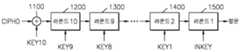
도 1은 본 발명의 일실시예에 따른 하드웨어 암호화 장치(100)의 블록도이다. 도 1을 참조하면, 본 발명의 일실시예에 따른 AES 방식의 하드웨어 암호화 장치(100)는, 합산기(110), 및 라운드 연산을 수행하는 다수의 N개의 라운드들(120~150)을 구비한다. 이외에도, 상기 하드웨어 암호화 장치(100)는, 도 4에 도시된 바와 같은 키 스케쥴러(key scheduler)(400)를 구비한다. 상기 키 스케쥴러(400)는 입력키(INKEY)와 상기 다수의 N개 라운드들(120~150)에 해당키들(KEY1~KEY10)을 제공한다. 상기 키 스케쥴러(400)에 대해서는 도 4의 설명에서 좀더 자세히 설명된다. 상기 다수의 N개 라운드들(120~150) 각각에서의 라운드 연산은, 각 라운드에서 중복되는 연산이 공유될 수 있다.1 is a block diagram of ahardware encryption apparatus 100 according to an embodiment of the present invention. Referring to FIG. 1, an AEShardware encryption apparatus 100 according to an embodiment of the present invention includes asummer 110 and a plurality ofN rounds 120 to 150 performing round operations. do. In addition, thehardware encryption apparatus 100 includes akey scheduler 400 as illustrated in FIG. 4. Thekey scheduler 400 provides an input key (INKEY) and corresponding keys (KEY1 to KEY10) for the plurality of N rounds (120 to 150). Thekey scheduler 400 is described in more detail in the description of FIG. 4. Round operations in each of theN rounds 120 to 150 may be shared with each other.

상기 합산기(110)는 초기 입력키(INKEY) 합산을 수행한다. 즉, 상기 합산기(110)는 전송할 데이터(TXD)와 상기 입력키(INKEY)를 합산하여, 그 합산 결과를 라운드들(120~150) 중 제1 라운드(120)의 입력 데이터로서 출력한다. 여기서, 전송할 데이터(TXD)의 블록 길이는, 일반적인 경우와 마찬가지로 128 비트인 것으로 가정된다.Thesummer 110 performs initial input key (INKEY) summing. That is, thesummer 110 adds the data TXD and the input key INKEY, and outputs the sum result as input data of thefirst round 120 among therounds 120 to 150. Here, it is assumed that the block length of the data TXD to be transmitted is 128 bits as in the general case.

상기 다수의 N개 라운드들(120~150)은 각 라운드에 해당하는 N개의 키들(KEY1~KEY10)을 입력받아, 암호화를 위한 라운드 연산을 수행한다. 여기서, 키 들(KEY1~KEY10) 각각의 데이터 길이는 128 비트인 것으로 가정하고, 이에 따라 라운드들(120~150)의 수는 10개이고 10 라운드 연산을 수행하는 것으로 가정된다. 이외에도, 주지된 바와 같이, 키 길이가 192, 및 256 비트 각각인 경우에는 12 및 14 라운드 연산을 수행한다.The plurality of N rounds 120 to 150 receive N keys KEY1 to KEY10 corresponding to each round and perform a round operation for encryption. Here, it is assumed that the data length of each of the keys KEY1 to KEY10 is 128 bits. Accordingly, it is assumed that the number ofrounds 120 to 150 is 10 and 10 round operations are performed. In addition, as is well known, when the key length is 192 and 256 bits, respectively, 12 and 14 round operations are performed.

상기 라운드들(120~150) 중 제1 라운드(120)는 상기 키들 중 제1 키(KEY1)를 이용하여 입력 데이터(TXD + INKEY)를 암호문으로 변환한다. 이에 따라, 나머지 9 라운드들(130~150) 각각은 순차적으로 상기 키들 중 제2 키(KEY2) 내지 제10 키(KEY10)를 이용하여 이전 라운드의 변환 결과를 다른 암호문으로 변환한다. 제10번째 최종 라운드(150)는 제10 키(KEY10)를 이용하여 제9 라운드(140)의 변환 결과를 최종 암호문(CIPHD)으로 변환한다. 이와 같이 전송할 데이터(TXD)가 암호화된 최종 암호문(CIPHD)은 스마트 카드, IC(Integrated Circuit) 카드 등과 같은 소형 시스템에서 전송되는 비빌 정보가 된다. 이외에도 상기 AES 방식의 하드웨어 암호화/복호화 장치는 보안이 유지되어야 하는 비빌 정보의 송수신을 위하여, 인터넷 통신, 무선 랜(LAN) 통신 등에도 이용될 수 있다.Thefirst round 120 of therounds 120 to 150 converts the input data TXD + INKEY into a cipher text by using the first key KEY1 among the keys. Accordingly, each of the remaining ninerounds 130 to 150 sequentially converts the conversion result of the previous round into another ciphertext using the second key KEY2 to the tenth key KEY10 among the keys. The tenthfinal round 150 converts the conversion result of theninth round 140 to the final ciphertext CIPHD using the tenth key KEY10. The final ciphertext (CIPHD) in which the data TXD is encrypted as described above becomes biblio information transmitted from a small system such as a smart card or an integrated circuit (IC) card. In addition, the AES-type hardware encryption / decryption apparatus may be used for internet communication, wireless LAN (LAN) communication, and the like, for transmission and reception of security information to be maintained.

여기서, 상기 라운드들(120~150)에 의하여, 일반적인 AES 암호화 과정과 마찬가지로, 라운드 수가 10이므로, "Sub_Byte 변환(transformation)", "Shift_Row 변환", "Mix_Column 변환", 및 "Add_Round_Key 연산"으로 이루어진 라운드 연산이 9번 수행되고, 최종 라운드 연산에서는 "Mix_Column 변환"을 제외한 "Sub_Byte 변환", "Shift_Row 변환", 및 "Add_Round_Key 연산"이 1번 수행된다. 일반적으로, 비선형(non-linear) 변환인 "Sub_Byte 변환"을 수행하기 위해서는 사용되는 메모리와 회로의 복잡도가 커서 많은 전력을 소모한다. 이에 따라, 본 발명의 일실시예에 따른 하드웨어 암호화/복호화 장치는, 라운드 연산에서 Sub_Byte 회로(도 2의 160, 도 3의 200) 또는 역 Sub_Byte 회로(도 11의 1700, 도 12의 2100)에 새로운 S-BOX(도 5 및 도 13)를 구비하여, 종래와 다른 방식으로 "Sub_Byte 변환"과 "역 Sub_Byte 변환"을 수행하여 입력받는 벡터를 다른 벡터로 치환한다. 먼저, 본 발명의 일실시예에 따라 제안된 하드웨어 암호화 장치(100)에서는, 상기 라운드들(120~150)의 라운드 연산 수행 시 S-BOX(도 5)의 하드웨어 부담을 줄이고 소비 전력을 줄이기 위하여, "Sub_Byte 변환"의 수행에서 갈로아 필드(Galois Field) GF(28) 상의 원소의 곱셈의 역원 계산(multiplicative inverse)이 갈로아 필드 GF(2)의 합성 필드(composite field)들, 즉, GF(22), GF((22)2), 및 GF(((22)2)2) 상의 연산으로 이루어진다. 곱셈의 역원은 곱하여 1로 만드는 수로서 역수(reciprocal number)이다. 본 발명의 일실시예에 따라 제안된 S-BOX(도 5)의 동작에 대해서는 도 2, 도 3, 및 도 5의 설명에서 좀더 구체적으로 기술된다.Here, therounds 120 to 150 have a number of rounds of 10, as in the general AES encryption process, and thus are composed of "Sub_Byte transformation", "Shift_Row transformation", "Mix_Column transformation", and "Add_Round_Key operation". The round operation is performed nine times, and in the final round operation, "Sub_Byte conversion", "Shift_Row conversion", and "Add_Round_Key operation" are performed once except for "Mix_Column conversion". In general, in order to perform a "sub_byte conversion", which is a non-linear conversion, the memory and circuit complexity used are large and consume a lot of power. Accordingly, the hardware encryption / decryption apparatus according to an embodiment of the present invention may be applied to the Sub_Byte circuit (160 in FIG. 2 and 200 in FIG. 3) or the reverse Sub_Byte circuit (1700 in FIG. 11 and 2100 in FIG. 12) in a round operation. With a new S-BOX (FIGS. 5 and 13), "Sub_Byte Conversion" and "Inverse Sub_Byte Conversion" are performed in a manner different from that of the prior art to replace the received vector with another vector. First, in thehardware encryption apparatus 100 proposed according to an embodiment of the present invention, in order to reduce hardware burden and power consumption of the S-BOX (FIG. 5) when performing round operations of therounds 120 to 150. , The multiplicative inverse of the multiplication of the elements on the Galois field GF (28 ) in the performance of the "Sub_Byte conversion" is the composite fields of the Gallois field GF (2), i.e. Operations on GF (22 ), GF ((22 )2 ), and GF (((22 )2 )2 ). The inverse of the multiplication is the number by which to multiply to one, the reciprocal number. The operation of the proposed S-BOX (FIG. 5) according to an embodiment of the present invention will be described in more detail in the description of FIGS. 2, 3, and 5.

도 2는 도 1의 제1 라운드(120) 내지 제9 라운드(140)를 나타내는 구체적인 블록도이다. 도 2를 참조하면, 제1 라운드(120) 내지 제9 라운드(140) 각각은, Sub_Byte 회로(160), Shift_Row 회로(170), Mix_Column 회로(180), 및 합산기(190)를 구비한다. 위에서 기술한 바와 같이, 라운드 수가 10이므로, 상기 제1 라운드(120) 내지 상기 제9 라운드(140)를 통하여, "Sub_Byte 변환(transformation)", "Shift_Row 변환", "Mix_Column 변환", 및 "Add_Round_Key 연산"으로 이루어진 라운드 연산이 9번 수행된다.FIG. 2 is a detailed block diagram illustrating thefirst round 120 to theninth round 140 of FIG. 1. Referring to FIG. 2, each of thefirst rounds 120 toninth rounds 140 includes aSub_Byte circuit 160, aShift_Row circuit 170, aMix_Column circuit 180, and asummer 190. As described above, since the number of rounds is 10, the "Sub_Byte transformation", "Shift_Row transformation", "Mix_Column transformation", and "Add_Round_Key" are performed through thefirst round 120 through theninth round 140. Operation is performed nine times.

상기 Sub_Byte 회로(160)는, S-BOX(도 5)를 통하여, "Sub_Byte 변환(transformation)"을 위한 갈로아 필드 GF(28) 상의 역원 계산에서, 갈로아 필드 GF(((22)2)2) 상의 연산을 이용하여 계산하고, 상기 계산 결과를 이용하여 입력받는 벡터(INCIPH)를 다른 벡터로 치환한다. 즉, 갈로아 필드(Galois Field) GF(28) 상의 역원 계산은 갈로아 필드 GF(2)의 합성 필드들, 즉, GF(22), GF((22)2), 및 GF(((22)2)2) 상의 연산으로 이루어진다.TheSub_Byte circuit 160, via an S-BOX (FIG. 5), calculates the inverse source on the Galoa field GF (28 ) for "Sub_Byte transformation", the Galloa field GF (((22 )).2 ) The calculation is performed using the operations of2 ), and the input vector INCIPH is replaced with another vector using the calculation result. In other words, the inverse calculations on Galois Field GF (28 ) are performed on synthetic fields of Galoa Field GF (2), ie GF (22 ), GF ((22 )2 ), and GF ( ((22 )2 )2 )

이와 같은 합성 필드를 이용하여 역원을 계산하는 이론에 대해서는, 논문, "Akashi Satoh, Sumio Morioka, Kohji Takano, and Seiji Munetoh, <A Compact Rijndael Hardware Architecture with S-Box Optimization>, ASIACRYPT 2001"이 참조되었다. 일반적인 통신 표준에 따르면, 갈로아 필드 GF(28), GF(22), GF((22)2), 및 GF(((22)2)2) 각각에 대한 원시 다항식(primitive polynomial)은 [수학식 1]과 같다. [수학식 1]과 같은 원시 다항식은 약분될 수 없는 기약 다항식(irreducible polynomial)이다. λ={1100}2∈ GF((22)2)이고, ø={10}2 ∈ GF(22)이다. 즉, 제1 계수 λ는 갈로아 필드 GF((22)2) 상에서 이진수 {1100}2이고, 제2 계수 ø는 갈로아 필드 GF(22) 상에서 이진수 {10}2이다.For the theory of calculating inverses using such synthetic fields, the paper, "Akashi Satoh, Sumio Morioka, Kohji Takano, and Seiji Munetoh, <A Compact Rijndael Hardware Architecture with S-Box Optimization>, ASIACRYPT 2001", was referenced. . According to general communication standards, primitive polynomials for each of Galoa field GF (28 ), GF (22 ), GF ((22 )2 ), and GF (((22 )2 )2 ) ) Is the same as [Equation 1]. Primitive polynomials such asEquation 1 are irreducible polynomials that cannot be abbreviated. λ = {1100}2 μs GF ((22 )2 ) and ø = {10}2 μs GF (22 ). That is, the first coefficient λ is binary {1100}2 on galloa field GF ((22 )2 ) and the second coefficient ø is binary {10}2 on galloa field GF (22 ).

[수학식 1][Equation 1]

Figure 112004003632697-pat00001

상기 Shift_Row 회로(170)는 "Shift_Row 변환"을 수행하기 위하여, 상기 Sub_Byte 회로(160)의 출력 신호를 입력 벡터로 받아, 로우 단위로 쉬프트 처리하는 함수에 따라 상기 입력 벡터를 로우 단위로 쉬프트 처리하여 출력한다. 상기 Mix_Column 회로(180)는 "Mix_Column 변환"을 수행하기 위하여, 컬럼 단위로 치환 처리하는 함수에 따라 상기 Shift_Row 회로(170)의 출력 벡터를 컬럼 단위로 치환 처리하여 출력한다. 상기 합산기(190)는 "Add_Round_Key 연산"을 수행하기 위하여, 상기 Mix_Column 회로(180)의 출력 벡터와 상기 키들 중 해당 라운드 키(KEYN)를 합산하여 출력한다. 상기 합산기(190)에서 출력된 암호문(OUTCIPH)은 다음 라운드 의 입력이 된다.Theshift_row circuit 170 receives the output signal of thesub_byte circuit 160 as an input vector and shifts the input vector in row units according to a function of shift processing in row units in order to perform "shift_row conversion". Output In order to perform "Mix_Column conversion", theMix_Column circuit 180 substitutes and outputs the output vector of theShift_Row circuit 170 by a column according to a function of performing a per-column substitution. Thesummer 190 sums and outputs the output vector of theMix_Column circuit 180 and the corresponding round key KEYN of the keys in order to perform an "Add_Round_Key operation". The ciphertext OUTCIPH output from thesummer 190 becomes the next round of input.

도 3은 도 1의 제10 라운드(150)를 나타내는 구체적인 블록도이다. 도 3을 참조하면, 도 1의 제10 라운드(150)는 Sub_Byte 회로(200), Shift_Row 회로(210), 및 합산기(220)를 구비한다. 위에서 기술한 바와 같이, 라운드 수가 10이므로, 최 종 라운드인 상기 제10 라운드(150)를 통하여, "Sub_Byte 변환(transformation)", "Shift_Row 변환", 및 "Add_Round_Key 연산"으로 이루어진 라운드 연산이 1번 수행된다. 상기 Sub_Byte 회로(200), 상기 Shift_Row 회로(210), 및 상기 합산기(220)의 동작은 도 2의 Sub_Byte 회로(160), Shift_Row 회로(170), 및 합산기(190)의 동작과 같으므로 여기서는 설명을 생략한다.3 is a detailed block diagram illustrating thetenth round 150 of FIG. 1. Referring to FIG. 3, thetenth round 150 of FIG. 1 includes aSub_Byte circuit 200, aShift_Row circuit 210, and asummer 220. As described above, since the number of rounds is 10, the round operation consisting of "Sub_Byte transformation", "Shift_Row transformation", and "Add_Round_Key operation" is performed once through thetenth round 150, which is the last round. Is performed. Since the operation of theSub_Byte circuit 200, theShift_Row circuit 210, and thesummer 220 is the same as that of theSub_Byte circuit 160, theShift_Row circuit 170, and thesummer 190 of FIG. 2. The description is omitted here.

도 4는 도 1의 키들(INKEY, KEY1~KEY10)을 발생시키는 키 스케쥴러(400)를 나타내는 블록도이다. 도 4를 참조하면, 상기 키 스케쥴러(400)는 레지스터(410), 먹스(multiplexer)(420), 및 키 생성기(key generator)(430)를 구비한다.FIG. 4 is a block diagram illustrating akey scheduler 400 generating the keys INKEY and KEY1 to KEY10 of FIG. 1. Referring to FIG. 4, thekey scheduler 400 includes aregister 410, amultiplexer 420, and akey generator 430.

도 4에서, 입력키(INKEY)는 유저가 암호화에 사용하는 키로서, 본 발명에 따른 AES 암호화 과정을 위하여 유저에 의하여 입력되는 키이다. 상기 키 생성기(430)는 상기 먹스(420)를 통하여 입력되는 상기 입력키(INKEY)를 이용하여 상기 제1 라운드(120)에서 사용될 제1 키(KEY1)를 생성한다. 상기 키 스케쥴러(400)는 제1 라운드(120)의 연산이 이루어지기 전인 초기에, 도 1의 합산기(110)에 상기 입력키(INKEY)를 제공한다. 도 1의 합산기(110)에 상기 입력키(INKEY)의 제공과 상기 키 생성기(430)에서의 상기 제1 키(KEY1)의 발생은 시스템 클럭(미도시)의 한 싸이클에 이루어질 수 있다. 상기 키 생성기(430)에서 생성된 상기 제1 키(KEY1)는 상기 레지스터(410)에 저장되고 동시에 제1 라운드(120)의 라운드 키가되며, 다음 시스템 클럭에 상기 레지스터(410)로부터 상기 먹스(420)로 입력된다. 상기 먹스(420)는 상기 소정 제어 신호(RNDST)의 논리 상태에 따라, 선택적으로 입력키(INKEY) 또는 상기 레지스터(410)에서 출력된 상기 제1 키(KEY1)를 출력한다. 상기 제1 키(KEY1)가 상기 키 생성기(430)의 입력이 되면, 상기 키 생성기(430)는 제2 키(KEY2)를 생성하여 출력한다.In FIG. 4, an INKEY is a key used by the user for encryption and is a key input by the user for the AES encryption process according to the present invention. Thekey generator 430 generates a first key KEY1 to be used in thefirst round 120 by using the input key INKEY input through themux 420. Thekey scheduler 400 initially provides the input key INKEY to thesummer 110 of FIG. 1 before the operation of thefirst round 120 is performed. Provision of the input key INKEY to thesummer 110 of FIG. 1 and generation of the first key KEY1 in thekey generator 430 may be performed in one cycle of a system clock (not shown). The first key KEY1 generated by thekey generator 430 is stored in theregister 410 and simultaneously becomes a round key of thefirst round 120, and the mux from theregister 410 on the next system clock. Inputted to 420. Themux 420 selectively outputs an input key INKEY or the first key KEY1 output from theregister 410 according to a logic state of the predetermined control signal RNDST. When the first key KEY1 is input to thekey generator 430, thekey generator 430 generates and outputs a second key KEY2.

즉, 나머지 9 라운드들(130~150) 각각에서 사용될 제2 키(KEY2) 내지 제10 키(KEY10)는, 상기 키 생성기(430)가 이전 라운드에서 사용되는 키(KEYN)가 저장되는 상기 레지스터(410)의 값을 이용하여 순차적으로 발생시킨다. 예를 들어, 상기 제1 키(KEY1)가 상기 레지스터(410)로부터 상기 먹스(420)를 통하여 상기 키 생성기(430)에 입력될 때, 상기 키 생성기(430)는 상기 제1 키(KEY1)를 이용하여 제2 라운드(130)에서 사용될 제2 키(KEY2)를 발생시킨다.That is, the second key KEY2 to the tenth key KEY10 to be used in each of the remaining ninerounds 130 to 150 are the registers in which thekey generator 430 stores the key KEYN used in the previous round. It generates them sequentially using the value of 410. For example, when the first key KEY1 is input to thekey generator 430 from theregister 410 through themux 420, thekey generator 430 may be configured to enter the first key KEY1. To generate a second key KEY2 to be used in thesecond round 130.

이와 같이 상기 키 스케쥴러(400)가 입력키(INKEY)를 이용하여 상기 제1 키(KEY1) 내지 상기 제10 키(KEY10) 각각을 생성함으써, 10개 라운드들(120~150)에 해당 라운드키들(KEY1~KEY10)을 제공한다. 위에서 기술한 바와 같이, 도 1의 합산기(110)에 상기 입력키(INKEY)의 제공과 상기 제1 키(KEY1)의 발생은 시스템 클럭의 한 싸이클에 이루어지므로, 도 1과 같은 본 발명에 따른 AES 암호화 알고리즘의 구현에서, 암호화 과정에는 10 클럭 싸이클이 요구된다. 암호화 과정의 역과정을 수행하는 복호화 과정에는 20 클럭 싸이클이 요구된다. 이와 같이, 본 발명의 AES 암호화 과정에서는 키 발생 클럭 싸이클 수를 최소화하여 빠른 연산이 이루어지도록 하였다. 복호화 과정에 관하여는 도 10 내지 도 13의 설명에서 좀 더 구체적으로 설명된다.As such, thekey scheduler 400 generates each of the first key KEY1 to the tenth key KEY10 by using an input key INKEY, thereby corresponding to tenrounds 120 to 150. Provide keys KEY1 to KEY10. As described above, the provision of the input key INKEY to thesummer 110 of FIG. 1 and the generation of the first key KEY1 are performed in one cycle of the system clock, and thus, the present invention as shown in FIG. In the implementation of the AES encryption algorithm according to the above, the encryption process requires 10 clock cycles. 20 clock cycles are required for the decryption process, which performs the reverse process of the encryption process. As described above, in the AES encryption process of the present invention, the number of key generation clock cycles is minimized so that fast operation is performed. The decoding process will be described in more detail in the description of FIGS. 10 to 13.

도 5는 도 2 및 도 3의 Sub_Byte 회로(160, 200)에서 사용되는 S-BOX를 나타내는 블록도이다. 도 5를 참조하면, 상기 S-BOX는 델타 변환부(δ:isomorphic transformation unit)(161), 역원 계산부(inverse operation unit)(162), 역 델타 변환부(δ-1:inverse isomorphic transformation unit)(163), 및 아핀 변환부(affine transformation unit)(164)를 구비한다.5 is a block diagram illustrating an S-BOX used in theSub_Byte circuits 160 and 200 of FIGS. 2 and 3. Referring to FIG. 5, the S-BOX includes a delta transform unit δ, aninverse operation unit 162, and an inverse isomorphictransformation unit δ−1. 163 and anaffine transformation unit 164.

상기 델타 변환부(161)는 입력받는 벡터(SBIN)의 각 원소를 이루는 갈로아 필드 GF(28) 상의 원소를 갈로아 필드 GF(((22)2)2) 상의 원소로 동형 변환(isomorphic transformation)한다. 도 5에 도시된 바와 같이, 입력받는 벡터(SBIN)는 128 비트이고, 이들은 8 비트의 데이터를 가지는 16 원소들(S00~S33)로 이루어진다. 상기 델타 변환부(161)의 동형 변환(isomorphic transformation) 식은 [수학식 2] 및 [수학식 3]과 같다. [수학식 2]에서, x는 입력 벡터(SBIN)이고, y는 동형 변환(isomorphic transformation) 벡터 δ에 의하여 변환된 벡터이다.Thedelta converter 161 converts an element on the Galloa field GF (28 ) constituting each element of the input vector SBIN to an element on the Galloa field GF (((22 )2 )2 ). isomorphic transformation). As shown in FIG. 5, the input vector SBIN is 128 bits, and these are composed of 16 elements S00 to S33 having 8 bits of data. The isomorphic transformation formula of thedelta transformation unit 161 is the same as [Equation 2] and [Equation 3]. In Equation 2, x is an input vector (SBIN), and y is a vector transformed by an isomorphic transformation vector δ.

[수학식 2][Equation 2]

y=δ*xy = δ * x

[수학식 3][Equation 3]

Figure 112004003632697-pat00002

상기 역원 계산부(162)는 상기 갈로아 필드 GF(((22)2)2) 상의 원소의 곱셈의 역원을 계산하여 출력한다. 상기 역원 계산부(162)의 역원 계산은 도 6에서 자세히 설명된다.Theinverse calculating unit 162 calculates and outputs an inverse of the multiplication of elements on the galoa field GF (((22 )2 )2 ). The inverse calculation of theinverse calculation unit 162 is described in detail with reference to FIG. 6.

상기 역 델타 변환부(163)는 상기 역원 계산부(162)에서 계산된 상기 갈로아 필드 GF(((22)2)2) 상의 원소의 곱셈의 역원을 갈로아 필드 GF(28) 상의 원소로 역 동형 변환(inverse isomorphictransformation)한다. 상기 역 델타 변환부(163)의 역 동형 변환(inverse isomorphic transformation) 식은 [수학식 4] 및 [수학식 5]와 같다. [수학식 4]에서, y는 상기 역 델타 변환부(163)가 입력받는 역원 벡터이고, x는 역 동형 변환(inverse isomorphic transformation) 벡터 δ-1에 의하여 역 변환된 벡터이다.The inversedelta conversion unit 163 calculates the inverse of the multiplication of the elements on the Galoa field GF (((22 )2 )2 ) calculated by theinverse calculating unit 162 on the Galoa field GF (28 ). Inverse isomorphic transformation with elements. The inverse isomorphic transformation formula of the inversedelta transformation unit 163 is the same as [Equation 4] and [Equation 5]. In Equation 4, y is an inverse vector received by the inversedelta transform unit 163 and x is a vector inversely transformed by an inverse isomorphic transformation vector δ−1 .

[수학식 4][Equation 4]

x=δ-1*yx = δ-1 * y

[수학식 5][Equation 5]

Figure 112004003632697-pat00003

상기 아핀 변환부(164)는 아핀 함수에 따라 상기 역 델타 변환부(163)에서 변환된 갈로아 필드 GF(28) 상의 원소를 아핀 변환한다. 도 5에 도시된 바와 같이, 아핀 변환된 벡터(SBOUT)는 상기 델타 변환부(161)가 입력받는 벡터(SBIN)와 마찬가지로 128 비트이고, 이들은 8 비트의 데이터를 가지는 16 원소들(S00'~S33')로 이루어진다. 아핀 변환 식은 [수학식 6]과 같다. [수학식 6]에서 x0~x7은 상기 역 델타 변환부(163)에서 변환된 갈로아 필드 GF(28) 상의 원소(8비트 데이터)의 비트 값이고, x'0~x'7은 아핀 변환된 원소(8비트 데이터)의 비트 값이다.Theaffine transforming unit 164 affines the elements on the galoa field GF 28 converted by the inversedelta transforming unit 163 according to an affine function. As shown in FIG. 5, the affine transformed vector SBOUT is 128 bits like the vector SBIN input by thedelta converter 161, and these are 16 elements S00 ′ to 8 bits of data. S33 '). The affine transformation formula is shown in [Equation 6]. In Equation 6, x0 to x7 are bit values of elements (8-bit data) on the Galoa field GF (28 ) converted by the inversedelta conversion unit 163, and x '0 to x'7 Is the bit value of the affine transformed element (8-bit data).

[수학식 6][Equation 6]

Figure 112004003632697-pat00004

도 6은 GF(((22)2)2) 상에서 역원 계산을 위한 도 5의 역원 계산부(162)를 나타내는 구체적인 블록도이다. 도 6을 참조하면, 상기 역원 계산부(162)는 제1 합산기(601), 제1 승산기(602), 제1 자승기(603), 제1 계수 승산기(608), 제2 합산기(604), 제1 역원 계산기(605), 제2 승산기(606), 및 제3 승산기(607)를 구비한다. 상기 제1 합산기(601)는 상기 갈로아 필드 GF(((22)2)2) 상의 원소를 이루는 8비트 디지털 데이터의 하위 4비트 데이터 PL[3:0]과 상위 4비트 데이터 PH[3:0]를 제1 합산한다. 상기 제1 승산기(602)는 갈로아 필드 GF((22)2) 상에서 상기 제1 합산 결과에 상기 하위 4비트 데이터 PL[3:0]를 제1 승산한다. 상기 제1 자승기(603)는 상기 상위 4비트 데이터 PH[3:0]를 제1 자승(square)한다. 상기 제1 계수 승산기(608)는 상기 제1 자승 결과에 제1 계수(λ)([수학식 1] 참조)를 승산한다. 상기 제2 합산기(604)는 상기 제1 승산 결과와 상기 제1 자승 결과를 제2 합산한 다. 상기 제1 역원 계산기(605)는 상기 갈로아 필드 GF((22)2) 상에서 상기 제2 합산 결과의 역원을 계산한다. 상기 제1 역원 계산기(605)의 역원 계산에 대해서는 도 7의 설명에서 자세히 기술된다.FIG. 6 is a detailed block diagram illustrating theinverse calculating unit 162 of FIG. 5 for inverse calculating on GF (((22 )2 )2 ). Referring to FIG. 6, theinverse calculation unit 162 may include afirst summer 601, afirst multiplier 602, afirst square 603, afirst coefficient multiplier 608, and a second summer ( 604, a firstinverse calculator 605, asecond multiplier 606, and athird multiplier 607. Thefirst summer 601 is a lower 4-bit data PL [3: 0] and an upper 4-bit data P of 8-bit digital data forming an element on the Galoa field GF (((22 )2 )2 ). First addH [3: 0]. Thefirst multiplier 602 first multiplies the lower 4-bit data PL [3: 0] by the first sum result on Galoa field GF ((22 )2 ). The first square 603 first squares the upper four bit data PH [3: 0]. Thefirst coefficient multiplier 608 multiplies the first square result by a first coefficient λ (see Equation 1). Thesecond summer 604 second sums the first multiplication result and the first square result. The firstinverse calculator 605 calculates the inverse of the second sum result on the Galoa field GF ((22 )2 ). The inverse calculation of the firstinverse calculator 605 is described in detail in the description of FIG. 7.

상기 제2 승산기(606)는 갈로아 필드 GF((22)2) 상에서 상기 제2 합산 결과의 역원에 상기 제1 합산 결과를 제2 승산하여, 상기 제2 승산 결과를 상기 하위 4비트 데이터의 역원 PL-1[3:0]으로서 출력한다. 상기 제3 승산기(607)는 갈로아 필드 GF((22)2) 상에서 상기 제2 합산 결과의 역원에 상기 상위 4비트 데이터 PH[3:0]를 제3 승산하여, 상기 제3 승산 결과를 상기 상위 4비트 데이터의 역원 PH-1[3:0]으로서 출력한다.Thesecond multiplier 606 second multiplies the first sum result by a second inverse of the second sum result on Galoa field GF ((22 )2 ) to multiply the second multiply result by the lower four-bit data. Output as the inverse of PL-1 [3: 0]. Thethird multiplier 607 third multiplies the upper four-bit data PH [3: 0] by a third inverse of the second sum result on Galoa field GF ((22 )2 ), thereby performing the third multiplication. The result is output as the inverse PH-1 [3: 0] of the upper 4-bit data.

도 7은 GF((22)2) 상에서 역원 계산을 위한 도 6의 제1 역원 계산기(605)를 나타내는 구체적인 블록도이다. 도 7을 참조하면, 도 6의 제1 역원 계산기(605)는 제3 합산기(701), 제4 승산기(702), 제2 자승기(703), 제2 계수 승산기(704), 제4 합산기(705), 제2 역원 계산기(706), 제5 승산기(707), 및 제6 승산기(708)를 구비한다. 상기 제3 합산기(701)는 도 6의 제2 합산기(604)에서 출력되는 제2 합산 결과를 이루는 4비트 디지털 데이터의 하위 2비트 데이터 QL[1:0]와 상위 2비트 데이터 QH[1:0]를 제3 합산한다. 상기 제4 승산기(702)는 갈로아 필드 GF(22) 상에서 상 기 제3 합산 결과에 상기 하위 2비트 데이터 QL[1:0]를 제4 승산한다. 상기 제2 자승기(703)는 상기 상위 2비트 데이터 QH[1:0]를 제2 자승한다. 상기 제2 계수 승산기(704)는 상기 제2 자승 결과에 제2 계수(ø)([수학식 1] 참조)를 승산한다. 상기 제4 합산기(705)는 상기 제4 승산 결과와 상기 제2 계수 승산 결과를 제4 합산한다. 상기 제2 역원 계산기(706)는 상기 제4 합산 결과의 자승(square)을 계산하여 상기 제4 합산 결과의 역원으로서 출력한다. 즉, 상기 제4 합산 결과의 자승은 그 역원과 같다. 상기 제5 승산기(707)는 갈로아 필드 GF(22) 상에서 상기 제4 합산 결과의 역원에 상기 제3 합산 결과를 제5 승산하여, 상기 제5 승산 결과를 상기 하위 2비트 데이터의 역원 QL-1[1:0]으로서 출력한다. 상기 제6 승산기(708)는 상기 갈로아 필드 GF(22) 상에서 상기 제4 합산 결과의 역원에 상기 상위 2비트 데이터를 제6 승산하여, 상기 제6 승산 결과를 상기 상위 2비트 데이터의 역원 QH-1[1:0]으로서 출력한다.FIG. 7 is a specific block diagram illustrating the firstinverse calculator 605 of FIG. 6 for inverse calculation on GF ((22 )2 ). Referring to FIG. 7, the firstinverse calculator 605 of FIG. 6 includes athird summer 701, afourth multiplier 702, a secondsquare multiplier 703, asecond coefficient multiplier 704, and a fourth. Asummer 705, a secondinverse calculator 706, afifth multiplier 707, and asixth multiplier 708. Thethird summer 701 is the lower two-bit data QL [1: 0] and the upper two-bit data Q of the 4-bit digital data forming the second sum result output from thesecond summer 604 of FIG. 6. Third addH [1: 0]. Thefourth multiplier 702 multiplies the lower two-bit data QL [1: 0] by a fourth multiplication result on the Galoa field GF 22 . The second squarer 703 second-squares the upper two-bit data QH [1: 0]. Thesecond coefficient multiplier 704 multiplies the second square result by a second coefficient ø (see [Equation 1]). Thefourth summer 705 fourth sums the fourth multiplication result and the second coefficient multiplication result. The secondinverse calculator 706 calculates a square of the fourth sum result and outputs the square of the fourth sum result. That is, the square of the fourth summation result is the same as the inverse. Thefifth multiplier 707 multiplies the third sum result by the fifth sum of the inverses of the fourth sum result on Galoa field GF (22 ), and multiplies the fifth multiplication result by the inverse Q of the lower two-bit data. Output asL-1 [1: 0]. Thesixth multiplier 708 multiplies the inverse of the fourth sum result by the sixth multiplier by the sixth multiplier on the Galoa field GF (22 ) by sixth multiplying the sixth multiplication result by the inverse of the top two bit data. Output as QH-1 [1: 0].

도 8은 GF((22)2) 상에서 승산을 위한 도 6의 4비트 승산기(602, 606, 607)를 나타내는 구체적인 블록도이다. 도 8을 참조하면, 도 6의 4비트 승산기(602, 606, 607)는, 제5 합산기(801), 제6 합산기(802), 제7 승산기(803), 제8 승산기(804), 제9 승산기(805), 제7 합산기(806), 제3 계수 승산기(807), 및 제8 합산기(808)를 구비한다. 상기 4비트 승산기(602, 606, 607)는 2개의 4비트 디지털 데이터들을 제1 데이터(A) 및 제2 데이터(B)로서 입력받아, 갈로아 필드 GF((22)2) 상에서 상기 2개의 4비트 데이터의 승산값(M)을 계산한다. 상기 제5 합산기(801)는 상기 제2 데이터(B)의 하위 2비트 데이터 BL[1:0]와 상위 2비트 데이터 BH[1:0]를 제5 합산한다. 상기 제6 합산기(802)는 상기 제1 데이터(A)의 하위 2비트 AL[1:0]와 상위 2비트 데이터 AH[1:0]를 제6 합산한다. 상기 제7 승산기(803)는 갈로아 필드 GF(22) 상에서 상기 제2 데이터(B)의 하위 2비트 데이터 BL[1:0] 및 상기 제1 데이터(A)의 하위 2비트 데이터 AL[1:0]를 제7 승산한다. 상기 제8 승산기(804)는 상기 제2 데이터(B)의 상위 2비트 데이터 BH[1:0] 및 상기 제1 데이터(A)의 상위 2비트 데이터 AH[1:0]를 제8 승산한다. 상기 제9 승산기(805)는 상기 갈로아 필드 GF(22) 상에서 상기 제5 합산 결과에 상기 제6 합산 결과를 제9 승산한다. 상기 제7 합산기(806)는 상기 제9 승산 결과와 상기 제7 승산 결과를 제7 합산하여, 상기 제7 합산 결과를 상기 4비트 데이터의 승산값의 상위 2비트 데이터 MH[1:0]로서 출력한다. 상기 제3 계수 승산기(807)는 상기 제8 승산 결과에 상기 제2 계수(ø)([수학식 1] 참조)를 승산한다. 상기 제8 합산기(808)는 상기 제7 승산 결과와 제2 계수 승산 결과를 제8 합산하여, 상기 제8 합산 결과를 상기 4비트 데이터의 승산값의 하위 2비트 데이터 ML[1:0]로서 출력한다.FIG. 8 is a detailed block diagram illustrating the 4-bit multipliers 602, 606, 607 of FIG. 6 for multiplication on GF ((22 )2 ). Referring to FIG. 8, the 4-bit multipliers 602, 606, and 607 of FIG. 6 may include afifth summer 801, asixth summer 802, aseventh summer 803, and aneighth summer 804. And aninth multiplier 805, aseventh summer 806, athird coefficient multiplier 807, and aneighth summer 808. The 4-bit multiplier 602, 606, 607 receives two 4-bit digital data as the first data A and the second data B, and the 2 on the Galoa field GF ((22 )2 ). The multiplication value M of four 4-bit data is calculated. Thefifth summer 801 fifth sums the lower two-bit data BL [1: 0] and the upper two-bit data BH [1: 0] of the second data B. Thesixth summer 802 adds a sixth sum of the lower two bits AL [1: 0] and the upper two bits of data AH [1: 0] of the first data A. FIG. Theseventh multiplier 803 is the lower two bit data BL [1: 0] of the second data B and the lower two bit data A of the first data A on the Galoa field GF (22 ).L [1: 0] is multiplied by the seventh. Theeighth multiplier 804 obtains the upper two bit data BH [1: 0] of the second data B and the upper two bit data AH [1: 0] of the first data A. Multiply. Theninth multiplier 805 ninth multiplies the sixth sum result by the fifth sum result on the Galoa field GF 22 . Theseventh summer 806 adds the ninth multiplication result and the seventh multiplication result to the seventh sum, and adds the seventh sum result to upper two-bit data MH [1: 0] of the multiplication value of the four-bit data. Output as]. Thethird coefficient multiplier 807 multiplies the second coefficient ø (see [Equation 1]) by the eighth multiplication result. Theeighth summer 808 adds the seventh multiplication result and the second coefficient multiplication result by eighth, and adds the eighth sum result to the lower two-bit data ML [1: 0 Output as].

도 9는 GF(22) 상에서 승산을 위한 도 7 및 도 8의 2비트 승산기(702, 707, 708, 803, 804, 805)를 나타내는 구체적인 블록도이다. 도 9를 참조하면, 도 7 및 도 8의 2비트 승산기(702, 707, 708, 803, 804, 805)는, 제1 논리곱(AND) 로직(901), 제2 논리곱 로직(902), 제3 논리곱 로직(903), 제4 논리곱 로직(904), 제1 배타적 논리합(Exclusive OR) 로직(905), 제2 배타적 논리합 로직(906), 및 제3 배타적 논리합 로직(907)을 구비한다. 상기 2비트 승산기(702, 707, 708, 803, 804, 805)는 2개의 2비트 디지털 데이터들을 제3 데이터(C) 및 제4 데이터(D)로서 입력받아, 갈로아 필드 GF(22) 상에서 상기 2개의 2비트 데이터(C, D)의 승산값을 계산한다. 상기 2개의 2비트 데이터(C, D)의 승산값의 계산은, [수학식 7]을 이용한다. 즉, 제3 데이터(C)를 ax+b, 제4 데이터(D)를 cx+d로 나타내면, [수학식 7]이 성립한다. [수학식 1]에서, 갈로아 필드 GF(22) 상에서 원시 다항식은 x2+x+1이고, 이 원시 다항식은 약분될수 없는(irreducible) 기약 다항식이므로, [수학식 7]에서처럼 x2은 x+1과 같다. [수학식 7]에서 a, c는 2비트 데이터 중 상위 비트 데이터이고, b, d는 2비트 데이터 중 하위 비트 데이터이다.9 is a specific block diagram illustrating the 2-bit multipliers 702, 707, 708, 803, 804, and 805 of FIGS. 7 and 8 for multiplication on GF 22 . Referring to FIG. 9, the 2-bit multipliers 702, 707, 708, 803, 804, and 805 of FIGS. 7 and 8 may include a first ANDlogic 901 and a second ANDlogic 902. , Third ANDlogic 903, fourth ANDlogic 904, first exclusive ORlogic 905, second exclusive ANDlogic 906, and third exclusive ANDlogic 907 It is provided. The 2-bit multipliers 702, 707, 708, 803, 804, and 805 receive two 2-bit digital data as the third data C and the fourth data D, and use the galoa field GF 22 . The multiplication value of the two 2-bit data (C, D) is calculated. Equation (7) is used to calculate the multiplication value of the two two-bit data (C, D). That is, if the third data C is represented by ax + b and the fourth data D is represented by cx + d, Equation 7 is established. InEquation 1, the primitive polynomial on Galoa field GF (22 ) is x2 + x + 1, and since this primitive polynomial is an irreducible contractual polynomial, x2 is equal to that in Equation 7 Same as x + 1. In Equation 7, a and c are upper bit data of 2-bit data, and b and d are lower bit data of 2-bit data.

[수학식 7][Equation 7]

(ax + b)(cx +d) = acx2 + adx + bcx +bd(ax + b) (cx + d) = acx2 + adx + bcx + bd

= ac(x + 1) + adx + bcx +bd                = ac (x + 1) + adx + bcx + bd

= (ac + ad + bc)x + (ac + bd)                = (ac + ad + bc) x + (ac + bd)

따라서, 상기 2비트 승산기(702, 707, 708, 803, 804, 805)는 다음과 같이 승산값을 계산한다. 상기 제1 논리곱 로직(901)은 상기 제3 데이터(C) 및 상기 제4 데이터(D)의 상위 비트 데이터(a, c)를 제1 논리곱 연산한다. 상기 제2 논리곱 로직(902)은 상기 제3 데이터(C)의 하위 비트(b)와 상기 제4 데이터(D)의 상위 비트(c)를 제2 논리곱 연산한다. 상기 제3 논리곱 로직(903)은 상기 제3 데이터(C)의 상위 비트(a)와 상기 제4 데이터(D)의 하위 비트(d)를 제3 논리곱 연산한다. 상기 제4 논리곱 로직(904)은 상기 제3 데이터(C) 및 상기 제4 데이터(D)의 하위 비트 데이터(b, d)를 제4 논리곱 연산한다. 상기 제1 배타적 논리합 로직(905)은 상기 제1 논리곱 연산 결과(ac)및 상기 제2 논리곱 연산 결과(bc)를 제1 배타적 논리합 연산한다. 상기 제2 배타적 논리합 로직(906)은 상기 제1 배타적 논리합 연산 결과와 상기 제3 논리곱 연산 결과(ad)를 제2 배타적 논리합 연산하여, 상기 제2 배타적 논리합 연산 결과를 상기 2비트 데이터의 승산값의 상위 비트 데이터(ac+ad+bc)로서 출력한다. 상기 제3 배타적 논리합 로직(907)은 상기 제1 논리곱 연산 결과(ac)및 상기 제4 논리곱 연산 결과(bd)를 제3 배타적 논리합 연산하여, 상기 제3 배타적 논리합 연산 결과를 상기 2비트 데이터의 승산값의 하위 비트 데이터(ac+bd)로서 출력한다.Accordingly, the 2-bit multipliers 702, 707, 708, 803, 804, and 805 calculate multiplication values as follows. The first ANDlogic 901 performs a first AND operation on the upper bit data (a, c) of the third data (C) and the fourth data (D). The second ANDlogic 902 performs a second AND operation on the lower bit (b) of the third data (C) and the upper bit (c) of the fourth data (D). The third ANDlogic 903 performs a third AND operation on an upper bit (a) of the third data (C) and a lower bit (d) of the fourth data (D). The fourth ANDlogic 904 performs a fourth AND operation on the lower bit data (b, d) of the third data (C) and the fourth data (D). The first exclusive ORlogic 905 performs a first exclusive OR operation on the first AND operation result ac and the second AND operation result bc. The second exclusive ORlogic 906 performs a second exclusive OR operation on the first exclusive OR operation result and the third AND operation result ad, and multiplies the second exclusive OR operation result by the 2-bit data. Output as upper bit data (ac + ad + bc) of the value. The third exclusive ORlogic 907 performs a third exclusive OR operation on the first AND operation result ac and the fourth AND operation result bd to perform a third exclusive OR operation on the second bit. The data is output as the lower bit data (ac + bd) of the multiplication value of the data.

도 10은 도 1의 하드웨어 암호화 장치(100)로부터 전송된 암호문을 복호하는 하드웨어 복호화(decryption) 장치를 나타내는 일례이다. 도 10에 도시된 바와 같이, 수신측에서 하드웨어 복호화 장치는 도 1의 하드웨어 암호화 장치(100)에서 전송된 암호문(CIPHD)을 수신하고, 유저로부터 입력받는 입력키(INKEY)를 이용하여 암호문(CIPHD)을 평문(plain text)으로 복호한다. 상기 하드웨어 복호화 장치에서 출력되는 평문은, 스마트 카드, IC(Integrated Circuit) 카드, 인터넷 통신, 무선 랜(LAN) 통신 등과 같은 시스템에서 전송되는 비빌 정보나 인증/서명 데이터이다. 복호화 과정은, 위에서 기술된 AES 암호화 과정의 역과정을 수행하는 것으로, 도 1과 같이, 하드웨어 암호화 장치(100)가 10 라운드 연산을 수행하는 경우에 상기 하드웨어 복호화 장치는 암호화 과정의 역과정을 더 수행하여 총 20 라운드 연산을 수행한다. 상기 하드웨어 복호화 장치는 합산기(1100)와 10개의 라운드(1200~1500)를 수행함으로써 평문을 출력한다. 복호화시 사용되는 키들(INKEY~KEY10)은 암호화시 사용되는 키들(INKEY~KEY10)을 역순으로 사용한다. 우선 키 스케쥴러(400)는 복호화를 위해 입력키(INKEY)를 이용하여 암호화 과정과 동일한 방법으로 KEY1부터 KEY10까지 생성한다. KEY10이 생성되면 도 10과 같은 복호화 과정을 수행하며, 이때 키 스케쥴러(400)에 의해 각각의 라운드(1200~1500)에서 사용되는 라운드 키들(KEY9~INKEY)이 생성된다. 이때 이와 같은 복호화 과정에 필요한 시스템 클럭 싸이클 수는, 위에서 기술한 바와 같이, 20 싸이클이 요구된다.FIG. 10 is an example of a hardware decryption apparatus that decrypts a cipher text transmitted from thehardware encryption apparatus 100 of FIG. 1. As shown in FIG. 10, the hardware decryption apparatus receives a cipher text (CIPHD) transmitted from thehardware encryption apparatus 100 of FIG. 1, and uses the input key (INKEY) received from the user. ) Is decoded as plain text. The plain text output from the hardware decryption apparatus is a bill information or authentication / signature data transmitted from a system such as a smart card, integrated circuit (IC) card, internet communication, and wireless LAN (LAN) communication. The decryption process performs an inverse process of the AES encryption process described above. When thehardware encryption apparatus 100 performs a ten-round operation, as shown in FIG. 1, the hardware decryption apparatus further performs an inverse process of the encryption process. Perform a total of 20 round operations. The hardware decoding apparatus outputs the plain text by performing the tenrounds 1200 to 1500 with thesummer 1100. The keys INKEY ~ KEY10 used for decryption use the keys INKEY ~ KEY10 used for encryption in the reverse order. First, thekey scheduler 400 generates from KEY1 to KEY10 in the same manner as the encryption process using an input key (INKEY) for decryption. When KEY10 is generated, the decryption process as shown in FIG. 10 is performed. In this case, the round key keys KEY9 to INKEY used in eachround 1200 to 1500 are generated by thekey scheduler 400. At this time, the number of system clock cycles required for such a decoding process requires 20 cycles as described above.

도 11은 도 10의 복호 과정에 있는 제10 라운드 내지 제2 라운드(1200~1400)를 나타내는 구체적인 블록도이다. 도 11에 도시된 바와 같이, 상기 라운드 들(1200~1400)은 역 Shift_Row 회로(1600)에서 암호문(I_INCIPH)을 "역 Shift_Row 변환"한 후, 역 Sub_Byte 회로(1700)에서 "역 Sub_Byte 변환"을 수행한다. 상기 역 Sub_Byte 회로(1700)의 결과 값은 합산기(1800)에서 해당키(KEYN)와 합산되고, 그 합산 결과 값은 역 Mix_Column 회로(1900)의 입력이 된다. 역 Mix_Column 회로(1900)는 "역 Mix_Column 변환"을 수행한다.FIG. 11 is a detailed block diagram illustrating tenth tosecond rounds 1200 to 1400 in the decoding process of FIG. 10. As shown in FIG. 11, the rounds 1200-1400 perform "inverse Shift_Row conversion" on the ciphertext I_INCIPH in theinverse Shift_Row circuit 1600 and then perform "inverse Sub_Byte conversion" in theinverse Sub_Byte circuit 1700. To perform. The result value of theinverse Sub_Byte circuit 1700 is summed with the corresponding key KEYN in thesummer 1800, and the sum result is an input of theinverse Mix_Column circuit 1900.Inverse Mix_Column circuit 1900 performs a "inverse Mix_Column transform".

도 12는 도 10의 제1 라운드(1500)를 나타내는 구체적인 블록도이다. 도 12를 참조하면, 도 10의 제1 라운드(1500)는 역 Shift_Row 회로(2000), 역 Sub_Byte 회로(2100), 및 합산기(2200)를 구비한다. 최종 라운드인 상기 제1 라운드(1500)에서는, "역 Shift_Row 변환", "역 Sub_Byte 변환", 및 "Add_Round_Key 연산"으로 이루어진 라운드 연산이 1번 수행된다.FIG. 12 is a detailed block diagram illustrating thefirst round 1500 of FIG. 10. Referring to FIG. 12, thefirst round 1500 of FIG. 10 includes aninverse Shift_Row circuit 2000, aninverse Sub_Byte circuit 2100, and anadder 2200. In thefirst round 1500, which is the last round, a round operation consisting of "inverse Shift_Row conversion", "inverse Sub_Byte conversion", and "Add_Round_Key operation" is performed once.

도 13은 도 11 및 도 12의 역 SUB_BYTE 회로(1700, 2100)에 사용되는 역 S-BOX를 나타내는 구체적인 블록도이다. 도 13을 참조하면, 역 S-BOX는 역 아핀 변환부(inverse affine transformation unit)(2300), 델타 변환부(δ : isomorphic transformation unit)(2400), 역원 계산부(inverse operation unit)(2500), 및 역 델타 변환부(δ-1 : inverse isomorphic transformation unit)(2600)를 통하여, 도 5의 암호화 변환의 역과정을 수행한다.FIG. 13 is a detailed block diagram illustrating an inverse S-BOX used in theinverse SUB_BYTE circuits 1700 and 2100 of FIGS. 11 and 12. Referring to FIG. 13, an inverse S-BOX includes an inverseaffine transformation unit 2300, adelta transformation unit 2400, aninverse operation unit 2500. , and an inverse conversion section delta: through(δ -1 inverse isomorphic transformation unit) (2600), performs a reverse process of the encryption conversion in Fig.

이 분야에 통상의 지식을 가진 자라면, 도 10 내지 도 13의 역 변환 과정은 충분히 이해될 수 있고, 실제 하드웨어로 구현할 수 있으므로, 이러한 역 변환 과정에 대해서 구체적인 설명을 생략한다.Those skilled in the art will be able to fully understand the inverse transformation process of FIGS. 10 to 13 and can be implemented in real hardware, and thus a detailed description of the inverse transformation process is omitted.

위에서 기술한 바와 같이, 본 발명의 일실시예에 따른 AES 방식의 하드웨어 암호화/복호화 장치에서, 비선형 변환 함수에 따른 연산을 수행하는 S-BOX(도 5)는, GF(28) 상의 원소의 곱셈의 역원 계산(multiplicative inverse)을 합성 필드(composite field)로 이루어진 GF(((22)2)2) 상의 연산을 이용하여 계산한다. 또한, 상기 하드웨어 암호화/복호화 장치는 초기 라운드 키 생성 시 클럭 낭비가 없고 각 라운드에서 사용되는 키(KEYN)를 매 클럭마다 생성하는 최적화된 키 스케쥴러(400) 구조를 적용한다. 따라서, S-BOX(도 5) 또는 역 S-BOX(도 13)의 게이트 사이즈가 약 400개 정도로 되어 하드웨어 부담을 줄일 수 있고, 종래 기술에 비하여 비선형 변환 함수 연산을 위한 클럭 수가 줄어든다. 이와 같은 S-BOX(도 5) 또는 역 S-BOX(도 13)의 연산은 가변적인 키 길이, 즉, 128, 192, 및 256 비트 각각에 따라서 10, 12, 및 14 라운드에서 수행된다.As described above, in the hardware encryption / decryption apparatus of the AES method according to an embodiment of the present invention, the S-BOX (Fig. 5) performing the operation according to the nonlinear transform function is the element of the GF (28 ) The multiplicative inverse of the multiplication is calculated using an operation on GF (((22 )2 )2 ) consisting of a composite field. In addition, the hardware encryption / decryption apparatus applies an optimizedkey scheduler 400 structure that generates no clock waste when generating an initial round key and generates a key KEYN used in each round every clock. Therefore, the gate size of the S-BOX (FIG. 5) or the reverse S-BOX (FIG. 13) is about 400, which reduces the hardware burden, and reduces the number of clocks for computing nonlinear conversion functions as compared with the prior art. This operation of the S-BOX (FIG. 5) or inverse S-BOX (FIG. 13) is performed in 10, 12, and 14 rounds according to variable key lengths, i.e. 128, 192, and 256 bits respectively.

이상에서와 같이 도면과 명세서에서 최적 실시예가 개시되었다. 여기서 특정한 용어들이 사용되었으나, 이는 단지 본 발명을 설명하기 위한 목적에서 사용된 것이지 의미한정이나 특허청구범위에 기재된 본 발명의 범위를 제한하기 위하여 사용된 것은 아니다. 그러므로 본 기술 분야의 통상의 지식을 가진 자라면 이로부터 다양한 변형 및 균등한 타 실시예가 가능하다는 점을 이해할 것이다. 따라서, 본 발명의 진정한 기술적 보호 범위는 첨부된 특허청구범위의 기술적 사상에 의해 정해져야 할 것이다.As described above, optimal embodiments have been disclosed in the drawings and the specification. Although specific terms have been used herein, they are used only for the purpose of describing the present invention and are not intended to limit the scope of the present invention as defined in the claims or the claims. Therefore, those skilled in the art will understand that various modifications and equivalent other embodiments are possible from this. Therefore, the true technical protection scope of the present invention will be defined by the technical spirit of the appended claims.

상술한 바와 같이 본 발명에 따른 하드웨어 암호화/복호화 장치는, AES 암호화 알고리즘 구현에서 S-BOX가 차지하는 하드웨어 면적과 라운드 키 발생 클럭을 최소화할 수 있다. 따라서, 작은 면적과 빠른 동작 속도가 요구되는 스마트 카드나 IC 카드 등 소형 시스템에 용이하게 적용할 수 있는 효과가 있다.As described above, the hardware encryption / decryption apparatus according to the present invention can minimize the hardware area occupied by the S-BOX and the round key generation clock in the AES encryption algorithm implementation. Therefore, there is an effect that can be easily applied to small systems, such as smart cards and IC cards that require a small area and a high operating speed.

Claims (26)

Translated fromKorean
각 라운드에 해당하는 N개의 키들을 입력받아, 제1 라운드에서 상기 키들 중 제1 키를 이용하여 입력 데이터를 암호문으로 변환하고, 나머지 N-1 라운드 각각에서 순차적으로 상기 키들 중 제2 키 내지 제N 키를 이용하여 이전 라운드의 변환 결과를 다른 암호문으로 변환하는 라운드 연산부; 및Receives N keys corresponding to each round, converts the input data into cipher text using the first of the keys in the first round, and sequentially performs the second to the second of the keys in each of the remaining N-1 rounds. A round operation unit for converting the conversion result of the previous round into another cipher text using the N key; And입력키를 이용하여 상기 제1 키 내지 상기 제N 키 각각을 생성하는 키 스케쥴러를 구비하고, 상기 라운드 각각은,A key scheduler for generating each of the first to Nth keys using an input key, wherein each of the rounds includes:갈로아 필드 GF(28) 상의 원소를 갈로아 필드 GF(((22)2)2) 상의 원소로 변환한 뒤 합성 필드(Composite field)를 이용하여 원소의 곱셈의 역원을 계산하고, 상기 계산 결과를 이용하여 입력받는 벡터를 다른 벡터로 치환하는 S-BOX를 구비하며,After converting an element on Galloa field GF (28 ) to an element on Galloa field GF (((22 )2 )2 ), the inverse of the multiplication of elements is calculated using a composite field, and Equipped with an S-BOX to replace the vector received by using the calculation result with another vector,상기 S-BOX는,The S-BOX,입력받는 벡터의 각 원소를 이루는 갈로아 필드 GF(28) 상의 원소를 갈로아 필드 GF(((22)2)2) 상의 원소로 변환하는 델타 변환부;A delta conversion unit for converting an element on galoa field GF (28 ) constituting each element of an input vector to an element on galoa field GF (((22 )2 )2 );갈로아 필드 GF((22)2) 상에서의 역원 계산을 통하여 갈로아 필드 GF(((22)2)2) 상의 원소의 역원을 계산하여 출력하는 역원 계산부;Galois field GF((2 2) 2) Loa fieldGF (((2 2) 2 ) 2) go through the inverse calculation on the inverse calculation unit calculating and outputting the inverse of an element on;상기 갈로아 필드 GF(((22)2)2) 상의 원소의 역원을 갈로아 필드 GF(28) 상의 원소로 변환하는 역 델타 변환부; 및An inverted delta conversion unit for converting an inverse of an element on the Galloa field GF (((22 )2 )2 ) to an element on the Galloa field GF (28 ); And아핀 함수에 따라 상기 변환된 갈로아 필드 GF(28) 상의 원소를 아핀 변환하는 아핀 변환부를 포함하고,An affine conversion unit for affine converting an element on the transformed Galo field GF (28 ) according to an affine function,상기 역원 계산부는, 상기 갈로아 필드 GF(((22)2)2) 상의 원소를 이루는 8비트 디지털 데이터를 하위 4비트와 상위 4비트 데이터로 분류하여, 상기 분류된 4비트 데이터들 각각에 대하여, 합산과 승산으로 단순화된 연산을 통해 생성된 갈로아 필드 GF((22)2)상의 원소를 입력받아 상기 갈로아 필드 GF((22)2) 상에서 역원을 계산하는 제1 역원 계산기를 포함하고,The inverse calculating unit classifies 8-bit digital data constituting an element on the Galoa field GF (((22 )2 )2 ) into lower 4 bits and higher 4 bits data, respectively, to each of the classified 4 bits of data. A first inverse calculator that calculates an inverse on Galoa field GF ((22 )2 ) by receiving an element on Galoa field GF ((22 )2 ) generated through a simple operation of addition and multiplication. Including,상기 제1 역원 계산기는, 상기 갈로아 필드 GF((22)2) 상의 원소를 이루는 4비트 디지털 데이터를 하위 2비트와 상위 2비트 데이터로 분류하여, 상기 분류된 2비트 데이터들 각각에 대하여, 합산과 승산으로 단순화된 연산을 통해 생성된 갈로아 필드 GF(22) 상의 원소를 입력받아 갈로아 필드 GF(22) 상에서 역원을 계산하는 제2 역원 계산기를 포함하고,The first inverse calculator classifies four bits of digital data constituting an element on the galoa field GF ((22 )2 ) into lower two bits and upper two bits of data, for each of the classified two bits of data. A second inverse calculator for receiving an element on the galoa field GF (22 ), which is generated through a simple operation of addition and multiplication, and calculating an inverse on the galoa field GF (22 ),상기 제2 역원 계산기는, 입력의 자승을 계산하여 역원으로서 출력하는 것을 특징으로 하는 하드웨어 암호화/복호화 장치.And the second inverse calculator calculates a square of an input and outputs the inverse as a reverse source.제 1항에 있어서, 상기 하드웨어 암호화/복호화 장치는,The hardware encryption / decryption apparatus of claim 1,전송할 데이터와 상기 입력키를 합산하여, 그 합산 결과를 상기 입력 데이터로서 출력하는 합산기를 더 구비하는 것을 특징으로 하는 하드웨어 암호화/복호화 장치.And a summer for adding up the data to be transmitted and the input key and outputting the sum result as the input data.제 1항에 있어서, 상기 N은,The method according to claim 1, wherein N is,10인 것을 특징으로 하는 하드웨어 암호화/복호화 장치.10, characterized in that the hardware encryption / decryption device.제 1항에 있어서, 상기 N은,The method according to claim 1, wherein N is,12인 것을 특징으로 하는 하드웨어 암호화/복호화 장치.12, hardware encryption / decryption apparatus.제 1항에 있어서, 상기 N은,The method according to claim 1, wherein N is,14인 것을 특징으로 하는 하드웨어 암호화/복호화 장치.14, characterized in that the hardware encryption / decryption device.제 1항에 있어서, 상기 제1 라운드 내지 상기 제N-1 라운드 각각은,The method of claim 1, wherein each of the first round to the N-th round is:상기 S-BOX를 이용하는 Sub_Byte 회로의 출력 신호를 입력 벡터로 받아, 로우 단위로 쉬프트 처리하는 함수에 따라 상기 입력 벡터를 로우 단위로 쉬프트 처리하여 출력하는 Shift_Row 회로;A Shift_Row circuit that receives the output signal of the Sub_Byte circuit using the S-BOX as an input vector and shifts the input vector in row units according to a function of shift processing in row units;컬럼 단위로 치환 처리하는 함수에 따라 상기 Shift_Row 회로의 출력 벡터를 컬럼 단위로 치환 처리하여 출력하는 Mix_Column 회로; 및A Mix_Column circuit for outputting by substituting the output vector of the Shift_Row circuit by a column according to a function of performing a per-column substitution process; And상기 Mix_Column 회로의 출력 벡터와 상기 키들 중 해당 라운드 키를 합산하여 출력하는 합산기를 더 구비하고,And an adder configured to sum the output vector of the Mix_Column circuit and the corresponding round key among the keys and output the sum.상기 제N 라운드는,The Nth round is,상기 Sub_Byte 회로의 출력 신호를 입력 벡터로 받아, 로우 단위로 쉬프트 처리하는 함수에 따라 상기 입력 벡터를 로우 단위로 쉬프트 처리하여 출력하는 Shift_Row 회로; 및A Shift_Row circuit for receiving the output signal of the Sub_Byte circuit as an input vector and shifting the input vector in a row unit according to a function for shift processing in a row unit; And상기 Shift_Row 회로의 출력 벡터와 상기 키들 중 해당 라운드 키를 합산하 여 출력하는 합산기를 더 구비하는 것을 특징으로 하는 하드웨어 암호화/복호화 장치.And a summer for summing and outputting the output vector of the Shift_Row circuit and the corresponding round key among the keys.제 1항에 있어서, 상기 S-BOX는,The method of claim 1, wherein the S-BOX,입력받는 벡터의 각 원소를 이루는 갈로아 필드 GF(28) 상의 원소를 갈로아 필드 GF(((22)2)2) 상의 원소로 변환하는 델타 변환부;A delta conversion unit for converting an element on galoa field GF (28 ) constituting each element of an input vector to an element on galoa field GF (((22 )2 )2 );상기 갈로아 필드 GF(((22)2)2) 상의 원소의 역원을 계산하여 출력하는 역원 계산부;An inverse calculation unit configured to calculate and output an inverse of an element on the galoa field GF (((22 )2 )2 );상기 갈로아 필드 GF(((22)2)2) 상의 원소의 역원을 갈로아 필드 GF(28) 상의 원소로 변환하는 역 델타 변환부; 및An inverted delta conversion unit for converting an inverse of an element on the Galloa field GF (((22 )2 )2 ) to an element on the Galloa field GF (28 ); And아핀 함수에 따라 상기 변환된 갈로아 필드 GF(28) 상의 원소를 아핀 변환하는 아핀 변환부를 구비하는 것을 특징으로 하는 하드웨어 암호화/복호화 장치.And an affine converting unit for affine converting the elements on the transformed Galloa field GF (28 ) according to an affine function.제 7항에 있어서, 상기 역원 계산부는,The method of claim 7, wherein the inverse calculation unit,상기 갈로아 필드 GF(((22)2)2) 상의 원소를 이루는 8비트 디지털 데이터의 하위 4비트와 상위 4비트 데이터를 제1 합산하는 제1 합산기;A first adder for first summing the lower four bits and the upper four bits of the 8-bit digital data forming the elements on the Galloa field GF (((22 )2 )2 );갈로아 필드 GF((22)2) 상에서 상기 제1 합산 결과에 상기 하위 4비트 데이 터를 제1 승산하는 제1 승산기;A first multiplier for first multiplying the lower four bit data by the first sum result on Galloa field GF ((22 )2 );상기 상위 4비트 데이터를 제1 자승하는 제1 자승기;A first squarer that first squares the upper 4-bit data;상기 제1 자승 결과에 제1 계수를 승산하는 제1 계수 승산기;A first coefficient multiplier that multiplies a first coefficient by the first square result;상기 제1 승산 결과와 상기 제1 자승 결과를 제2 합산하는 제2 합산기;A second summer for second summing the first multiplication result and the first square result;상기 갈로아 필드 GF((22)2) 상에서 상기 제2 합산 결과의 역원을 계산하는 제1 역원 계산기;A first inverse calculator for calculating the inverse of the second sum result on the Galoa field GF ((22 )2 );갈로아 필드 GF((22)2) 상에서 상기 제2 합산 결과의 역원에 상기 제1 합산 결과를 제2 승산하여, 상기 제2 승산 결과를 상기 하위 4비트 데이터의 역원으로서 출력하는 제2 승산기; 및A second multiplier that multiplies the first sum result by the second inverse of the second sum result on a Galoa field GF ((22 )2 ) and outputs the second multiply result as an inverse of the lower 4-bit data; ; And갈로아 필드 GF((22)2) 상에서 상기 제2 합산 결과의 역원에 상기 상위 4비트 데이터를 제3 승산하여, 상기 제3 승산 결과를 상기 상위 4비트 데이터의 역원으로서 출력하는 제3 승산기를 구비하는 것을 특징으로 하는 하드웨어 암호화/복호화 장치.A third multiplier that third multiplies the upper 4-bit data by an inverse of the second sum result on galoa field GF ((22 )2 ) and outputs the third multiplication result as an inverse of the upper 4-bit data Hardware encryption / decryption apparatus comprising a.제 8항에 있어서, 상기 제1 역원 계산기는,The method of claim 8, wherein the first inverse calculator,상기 제2 합산 결과를 이루는 4비트 디지털 데이터의 하위 2비트와 상위 2비트 데이터를 제3 합산하는 제3 합산기;A third summer for third summing the lower two bits and the upper two bits of 4-bit digital data forming the second summation result;갈로아 필드 GF(22) 상에서 상기 제3 합산 결과에 상기 하위 2비트 데이터를 제4 승산하는 제4 승산기;A fourth multiplier for fourth multiplying the lower two-bit data by the third summation result on Galoa field GF (22 );상기 상위 2비트 데이터를 제2 자승하는 제2 자승기;A second squarer that squares the higher two bits of data;상기 제2 자승 결과에 제2 계수를 승산하는 제2 계수 승산기;A second coefficient multiplier that multiplies a second coefficient by the second squared result;상기 제4 승산 결과와 상기 제2 계수 승산 결과를 제4 합산하는 제4 합산기;A fourth summer for adding the fourth multiplication result and the second coefficient multiplication result to a fourth sum;상기 제4 합산 결과의 자승을 계산하여 상기 제4 합산 결과의 역원으로서 출력하는 제2 역원 계산기;A second inverse calculator that calculates a square of the fourth sum result and outputs the inverse of the fourth sum result;갈로아 필드 GF(22) 상에서 상기 제4 합산 결과의 역원에 상기 제3 합산 결과를 제5 승산하여, 상기 제5 승산 결과를 상기 하위 2비트 데이터의 역원으로서 출력하는 제5 승산기; 및A fifth multiplier that multiplies the third sum result by a fifth inverse of the fourth sum result on a Galloa field GF (22 ) and outputs the fifth multiplication result as an inverse of the lower two-bit data; And상기 갈로아 필드 GF(22) 상에서 상기 제4 합산 결과의 역원에 상기 상위 2비트 데이터를 제6 승산하여, 상기 제6 승산 결과를 상기 상위 2비트 데이터의 역원으로서 출력하는 제6 승산기를 구비하는 것을 특징으로 하는 하드웨어 암호화/복호화 장치.And a sixth multiplier configured to multiply the upper two-bit data by a sixth inverse of the fourth sum result on the galoa field GF (22 ) and output the sixth multiplication result as an inverse of the upper two-bit data. Hardware encryption / decryption apparatus, characterized in that.제 8항에 있어서, 상기 제1 승산기 내지 제3 승산기 각각은,The method of claim 8, wherein each of the first multiplier to the third multiplier,2개의 4비트 디지털 데이터들을 제1 데이터 및 제2 데이터로서 입력받아, 갈로아 필드 GF((22)2) 상에서 상기 4비트 데이터의 승산값을 계산하고,Receiving two 4-bit digital data as first data and second data, calculating a multiplication value of the 4-bit data on the Galloa field GF ((22 )2 ),상기 제2 데이터의 하위 2비트와 상위 2비트 데이터를 제5 합산하는 제5 합산기;A fifth summer for adding the second two bits of the second data and the second two bits of data;상기 제1 데이터의 하위 2비트와 상위 2비트 데이터를 제6 합산하는 제6 합산기;A sixth summer for sixth summation of the lower two bits and the upper two bits of the first data;갈로아 필드 GF(22) 상에서 상기 제1 데이터 및 상기 제2 데이터의 하위 2비트 데이터를 제7 승산하는 제7 승산기;A seventh multiplier for seventh multiplying the lower two-bit data of the first data and the second data on a Galloa field GF (22 );상기 갈로아 필드 GF(22) 상에서 상기 제1 데이터 및 상기 제2 데이터의 상위 2비트 데이터를 제8 승산하는 제8 승산기;An eighth multiplier for eighth multiplying the upper two-bit data of the first data and the second data on the Galloa field GF (22 );상기 갈로아 필드 GF(22) 상에서 상기 제5 합산 결과에 상기 제6 합산 결과를 제9 승산하는 제9 승산기;A ninth multiplier that ninth multiplies the sixth sum result by the fifth summation result on the Galloa field GF (22 );상기 제9 승산 결과와 상기 제7 승산 결과를 제7 합산하여, 상기 제7 합산 결과를 상기 4비트 데이터의 승산값의 상위 2비트 데이터로서 출력하는 제7 합산기;A seventh adder for seventh summing the ninth multiplication result and the seventh multiplication result and outputting the seventh sum result as upper two-bit data of the multiplication value of the 4-bit data;상기 제8 승산 결과에 제2 계수를 승산하는 제2 계수 승산기; 및A second coefficient multiplier that multiplies a second coefficient by the eighth multiplication result; And상기 제7 승산 결과와 제2 계수 승산 결과를 제8 합산하여, 상기 제8 합산 결과를 상기 4비트 데이터의 승산값의 하위 2비트 데이터로서 출력하는 제8 합산기를 구비하는 것을 특징으로 하는 하드웨어 암호화/복호화 장치.And an eighth summer for adding the seventh multiplication result and the second coefficient multiplication result to an eighth sum, and outputting the eighth sum result as the lower two-bit data of the multiplication value of the 4-bit data. / Decryption device.제 9항에 있어서, 상기 제4 승산기 내지 제6 승산기 각각은,The method of claim 9, wherein each of the fourth multiplier to the sixth multiplier,2개의 2비트 디지털 데이터들을 제1 데이터 및 제2 데이터로서 입력받아, 갈 로아 필드 GF(22) 상에서 상기 2비트 데이터의 승산값을 계산하고,Receiving two two-bit digital data as first data and second data, calculating a multiplication value of the two-bit data on Gallo field GF (22 ),상기 제1 데이터 및 상기 제2 데이터의 상위 비트 데이터를 제1 논리곱 연산하는 제1 논리곱 로직;First AND logic to perform a first AND operation on the upper bit data of the first data and the second data;상기 제1 데이터의 하위 비트와 상기 제2 데이터의 상위 비트를 제2 논리곱 연산하는 제2 논리곱 로직;Second logical AND logic for performing a second AND operation on the lower bit of the first data and the upper bit of the second data;상기 제1 데이터의 상위 비트와 상기 제2 데이터의 하위 비트를 제3 논리곱 연산하는 제3 논리곱 로직;Third logical AND logic for performing a third AND operation on the upper bits of the first data and the lower bits of the second data;상기 제1 데이터 및 상기 제2 데이터의 하위 비트 데이터를 제4 논리곱 연산하는 제4 논리곱 로직;Fourth AND logic for performing a fourth AND operation on the lower bit data of the first data and the second data;상기 제1 논리곱 및 상기 제2 논리곱 연산 결과들을 제1 배타적 논리합 연산하는 제1 배타적 논리합 로직;First exclusive OR logic for performing a first exclusive OR operation on the first AND and the second AND product results;상기 제1 배타적 논리합 연산 결과와 상기 제3 논리곱 연산 결과를 제2 배타적 논리합 연산하여, 상기 제2 배타적 논리합 연산 결과를 상기 2비트 데이터의 승산값의 상위 비트 데이터로서 출력하는 제2 배타적 논리합 로직; 및Second exclusive OR logic for performing the second exclusive OR operation on the first exclusive OR operation result and the third AND operation result, and outputting the second exclusive OR operation result as upper bit data of the multiplication value of the two bit data; ; And상기 제1 논리곱 및 상기 제4 논리곱 연산 결과들을 제3 배타적 논리합 연산하여, 상기 제3 배타적 논리합 연산 결과를 상기 2비트 데이터의 승산값의 하위 비트 데이터로서 출력하는 제3 배타적 논리합 로직을 구비하는 것을 특징으로 하는 하드웨어 암호화/복호화 장치.And a third exclusive OR operation on the first AND and fourth AND operation results, and outputting the third exclusive OR operation result as lower bit data of the multiplication value of the two bit data. Hardware encryption / decryption apparatus, characterized in that.제 10항에 있어서, 상기 제7 승산기 내지 제9 승산기 각각은,The method of claim 10, wherein each of the seventh to ninth multipliers,2개의 2비트 디지털 데이터들을 제3 데이터 및 제4 데이터로서 입력받아, 갈로아 필드 GF(22) 상에서 상기 2비트 데이터의 승산값을 계산하고,Receiving two two-bit digital data as the third data and the fourth data, calculating a multiplication value of the two-bit data on the Galloa field GF (22 ),상기 제3 데이터 및 상기 제4 데이터의 상위 비트 데이터를 제1 논리곱 연산하는 제1 논리곱 로직;First AND logic for performing a first AND operation on the upper bit data of the third data and the fourth data;상기 제3 데이터의 하위 비트와 상기 제4 데이터의 상위 비트를 제2 논리곱 연산하는 제2 논리곱 로직;Second logical AND logic for performing a second AND operation on the lower bit of the third data and the upper bit of the fourth data;상기 제3 데이터의 상위 비트와 상기 제4 데이터의 하위 비트를 제3 논리곱 연산하는 제3 논리곱 로직;Third logical AND logic for performing a third AND operation on the upper bits of the third data and the lower bits of the fourth data;상기 제3 데이터 및 상기 제4 데이터의 하위 비트 데이터를 제4 논리곱 연산하는 제4 논리곱 로직;Fourth logical AND logic for performing a fourth AND operation on the third bit and the lower bit data of the fourth data;상기 제1 논리곱 및 상기 제2 논리곱 연산 결과들을 제1 배타적 논리합 연산하는 제1 배타적 논리합 로직;First exclusive OR logic for performing a first exclusive OR operation on the first AND and the second AND product results;상기 제1 배타적 논리합 연산 결과와 상기 제3 논리곱 연산 결과를 제2 배타적 논리합 연산하여, 상기 제2 배타적 논리합 연산 결과를 상기 2비트 데이터의 승산값의 상위 비트 데이터로서 출력하는 제2 배타적 논리합 로직; 및Second exclusive OR logic for performing the second exclusive OR operation on the first exclusive OR operation result and the third AND operation result, and outputting the second exclusive OR operation result as upper bit data of the multiplication value of the two bit data; ; And상기 제1 논리곱 및 상기 제4 논리곱 연산 결과들을 제3 배타적 논리합 연산하여, 상기 제3 배타적 논리합 연산 결과를 상기 2비트 데이터의 승산값의 하위 비트 데이터로서 출력하는 제3 배타적 논리합 로직을 구비하는 것을 특징으로 하는 하드웨어 암호화/복호화 장치.And a third exclusive OR operation on the first AND and fourth AND operation results, and outputting the third exclusive OR operation result as lower bit data of the multiplication value of the two bit data. Hardware encryption / decryption apparatus, characterized in that.제 2항에 있어서, 상기 키 스케쥴러는,The method of claim 2, wherein the key scheduler,상기 입력키를 이용하여 상기 제1 라운드에서 사용될 상기 제1 키를 생성하고, 상기 나머지 N-1 라운드들 각각에서 사용될 상기 제2 키 내지 상기 제N 키는 이전 라운드에서 사용되는 키가 저장되는 레지스터 값을 이용하여 순차적으로 발생시키며, 상기 합산기에 상기 입력키의 제공과 상기 제1 키의 발생은 소정 클럭의 한 싸이클에 이루어지는 것을 특징으로 하는 하드웨어 암호화/복호화 장치.The first key to be used in the first round is generated using the input key, and the second to Nth keys to be used in each of the remaining N-1 rounds are registers in which a key used in a previous round is stored. And generating the input key to the summer and generating the first key in one cycle of a predetermined clock.N개의 라운드들에 대응하는 해당 N개의 키들을 입력받는 단계;Receiving corresponding N keys corresponding to N rounds;상기 라운드들 중 제1 라운드에서 상기 키들 중 제1 키를 이용하여 입력 데이터를 암호문으로 변환하는 단계;Converting input data into a cipher text using a first key of the keys in a first round of the rounds;나머지 N-1 라운드들 각각에서 순차적으로 상기 키들 중 제2 키 내지 제N 키를 이용하여 이전 라운드의 변환 결과를 다른 암호문으로 변환하는 단계; 및Converting the conversion result of the previous round into another ciphertext using the second to Nth keys of the keys sequentially in each of the remaining N-1 rounds; And입력키를 이용하여 상기 제1 키 내지 상기 제N 키 각각을 생성하는 단계를 구비하고, 상기 라운드들 각각의 암호문으로 변환 단계는,Generating each of the first key to the N-th key using an input key, and converting each of the rounds into cipher texts,S-BOX 연산에서, 갈로아 필드 GF(28) 상의 원소를 갈로아 필드 GF(((22)2)2) 상의 원소로 변환한 뒤 합성 필드(Composite)를 이용하여 원소의 곱셈의 역원을 계산하고, 입력받는 벡터를 상기 계산 결과를 이용하여 다른 벡터로 치환하는 단계를 구비하며,In the S-BOX operation, the element on the Galloa field GF (28 ) is converted to the element on the Galloa field GF (((22 )2 )2 ) and then the composite field is used to inverse the multiplication of the elements. Calculating a and replacing the received vector with another vector using the result of the calculation,상기 치환하는 단계는,The step of replacing,입력받는 벡터의 각 원소를 이루는 갈로아 필드 GF(28) 상의 원소를 갈로아 필드 GF(((22)2)2) 상의 원소로 변환하는 단계;Converting an element on galoa field GF (28 ) constituting each element of the input vector to an element on galoa field GF (((22 )2 )2 );상기 갈로아 필드 GF(((22)2)2) 상의 원소의 역원을 계산하여 출력하는 단계;Calculating and outputting an inverse of an element on the galoa field GF (((22 )2 )2 );상기 갈로아 필드 GF(((22)2)2) 상의 원소의 역원을 갈로아 필드 GF(28) 상의 원소로 변환하는 단계; 및Converting the inverse of the element on galoa field GF (((22 )2 )2 ) to an element on galoa field GF (28 ); And아핀 함수에 따라 상기 변환된 갈로아 필드 GF(28) 상의 원소를 아핀 변환하는 단계를 포함하고,Affine transforming an element on said transformed galoa field GF (28 ) according to an affine function,상기 갈로아 필드 GF(((22)2)2) 상의 원소의 역원 계산은, 상기 갈로아 필드 GF(((22)2)2) 상의 원소를 이루는 8비트 디지털 데이터를 하위 4비트와 상위 4비트 데이터로 분류하여, 상기 분류된 4비트 데이터들 각각에 대하여, 합산과 승산으로 단순화된 연산을 이용하여 갈로아 필드 GF((22)2) 상에서 역원을 계산하고,The inverse calculation of an element on the galloa field GF (((22 )2 )2 ) is performed by converting 8-bit digital data constituting an element on the galloa field GF (((22 )2 )2 ) to the lower 4 bits. Classifying into higher 4-bit data, calculating each inverse on Galoa field GF ((22 )2 ) using a simple operation of addition and multiplication for each of the classified 4-bit data,상기 갈로아 필드 GF((22)2) 상의 원소의 역원 계산은,The inverse calculation of the elements on said galoa field GF ((22 )2 ) is상기 갈로아 필드 GF((22)2) 상의 원소를 이루는 4비트 디지털 데이터를 하위 2비트와 상위 2비트 데이터로 분류하여, 상기 분류된 2비트 데이터들 각각에 대하여, 합산과 승산으로 단순화된 연산을 이용하여 갈로아 필드 GF(22) 상에서 역원을 계산하는 것을 특징으로 하는 하드웨어 암호화/복호화 방법.The 4-bit digital data constituting the element on the Galoa field GF ((22 )2 ) is classified into lower 2-bit and higher 2-bit data, and each of the classified 2-bit data is simplified by addition and multiplication. A hardware encryption / decryption method, comprising calculating the inverse on Galoa field GF (22 ) using an operation.제 14항에 있어서, 상기 하드웨어 암호화/복호화 방법은,The method of claim 14, wherein the hardware encryption / decryption method,전송할 데이터와 상기 입력키를 합산하여, 그 합산 결과를 상기 입력 데이터로서 출력하는 단계를 더 구비하는 것을 특징으로 하는 하드웨어 암호화/복호화 방법.And summing the data to be transmitted and the input key, and outputting the sum result as the input data.제 14항에 있어서, 상기 N은,The method of claim 14, wherein N is,10인 것을 특징으로 하는 하드웨어 암호화/복호화 방법.10, characterized in that the hardware encryption / decryption method.제 14항에 있어서, 상기 제1 라운드 내지 상기 제N-1 라운드 각각에서 암호문으로 변환 단계는,The method of claim 14, wherein the converting to cipher text in each of the first to Nth rounds comprises:입력되는 신호를 입력 벡터로 받아, 상기 S-BOX 연산을 수행하여 그 수행 결과를 출력하는 단계;Receiving an input signal as an input vector, performing the S-BOX operation, and outputting a result of performing the S-BOX operation;로우 단위로 쉬프트 처리하는 함수에 따라 상기 S-BOX 연산 결과를 로우 단위로 쉬프트 처리하여 출력하는 단계;Shifting and outputting the result of the S-BOX operation in units of rows according to a function of shifting units in rows;컬럼 단위로 치환 처리하는 함수에 따라 상기 로우 단위로 쉬프트 처리된 벡터를 컬럼 단위로 치환 처리하여 출력하는 단계; 및Substituting the column-shifted vector by a column according to a function of performing a per-column substitution process and outputting the permutation-based vector; And상기 컬럼 단위로 치환 처리된 벡터와 상기 키들 중 해당 라운드 키를 합산하여 출력하는 단계를 구비하고,Summing and outputting the permutated vector in the column unit and the corresponding round key among the keys;상기 제N 라운드에서 암호문으로 변환 단계는,The conversion from the N-th round to the cipher text,입력되는 신호를 입력 벡터로 받아, 상기 S-BOX 연산을 수행하여 그 수행 결과를 출력하는 단계;Receiving an input signal as an input vector, performing the S-BOX operation, and outputting a result of performing the S-BOX operation;로우 단위로 쉬프트 처리하는 함수에 따라 상기 S-BOX 연산 결과를 로우 단위로 쉬프트 처리하여 출력하는 단계; 및Shifting and outputting the result of the S-BOX operation in units of rows according to a function of shifting units in rows; And상기 로우 단위로 쉬프트 처리된 벡터와 상기 키들 중 해당 라운드 키를 합산하여 출력하는 단계를 구비하는 것을 특징으로 하는 하드웨어 암호화/복호화 방법.And summing and outputting the shifted vector in the row unit and the corresponding round key among the keys.제 14항에 있어서, 상기 치환 단계는,The method of claim 14, wherein the substitution step,입력받는 벡터의 각 원소를 이루는 갈로아 필드 GF(28) 상의 원소를 갈로아 필드 GF(((22)2)2) 상의 원소로 변환하는 단계;Converting an element on galoa field GF (28 ) constituting each element of the input vector to an element on galoa field GF (((22 )2 )2 );상기 갈로아 필드 GF(((22)2)2) 상의 원소의 역원을 계산하여 출력하는 단계;Calculating and outputting an inverse of an element on the galoa field GF (((22 )2 )2 );상기 갈로아 필드 GF(((22)2)2) 상의 원소의 역원을 갈로아 필드 GF(28) 상의 원소로 변환하는 단계; 및Converting the inverse of the element on galoa field GF (((22 )2 )2 ) to an element on galoa field GF (28 ); And아핀 함수에 따라 상기 변환된 갈로아 필드 GF(28) 상의 원소를 아핀 변환하는 단계를 구비하는 것을 특징으로 하는 하드웨어 암호화/복호화 방법.And affine transforming the element on the transformed Galo field GF (28 ) according to an affine function.삭제delete삭제delete제 15항에 있어서, 상기 N개 키들 생성 단계는,The method of claim 15, wherein generating the N keys comprises:상기 입력키를 이용하여 상기 제1 라운드에서 사용될 상기 제1 키를 생성하는 단계; 및Generating the first key to be used in the first round using the input key; And이전 라운드에서 사용되는 키가 저장되는 레지스터 값을 이용하여, 상기 나머지 N-1 라운드들 각각에서 사용될 상기 제2 키 내지 상기 제N 키를 순차적으로 발생시키는 단계를 구비하고,Sequentially generating the second to Nth keys to be used in each of the remaining N-1 rounds using a register value in which a key used in a previous round is stored,상기 입력키의 제공과 상기 제1 키의 발생은 소정 클럭의 한 싸이클에 이루어지는 것을 특징으로 하는 하드웨어 암호화/복호화 방법.And providing the input key and generating the first key in one cycle of a predetermined clock.제14항에 있어서, 상기 2비트 데이터들의 승산은,15. The method of claim 14, wherein the multiplication of the two bit data,상기 상위 2비트 데이터의 상위 비트와 상기 하위 2비트 데이터의 상위 비트의 제1 논리곱을 구하는 단계;Obtaining a first logical product of an upper bit of the upper 2 bit data and an upper bit of the lower 2 bit data;상기 상위 2비트 데이터의 하위 비트와 상기 하위 2비트 데이터의 상위 비트의 제2 논리곱을 구하는 단계;Obtaining a second logical product of the lower bits of the upper two bits of data and the upper bits of the lower two bits of data;상기 상위 2비트 데이터의 상위 비트와 상기 하위 2비트 데이터의 하위 비트의 제3 논리곱을 구하는 단계;Obtaining a third logical product of an upper bit of the upper two bit data and a lower bit of the lower two bit data;상기 상위 2비트 데이터의 하위 비트와 상기 하위 2비트 데이터의 하위 비트의 제4 논리곱을 구하는 단계;Obtaining a fourth logical product of the lower bits of the upper two bits of data and the lower bits of the lower two bits of data;상기 제1 논리곱 및 상기 제2 논리곱의 제1 배타적 논리합을 구하는 단계;Obtaining a first exclusive OR of the first AND and the second AND;상기 제1 배타적 논리합 및 상기 제3 논리곱의 제2 배타적 논리합을 상기 2비트 데이터들의 승산 결과의 상위 비트로 출력하는 단계; 및Outputting the second exclusive OR of the first exclusive OR and the third AND to the upper bit of the multiplication result of the two bit data; And상기 제1 논리곱 및 상기 제4 논리곱의 제3 배타적 논리합을 상기 2비트 데이터들의 승산 결과의 하위 비트로 출력하는 단계를 구비하는 것을 특징으로 하는 하드웨어 암호화/복호화 방법.And outputting a third exclusive OR of the first AND and the fourth AND to the lower bit of the multiplication result of the two bit data.4비트 디지털 데이터의 하위 2비트와 상위 2비트 데이터를 제3 합산하는 제3 합산기;A third summer for third summating the lower two bits and the upper two bits of 4-bit digital data;갈로아 필드 GF(22) 상에서 상기 제3 합산 결과에 상기 하위 2비트 데이터를 제4 승산하는 제4 승산기;A fourth multiplier for fourth multiplying the lower two-bit data by the third summation result on Galoa field GF (22 );상기 상위 2비트 데이터를 제2 자승하는 제2 자승기;A second squarer that squares the higher two bits of data;상기 제2 자승 결과에 제2 계수를 승산하는 제2 계수 승산기;A second coefficient multiplier that multiplies a second coefficient by the second squared result;상기 제4 승산 결과와 상기 제2 계수 승산 결과를 제4 합산하는 제4 합산기;A fourth summer for adding the fourth multiplication result and the second coefficient multiplication result to a fourth sum;상기 제4 합산 결과의 자승을 계산하여 상기 제4 합산 결과의 역원으로서 출력하는 제2 역원 계산기;A second inverse calculator that calculates a square of the fourth sum result and outputs the inverse of the fourth sum result;갈로아 필드 GF(22) 상에서 상기 제4 합산 결과의 역원에 상기 제3 합산 결과를 제5 승산하여, 상기 제5 승산 결과를 상기 하위 2비트 데이터의 역원으로서 출력하는 제5 승산기; 및A fifth multiplier that multiplies the third sum result by a fifth inverse of the fourth sum result on a Galloa field GF (22 ) and outputs the fifth multiplication result as an inverse of the lower two-bit data; And상기 갈로아 필드 GF(22) 상에서 상기 제4 합산 결과의 역원에 상기 상위 2비트 데이터를 제6 승산하여, 상기 제6 승산 결과를 상기 상위 2비트 데이터의 역원으로서 출력하는 제6 승산기를 포함하는 갈로아 필드 GF((22)2) 상에서 4비트 디지털 데이터의 역원을 구하는 역원 계산기.And a sixth multiplier configured to multiply the upper two-bit data by a sixth inverse of the fourth sum result on the Galoa field GF 22 and output the sixth multiplication result as an inverse of the upper two-bit data. An inverse calculator that calculates the inverse of 4-bit digital data on Galoa Field GF ((22 )2 ).제 23항에 있어서, 상기 제4 승산기 내지 제6 승산기 각각은,The method of claim 23, wherein each of the fourth to sixth multiplier,2개의 2비트 디지털 데이터들을 제1 데이터 및 제2 데이터로서 입력받아, 갈로아 필드 GF(22) 상에서 상기 2비트 데이터의 승산값을 계산하고,Receiving two two-bit digital data as first data and second data, calculating a multiplication value of the two-bit data on the Galloa field GF (22 ),상기 제1 데이터 및 상기 제2 데이터의 상위 비트 데이터를 제1 논리곱 연산하는 제1 논리곱 로직;First AND logic to perform a first AND operation on the upper bit data of the first data and the second data;상기 제1 데이터의 하위 비트와 상기 제2 데이터의 상위 비트를 제2 논리곱 연산하는 제2 논리곱 로직;Second logical AND logic for performing a second AND operation on the lower bit of the first data and the upper bit of the second data;상기 제1 데이터의 상위 비트와 상기 제2 데이터의 하위 비트를 제3 논리곱 연산하는 제3 논리곱 로직;Third logical AND logic for performing a third AND operation on the upper bits of the first data and the lower bits of the second data;상기 제1 데이터 및 상기 제2 데이터의 하위 비트 데이터를 제4 논리곱 연산하는 제4 논리곱 로직;Fourth AND logic for performing a fourth AND operation on the lower bit data of the first data and the second data;상기 제1 논리곱 및 상기 제2 논리곱 연산 결과들을 제1 배타적 논리합 연산하는 제1 배타적 논리합 로직;First exclusive OR logic for performing a first exclusive OR operation on the first AND and the second AND product results;상기 제1 배타적 논리합 연산 결과와 상기 제3 논리곱 연산 결과를 제2 배타적 논리합 연산하여, 상기 제2 배타적 논리합 연산 결과를 상기 2비트 데이터의 승산값의 상위 비트 데이터로서 출력하는 제2 배타적 논리합 로직; 및Second exclusive OR logic for performing the second exclusive OR operation on the first exclusive OR operation result and the third AND operation result, and outputting the second exclusive OR operation result as upper bit data of the multiplication value of the two bit data; ; And상기 제1 논리곱 및 상기 제4 논리곱 연산 결과들을 제3 배타적 논리합 연산하여, 상기 제3 배타적 논리합 연산 결과를 상기 2비트 데이터의 승산값의 하위 비트 데이터로서 출력하는 제3 배타적 논리합 로직을 포함하는 것을 특징으로 하는 역원 계산기.And a third exclusive OR operation on the first AND and fourth AND operation results, and outputting the third exclusive OR operation result as lower bit data of the multiplication value of the two bit data. Station calculator, characterized in that.갈로아 필드 GF(28) 상의원소를 갈로아 필드 GF(((22)2)2) 상의 원소로 변한한 뒤 합성 필드(Composite field)를 이용하여 원소의 곱셈의 역원을 계산하고, 상기 계산 결과를 이용하여 입력받는 벡터를 다른 벡터로 치환하는 S-BOX에 있어서,After changing the element on Galoa field GF (28 ) to an element on Galoa field GF (((22 )2 )2 ), the inverse of the multiplication of elements is calculated using a composite field, and In the S-BOX that replaces the input vector with another vector using the calculation result,상기 S-BOX는, 갈로아 필드 GF(((22)2)2) 상의 원소로부터 변환된 갈로아 필드 GF(22)2) 상의 원소를 입력받아 GF(22)2) 상에서 역원을 계산하는 제1 역원 계산기의 출력을 다시 GF(((22)2)2) 상의 원소로 변환하여 상기 원소의 곱셈의 역원을 계산하고,The S-BOX receives an element on Galoa field GF (22 )2 ) converted from an element on Galoa field GF (((22 )2 )2 ) and receives an inverse on GF (22 )2 ). Calculating the inverse of the multiplication of the elements by converting the output of the first inverse calculator to be calculated again into elements on GF (((22 )2 )2 ),상기 제1 역원 계산기는,The first station calculator,갈로아 필드 GF(22)2) 상의 4비트 디지털 데이터의 하위 2비트와 상위 2비트 데이터를 제3 합산하는 제3 합산기;A third adder for third summating the lower two bits and the upper two bits of 4-bit digital data on galoa field GF (22 )2 );갈로아 필드 GF(22) 상에서 상기 제3 합산 결과에 상기 하위 2비트 데이터를 제4 승산하는 제4 승산기;A fourth multiplier for fourth multiplying the lower two-bit data by the third summation result on Galoa field GF (22 );상기 상위 2비트 데이터를 제2 자승하는 제2 자승기;A second squarer that squares the higher two bits of data;상기 제2 자승 결과에 제2 계수를 승산하는 제2 계수 승산기;A second coefficient multiplier that multiplies a second coefficient by the second squared result;상기 제4 승산 결과와 상기 제2 계수 승산 결과를 제4 합산하는 제4 합산기;A fourth summer for adding the fourth multiplication result and the second coefficient multiplication result to a fourth sum;상기 제4 합산 결과의 자승을 계산하여 상기 제4 합산 결과의 역원으로서 출력하는 제2 역원 계산기;A second inverse calculator that calculates a square of the fourth sum result and outputs the inverse of the fourth sum result;갈로아 필드 GF(22) 상에서 상기 제4 합산 결과의 역원에 상기 제3 합산 결과를 제5 승산하여, 상기 제5 승산 결과를 상기 하위 2비트 데이터의 역원으로서 출력하는 제5 승산기; 및A fifth multiplier that multiplies the third sum result by a fifth inverse of the fourth sum result on a Galloa field GF (22 ) and outputs the fifth multiplication result as an inverse of the lower two-bit data; And상기 갈로아 필드 GF(22) 상에서 상기 제4 합산 결과의 역원에 상기 상위 2비트 데이터를 제6 승산하여, 상기 제6 승산 결과를 상기 상위 2비트 데이터의 역원으로서 출력하는 제6 승산기를 포함하는 S-BOX.And a sixth multiplier configured to multiply the upper two-bit data by a sixth inverse of the fourth sum result on the Galoa field GF 22 and output the sixth multiplication result as an inverse of the upper two-bit data. S-BOX.제25항에 있어서, 상기 제4 승산기 내지 제6 승산기 각각은,The method of claim 25, wherein each of the fourth multiplier to the sixth multiplier,2개의 2비트 디지털 데이터들을 제1 데이터 및 제2 데이터로서 입력받아, 갈로아 필드 GF(22) 상에서 상기 2비트 데이터의 승산값을 계산하고,Receiving two two-bit digital data as first data and second data, calculating a multiplication value of the two-bit data on the Galloa field GF (22 ),상기 제1 데이터 및 상기 제2 데이터의 상위 비트 데이터를 제1 논리곱 연산하는 제1 논리곱 로직;First AND logic to perform a first AND operation on the upper bit data of the first data and the second data;상기 제1 데이터의 하위 비트와 상기 제2 데이터의 상위 비트를 제2 논리곱 연산하는 제2 논리곱 로직;Second logical AND logic for performing a second AND operation on the lower bit of the first data and the upper bit of the second data;상기 제1 데이터의 상위 비트와 상기 제2 데이터의 하위 비트를 제3 논리곱 연산하는 제3 논리곱 로직;Third logical AND logic for performing a third AND operation on the upper bits of the first data and the lower bits of the second data;상기 제1 데이터 및 상기 제2 데이터의 하위 비트 데이터를 제4 논리곱 연산하는 제4 논리곱 로직;Fourth AND logic for performing a fourth AND operation on the lower bit data of the first data and the second data;상기 제1 논리곱 및 상기 제2 논리곱 연산 결과들을 제1 배타적 논리합 연산하는 제1 배타적 논리합 로직;First exclusive OR logic for performing a first exclusive OR operation on the first AND and the second AND product results;상기 제1 배타적 논리합 연산 결과와 상기 제3 논리곱 연산 결과를 제2 배타적 논리합 연산하여, 상기 제2 배타적 논리합 연산 결과를 상기 2비트 데이터의 승산값의 상위 비트 데이터로서 출력하는 제2 배타적 논리합 로직; 및Second exclusive OR logic for performing the second exclusive OR operation on the first exclusive OR operation result and the third AND operation result, and outputting the second exclusive OR operation result as upper bit data of the multiplication value of the two bit data; ; And상기 제1 논리곱 및 상기 제4 논리곱 연산 결과들을 제3 배타적 논리합 연산하여, 상기 제3 배타적 논리합 연산 결과를 상기 2비트 데이터의 승산값의 하위 비트 데이터로서 출력하는 제3 배타적 논리합 로직을 포함하는 것을 특징으로 하는 S-BOX.And a third exclusive OR operation on the first AND and fourth AND operation results, and outputting the third exclusive OR operation result as lower bit data of the multiplication value of the two bit data. S-BOX characterized by.
KR1020040005647A2004-01-292004-01-29 Hardware encryption / decryption device and method for low power high speed operationExpired - Fee RelatedKR100800468B1 (en)

Priority Applications (4)

Application NumberPriority DateFiling DateTitle
KR1020040005647AKR100800468B1 (en)2004-01-292004-01-29 Hardware encryption / decryption device and method for low power high speed operation
US11/024,855US20050169463A1 (en)2004-01-292004-12-30Hardware cryptographic engine and hardware cryptographic method using an efficient S-BOX implementation
JP2005022279AJP2005215688A (en)2004-01-292005-01-28 Hardware encryption / decryption device using S-BOX operation and method thereof
DE200510005335DE102005005335A1 (en)2004-01-292005-01-28 Device and method for hardware encryption

Applications Claiming Priority (1)

Application NumberPriority DateFiling DateTitle
KR1020040005647AKR100800468B1 (en)2004-01-292004-01-29 Hardware encryption / decryption device and method for low power high speed operation

Publications (2)

Publication NumberPublication Date
KR20050078271A KR20050078271A (en)2005-08-05
KR100800468B1true KR100800468B1 (en)2008-02-01

Family

ID=34806017

Family Applications (1)

Application NumberTitlePriority DateFiling Date
KR1020040005647AExpired - Fee RelatedKR100800468B1 (en)2004-01-292004-01-29 Hardware encryption / decryption device and method for low power high speed operation

Country Status (4)

CountryLink
US (1)US20050169463A1 (en)
JP (1)JP2005215688A (en)
KR (1)KR100800468B1 (en)
DE (1)DE102005005335A1 (en)

Cited By (1)

* Cited by examiner, † Cited by third party
Publication numberPriority datePublication dateAssigneeTitle
WO2025116353A1 (en)*2023-11-272025-06-05데이터얼라이언스 주식회사Method and apparatus for encrypting and transmitting packet in low-power wide-area network

Families Citing this family (22)

* Cited by examiner, † Cited by third party
Publication numberPriority datePublication dateAssigneeTitle
FR2893796B1 (en)*2005-11-212008-01-04Atmel Corp ENCRYPTION PROTECTION METHOD
US20080019524A1 (en)*2006-06-292008-01-24Kim Moo SApparatus and method for low power aes cryptographic circuit for embedded system
US8094815B2 (en)*2006-11-132012-01-10Electronics Andtelecommunications Research InstituteArithmetic method and apparatus for supporting AES and ARIA encryption/decryption functions
US7949130B2 (en)2006-12-282011-05-24Intel CorporationArchitecture and instruction set for implementing advanced encryption standard (AES)
US8538015B2 (en)2007-03-282013-09-17Intel CorporationFlexible architecture and instruction for advanced encryption standard (AES)
JP5197258B2 (en)*2007-10-102013-05-15キヤノン株式会社 Cryptographic processing circuit
US8233615B2 (en)*2008-01-152012-07-31Inside SecureModular reduction using a special form of the modulus
TWI416347B (en)2009-06-222013-11-21Realtek Semiconductor CorpMethod and processing circuit for dealing with galois field computation
US20110116421A1 (en)*2009-09-252011-05-19Dongning GuoRapid on-off-division duplex network communications
US9832769B2 (en)2009-09-252017-11-28Northwestern UniversityVirtual full duplex network communications
US20160269175A1 (en)*2015-03-092016-09-15Qualcomm IncorporatedCryptographic cipher with finite subfield lookup tables for use in masked operations
US10409614B2 (en)2017-04-242019-09-10Intel CorporationInstructions having support for floating point and integer data types in the same register
US10474458B2 (en)2017-04-282019-11-12Intel CorporationInstructions and logic to perform floating-point and integer operations for machine learning
CN108737073B (en)*2018-06-222021-09-28北京智芯微电子科技有限公司Method and device for resisting energy analysis attack in block encryption operation
CN113383310A (en)2019-03-152021-09-10英特尔公司Pulse decomposition within matrix accelerator architecture
US11934342B2 (en)2019-03-152024-03-19Intel CorporationAssistance for hardware prefetch in cache access
EP3938913A1 (en)2019-03-152022-01-19INTEL CorporationMulti-tile architecture for graphics operations
EP3938893B1 (en)2019-03-152025-10-15Intel CorporationSystems and methods for cache optimization
JP7383985B2 (en)*2019-10-302023-11-21富士電機株式会社 Information processing device, information processing method and program
US11663746B2 (en)2019-11-152023-05-30Intel CorporationSystolic arithmetic on sparse data
KR20210153423A (en)*2020-06-102021-12-17한국전자통신연구원Circuit, apparatus and method for calculating multiplicative inverse
WO2022087206A1 (en)*2020-10-232022-04-28Secturion Systems, Inc.Multi-independent level security for high performance computing and data storage systems

Citations (3)

* Cited by examiner, † Cited by third party
Publication numberPriority datePublication dateAssigneeTitle
KR20020087331A (en)*2001-05-142002-11-22최병윤AES Rijndael Encryption and Decryption Circuit with Subround-Level Pipeline Scheme
US20030133568A1 (en)2001-12-182003-07-17Yosef SteinProgrammable data encryption engine for advanced encryption standard algorithm
KR20040005647A (en)*2002-07-092004-01-16가부시끼가이샤 도시바Photomask, photomask production method and electronic parts production method

Family Cites Families (15)

* Cited by examiner, † Cited by third party
Publication numberPriority datePublication dateAssigneeTitle
EP0839418B1 (en)*1996-05-202003-05-02Koninklijke Philips Electronics N.V.Cryptographic method and apparatus for non-linearly merging a data block and a key
KR100296958B1 (en)*1998-05-062001-09-22이석우Apparatus for encoding block data
KR100377172B1 (en)*2000-06-132003-03-26주식회사 하이닉스반도체Key Scheduller of encryption device using data encryption standard algorithm
EP1303941B1 (en)*2000-07-042012-12-19Koninklijke Philips Electronics N.V.Substitution-box for symmetric-key ciphers
JP3505482B2 (en)*2000-07-122004-03-08株式会社東芝 Encryption device, decryption device, extended key generation device, extended key generation method, and recording medium
US7142671B2 (en)*2000-12-132006-11-28Broadcom CorporationMethods and apparatus for implementing a cryptography engine
US6937727B2 (en)*2001-06-082005-08-30Corrent CorporationCircuit and method for implementing the advanced encryption standard block cipher algorithm in a system having a plurality of channels
TW527783B (en)*2001-10-042003-04-11Ind Tech Res InstEncryption/deciphering device capable of supporting advanced encryption standard
US7801301B2 (en)*2001-10-102010-09-21Stmicroelectronics S.R.L.Method and circuit for data encryption/decryption
US7283628B2 (en)*2001-11-302007-10-16Analog Devices, Inc.Programmable data encryption engine
JP4328487B2 (en)*2002-01-282009-09-09インターナショナル・ビジネス・マシーンズ・コーポレーション Combination circuit, encryption circuit, generation method thereof, and program
US20030198345A1 (en)*2002-04-152003-10-23Van Buer Darrel J.Method and apparatus for high speed implementation of data encryption and decryption utilizing, e.g. Rijndael or its subset AES, or other encryption/decryption algorithms having similar key expansion data flow
US7257229B1 (en)*2002-06-072007-08-14Winbond Electronics CorporationApparatus and method for key scheduling
US20040047466A1 (en)*2002-09-062004-03-11Joel FeldmanAdvanced encryption standard hardware accelerator and method
US7421076B2 (en)*2003-09-172008-09-02Analog Devices, Inc.Advanced encryption standard (AES) engine with real time S-box generation

Patent Citations (3)

* Cited by examiner, † Cited by third party
Publication numberPriority datePublication dateAssigneeTitle
KR20020087331A (en)*2001-05-142002-11-22최병윤AES Rijndael Encryption and Decryption Circuit with Subround-Level Pipeline Scheme
US20030133568A1 (en)2001-12-182003-07-17Yosef SteinProgrammable data encryption engine for advanced encryption standard algorithm
KR20040005647A (en)*2002-07-092004-01-16가부시끼가이샤 도시바Photomask, photomask production method and electronic parts production method

Non-Patent Citations (2)

* Cited by examiner, † Cited by third party
Title
1020040005647 - 594144
논문

Cited By (1)

* Cited by examiner, † Cited by third party
Publication numberPriority datePublication dateAssigneeTitle
WO2025116353A1 (en)*2023-11-272025-06-05데이터얼라이언스 주식회사Method and apparatus for encrypting and transmitting packet in low-power wide-area network

Also Published As

Publication numberPublication date
US20050169463A1 (en)2005-08-04
KR20050078271A (en)2005-08-05
DE102005005335A1 (en)2005-08-25
JP2005215688A (en)2005-08-11

Similar Documents

PublicationPublication DateTitle
KR100800468B1 (en) Hardware encryption / decryption device and method for low power high speed operation
KR101246490B1 (en)A closed galois field cryptographic system
Mangard et al.A highly regular and scalable AES hardware architecture
CA2632857C (en)Closed galois field combination
Gutub et al.Hybrid crypto hardware utilizing symmetric-key and public-key cryptosystems
Kitsos et al.FPGA-based performance analysis of stream ciphers ZUC, Snow3g, Grain V1, Mickey V2, Trivium and E0
US20100208885A1 (en)Cryptographic processing and processors
JPH11509940A (en) Cryptographic method and apparatus for non-linearly combining data blocks and keys
FiskiranWorkload characterization of elliptic curve cryptography and other network security algorithms for constrained environments
Arrag et al.Design and Implementation A different Architectures of mixcolumn in FPGA
CN100393026C (en)Binary data block encryption conversion method
Priya et al.FPGA implementation of efficient AES encryption
Chiţu et al.An FPGA implementation of the AES-Rijndael in OCB/ECB modes of operation
Gangadari et al.FPGA implementation of compact S-Box for AES algorithm using composite field arithmetic
Shylashree et al.FPGA implementations of advanced encryption standard: A survey
KR20050092698A (en)A small hardware implementation of the subbyte function of rijndael
Polani et al.Low power and area efficient AES implementation using ROM based key expansion and rotational shift
Venkatesha et al.AES based algorithm for image encryption and decryption
Mohan et al.Revised aes and its modes of operation
Negi et al.Implementation of AES employing systolic array and pipelining approach
OkabeFPGA Implementation and Evaluation of lightweight block cipher-BORON
Saqib et al.A compact and efficient FPGA implementation of the DES algorithm
Assa-AgyeiEnhancing the Performance of Cryptographic Algorithms for Secured Data Transmission
Rahimunnisa et al.Architectural optimization of AES transformations and key expansion
Lee et al.High‐Speed Hardware Architectures for ARIA with Composite Field Arithmetic and Area‐Throughput Trade‐Offs

Legal Events

DateCodeTitleDescription
A201Request for examination
PA0109Patent application

St.27 status event code:A-0-1-A10-A12-nap-PA0109

PA0201Request for examination

St.27 status event code:A-1-2-D10-D11-exm-PA0201

R17-X000Change to representative recorded

St.27 status event code:A-3-3-R10-R17-oth-X000

PN2301Change of applicant

St.27 status event code:A-3-3-R10-R13-asn-PN2301

St.27 status event code:A-3-3-R10-R11-asn-PN2301

PN2301Change of applicant

St.27 status event code:A-3-3-R10-R13-asn-PN2301

St.27 status event code:A-3-3-R10-R11-asn-PN2301

PG1501Laying open of application

St.27 status event code:A-1-1-Q10-Q12-nap-PG1501

D13-X000Search requested

St.27 status event code:A-1-2-D10-D13-srh-X000

D14-X000Search report completed

St.27 status event code:A-1-2-D10-D14-srh-X000

E902Notification of reason for refusal
PE0902Notice of grounds for rejection

St.27 status event code:A-1-2-D10-D21-exm-PE0902

AMNDAmendment
P11-X000Amendment of application requested

St.27 status event code:A-2-2-P10-P11-nap-X000

P13-X000Application amended

St.27 status event code:A-2-2-P10-P13-nap-X000

E601Decision to refuse application
PE0601Decision on rejection of patent

St.27 status event code:N-2-6-B10-B15-exm-PE0601

AMNDAmendment
E13-X000Pre-grant limitation requested

St.27 status event code:A-2-3-E10-E13-lim-X000

J201Request for trial against refusal decision
P11-X000Amendment of application requested

St.27 status event code:A-2-2-P10-P11-nap-X000

PJ0201Trial against decision of rejection

St.27 status event code:A-3-3-V10-V11-apl-PJ0201

PB0901Examination by re-examination before a trial

St.27 status event code:A-6-3-E10-E12-rex-PB0901

E801Decision on dismissal of amendment
PE0801Dismissal of amendment

St.27 status event code:A-2-2-P10-P12-nap-PE0801

B601Maintenance of original decision after re-examination before a trial
PB0601Maintenance of original decision after re-examination before a trial

St.27 status event code:N-3-6-B10-B17-rex-PB0601

J301Trial decision

Free format text:TRIAL DECISION FOR APPEAL AGAINST DECISION TO DECLINE REFUSAL REQUESTED 20060605

Effective date:20070628

PJ1301Trial decision

St.27 status event code:A-3-3-V10-V15-crt-PJ1301

Decision date:20070628

Appeal event data comment text:Appeal Kind Category : Appeal against decision to decline refusal, Appeal Ground Text : 2004 0005647

Appeal request date:20060605

Appellate body name:Patent Examination Board

Decision authority category:Office appeal board

Decision identifier:2006101004799

PS0901Examination by remand of revocation

St.27 status event code:A-6-3-E10-E12-rex-PS0901

S901Examination by remand of revocation
E902Notification of reason for refusal
PE0902Notice of grounds for rejection

St.27 status event code:A-1-2-D10-D21-exm-PE0902

E13-X000Pre-grant limitation requested

St.27 status event code:A-2-3-E10-E13-lim-X000

P11-X000Amendment of application requested

St.27 status event code:A-2-2-P10-P11-nap-X000

P13-X000Application amended

St.27 status event code:A-2-2-P10-P13-nap-X000

GRNODecision to grant (after opposition)
PS0701Decision of registration after remand of revocation

St.27 status event code:A-3-4-F10-F13-rex-PS0701

GRNTWritten decision to grant
PR0701Registration of establishment

St.27 status event code:A-2-4-F10-F11-exm-PR0701

PR1002Payment of registration fee

St.27 status event code:A-2-2-U10-U11-oth-PR1002

Fee payment year number:1

PG1601Publication of registration

St.27 status event code:A-4-4-Q10-Q13-nap-PG1601

G170Re-publication after modification of scope of protection [patent]
PG1701Publication of correction

St.27 status event code:A-5-5-P10-P19-oth-PG1701

Patent document republication publication date:20080421

Republication note text:Request for Correction Notice (Document Request)

Gazette number:1008004680000

Gazette reference publication date:20080201

FPAYAnnual fee payment

Payment date:20110103

Year of fee payment:4

PR1001Payment of annual fee

St.27 status event code:A-4-4-U10-U11-oth-PR1001

Fee payment year number:4

LAPSLapse due to unpaid annual fee
PC1903Unpaid annual fee

St.27 status event code:A-4-4-U10-U13-oth-PC1903

Not in force date:20120129

Payment event data comment text:Termination Category : DEFAULT_OF_REGISTRATION_FEE

R18-X000Changes to party contact information recorded

St.27 status event code:A-5-5-R10-R18-oth-X000

PC1903Unpaid annual fee

St.27 status event code:N-4-6-H10-H13-oth-PC1903

Ip right cessation event data comment text:Termination Category : DEFAULT_OF_REGISTRATION_FEE

Not in force date:20120129


[8]ページ先頭

©2009-2025 Movatter.jp