KR100799824B1 - Source / drain electrodes, transistor substrates and methods of manufacturing the same, and display devices - Google Patents
Source / drain electrodes, transistor substrates and methods of manufacturing the same, and display devicesDownload PDFInfo
- Publication number
- KR100799824B1 KR100799824B1KR1020060077057AKR20060077057AKR100799824B1KR 100799824 B1KR100799824 B1KR 100799824B1KR 1020060077057 AKR1020060077057 AKR 1020060077057AKR 20060077057 AKR20060077057 AKR 20060077057AKR 100799824 B1KR100799824 B1KR 100799824B1
- Authority
- KR
- South Korea
- Prior art keywords
- thin film
- aluminum alloy
- film transistor
- nickel
- transistor substrate
- Prior art date
- Legal status (The legal status is an assumption and is not a legal conclusion. Google has not performed a legal analysis and makes no representation as to the accuracy of the status listed.)
- Expired - Fee Related
Links
Images


Classifications
- H—ELECTRICITY
- H10—SEMICONDUCTOR DEVICES; ELECTRIC SOLID-STATE DEVICES NOT OTHERWISE PROVIDED FOR
- H10D—INORGANIC ELECTRIC SEMICONDUCTOR DEVICES
- H10D30/00—Field-effect transistors [FET]
- H10D30/60—Insulated-gate field-effect transistors [IGFET]
- H10D30/67—Thin-film transistors [TFT]
- H10D30/6729—Thin-film transistors [TFT] characterised by the electrodes
- H10D30/6737—Thin-film transistors [TFT] characterised by the electrodes characterised by the electrode materials
- G—PHYSICS
- G02—OPTICS
- G02F—OPTICAL DEVICES OR ARRANGEMENTS FOR THE CONTROL OF LIGHT BY MODIFICATION OF THE OPTICAL PROPERTIES OF THE MEDIA OF THE ELEMENTS INVOLVED THEREIN; NON-LINEAR OPTICS; FREQUENCY-CHANGING OF LIGHT; OPTICAL LOGIC ELEMENTS; OPTICAL ANALOGUE/DIGITAL CONVERTERS
- G02F1/00—Devices or arrangements for the control of the intensity, colour, phase, polarisation or direction of light arriving from an independent light source, e.g. switching, gating or modulating; Non-linear optics
- G02F1/01—Devices or arrangements for the control of the intensity, colour, phase, polarisation or direction of light arriving from an independent light source, e.g. switching, gating or modulating; Non-linear optics for the control of the intensity, phase, polarisation or colour
- G02F1/13—Devices or arrangements for the control of the intensity, colour, phase, polarisation or direction of light arriving from an independent light source, e.g. switching, gating or modulating; Non-linear optics for the control of the intensity, phase, polarisation or colour based on liquid crystals, e.g. single liquid crystal display cells
- G02F1/133—Constructional arrangements; Operation of liquid crystal cells; Circuit arrangements
- G02F1/136—Liquid crystal cells structurally associated with a semi-conducting layer or substrate, e.g. cells forming part of an integrated circuit
- G02F1/1362—Active matrix addressed cells
- G02F1/136286—Wiring, e.g. gate line, drain line
Landscapes
- Physics & Mathematics (AREA)
- Nonlinear Science (AREA)
- Engineering & Computer Science (AREA)
- Microelectronics & Electronic Packaging (AREA)
- Mathematical Physics (AREA)
- Chemical & Material Sciences (AREA)
- Crystallography & Structural Chemistry (AREA)
- General Physics & Mathematics (AREA)
- Optics & Photonics (AREA)
- Thin Film Transistor (AREA)
Abstract
Translated fromKoreanDescription
Translated fromKorean도 1은 무정형 규소 박막 트랜지스터 기판을 적용한 대표적인 액정 표시 패널의 구조를 예시하는 확대 개략도를 도시한다.FIG. 1 shows an enlarged schematic diagram illustrating the structure of a representative liquid crystal display panel employing an amorphous silicon thin film transistor substrate.
도 2는 대표적인 종래의 무정형 실리콘 박막 트랜지스터 기판의 구조를 예시하는 개략적인 단면도를 도시한다.2 shows a schematic cross-sectional view illustrating the structure of a representative conventional amorphous silicon thin film transistor substrate.
도 3은 본 발명의 제1의 실시양태에 따른 박막 트랜지스터 기판의 구조를 예시하는 개략적인 단면도를 도시한다.3 shows a schematic cross-sectional view illustrating the structure of a thin film transistor substrate according to the first embodiment of the present invention.
도 4a, 도 4b, 도 4c, 도 4d, 도 4e 및 도 4f는 도 3의 박막 트랜지스터 기판의 제조 방법을 예시하는 공정도를 도시한다.4A, 4B, 4C, 4D, 4E, and 4F show process diagrams illustrating a method of manufacturing the thin film transistor substrate of FIG. 3.
도 5a는 본 발명의 제1의 실시양태에 따른 실온에서 무정형 규소 박막에 Al-Ni 합금을 형성한 직후 Al-Ni 합금 박막과 무정형 규소 박막 사이의 계면의 횡단면 투과형 전자 현미경 사진을 도시한다.5A shows a cross-sectional transmission electron micrograph of an interface between an Al—Ni alloy thin film and an amorphous silicon thin film immediately after forming an Al—Ni alloy in an amorphous silicon thin film at room temperature according to a first embodiment of the present invention.
도 5b는 도 5a와 동일한 조건하에서 취한 계면의 고각 환형 암시야 주사 투과형 전자 현미경 사진(HAADF-STEM)을 도시한다.FIG. 5B shows a high angle annular dark field scanning transmission electron micrograph (HAADF-STEM) of the interface taken under the same conditions as in FIG. 5A.
도 6a는 제조 완료후 본 발명의 제1의 실시양태에 따른 박막 트랜지스터 기판의 Al-Ni 합금 박막과 무정형 규소 박막 사이의 계면의 횡단면 투과형 전자 현미경 사진(횡단면 TEM)을 도시한다.6A shows a cross-sectional transmission electron micrograph (cross section TEM) of an interface between an Al—Ni alloy thin film and an amorphous silicon thin film of a thin film transistor substrate according to a first embodiment of the present invention after completion of manufacture.
도 6b는 도 6a와 동일한 조건하에서 취한 계면의 고각 환형 암시야 주사 투과형 현미경 사진(HAADF-STEM)을 도시한다.FIG. 6B shows an elevation angle dark field scanning transmission micrograph (HAADF-STEM) of the interface taken under the same conditions as in FIG. 6A.
도 7a 및 도 7b는 본 발명의 제1의 실시양태에서 각각 실온에서의 무정형 규소 박막상에서의 Al-Ni 합금 박막의 형성 직후 그리고 박막 트랜지스터의 제조 공정 완료후 Al-Ni 합금 박막 및 무정형 규소 박막 사이의 계면의 부근에서 깊이 방향으로 원소 농도 분포를 나타내는 도포를 도시한다.7A and 7B show the Al-Ni alloy thin film and the amorphous silicon thin film immediately after the formation of the Al-Ni alloy thin film on the amorphous silicon thin film at room temperature and in the first embodiment of the present invention, respectively, and after completion of the thin film transistor manufacturing process. The application | coating which shows an element concentration distribution in a depth direction in the vicinity of the interface of is shown.
도 8a는 비교예 1에 의한 실온에서 무정형 규소 박막상의 순수한 알루미늄 박막의 형성 직후 순수한 알루미늄 박막과 무정형 규소 박막 사이의 계면의 횡단면 투과 전자 현미경 사진을 도시한다.FIG. 8A shows a cross-sectional transmission electron micrograph of the interface between a pure aluminum thin film and an amorphous silicon thin film immediately after formation of a pure aluminum thin film on an amorphous silicon thin film at room temperature according to Comparative Example 1. FIG.
도 8b는 도 8a와 동일한 조건하에서 취한 계면의 고각 환형 암시야 주사 투과형 전자 현미경 사진(HAADF-STEM)을 도시한다.FIG. 8B shows a high angle annular dark field scanning transmission electron micrograph (HAADF-STEM) of the interface taken under the same conditions as in FIG. 8A.
도 9a는 비교예 1에 의한 박막 트랜지스터 기판을 제조하기 위한 모든 성막 단계의 완료후 무정형 규소 박막과 순수한 알루미늄 박막 사이의 계면에서의 횡단면 투과 전자 현미경 사진을 도시한다.9A shows a cross-sectional transmission electron micrograph at the interface between an amorphous silicon thin film and a pure aluminum thin film after completion of all the deposition steps for manufacturing the thin film transistor substrate according to Comparative Example 1. FIG.
도 9b는 도 9a의 투과 전자 현미경 사진과 동일한 부분의 EDX 분석의 결과로서 맵핑 화상 (규소 맵 및 알루미늄 맵)을 도시한다.FIG. 9B shows a mapping image (silicon map and aluminum map) as a result of EDX analysis of the same portion as the transmission electron micrograph of FIG. 9A.
도 10은 알루미늄 합금 박막과 투명 화소 전극 사이의 접촉 저항률의 측정에 사용되는 켈빈(Kelvin) 패턴을 예시하는 도표를 도시한다.FIG. 10 shows a diagram illustrating a Kelvin pattern used to measure contact resistivity between an aluminum alloy thin film and a transparent pixel electrode.
도 11은 실험예 4에서 투명 화소 전극과 Al-Ni 합금 박막 사이의 접촉 계면을 예시하는 횡단면 투과 전자 현미경 사진을 도시한다.FIG. 11 shows a cross-sectional transmission electron micrograph illustrating the contact interface between a transparent pixel electrode and an Al—Ni alloy thin film in Experimental Example 4. FIG.
도 12는 응력이 알루미늄 합금막의 형성 온도에 따라 어떻게 변화되는 지를 나타내는 도표를 도시한다.12 shows a chart showing how the stress changes with the formation temperature of the aluminum alloy film.
본 발명은 액정 디스플레이, 반도체 디바이스 및 광학 부품의 박막 트랜지스터에 사용하기 위한 소스/드레인 전극 및 트랜지스터 기판에 관한 것이다. 또한, 본 발명은 상기 기판의 제조 방법 및 상기 기판을 사용한 표시 디바이스에 관한 것이다. 보다 상세하게는, 본 발명은 알루미늄 합금 박막을 구성요소로서 포함하는 신규한 소스/드레인 전극에 관한 것이다.The present invention relates to source / drain electrodes and transistor substrates for use in thin film transistors of liquid crystal displays, semiconductor devices and optical components. Moreover, this invention relates to the manufacturing method of the said board | substrate, and the display device using the said board | substrate. More specifically, the present invention relates to a novel source / drain electrode comprising an aluminum alloy thin film as a component.
액정 표시 장치는 소형 이동 전화로부터 30 인치 이상의 스크린을 갖는 대형 텔레비젼에 이르기까지 각종의 용도에 사용된다. 이들은 화소 구동 방법에 의하여 수동 매트릭스형 액정 표시 디바이스 및 능동 매트릭스형 액정 표시 디바이스로 분류된다. 이들 중에서도, 개폐기로서 박막 트랜지스터 (이하, 간략히 TFT로 지칭함)를 갖는 능동 매트릭스형 액정 표시 디바이스가 널리 사용되는데, 이는 고해상 화상을 구현하며 고속으로 화상을 생성할 수 있기 때문이다.Liquid crystal displays are used in a variety of applications, from small mobile phones to large televisions with screens of 30 inches or larger. These are classified into a passive matrix liquid crystal display device and an active matrix liquid crystal display device by the pixel driving method. Among these, an active matrix liquid crystal display device having a thin film transistor (hereinafter, simply referred to as TFT) as a switch is widely used because it can realize a high resolution image and generate an image at high speed.
도 1을 살펴보면, 능동 매트릭스형 액정 표시 디바이스에 사용하기 위한 대표적인 액정 표시 패널의 구조 및 작동 원리가 예시되어 있다. 활성 반도체층으로서 수소화된 무정형 규소(amorphus silicon)를 사용하는 TFT 어레이를 갖는 기판 (이하, "무정형 규소 박막 트랜지스터 기판으로 지칭함)을 예로 든다. 그러나, 활성 반도체층은 이에 한정되지 않으며, 또한 폴리규소 (다결정질 규소)층이 될 수 있다.Referring to FIG. 1, the structure and principle of operation of an exemplary liquid crystal display panel for use in an active matrix liquid crystal display device are illustrated. A substrate having a TFT array using hydrogenated amorphous silicon as the active semiconductor layer (hereinafter referred to as an "amorphous silicon thin film transistor substrate") is exemplified. However, the active semiconductor layer is not limited thereto, and also polysilicon. It can be a (polycrystalline silicon) layer.
도 1에서의 액정 표시 패널(100)은 박막 트랜지스터 기판(1), 대향 기판(2) 및 액정층(3)을 포함한다. 대향 기판(2)은 박막 트랜지스터 기판(1)이 대면하도록 배치한다. 액정층(3)은 박막 트랜지스터 기판(1)과 대향 기판(2)의 사이에 배치되며, 광변조층으로서 작용한다. 박막 트랜지스터 기판(1)은 절연 유리 기판(1a)을 포함하며, 표면에 박막 트랜지스터(4), 투명 화소 전극(5), 및 주사선과 신호선을 포함하는 배선부(interconnection section)(6)가 배치된다. 투명 화소 전극(5)은 통상적으로 산화인듐(In2O3) 및 약 10 질량%의 주석 산화물(SnO2)을 포함하는 인듐 주석 산화물(ITO)로 생성된다. 박막 트랜지스터 기판(1)은 테이프 자동화 접합(TAB) 테이프(12)를 통하여 이에 접속된 제어 회로(14) 및 구동 회로(13)에 의하여 구동된다.The liquid
대향 기판(2)은 절연성 유리 기판(1b), 공통 전극(7), 컬러 필터(8) 및 차광막(9)을 포함한다. 공통 전극(7)은 박막 트랜지스터 기판(1)에 대면하는 유리 기판(1b)의 전면에 배치된다. 전체로서 대향 기판(2)은 대향 전극으로서 작동한다. 컬러 필터(8)는 투명 화소 전극(5)이 대면하도록 하는 위치에 배치된다. 차광막(9)은 박막 트랜지스터 기판(1)상의 배선부(6) 및 박막 트랜지스터(4)가 대면하도록 하는 위치에 배치된다. 대향 기판(2)은 액정층(3)에서의 액정 분자(도시하지 않음)를 소정 방향으로 배향시키기 위한 배향층(11)을 추가로 갖는다.The
액정 표시 패널(100)은 각각 박막 트랜지스터 기판(1) 및 대향 기판(2)의 [액정층(3)에 대한 대향면상에서] 외부에 배치된 편광판(10a 및 10b)을 추가로 포함한다.The liquid
액정 표시 패널(100)에서, 대향 전극(2) [공통 전극(7)] 및 투명 화소 전극(5)의 사이에 형성된 전기장은 액정층(3)에서의 액정 분자의 정렬 방향을 제어함으로써 액정층(3)을 통과하는 광을 변조시키게 된다. 이는 대향 기판(2)을 통하여 투과되는 광량을 제어하여 화상을 생성 및 표시하게 된다.In the liquid
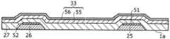
그 다음으로, 액정 표시 패널에서 사용하기 위한 통상의 무정형 규소 박막 트랜지스터 기판의 구조 및 작동 원리에 대하여서는 도 2를 참조하여 상세하게 예시될 것이다. 도 2는 도 1의 "A"의 요부 확대도이다.Next, the structure and operating principle of a conventional amorphous silicon thin film transistor substrate for use in a liquid crystal display panel will be illustrated in detail with reference to FIG. FIG. 2 is an enlarged view illustrating main parts of “A” of FIG. 1.
도 2를 참조하면, 주사선(박막 게이트 배선)(25)은 유리 기판(도시하지 않음)상에 배치된다. 주사선(25)의 일부는 박막 트랜지스터를 제어(온 및 오프 작동)하기 위한 게이트 전극(26)으로서 작동한다. 게이트 절연체(질화규소막)(27)는 게이트 전극(26)을 도포하도록 배치된다. 신호선 (소스/드레인 배선)(34)은 이들 사이에 개재된 게이트 절연체(27)와 주사선(25)이 교차하도록 배치된다. 신호선(34)의 일부는 박막 트랜지스터의 소스 전극(28)으로서 작동한다. 게이트 절연체(27)의 부근에는 무정형 규소 채널막(활성 반도체막)(33), 신호선(소스/드레인 배선)(34) 및 질화규소 층간 유전막(보호막)(30)이 배치된다. 이러한 유형의 액정 표시 패널은 일반적으로 보텀 게이트형(bottom gate type) 패널로서 지칭된다.Referring to Fig. 2, a scanning line (thin film gate wiring) 25 is disposed on a glass substrate (not shown). Part of the
무정형 규소 채널 막(33)은 인(P)으로 도핑된 도핑층(n층) 및 고유층(i층; 비도핑층으로도 지칭됨)을 포함한다. 게이트 절연체(27)에는 화소 영역이 있으며, 여기에는 투명 화소 전극(5)이 배치된다. 투명 화소 전극(5)은 예를 들면 In2O3 및 SnO를 포함하는 ITO 막으로 생성된다. 박막 트랜지스터의 드레인 전극(29)은 후술하는 장벽 금속층(barrier metal layer)을 개재시켜 투명 화소 전극(5)에 접촉 및 전기 접속된다.The amorphous
게이트 전압을 주사선(25)을 통하여 게이트 전극(26)에 인가하는 경우, 박막 트랜지스터(4)는 온 작동된다. 이러한 상태에서, 신호선(34)에 인가되는 구동 전압은 소스 전극(28)으로부터 드레인 전극(29)을 통하여 투명 화소 전극(5)으로 인가된다. 투명 화소 전극(5)이 소정 수준에서 구동 전압으로 인가될 경우, 도 1을 참조하여 전술한 바와 같이 투명 화소 전극(5)과 대향 전극(2)의 사이에는 전위차가 발생한다. 이러한 전위차는 액정층(3)에서의 액정 분자를 배향 또는 정렬시켜 광 변조를 일으키게 된다.When the gate voltage is applied to the
박막 트랜지스터 기판(1)에서, 소스/드레인 전극에 전기 접속된 소스/드레인 배선(34), 투명 화소 전극(5)에 전기 접속된 신호선(화소 전극용 신호선); 게이트 전극(26)에 전기 접속된 주사선(25)은 각각 순수한 합금 또는 알루미늄 합금, 예컨대 Al-Nd(이하, 순수한 알루미늄 및 알루미늄 합금을 "알루미늄 합금"으로 통칭함)의 박막으로 제조된다. 이는 이와 같은 순수한 알루미늄 또는 알루미늄 합금이 저항률이 낮고, 용이하게 가공될 수 있기 때문이다. 내화성 금속, 예컨대 Mo, Cr, Ti 또는 W를 포함하는 장벽 금속층(51, 52, 53 및 54)을 도 2에 도시한 바와 같이 이들 배선의 위 및 아래에 배치한다.A thin
통상의 알루미늄 합금 박막이 장벽 금속층을 개재시켜 다른 구성요소에 접속되어야만 하는 이유는 하기에서 설명될 것이다. 알루미늄 합금 박막은 도 2에 도시한 바와 같이 장벽 금속층(51, 52)을 개재시켜 투명 화소 전극(5)에 접속된다. 이는 알루미늄 합금 박막이 투명 화소 전극에 직접 접속될 경우 이들 부품 사이의 접촉 저항이 높게 되어 표시된 화상의 품질을 손상시키기 때문이다. 투명 화소 전극에 대한 배선을 위한 소재로서 사용되는 알루미늄은 산화되기 쉬우며, 산화알루미늄의 절연층은 알루미늄 합금 박막과 투명 화소 전극 사이의 계면에서 형성된다. 산화알루미늄은 액정 표시 패널의 성막 공정중에 형성되거나 첨가된 산소로부터 유래한다. 투명 화소 전극을 위한 물질로서 인듐 주석 산화물(ITO)은 전기 전도성 금속 산화물이기는 하나, 이는 알루미늄 산화물층이 형성된 경우 전기적 오옴 접촉(ohmic contact)을 형성하지 못한다.The reason why a conventional aluminum alloy thin film must be connected to other components via a barrier metal layer will be described below. The aluminum alloy thin film is connected to the
그러나, 이러한 장벽 금속층의 형성은, 게이트 전극, 소스 전극 및 드레인 전극의 형성을 위한 스퍼터링 시스템 이외에, 금속층의 형성을 위한 추가의 성막 챔버을 필요로 한다. 이러한 추가의 유닛은 제조 단가를 상승시키며 생산성을 저하시킨다.However, the formation of such a barrier metal layer requires an additional deposition chamber for the formation of the metal layer, in addition to the sputtering system for the formation of the gate electrode, the source electrode and the drain electrode. These additional units raise manufacturing costs and lower productivity.
따라서, 장벽 금속층에 대한 필요성을 배제시키고 소스/드레인 전극과 투명 화소 전극 사이의 직접 접촉이 가능한 전극용 소재에 대한 제안이 이루어져 왔었다.Accordingly, there has been a proposal for an electrode material that eliminates the need for a barrier metal layer and enables direct contact between the source / drain electrode and the transparent pixel electrode.
일본 특허 공개 공보 제1999-337976호에는 투명 화소 전극용 소재로서 인듐 산화물 및 약 10 중량%의 아연 산화물을 포함하는 인듐 아연 산화물(IZO)을 사용하는 기법이 개시되어 있다. 그러나, 이러한 기법에 의하면, 가장 널리 사용되고 있는 ITO 막은 IZO 막으로 대체되어야 하지만, 이러한 IZO 막은 재료 원가의 상승을 초래한다.Japanese Patent Laid-Open No. 1999-337976 discloses a technique using indium zinc oxide (IZO) containing indium oxide and about 10% by weight zinc oxide as a material for a transparent pixel electrode. However, according to this technique, the most widely used ITO film should be replaced with an IZO film, but such an IZO film causes an increase in material cost.
일본 특허 공개 공보 제1999-283934호에는 드레인 전극을 플라즈마 처리 또는 이온 주입으로 처리하여 드레인 전극의 표면을 개질시키는 방법이 개시되어 있다. 그러나, 이러한 방법은 표면 처리를 위한 추가의 단계를 필요로 하는데, 이는 생산성의 저하를 초래한다.Japanese Patent Laid-Open No. 1999-283934 discloses a method of modifying the surface of a drain electrode by treating the drain electrode by plasma treatment or ion implantation. However, this method requires an additional step for surface treatment, which leads to a decrease in productivity.
일본 특허 공개 공보 제1999-284195호에는 순수한 알루미늄 또는 알루미늄 합금의 제1층 및, 질소, 산소, 규소 및 탄소와 같은 불순물을 추가로 포함하는 알루미늄 합금 또는 순수한 알루미늄의 제2층으로부터 게이트 전극, 소스 전극 및 드레인 전극을 구성하는 방법이 개시되어 있다. 이러한 방법은 게이트 전극, 소스 전극 및 드레인 전극을 구성하기 위한 박막이 하나의 성막 챔버에서 연속적으로 형성될 수 있는 잇점을 갖는다. 그러나, 이러한 방법은 불순물을 포함하는 제2의 층을 형성하는 추가의 단계를 필요로 한다. 또한, 생성된 소스/드레인 배선은 종종 소스/드레인 배선에 불순물을 투입시키는 단계에서 성막 챔버의 벽면으로부터 박편으로 탈리된다. 이는 불순물을 포함하는 막과, 불순물을 포함하지 않는 막 사이의 열 팽창계수차에 의한 것이다. 이러한 문제점을 해소하기 위하여, 이러한 방법은 잦은 성막 공정의 중지 및 유지 보수를 필요로 하며, 이는 생산성을 심각하게 저하시킨다.Japanese Patent Laid-Open No. 1999-284195 discloses a gate electrode, source from a first layer of pure aluminum or an aluminum alloy and a second layer of aluminum alloy or pure aluminum further comprising impurities such as nitrogen, oxygen, silicon and carbon. A method of constructing an electrode and a drain electrode is disclosed. This method has the advantage that thin films for constructing the gate electrode, the source electrode and the drain electrode can be formed continuously in one deposition chamber. However, this method requires an additional step of forming a second layer containing impurities. In addition, the generated source / drain interconnects are often detached into flakes from the wall surface of the deposition chamber in the step of introducing impurities into the source / drain interconnects. This is due to the thermal expansion coefficient difference between the film containing impurities and the film containing impurities. In order to solve this problem, this method requires frequent stopping and maintenance of the film forming process, which seriously degrades the productivity.
이러한 상황하에서, 본 발명자들은 일본 특허 공개 공보 2004-214606에서 장벽 금속층에 대한 필요성을 배제시키고, 단계의 수를 증가시키지 않으면서 제조 공정을 단순화하고, 투명 화소 전극과 알루미늄 합금막 사이의 직접적이고도 신뢰성 있는 접촉이 가능한 방법을 개시하였다. 일본 특허 공개 공보 2004-214606에 개시된 기법은 합금 원소로서 Au, Ag, Zn, Cu, Ni, Sr, Ge, Sm 및 Bi로 구성된 군에서 선택된 1종 이상을 0.1 내지 6원자% 포함하며, 이러한 합금 원소 중 1종 이상이 알루미늄 합금막과 투명 화소 전극 사이의 계면에서 석출층 또는 농화층이 되도록 하는 알루미늄 합금을 사용하여 목적을 달성하였다.Under these circumstances, the present inventors have eliminated the need for a barrier metal layer in Japanese Patent Laid-Open No. 2004-214606, simplifying the manufacturing process without increasing the number of steps, and directly and reliability between the transparent pixel electrode and the aluminum alloy film. Disclosed is a method in which contact is possible. The technique disclosed in Japanese Patent Laid-Open No. 2004-214606 includes 0.1 to 6 atomic% of one or more selected from the group consisting of Au, Ag, Zn, Cu, Ni, Sr, Ge, Sm, and Bi as alloy elements, and such alloys The object was achieved by using an aluminum alloy such that at least one of the elements is a precipitated layer or a concentrated layer at the interface between the aluminum alloy film and the transparent pixel electrode.
전술한 바와 같이, 일본 특허 공개 공보 2004-214606에 개시된 기법은 알루미늄 합금막과 투명 화소 전극 사이의 직접 접속이 가능하다.As described above, the technique disclosed in Japanese Patent Laid-Open No. 2004-214606 enables direct connection between the aluminum alloy film and the transparent pixel electrode.
그러나, 무정형 규소 박막과, 알루미늄 합금을 포함하는 소스/드레인 배선 사이의 직접 접속이 가능하도록 하는 기법은 개시되어 있지 않다.However, no technique is disclosed to enable direct connection between an amorphous silicon thin film and a source / drain interconnect comprising an aluminum alloy.
전술한 바와 같이, 소스/드레인 배선으로서의 통상의 배선은 각각 알루미늄 합금 박막상에 및 알루미늄 합금 박막의 아래에 배치된 알루미늄 합금 박막 및 장벽 금속층(54 및 53)을 포함한다. 이러한 배선의 대표적인 예로는 두께가 약 50㎚인 몰리브덴(Mo)층 (하부 장벽 금속층), 두께가 약 150㎚인 순수한 알루미늄 또는 Al-Nd 합금 박막, 및 두께가 약 50㎚인 Mo층(상부 장벽 금속층)의 순서로 배치된 것을 포함하는 다층 (3층) 배선이다. 하부 장벽 금속층은 알루미늄 합금 박막과 무정형 규소 박막 사이의 계면에서 규소와 알루미늄의 사이에서의 상호확산을 방지하도록 주로 배치된다. 상부 장벽 금속층은 알루미늄 합금 박막의 표면상에서의 힐록(hillock) (혹 모양 돌기물)이 방지되도록 주로 배치된다. 이러한 메카니즘은 하기에서 상세하게 설명될 것이다.As mentioned above, conventional wiring as source / drain wiring includes aluminum alloy thin films and
그러나, 상부 및 하부 장벽 금속층의 형성은 알루미늄 합금 배선의 형성을 위한 성막 시스템 이외에, 장벽 금속층의 형성을 위한 추가의 성막 시스템을 필요로 한다. 상세하게는, 각각의 장벽 금속 박막의 형성을 위한 추가의 성막 챔버를 포함한 성막 시스템을 사용하여야만 한다. 이러한 시스템의 대표적인 예로는, 이송실에 접속된 복수의 성막 챔버를 비롯한 클러스터 툴 시스템(cluster tool system)이다. 이러한 장벽 금속층의 형성을 위한 추가의 유닛을 포함하는 시스템은 제조 단가를 상승시키며 생산성을 저하시킨다.However, the formation of the upper and lower barrier metal layers requires an additional deposition system for the formation of the barrier metal layer, in addition to the deposition system for the formation of the aluminum alloy wiring. Specifically, a deposition system must be used that includes an additional deposition chamber for the formation of each barrier metal thin film. A representative example of such a system is a cluster tool system including a plurality of deposition chambers connected to a transfer chamber. Systems comprising additional units for the formation of such barrier metal layers increase manufacturing costs and lower productivity.
또한, 습식 에칭에 의한 3층의 다층 배선의 테이퍼링(tapering)은 각각 장벽 금속 및 알루미늄 합금에 대한 상이한 에칭제(에칭액)를 필요로 하며, 에칭제에 적절한 것으로 상이한 에칭조(etching bath)를 추가로 필요로 하여 단가 상승을 초래한다. 예를 들면 순수한 몰리브덴으로부터의 상부 장벽 금속층 및, 몰리브덴 합금으로부터의 하부 장벽 금속층을 구성하여 하나의 에칭제를 사용한 다층 배선의 테이퍼링을 실시하고자 하는 시도가 이루어져 왔었다. 그러나, 이러한 기법은 높은 정확도를 갖는 처리를 실시하지는 못한다.In addition, taping of the three-layer multilayer wiring by wet etching requires different etching agents (etchants) for the barrier metal and the aluminum alloy, respectively, and adds different etching baths as appropriate for the etching agent. It is necessary to raise the unit price. Attempts have been made, for example, to taper multilayer wiring using one etchant by constructing an upper barrier metal layer from pure molybdenum and a lower barrier metal layer from molybdenum alloy. However, this technique does not perform a process with high accuracy.
따라서, 상부 및 하부 장벽 금속층에 대한 필요성을 배제시키고, 소스/드레인 배선을 위하여 무정형 규소 박막 및 알루미늄 합금 박막 사이의 직접적인 접속이 가능한 소스/드레인 전극을 제공하는 것이 강하게 요구되고 있다.Therefore, there is a strong need to eliminate the need for upper and lower barrier metal layers and to provide a source / drain electrode capable of direct connection between an amorphous silicon thin film and an aluminum alloy thin film for source / drain wiring.
표시 디바이스의 제조는 수율 및 생산성을 개선시키기 위하여 저온에서 실시되고 있다. 예를 들면 무정형 규소 박막 트랜지스터에 대한 소스/드레인 전극 소재는 전기 저항률이 약 8μΩ·㎝ 또는 그 이하이고, 약 350℃의 허용 가능한 온도 한계치의 관점에서 높은 열 안정성을 지녀야만 한다. 허용 가능한 온도 한계치는 박막 트랜지스터 기판의 제조 중에 소스/드레인 전극에 적용되는 최고 온도에 의하여 측정된다. 여기서 최고 온도라는 것은 일반적으로 보호막으로서 유전 박막이 전극에 형성되는 온도이다. 성막 기술에서의 근래의 진보는 비교적 저온에서조차도 목적하는 유전 박막의 형성을 실현하였다. 특히, 이러한 진보는 약 200℃에서의 소스/드레인 전극에서의 보호막의 형성을 실현하였다.The manufacture of display devices is carried out at low temperatures in order to improve the yield and productivity. For example, the source / drain electrode material for amorphous silicon thin film transistors should have an electrical resistivity of about 8 μΩ · cm or less and have high thermal stability in view of an acceptable temperature limit of about 350 ° C. Acceptable temperature limits are measured by the highest temperatures applied to the source / drain electrodes during fabrication of the thin film transistor substrate. The highest temperature here is generally the temperature at which the dielectric thin film is formed on the electrode as a protective film. Recent advances in film deposition techniques have resulted in the formation of desired dielectric thin films even at relatively low temperatures. In particular, this advance has realized the formation of a protective film at the source / drain electrodes at about 200 ° C.
그러므로, 소스/드레인 전극 소재는 허용 가능한 온도 한계치가 약 200℃이고, 충분히 낮은 전기 저항률을 지녀야만 한다.Therefore, the source / drain electrode material must have an acceptable temperature limit of about 200 ° C. and have a sufficiently low electrical resistivity.
상기의 설명은 액정 표시 장치를 대표적인 예로 들어 설명하였으나, 종래 기술에서의 문제점은 공통적으로 액정 표시 장치뿐만 아니라 기타의 디바이스에서도 사용되는 무정형 규소 박막 트랜지스터 기판에 존재한다.While the above description has been given by taking a liquid crystal display as a representative example, problems in the prior art are commonly present in amorphous silicon thin film transistor substrates that are used in not only liquid crystal displays but also other devices.
본 발명은 이러한 상황하에서 달성된 것으로서, 본 발명의 목적은 하부 장벽 금속층의 필요성을 배제시키고, 단계의 수를 증가시키지 않으면서 제조 공정을 단순화하였으며 알루미늄 합금막과 무정형 규소 채널막 사이의 직접적이고도 신뢰성 있는 접속이 가능하며, 알루미늄 합금막을 약 100℃ 이상 약 300℃ 이하의 저온에서의 공정으로 처리할 경우조차도 낮은 전기 저항률을 보장하는 소스/드레인 전극을 제공하고자 하는 것이다. 상세하게는, 본 발명의 목적은 저온에서의 공정에 적합하며, 알루미늄 합금막을, 예를 들면 약 200℃와 같은 저온에서 약 20 분간 열 처리로 처리할 경우조차 알루미늄 합금막의 전기 저항률이 8μΩ·㎝ 이하가 되는 것을 보장하는 소스/드레인 전극을 제공하고자 하는 것이다.The present invention has been accomplished under such circumstances, and the object of the present invention is to eliminate the need for a lower barrier metal layer, simplify the manufacturing process without increasing the number of steps, and provide a direct and reliable connection between the aluminum alloy film and the amorphous silicon channel film. It is possible to provide a source / drain electrode which is capable of a reliable connection and guarantees a low electrical resistivity even when the aluminum alloy film is treated in a process at a low temperature of about 100 ° C. or more and about 300 ° C. or less. Specifically, the object of the present invention is suitable for the process at low temperature, and even if the aluminum alloy film is subjected to heat treatment for about 20 minutes at a low temperature such as, for example, about 200 ° C., the electrical resistivity of the aluminum alloy film is 8 μΩ · cm It is intended to provide a source / drain electrode that ensures that:
본 발명의 또다른 목적은 하부 장벽 금속층뿐 아니라 상부 장벽 금속층의 필요성을 배제하여 무정형 규소 채널막뿐 아니라 투명 화소 전극에 알루미늄 합금막을 직접 그리고 신뢰성 있게 접속시킬 수 있는 기법을 제공하고자 하는 것이다.It is another object of the present invention to provide a technique capable of directly and reliably connecting an aluminum alloy film to a transparent pixel electrode as well as an amorphous silicon channel film by eliminating the need for an upper barrier metal layer as well as a lower barrier metal layer.
상세하게는, 본 발명은 기판, 박막 트랜지스터 반도체층, 소스/드레인 전극 및 투명 화소 전극을 포함하는 박막 트랜지스터 기판에 사용하기 위한 소스/드레인 전극을 제공하되, 상기 소스/드레인 전극은 합금 원소로서 0.1 내지 6원자%의 니켈을 포함하는 알루미늄 합금 박막을 포함하며, 여기서 소스/드레인 전극은 알루미늄 합금 박막이 박막 트랜지스터 반도체층에 직접 접속되도록 구성된다.Specifically, the present invention provides a source / drain electrode for use in a thin film transistor substrate including a substrate, a thin film transistor semiconductor layer, a source / drain electrode, and a transparent pixel electrode, wherein the source / drain electrode is 0.1 as an alloying element. An aluminum alloy thin film comprising nickel of 6 to 6 atomic percent, wherein the source / drain electrodes are configured such that the aluminum alloy thin film is directly connected to the thin film transistor semiconductor layer.
알루미늄 합금은 합금 원소로서 Ti, V, Zr, Nb, Mo, Hf, Ta 및 W로 구성된 군에서 선택된 1종 이상의 원소를 0.1 내지 1.0원자%로 추가로 포함하는 것이 바람직하다.The aluminum alloy preferably further contains 0.1 to 1.0 atomic percent of one or more elements selected from the group consisting of Ti, V, Zr, Nb, Mo, Hf, Ta and W as alloy elements.
대안으로 또는 이외에, 알루미늄 합금은 합금 원소로서 Mg, Cr, Mn, Ru, Rh, Pd, Ir, Pt, La, Ce, Pr, Gd, Tb, Dy, Nd, Y, Co 및 Fe로 구성된 군에서 선택된 1 종 이상의 원소를 0.1 내지 2.0원자%로 추가로 포함할 수 있다.Alternatively or in addition, aluminum alloys are alloy elements in the group consisting of Mg, Cr, Mn, Ru, Rh, Pd, Ir, Pt, La, Ce, Pr, Gd, Tb, Dy, Nd, Y, Co and Fe It may further comprise 0.1 to 2.0 atomic% of at least one selected element.
바람직한 실시양태에서, 니켈 함유 화합물은 알루미늄 합금 박막과 박막 트랜지스터 반도체층 사이의 계면에 포함된다.In a preferred embodiment, the nickel containing compound is included at the interface between the aluminum alloy thin film and the thin film transistor semiconductor layer.
니켈 함유 화합물은 알루미늄 합금에 함유된 니켈과 알루미늄의 금속간 화합물; 알루미늄 합금에 포함된 니켈과 박막 트랜지스터 반도체층에 포함된 규소와의 규화물 또는 규소 화합물; 및 알루미늄 합금중의 알루미늄 및 니켈과 박막 트랜지스터 반도체층중의 규소와의 금속간 화합물로 구성된 군에서 선택된 1종 이상의 화합물인 것이 바람직하다.The nickel-containing compound may be an intermetallic compound of nickel and aluminum contained in an aluminum alloy; A silicide or silicon compound of nickel included in an aluminum alloy and silicon included in the thin film transistor semiconductor layer; And at least one compound selected from the group consisting of intermetallic compounds of aluminum and nickel in the aluminum alloy and silicon in the thin film transistor semiconductor layer.
또다른 바람직한 실시양태에서, 알루미늄 합금 박막과 박막 반도체층 사이의 계면에 니켈 농화층을 포함하며, 여기서 상기 니켈 농화층은 평균 니켈 농도가 알루미늄 합금의 평균 니켈 농도의 2 배 이상이다.In another preferred embodiment, a nickel thickening layer is included at the interface between the aluminum alloy thin film and the thin film semiconductor layer, wherein the nickel thickening layer has an average nickel concentration of at least twice the average nickel concentration of the aluminum alloy.
알루미늄 합금 박막은 전기 저항률이 8μΩ·㎝ 이하인 것이 바람직하다.The aluminum alloy thin film preferably has an electrical resistivity of 8 µPa · cm or less.
알루미늄 합금 박막은 투명 화소 전극에 추가로 직접 접속되도록 배치되는 것이 바람직하다.The aluminum alloy thin film is preferably arranged to be further directly connected to the transparent pixel electrode.
또다른 바람직한 실시양태에서, 알루미늄 합금 박막과 투명 화소 전극 사이의 계면에 AlOx를 포함하며, 여기서 x는 산소의 원자비이며, 0<x≤0.8의 조건을 충족한다.In another preferred embodiment, AlOx is included at the interface between the aluminum alloy thin film and the transparent pixel electrode, where x is the atomic ratio of oxygen and meets the condition of 0 <x ≦ 0.8.
또다른 바람직한 실시양태에서, 알루미늄 합금 박막과 투명 화소 전극 사이의 계면에 니켈 농화층을 포함하며, 여기서 상기 니켈 농화층의 평균 니켈 농도는 알루미늄 합금의 평균 니켈 농도의 2 배 이상이다.In another preferred embodiment, a nickel thickening layer is included at the interface between the aluminum alloy thin film and the transparent pixel electrode, wherein the average nickel concentration of the nickel thickening layer is at least twice the average nickel concentration of the aluminum alloy.
투명 화소 전극은 인듐-주석-산화물(ITO) 또는 인듐 아연 산화물(IZO)을 포함하는 것이 바람직하다.The transparent pixel electrode preferably includes indium tin oxide (ITO) or indium zinc oxide (IZO).
본 발명은 추가로 이들 소스/드레인 전극 중 임의의 것을 포함하는 박막 트랜지스터 기판을 추가로 제공한다.The present invention further provides a thin film transistor substrate comprising any of these source / drain electrodes.
본 발명은 박막 트랜지스터 기판을 포함하는 표시 디바이스를 추가로 제공한다.The present invention further provides a display device comprising a thin film transistor substrate.
추가로, 및 유리하게는, 본 발명은In addition, and advantageously, the present invention
(a) 박막 트랜지스터 반도체층을 갖는 기판을 생성하는 단계,(a) generating a substrate having a thin film transistor semiconductor layer,
(b) 박막 트랜지스터 반도체층상에 알루미늄 합금 박막을 형성하는 단계,(b) forming an aluminum alloy thin film on the thin film transistor semiconductor layer,
(c) 알루미늄 합금 박막상에 질화규소막을 형성하는 단계를 포함하며,(c) forming a silicon nitride film on the aluminum alloy thin film,
여기서 단계 (c)는 100℃ 이상 300℃ 이하의 온도에서 가열을 수행하는 단계를 포함하는, 박막 트랜지스터 기판의 제조 방법을 제공한다. 단계 (b)는 스퍼터링 공정을 포함하는 것이 바람직하다.Wherein step (c) provides a method of manufacturing a thin film transistor substrate, comprising performing heating at a temperature of at least 100 ° C and at most 300 ° C. Step (b) preferably comprises a sputtering process.
본 발명에 따른 소스/드레인 전극은 전술한 구조를 가지며, 이에 의하여 알루미늄 합금 박막 및 박막 트랜지스터 반도체층 사이의 직접 접속이 가능하게 된다. 바람직한 실시양태에서, 알루미늄 합금 박막과 투명 화소 전극 사이의 직접 접속이 가능하게 된다. 그리하여, 생산성이 우수하면서도 저렴한 고 성능 표시 디바이스를 제공할 수 있다.The source / drain electrodes according to the present invention have the above-described structure, thereby enabling direct connection between the aluminum alloy thin film and the thin film transistor semiconductor layer. In a preferred embodiment, a direct connection between the aluminum alloy thin film and the transparent pixel electrode is enabled. Thus, it is possible to provide a high performance display device which is excellent in productivity and inexpensive.
본 발명에 따른 소스/드레인 전극은 약 200℃의 비교적 낮은 온도에서 열처리를 실시하는 경우에서도 충분히 낮은 전기 저항을 제공한다. 본 명세서에서 사용한 용어 "열 처리 온도"라는 것은 TFT 어레이 기판의 제조 공정중에서의 최고 온도를 지칭한다. 이는, 예를 들면 일반적으로 표시 디바이스를 위한 박막 트랜지스터 기판의 제조 방법인 보호막의 열경화를 위한 가열 퍼니스의 온도 또는 CVD 성막에서 기판을 가열하는 온도에 해당한다.The source / drain electrodes according to the present invention provide sufficiently low electrical resistance even when the heat treatment is performed at a relatively low temperature of about 200 ° C. The term "heat treatment temperature" as used herein refers to the highest temperature in the manufacturing process of a TFT array substrate. This corresponds to, for example, the temperature of a heating furnace for thermal curing of a protective film, which is generally a method of manufacturing a thin film transistor substrate for a display device, or the temperature of heating a substrate in CVD film formation.
추가로, 본 발명의 목적, 특징 및 잇점은 본 명세서에 첨부한 도면을 참조하여 하기의 바람직한 실시양태의 설명으로부터 명백할 것이다.In addition, the objects, features and advantages of the present invention will become apparent from the following description of the preferred embodiments with reference to the accompanying drawings.
본 발명자들은 소스/드레인 전극을 위한 알루미늄 합금 박막 및 박막 트랜지스터 반도체층 사이의 직접적이고도 신뢰성 있는 접속을 위한 신규한 기술을 제공하기 위하여 예의 검토하였다. 그 결과, 본 발명자들은 알루미늄 합금 박막과 박막 트랜지스터 반도체층 사이의 계면에서 알루미늄과 규소간의 상호확산이 방지될 수 있으며, 소스/드레인 전극을 위한 알루미늄 합금으로서 0.1 내지 6원자%의 니켈을 함유하는 알루미늄 합금을 사용하여 이러한 목적이 달성될 수 있다는 것을 발견하였다. 본 발명은 이러한 발견에 기초하여 이루어진 것이다. 본 발명은 하부 장벽 금속층뿐 아니라 상부 장벽 금속층의 필요성을 배제하여 박막 트랜지스터 반도체층뿐 아니라 투명 화소 전극으로의 Al-Ni 합금 박막의 직접 접속이 가능하게 된다.The inventors have intensively studied to provide a novel technique for direct and reliable connection between aluminum alloy thin films for source / drain electrodes and thin film transistor semiconductor layers. As a result, the inventors can prevent the interdiffusion between aluminum and silicon at the interface between the aluminum alloy thin film and the thin film transistor semiconductor layer, and contain aluminum containing 0.1 to 6 atomic percent nickel as the aluminum alloy for the source / drain electrodes. It has been found that this object can be achieved using alloys. The present invention has been made based on this finding. The present invention eliminates the need for the upper barrier metal layer as well as the lower barrier metal layer, thereby enabling direct connection of the Al—Ni alloy thin film to the transparent pixel electrode as well as the thin film transistor semiconductor layer.
본 명세서에서 사용한 용어 "소스/드레인 전극"은 소스/드레인 전극 자체 및 소스/드레인 배선 모두를 포함하는 것을 의미한다. 상세하게는, 본 발명에 따른 소스/드레인 전극 각각은 소스/드레인 배선에 집적된 소스/드레인 전극을 포함하며, 여기서 소스/드레인 배선은 소스/드레인 영역과 접촉된다.As used herein, the term "source / drain electrode" is meant to include both the source / drain electrode itself and the source / drain wiring. Specifically, each of the source / drain electrodes according to the present invention includes a source / drain electrode integrated in the source / drain wiring, wherein the source / drain wiring is in contact with the source / drain region.
본 발명의 구조에 대하여 상세히 설명하기 이전에, 본 발명자들이 본 발명을 도출하게 된 배경은 일본 특허 공개 공보 제2004-214606호에 개시된 기술을 참조하여 설명할 것이다.Before describing the structure of the present invention in detail, the background on which the present inventors derive the present invention will be described with reference to the technique disclosed in Japanese Patent Laid-Open No. 2004-214606.
상세하게는, 본 발명자들은 액정 표시 디바이스에 사용하기 위한 배선 소재의 생산성 및 물성을 개선시키고자 예의 연구한 바 있다.In detail, the present inventors earnestly studied to improve the productivity and physical properties of wiring materials for use in liquid crystal display devices.
우선, 본 발명자들은 투명 화소 전극을 위한 배선에 관심을 집중하였으며, 예를 들면 투명 화소 전극에 직접 접속될 수 있는 알루미늄 합금으로서, 합금 원소로서 Au 또는 Ag와 같은 귀금속을 미량 포함하는 합금 박막을 개발하였다(일본 특허 공개 공보 제2004-214606호). 일본 특허 공개 공보 제2004-214606호에 개시된 알루미늄 합금을 사용함으로써, 통상의 등가물과는 대조적으로, 계면에서의 산화알루미늄의 절연층의 형성을 방지할 수 있었다. 이는 전기 절연 석출물이 알루미늄 합금 박막과 투명 화소 전극 사이의 계면에서 형성되며, 대부분의 접촉 전류는 석출물을 통과하기 때문이었다.First, the inventors have focused their attention on the wiring for the transparent pixel electrode. For example, as an aluminum alloy that can be directly connected to the transparent pixel electrode, an alloy thin film containing a trace amount of a noble metal such as Au or Ag as an alloying element is developed. (Japanese Patent Laid-Open No. 2004-214606). By using the aluminum alloy disclosed in Japanese Patent Laid-Open No. 2004-214606, it was possible to prevent the formation of an insulating layer of aluminum oxide at the interface as opposed to the usual equivalents. This is because the electrically insulating precipitate is formed at the interface between the aluminum alloy thin film and the transparent pixel electrode, and most of the contact current passes through the precipitate.
그 다음, 본 발명자들은 소스/드레인 전극에 관심을 집중하였으며, 통상의 등가물과는 대조적으로, 통상적으로 몰리브덴의 장벽 금속층의 개재 없이 박막 트랜지스터 반도체층에 직접 접속이 가능한 알루미늄 합금을 제공하는 연구를 하였었다. 이러한 목적을 달성하기 위하여, 일본 특허 공개 공보 제2004-214606호에 개시된 기술과는 상이하게, 소스/드레인 배선을 위한 알루미늄 합금 박막과 박막 트랜지스터 반도체층 사이의 계면에서 규소와 알루미늄 사이의 상호확산을 방지할 수 있다. 이러한 관점에서, 본 발명자들은 무수한 실험을 실시하였으며, 그리하여 알루미늄 합금에 혼입될 수 있는 각종의 원소중에서도 니켈(Ni)은 규소와 알루미늄 사이의 상호확산을 효과적으로 방지할 수 있다는 사실을 발견하였다. 본 발명은 이러한 발견에 기초하여 달성되었다. 이와 관련하여, 상호확산의 메카니즘은 하기에서 상세하게 설명할 것이다.Next, the inventors focused their attention on the source / drain electrodes and, in contrast to the conventional equivalents, studied to provide an aluminum alloy that can be directly connected to the thin film transistor semiconductor layer, without intervening a barrier metal layer of molybdenum. . In order to achieve this purpose, unlike the technique disclosed in Japanese Patent Laid-Open No. 2004-214606, the interdiffusion between silicon and aluminum at the interface between the aluminum alloy thin film and the thin film transistor semiconductor layer for source / drain wiring is performed. You can prevent it. In view of this, the present inventors have conducted a myriad of experiments, and thus found that nickel (Ni) can effectively prevent the interdiffusion between silicon and aluminum, among various elements that can be incorporated into aluminum alloys. The present invention has been accomplished based on this finding. In this regard, the mechanism of interdiffusion will be described in detail below.
이하에서는, 알루미늄 합금 박막과 박막 트랜지스터 반도체층 사이의 계면(이하, 이를 "계면"으로 지칭함)에서 규소와 알루미늄 사이의 상호확산을 설명하고자 한다.Hereinafter, the interdiffusion between silicon and aluminum at the interface between the aluminum alloy thin film and the thin film transistor semiconductor layer (hereinafter referred to as "interface") will be described.
통상적으로 몰리브덴으로 생성된 하부 장벽 금속층은 통상적으로는 박막 트랜지스터 반도체층에 접속시키기 위하여 알루미늄 합금 박막의 아래에 배치된다. 이는 주로 계면에서의 규소가 박막 트랜지스터의 형성중에 열 처리의 결과로서 알루미늄 합금 박막으로 확산되며, 이는 알루미늄 합금 박막의 전기 저항을 증가시키기 때문이다. 상세하게는, 알루미늄 합금 박막으로 확산된 규소는 석출된 규소 입자(grain)를 형성하며, 이들은 고체상으로 성장하여 절연성 규소 섬을 형성함으로써 소스/드레인 전극의 전기 저항을 증가시키게 된다.The lower barrier metal layer, typically made of molybdenum, is typically disposed underneath the aluminum alloy thin film to connect to the thin film transistor semiconductor layer. This is mainly because silicon at the interface diffuses into the aluminum alloy thin film as a result of heat treatment during formation of the thin film transistor, which increases the electrical resistance of the aluminum alloy thin film. Specifically, silicon diffused into an aluminum alloy thin film forms precipitated silicon grains, which grow in the solid phase to form insulating silicon islands, thereby increasing the electrical resistance of the source / drain electrodes.
또한, 알루미늄은 규소의 확산과 동시에 계면에서 박막 트랜지스터 반도체층으로 확산된다. 박막 트랜지스터 반도체층으로 확산된 알루미늄은 반도체층으로 도핑된 인의 캐리어를 보충하는 역할을 하는데, 이는 계면에서의 접촉 저항을 증가 시킨다.In addition, aluminum diffuses from the interface to the thin film transistor semiconductor layer simultaneously with the diffusion of silicon. Aluminum diffused into the thin film transistor semiconductor layer serves to supplement the carrier of phosphorus doped into the semiconductor layer, which increases the contact resistance at the interface.
박막 트랜지스터 반도체층으로 확산된 알루미늄은 규소 결핍층(하전이 0인 부위)으로 추가로 확산되어 결함 레벨(defect level)을 형성하는데, 이는 반도체층을 통과하는 비정상적인 전류를 야기하게 된다. 이는 박막 트랜지스터가 오프 작동(오프-상태의 전류)될 경우 통과하는 전류의 누출을 증가시키게 되며, 스위칭 작동은 달성될 수 없다. 또한, 박막 트랜지스터는 오프 작동시 추가로 큰 전원을 소비하게 된다.Aluminum diffused into the thin film transistor semiconductor layer is further diffused into the silicon deficient layer (zero charge region) to form a defect level, which causes abnormal current passing through the semiconductor layer. This increases the leakage of current passing when the thin film transistor is turned off (off-state current), and switching operation cannot be achieved. In addition, the thin film transistors consume an additional large power source in the off operation.
결론적으로, 본 발명에서 알루미늄에 첨가하고자 하는 합금 원소의 성질의 요건은 전술한 일본 특허 공개 공보 제2004-214606호에 언급된 기술의 요건과는 상이하다. 상세하게는, 일본 특허 공개 공보 제2004-214606호에 개시된 기술은 투명 화소 전극에 직접 접속시키고자 하는 배선 소재로서 알루미늄 합금을 사용하고, 알루미늄 합금 박막과 투명 화소 전극 사이의 계면에서 알루미늄의 산화를 방지하는 관점에서 알루미늄 합금에 첨가하고자 하는 원소를 상술하였다. 반대로, 본 발명은 박막 트랜지스터 반도체층에 직접 접속시키고자 하는 소스/드레인 배선 소재로서 알루미늄 합금을 사용하며, 알루미늄 합금 박막과 반도체층 사이의 계면에서 규소의 확산을 방지하는 점에서 알루미늄 합금에 첨가하고자 하는 원소를 구체화하였다. 이러한 2 가지의 기법은 배선 소재의 물성 요건에 있어서 상이하다.In conclusion, the requirements of the properties of the alloying elements to be added to aluminum in the present invention are different from the requirements of the technique mentioned in Japanese Patent Laid-Open No. 2004-214606. Specifically, the technique disclosed in Japanese Patent Laid-Open No. 2004-214606 uses aluminum alloy as a wiring material to be directly connected to a transparent pixel electrode, and oxidizes aluminum at the interface between the aluminum alloy thin film and the transparent pixel electrode. The element to add to an aluminum alloy from the viewpoint of prevention was mentioned above. On the contrary, the present invention uses aluminum alloy as a source / drain wiring material to be directly connected to the thin film transistor semiconductor layer, and is intended to be added to the aluminum alloy in terms of preventing diffusion of silicon at the interface between the aluminum alloy thin film and the semiconductor layer. The element to make was specified. These two techniques differ in the physical property requirements of the wiring material.
그 다음, 본 발명에 사용하기 위한 Al-Ni 합금을 예시하고자 한다.Next, an Al-Ni alloy for use in the present invention is illustrated.
전술한 바와 같이 0.1 내지 6원자%의 니켈을 포함하는 알루미늄 합금을 본 발명에서 소스/드레인 전극으로서 사용하였다. 이를 충족하기 위하여서는 니켈 함유 석출물 또는 니켈 농화층이 비교적 낮은 온도에서의 열 처리의 결과로서 Al-Ni 합금과 박막 트랜지스터 반도체층 사이의 접촉 계면에서 형성될 수 있다. 상기의 석출물 및 니켈 농화층은 계면에서 규소와 알루미늄의 확산을 방지하는 역할을 하여 오프-상태의 전류를 감소시키게 된다. (하기의 실험예를 참조한다)As described above, aluminum alloys containing 0.1 to 6 atomic percent nickel were used as source / drain electrodes in the present invention. To satisfy this, a nickel-containing precipitate or a nickel thickened layer can be formed at the contact interface between the Al-Ni alloy and the thin film transistor semiconductor layer as a result of heat treatment at a relatively low temperature. The precipitate and the nickel thickening layer serve to prevent the diffusion of silicon and aluminum at the interface to reduce the off-state current. (See the experimental example below.)
본 명세서에서 사용한 "니켈 함유 석출물"이라는 것은 알루미늄 합금에 함유된 니켈과 알루미늄의 금속간 화합물; 알루미늄 합금에 포함된 니켈과 박막 트랜지스터 반도체층중의 규소와의 규화물 또는 규소 화합물; 및 알루미늄 합금중의 알루미늄 및 니켈과 박막 트랜지스터 반도체층중의 규소와의 금속간 화합물로 구성된 군에서 선택된 1종 이상의 화합물을 의미한다.As used herein, "nickel-containing precipitate" refers to an intermetallic compound of nickel and aluminum contained in an aluminum alloy; A silicide or silicon compound of nickel contained in an aluminum alloy with silicon in the thin film transistor semiconductor layer; And at least one compound selected from the group consisting of intermetallic compounds of aluminum and nickel in the aluminum alloy and silicon in the thin film transistor semiconductor layer.
"니켈 농화층"이라는 것은 Al-Ni 합금 박막과 박막 트랜지스터 반도체층 사이의 계면에 위치하며 평균 니켈 농도가 Al-Ni 합금의 평균 니켈 농도보다 2 배 이상(바람직하게는 2.5 배 이상) 높은 층을 의미한다. 니켈 농화층은 두께가 바람직하게는 0.5㎚ 이상 10㎚ 이하, 더욱 바람직하게는 1.0㎚ 이상 5㎚ 이하이다.The nickel enriched layer is located at the interface between the Al-Ni alloy thin film and the thin film transistor semiconductor layer, and the average nickel concentration is two times higher than the average nickel concentration of the Al-Ni alloy (preferably 2.5 times higher). it means. The nickel thickened layer is preferably 0.5 nm or more and 10 nm or less, more preferably 1.0 nm or more and 5 nm or less.
니켈 함량이 0.1원자% 미만인 경우, Al-Ni 합금과 무정형 규소 박막(반도체층) 사이의 계면에서 규소 및 알루미늄의 확산은 하기의 실험예에서 예시한 바와같이 효과적으로 방지될 수 없다. 반대로, 니켈 함량이 6원자%를 초과할 경우, Al-Ni 합금 박막은 지나치게 높은 전기 저항을 지닐 수 있다. 그래서, 화소의 반응 속도가 감소하게 되며, 전력 소비는 증가하게 되고, 그 결과 표시는 실제의 사용에 적절하지 않은 손상된 품질을 갖게 된다. 본 발명의 니켈 함량의 범위는 이러한 잇점 및 단점을 고려하여 설정한 것이다. 니켈 함량은 0.5원자% 이상 5원자% 이하인 것이 바람직하다.When the nickel content is less than 0.1 atomic%, diffusion of silicon and aluminum at the interface between the Al-Ni alloy and the amorphous silicon thin film (semiconductor layer) cannot be effectively prevented as illustrated in the following experimental example. In contrast, when the nickel content exceeds 6 atomic%, the Al-Ni alloy thin film may have an excessively high electrical resistance. Thus, the response speed of the pixel is reduced, the power consumption is increased, and as a result, the display has a damaged quality which is not suitable for actual use. The nickel content of the present invention is set in consideration of these advantages and disadvantages. It is preferable that nickel content is 0.5 atomic% or more and 5 atomic% or less.
본 발명에 사용하기 위한 Al-Ni 합금은 합금 원소로서 Ti, V, Zr, Nb, Mo, Hf, Ta 및 W로 구성된 군(이하, 이러한 군을 "α군"으로 지칭함)에서 선택된 1종 이상의 원소 0.1 내지 1.0원자%를 추가로 포함하는 것이 바람직하다. α군에 속하는 1종 이상의 원소를 포함하는 Al-Ni 합금(이하, "Al-Ni-α 합금"으로 지칭함)은 규소와 알루미늄 사이의 상호확산을 추가로 효과적으로 방지하며, 알루미늄 합금 박막의 표면상의 힐록(혹 모양 돌기물)의 형성을 효과적으로 방지한다. α군에 속하는 1종 이상의 원소의 함량이 0.1원자% 미만인 경우, 이들 원소의 활성은 효과적으로 나타나지 않을 수 있다. 반대로, 이러한 함량이 1.0원자%를 초과할 경우, 활성은 증가될 수 있으나, Al-Ni-α 합금 박막은 필름 소재에 대한 전기 저항률이 증가될 수 있다. 이러한 점을 고려하여, α군에 속하는 1종 이상의 원소의 함량은 0.2원자% 이상 0.8원자% 이하인 것이 더욱 바람직하다. 이들 원소 각각은 단독으로 사용될 수 있거나 또는 조합하여 사용될 수 있다. 이들이 조합하여 사용될 경우, 원소의 총 함량은 상기의 범위 이내에 포함되어야만 한다.Al-Ni alloy for use in the present invention is one or more selected from the group consisting of Ti, V, Zr, Nb, Mo, Hf, Ta and W as the alloying elements (hereinafter referred to as "α group") It is preferable to further contain 0.1 to 1.0 atomic percent of the elements. Al-Ni alloys (hereinafter referred to as "Al-Ni-α alloys") containing at least one element belonging to the α group further effectively prevent the interdiffusion between silicon and aluminum, and on the surface of the aluminum alloy thin film It effectively prevents the formation of hillocks. When the content of one or more elements belonging to the α group is less than 0.1 atomic%, the activity of these elements may not be effectively exhibited. On the contrary, when the content exceeds 1.0 atomic%, the activity may be increased, but the Al-Ni-α alloy thin film may increase the electrical resistivity of the film material. In view of this point, the content of at least one element belonging to the α group is more preferably 0.2 atomic% or more and 0.8 atomic% or less. Each of these elements may be used alone or in combination. When used in combination, the total content of elements must fall within the above range.
대안으로 또는 추가로, 본 발명에 사용하기 위한 Al-Ni 합금은 Mg, Cr, Mn, Ru, Rh, Pd, Ir, Pt, La, Gd, Tb, Dy, Nd, Y, Co, Ce, Pr 및 Fe(이하, "β군"으로 지칭함)로 구성된 군에서 선택된 1종 이상의 원소를 0.1 내지 2.0원자%로 추가로 포함하는 것이 바람직하다. β군에 속하는 1종 이상의 원소를 포함하는 Al-Ni 합금(이하, "Al-Ni-β 합금"으로 지칭함)은 규소와 알루미늄 사이의 상호확산을 추가로 효과적으로 방지하며, 알루미늄 합금 박막의 표면상에서의 힐록(혹 모양 돌기물)의 형성을 효과적으로 방지한다. β군에 속하는 1종 이상의 원소의 함량이 0.1원자% 미만인 경우, 활성은 효과적으로 나타날 수 없다. 그러나, 이러한 함량이 2.0원자%를 초과하는 경우, 활성은 증가될 수 있으나, Al-Ni-β 합금 박막의 저항률이 증가될 수 있다. 이러한 점을 고려하여, β군에 속하는 1종 이상의 원소의 함량은 0.3원자% 이상 1.8원자% 이하인 것이 더욱 바람직하다. 이들 원소 각각은 단독으로 사용될 수 있거나 또는 조합하여 사용될 수 있다. 이들이 조합하여 사용될 경우, 원소의 총 함량은 상기의 범위 이내에 포함되어야만 한다.Alternatively or additionally, Al—Ni alloys for use in the present invention may comprise Mg, Cr, Mn, Ru, Rh, Pd, Ir, Pt, La, Gd, Tb, Dy, Nd, Y, Co, Ce, Pr And Fe (hereinafter referred to as "β group"), preferably further comprises 0.1 to 2.0 atomic percent of at least one element selected from the group consisting of. Al-Ni alloys (hereinafter referred to as "Al-Ni-β alloys") containing one or more elements belonging to the β group further effectively prevent the interdiffusion between silicon and aluminum, and on the surface of the aluminum alloy thin film It effectively prevents the formation of heellocks. When the content of one or more elements belonging to the β group is less than 0.1 atomic%, activity cannot be effectively exhibited. However, when this content exceeds 2.0 atomic%, the activity may be increased, but the resistivity of the Al-Ni-β alloy thin film may be increased. In view of this point, the content of at least one element belonging to the beta group is more preferably 0.3 atomic% or more and 1.8 atomic% or less. Each of these elements may be used alone or in combination. When used in combination, the total content of elements must fall within the above range.
본 발명에서 사용하기 위한 Al-Ni 합금은 α군에 속하는 1종 이상의 원소 및 β군에 속하는 1종 이상의 원소 모두를 포함하는 Al-Ni-α-β 합금이 될 수 있다.The Al-Ni alloy for use in the present invention may be an Al-Ni-α-β alloy including both one or more elements belonging to the α group and one or more elements belonging to the β group.
힐록의 형성 메카니즘을 하기에서 설명하고자 한다.The formation mechanism of Hillock will be described below.
힐록은 아마도 하기와 같은 방식으로 형성될 것이다. 일반적으로 약 300℃∼약 400℃의 열 처리는 박막 트랜지스터 기판의 제조 공정에서 순수한 알루미늄 또는 알루미늄 합금 박막의 형성후 질화규소막(보호막)을 형성할 때 실시된다. 상세하게, 알루미늄 합금 박막으로 도포된 기판은 통상적으로 화학 증착(CVD)으로 처리되어 질화규소막(보호막)이 형성된다. 힐록은 아마도 이러한 열 처리중에 알루미늄 합금 박막과 유리 기판 사이의 열 팽창 계수차에 의하여 야기될 것이다.Hillock may be formed in the following way. In general, heat treatment at about 300 ° C. to about 400 ° C. is performed when a silicon nitride film (protective film) is formed after the formation of a pure aluminum or aluminum alloy thin film in the manufacturing process of the thin film transistor substrate. In detail, the substrate coated with the aluminum alloy thin film is usually treated by chemical vapor deposition (CVD) to form a silicon nitride film (protective film). Hillock is probably caused by the thermal expansion coefficient difference between the aluminum alloy thin film and the glass substrate during this heat treatment.
이러한 α군 및 β군에 속하는 원소는 열 안정성을 증가시키는 점, 및 생성된 Al-Ni-α 합금 박막 또는 Al-Ni-β 합금 박막의 전기 저항률을 감소시키는 점에서 선택된다. α군 및 β군은 열 안정성에 기여하는 메카니즘에서 서로 약간 상이하다. 이는 도 12를 참조하여 하기에서 상세하게 설명될 것이다.The elements belonging to the α group and the β group are selected from the point of increasing thermal stability and decreasing the electrical resistivity of the resulting Al-Ni-α alloy thin film or Al-Ni-β alloy thin film. Groups α and β differ slightly from each other in the mechanisms that contribute to thermal stability. This will be described in detail below with reference to FIG. 12.
도 12는 알루미늄 박막의 응력이 온도에 따라 어떻게 변경하는지를 도시하는 도표이다. 도 12에서의 기호 "A", "B" 및 "C"는 각각 순수한 알루미늄, β군에 속하는 원소를 포함하는 Al-β 합금, 및 α군에 속하는 원소를 포함하는 Al-α 합금의 데이타를 나타낸다.12 is a chart showing how the stress of the aluminum thin film changes with temperature. The symbols "A", "B", and "C" in FIG. 12 indicate data of pure aluminum, an Al-β alloy containing an element belonging to the β group, and an Al-α alloy containing an element belonging to the α group, respectively. Indicates.
도 12에는 β군 합금에 속하는 원소를 포함하는 Al-β 합금막인 "B"가 온도 상승에 따라 압축 응력이 증가하는 것으로 나타나 있다. 입자 성장은 온도 상승의 초기 단계에서는 억제되나, 이는 비교적 낮은 온도에서 개시되며, 좁은 범위의 온도에서 응력은 급격하게 완화된다. 이는 아마도 합금에 함유된 용해 원소가 금속간 화합물로서 석출되며, 이는 알루미늄의 입자 성장을 촉진하여 전기 저항률을 감소시키기 때문이다. 상세하게는, 전기 저항률은 비교적 낮은 가열 온도에서 충분히 감소시키기 때문이다. 그러나, 응력이 충분히 완화되는 상태에서 박막이 추가로 가열될 경우, 압축 응력이 박막에 발생하게 되며, 이는 결정 입자를 돌출시켜 예를 들면 힐록을 생성하게 된다. 합금은 아마도 응력이 완화되는 온도 부근에서 허용 가능한 온도 한계치를 갖는다.12, it is shown that "B", which is an Al-β alloy film containing an element belonging to the β group alloy, increases in compressive stress with increasing temperature. Particle growth is suppressed in the early stages of temperature rise, but it starts at a relatively low temperature and at a narrow range of temperatures the stress is abruptly relaxed. This is probably because the dissolved element contained in the alloy precipitates as an intermetallic compound, because it promotes grain growth of aluminum to reduce the electrical resistivity. Specifically, the electrical resistivity is sufficiently reduced at relatively low heating temperatures. However, when the thin film is further heated in a state where the stress is sufficiently relaxed, compressive stress occurs in the thin film, which causes the crystal grains to protrude, for example, to produce hillock. The alloy probably has an acceptable temperature limit near the temperature at which the stress is relaxed.
α군에 속하는 원소를 포함하는 Al-α 합금막 "C"는 Al-β 합금막 "B"에서와 같은 고온에서의 압축 응력이 증가된 것으로 나타났으며, 알루미늄의 입자 성장은 Al-β 합금막에서와 유사한 온도에서 개시된다. 그러나, α군에 속하는 원소는 고용 상태로부터 확산되며 비교적 느리게 금속간 화합물로서 석출된다. 따라서, 금속간 화합물은 도 12에 도시된 바와 같이 넓은 범위의 온도에 걸쳐 점진적으로 석출되며, 응력은 석출에 따라 점진적으로 완화된다. 그러므로, 이는 응력이 충분히 완화되기 이전에 꽤 긴 시간 동안 다량의 가열을 요구하는데, 대부분의 용해 원소가 금속간 화합물로서 석출되며, 알루미늄의 입자 성장은 막 매트릭스가 충분히 감소된 전기 전도율을 갖도록 진행된다. 이는 증가된 열 안정성을 얻게 된다. 특히, α군에 속하는 원소는 금속간 화합물로서 서서히 석출되어 열 안정성을 더욱 효과적으로 증가시키며, 이는 β군에 속하는 원소보다 소량으로 열 안정성을 개선시키는 충분한 잇점을 나타낼 수 있다. The Al-α alloy film "C" containing an element belonging to the group α was found to have an increased compressive stress at a high temperature as in the Al-β alloy film "B", and the grain growth of aluminum was Al-β alloy. At temperatures similar to those in the membrane. However, elements belonging to the α group diffuse out of the solid solution state and precipitate relatively slowly as intermetallic compounds. Therefore, the intermetallic compound gradually precipitates over a wide range of temperatures as shown in FIG. 12, and the stress gradually relaxes with precipitation. Therefore, this requires a large amount of heating for a fairly long time before the stress is sufficiently relaxed, most of the dissolved elements precipitate as intermetallic compounds, and the grain growth of aluminum proceeds so that the film matrix has a sufficiently reduced electrical conductivity. . This results in increased thermal stability. In particular, the element belonging to the α group is gradually precipitated as an intermetallic compound to more effectively increase the thermal stability, which may exhibit a sufficient advantage of improving the thermal stability in a smaller amount than the element belonging to the β group.
따라서, α군에 속하는 원소 및 β군에 속하는 원소는 열 안정성을 나타내는 메카니즘에서 상이하며, 이에 따라 함량(함량의 상한치)이 상이하게 된다.Therefore, the elements belonging to the α group and the elements belonging to the β group are different in a mechanism showing thermal stability, whereby the content (the upper limit of the content) is different.
하기의 실험예에서 입증되는 바와 같이, α군에 속하는 원소는 β군에 속하는 원소보다 소량으로 표적 레벨로 접촉 저항률을 감소시킬 수 있다. 또한, 이러한 활성은 박막을 비교적 낮은 온도에서 가열할 경우 관찰된다.As demonstrated in the following experimental example, the element belonging to the α group can reduce the contact resistivity to the target level in a smaller amount than the element belonging to the β group. This activity is also observed when the thin film is heated at a relatively low temperature.
또한, α군에 속하는 원소가 β군에 속하는 원소의 함량보다 추가로 낮게 설정되지만, α군에 속하는 원소는 β군에 속하는 원소에 비하여 전극 필름에서 공극의 형성에 대하여 내성을 갖는다. 상세하게는, β군에 속하는 원소와 같이 가열시 좁은 범위의 온도에서 금속간 화합물로서 급속하게 석출되는 원소를 사용할 경우, 막을 가열 후 실온으로 냉각할 때 입자 성장이 진행함에 따라 막에 더욱 강력한 인장 응력이 발생하여, 인장 응력이 공극을 발생시킬 수 있다. 반대로, α군에 속하는 원소와 같이 금속간 화합물이 장시간에 걸쳐서 고온에서 점진적으로 석출되는 합금계에서, 합금이 β군에서와 같은 온도로 가열될 경우 석출 및 입자 성장은 방해될 수 있으며, 실온으로 냉각되는 경우에도, 응력이 충분히 완화되지 않으며, 소량의 인장 응력이 막에 잔존하게 된다. 그리하여, 인장 응력에 의하여 야기되는 공극의 방지가 강조되는 경우, α군에 속하는 원소를 사용하는 것이 바람직하다.In addition, although the element belonging to the α group is set to be lower than the content of the element belonging to the β group, the element belonging to the α group is more resistant to the formation of voids in the electrode film than the element belonging to the β group. Specifically, in the case of using an element which rapidly precipitates as an intermetallic compound at a narrow range of temperatures, such as an element belonging to the β group, a stronger tensile force on the film as particle growth proceeds when the film is cooled to room temperature after heating. Stress may occur and tensile stress may create voids. On the contrary, in an alloy system in which an intermetallic compound is gradually precipitated at a high temperature for a long time, such as an element belonging to the α group, precipitation and grain growth may be hindered when the alloy is heated to the same temperature as in the β group. Even when cooled, the stress is not sufficiently relaxed, and a small amount of tensile stress remains in the film. Therefore, when the prevention of voids caused by tensile stress is emphasized, it is preferable to use an element belonging to the α group.
이러한 Al-Ni 합금 박막은 기상증착 또는 스퍼터링에 의하여 형성되는 것이 바람직하고, 스퍼터링에 의하여 형성되는 것이 더욱 바람직하다.The Al-Ni alloy thin film is preferably formed by vapor deposition or sputtering, and more preferably formed by sputtering.
소스/드레인 배선을 위한 Al-Ni 합금 박막은 투명 화소 전극에 직접 접속되는 것이 바람직하며, 이러한 구조를 갖는 박막 트랜지스터 기판을 본 발명의 범위에 포함시키고자 한다.The Al-Ni alloy thin film for the source / drain wiring is preferably directly connected to the transparent pixel electrode, and a thin film transistor substrate having such a structure is included in the scope of the present invention.
박막 트랜지스터 기판은 Al-Ni 합금 박막과 투명 화소 전극 사이의 계면에 AlOx(0<x≤0.8)를 추가로 포함하는 것이 바람직하다. 계면에서의 전기 전도성 산화물 AlOx는 계면에서의 접촉 저항률을 약 8×10⁻⁵Ω·㎠ 이하로 감소시킨다.The thin film transistor substrate preferably further includes
AlOx의 두께는 바람직하게는 1 내지 10㎚, 더욱 바람직하게는 2 내지 8㎚, 가장 바람직하게는 약 5㎚이다.The thickness of AlOx is preferably 1 to 10 nm, more preferably 2 to 8 nm and most preferably about 5 nm.
종래의 기술에 의하면, 순수한 알루미늄 또는 Al-Nd 합금은 투명 전도성막과 직접 접촉되며, 이는 높은 접촉 저항을 야기하며, 본 명세서에서 접촉은 비-오옴 접촉이다. 이는 아마도 접촉 계면에서 형성된 산화알루미늄층은 화학량론적 산화알루미늄(Al2O3)과 실질적으로 동량으로 산소를 포함하는 막이어서 높은 저항을 나타내며, 게다가 알루미늄 산화물층은 두께가 두껍기 때문이다.According to the prior art, pure aluminum or Al-Nd alloy is in direct contact with the transparent conductive film, which leads to high contact resistance, where the contact is a non-ohmic contact. This is probably because the aluminum oxide layer formed at the contact interface is a film containing oxygen in substantially the same amount as stoichiometric aluminum oxide (Al2 O3 ), and thus exhibits high resistance, and furthermore, the aluminum oxide layer is thick.
전기 전도성 산화물막(AlOx)은 예를 들면 하기와 같은 방법으로 형성되는 것이 바람직하다. 우선, 투명 화소 전극을 구성하기 위한 ITO 막은 비산화성 기체, 예컨대 아르곤 가스를 사용하여 약 100℃∼200℃의 기판 온도에서 스퍼터링 처리하여 약 5 내지 20㎚, 바람직하게는 약 10㎚의 두께로 형성한다. 이러한 과정중에서, 즉 투명 화소 전극을 구성하는 ITO막 형성의 초기 단계에서, 성막은 Al-Ni 합금 박막의 표면의 산화를 방지하도록 산소가 실질적으로 존재하지 않는 분위기에서 실시하는 것이 바람직하다. 이와 같은 방법으로 산소가 실질적으로 존재하지 않는 분위기에서 막의 형성을 실시할 경우, 스퍼터링에 의하여 형성된 ITO막은 소량의 산소를 포함하여 ITO 막 자체의 전기 전도율을 감소시키게 된다. 그러나, 전기 전도율의 감소는 이러한 공정중에 기판을 적절히 가열함으로써 보상될 수 있는데, 이는 ITO의 결정도가 이러한 가열에 의하여 증가하기 때문이다.The electrically conductive oxide film (AlOx ) is preferably formed by the following method, for example. First, the ITO film for constituting the transparent pixel electrode is sputtered at a substrate temperature of about 100 ° C. to 200 ° C. using a non-oxidizing gas such as argon gas to form a thickness of about 5 to 20 nm, preferably about 10 nm. do. During this process, i.e., at the initial stage of forming the ITO film constituting the transparent pixel electrode, the film formation is preferably performed in an atmosphere substantially free of oxygen to prevent oxidation of the surface of the Al-Ni alloy thin film. When the film is formed in an atmosphere substantially free of oxygen in this manner, the ITO film formed by sputtering contains a small amount of oxygen to reduce the electrical conductivity of the ITO film itself. However, the reduction in electrical conductivity can be compensated for by appropriately heating the substrate during this process because the crystallinity of ITO is increased by this heating.
그 다음, 분위기 기체를 비산화성 기체로부터 비산화성 기체와 산소 기체를 포함하는 산소 함유 기체로 변경시키며, 막은 기판의 온도를 유지하면서, 예를 들면 약 20 내지 200㎚, 바람직하게는 약 40㎚의 두께로 형성한다. 본 명세서에서 분위기 기체의 산소 함량은 구체적으로 제한하지는 않았으나, 약 1 내지 5mTorr, 바람직하게는 약 3mTorr인 아르곤 분압에 대하여, 산소 분압은 10 내지 50μTorr, 바람직하게는 약 20μTorr가 되도록 설정하는 것이 바람직하다. 본 발명의 발명자는 실험에 의하여 상기 형성된 ITO 막의 전기 저항률이 이러한 조건하에서 형성시 약 1×10⁻⁴Ω·㎠ 으로 최소가 된다는 것을 밝혀냈다. 분위기 기체에 산소 대신에 수증기를 첨가하여 동일한 잇점을 얻을 수 있다. 그래서, 분위기 기체의 산소 함량을 변경시키면서 2 이상의 단계로 스퍼터링 처리하여 ITO 막의 형성을 실시함으로써, ITO 막 자체는, ITO 막의 형성의 초기 단계에서 알루미늄 합금막의 산화를 방지하면서 충분히 높은 전기 전도율을 얻을 수 있다.The atmosphere gas is then changed from a non-oxidizing gas to an oxygen containing gas comprising a non-oxidizing gas and an oxygen gas, and the film is maintained at a temperature of, for example, about 20 to 200 nm, preferably about 40 nm Form to thickness. Although the oxygen content of the atmosphere gas is not specifically limited herein, for an argon partial pressure of about 1 to 5 mTorr, preferably about 3 mTorr, the oxygen partial pressure is preferably set to 10 to 50 μTorr, preferably about 20 μTorr. . The inventors of the present invention have experimentally found that the electrical resistivity of the formed ITO film is minimized to about 1 × 10⁻⁴ Pa ·
니켈 농화층은 Al-Ni 합금 박막과 투명 화소 전극 사이의 계면에 존재하는 것이 바람직하다. 니켈 농화층은 평균 니켈 농도가 Al-Ni 합금의 평균 니켈 농도보다 바람직하게는 2 배 이상, 더욱 바람직하게는 2.5 배 이상 더 높다. 이를 충족함으로써, 계면의 접촉 저항률은 약 8×10⁻⁵Ω·㎠ 이하로 더욱 감소될 수 있다. 니켈 농화층은 두께가 바람직하게는 0.5㎚ 이상 10㎚ 이하, 더욱 바람직하게는 1.0㎚ 이상 5㎚ 이하이다.The nickel thickening layer is preferably present at the interface between the Al—Ni alloy thin film and the transparent pixel electrode. The nickel thickening layer is preferably at least 2 times higher, more preferably at least 2.5 times higher than the average nickel concentration of the Al-Ni alloy. By satisfying this, the contact resistivity of the interface can be further reduced to about 8 × 10⁻⁵ Pa ·
시료 액정 표시 디바이스는 Al-Ni 합금 박막을 사용하여 제조되며, 이는 하기의 실험예에서 입증되는 바와 같이 통상적으로 몰리브덴으로 구성된 장벽 금속층이 개재된 통상의 알루미늄 합금 박막을 사용한 액정 표시 디바이스에 비해 동등 이상의 우수한 박막 트랜지스터 물성을 얻을 수 있는 것으로 밝혀졌다. 따라서, 본 발명은 장벽 금속층의 필요성을 배제함으로써 박막 트랜지스터 기판의 제조 공정을 단순화하며, 제조 원가를 절감시키게 된다. 또한, 본 발명은 약 200℃의 비교적 낮은 온도에서 가열에 의하여 전기 저항률이 상당히 감소될 수 있으며, 표시 디바이스 소재의 유형 및 공정 조건을 추가로 넓은 범위에서 선택하도록 한다.A sample liquid crystal display device is manufactured using an Al-Ni alloy thin film, which is equivalent to or more than a liquid crystal display device using a conventional aluminum alloy thin film having a barrier metal layer usually composed of molybdenum, as demonstrated in the following experimental example. It has been found that excellent thin film transistor physical properties can be obtained. Accordingly, the present invention simplifies the manufacturing process of the thin film transistor substrate by eliminating the need for a barrier metal layer, and reduces the manufacturing cost. In addition, the present invention can significantly reduce the electrical resistivity by heating at a relatively low temperature of about 200 ° C., allowing the selection of the type and processing conditions of the display device material in a wider range.
본 발명에 따른 박막 트랜지스터 기판의 특정의 바람직한 실시양태는 첨부한 도면을 참조하여 하기에서 설명하고자 한다. 이러한 바람직한 실시양태는 무정형 규소 박막 트랜지스터 기판을 포함하는 액정 표시 디바이스를 대표예로서 들어 설명하였다. 하기는 단지 예로서 제시하는 것일 뿐, 본 발명의 범위를 제한하고자 하는 것이 아니며, 각종의 변형예 및 수정예는 본 발명의 교시 내용 및 범위에서 벗어남이 없이 본 발명에서 가능한 것에 유의한다. 본 발명자는 실험에 의하여 본 발명에서 사용하기 위한 Al-Ni 합금 박막은 예를 들면 외부로부터의 신호 및 외부로의 신호의 입력 및 출력을 위한 전극을 접속시키는 TAB 및, 반사형 액정 표시 디바이스용 통상적인 반사 전극에 적용할 수 있다는 것을 확인하였다.Specific preferred embodiments of the thin film transistor substrate according to the present invention will be described below with reference to the accompanying drawings. This preferred embodiment has been described as a representative example of a liquid crystal display device comprising an amorphous silicon thin film transistor substrate. The following is merely presented by way of example only, and not intended to limit the scope of the invention, it is noted that various modifications and variations are possible in the present invention without departing from the teachings and scope of the invention. The inventors have found, by experiments, that an Al-Ni alloy thin film for use in the present invention is typically a TAB for connecting electrodes for input and output of signals from the outside and signals to the outside, and for reflective type liquid crystal display devices. It was confirmed that it can be applied to a phosphorus reflective electrode.
제1의 실시양태First embodiment
본 발명에 따른 무정형 규소 박막 트랜지스터 기판의 실시양태는 도 3을 참조하여 상세하게 설명될 것이다.An embodiment of an amorphous silicon thin film transistor substrate according to the present invention will be described in detail with reference to FIG. 3.
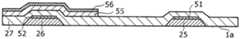
도 3은 본 발명에 따른 박막 트랜지스터 기판의 바람직한 실시양태를 예시하는 개략적인 단면도이다. 도 3에서, 도 2의 통상의 박막 트랜지스터 기판에 해당하는 부품은 동일한 도면 부호를 사용한다.3 is a schematic cross-sectional view illustrating a preferred embodiment of the thin film transistor substrate according to the present invention. In FIG. 3, components corresponding to the conventional thin film transistor substrate of FIG. 2 use the same reference numerals.
도 2 및 도 3의 비교에 의하면, 통상의 박막 트랜지스터 기판은 소스/드레인 전극 아래에 통상적으로 몰리브덴(Mo)으로 구성된 하부 장벽 금속층(53)을 포함한다(도 2)는 것을 나타내는 반면, 본 발명에 따른 박막 트랜지스터 기판은 하부 장벽 금속층(53)을 포함하지 않는다(도 3). 이러한 실시양태는 통상의 등가물과는 대조적으로, 하부 장벽 금속층의 개재 없이 알루미늄 합금 및 채널 무정형 규소 박막 사이의 직접적인 접속을 가능하게 한다. 이는 통상의 박막 트랜지스터 기판에 비해 동등 이상의 우수한 박막 트랜지스터 물성을 구현한다(하기의 실험예 1 및 2를 참조한다)2 and 3 show that a conventional thin film transistor substrate includes a lower barrier metal layer 53, typically composed of molybdenum (Mo), under the source / drain electrodes (FIG. 2). The thin film transistor substrate according to FIG. 3 does not include the lower barrier metal layer 53 (FIG. 3). This embodiment allows, in contrast to conventional equivalents, a direct connection between the aluminum alloy and the channel amorphous silicon thin film without intervening lower barrier metal layers. This realizes excellent thin film transistor physical properties equivalent to or higher than those of conventional thin film transistor substrates (see Experimental Examples 1 and 2 below).
도 3에 도시한 실시양태는 소스/드레인 배선에 배치된 상부 장벽 금속층(54)을 포함한다. 그러나, 상부 장벽 금속층(54)은 하기에서 설명한 본 발명의 제2의 실시양태에서와 같이 생략될 수 있다.The embodiment shown in FIG. 3 includes an upper
또한, 본 발명은 도 3에 도시한 박막 트랜지스터 기판에서 각각 주사선(25) 및 게이트 전극(26)에 배치된 장벽 금속층(51 및 52)의 필요성을 더욱 배제시킬 수 있다.Further, the present invention can further eliminate the need for the
결국, 본 발명은 통상의 배선에 필수적인 모든 장벽 금속층의 필요성을 배제시킬 수 있다.As a result, the present invention can eliminate the need for all barrier metal layers which are essential for normal wiring.
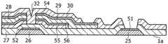
그 다음, 본 발명에 따른 도 3에 도시한 박막 트랜지스터 기판의 제조 방법은 도 4a 내지 도 4f를 참조하여 설명할 것이다. 2.0원자%의 니켈을 포함하는 Al-Ni 합금을 소스/드레인 전극으로서 사용하였다. 도 3의 부품에 해당하는 도 4a 내지 도 4f에서의 부품은 동일한 도면 부호를 사용하였다.Next, the method of manufacturing the thin film transistor substrate shown in FIG. 3 according to the present invention will be described with reference to FIGS. 4A to 4F. An Al-Ni alloy containing 2.0 atomic% nickel was used as the source / drain electrode. Parts in FIGS. 4A-4F corresponding to those in FIG. 3 used the same reference numerals.
우선, 두께가 약 250㎚인 알루미늄 합금 박막(Al-2.0원자% Nd)(61) 및 두께가 약 50㎚인 몰리브덴 박막(52)은 스퍼터링에 의하여 유리 기판(1a)상에 순차적으로 형성했다. 스퍼터링에 의한 성막은 실온에서 실시하였다. 다층 박막을 패턴화하여 게이트 전극(26) 및 주사선(25)을 형성하였다(도 4a). 이러한 공정에서, 다층 박막의 주위는 약 30° 내지 약 60 °의 각도에서 테이퍼 형태로 에칭시켜 도 4b에 도시된 그 다음의 단계에서 이의 표면에 형성하고자 하는 게이트 절연체(27)의 도포력을 개선시키는 것이 바람직하다.First, an aluminum alloy thin film (Al-2.0 atomic% Nd) 61 having a thickness of about 250 nm and a molybdenum
그 다음, 두께가 약 300㎚인 질화규소막(게이트 절연체)(27)를 통상적으로 플라즈마 CVD로 형성한다(도 4b). 본 명세서에서의 플라즈마 CVD에 의한 성막은 약 350℃의 온도에서 실시한다. 질화규소막(게이트 절연체)(27)상에는 두께가 약 200㎚인 미도핑된 수소화 무정형 규소막(a-Si-H)(55) 및, 통상적으로 플라즈마 CVD에 의한 두께 약 80㎚인 인-도핑된 n+-형 수소화 무정형 규소막(n+ a-Si-H)(56)을 순차적으로 형성했다. n+-형 수소화 무정형 규소막은 예를 들면 PH3의 특정의 분압을 포함하는 기체를 사용한 플라즈마 CVD를 실시하여 형성된다.Then, a silicon nitride film (gate insulator) 27 having a thickness of about 300 nm is typically formed by plasma CVD (FIG. 4B). The film formation by plasma CVD in this specification is performed at the temperature of about 350 degreeC. On the silicon nitride film (gate insulator) 27 is an undoped hydrogenated amorphous silicon film (a-Si-H) 55 having a thickness of about 200 nm and a phosphorus-doped typically about 80 nm thick by plasma CVD. An n+ -type hydrogenated amorphous silicon film (n+ a-Si-H) 56 was formed sequentially. The n+ -type hydrogenated amorphous silicon film is formed by performing plasma CVD using, for example, a gas containing a specific partial pressure of PH3 .
이렇게 형성된 수소화된 무정형 규소막(55) 및 n+-형 수소화된 무정형 규소막(56)을 패턴화하였다(도 4c).The hydrogenated
그 다음, 두께가 약 300㎚인 Al-2.0원자% Ni 합금막 및 두께가 약 50㎚인 몰리브덴막(54)을 스퍼터링에 의하여 순차적으로 형성했다(도 4d). 스퍼터링에 의한 성막은 실온에서 실시하였다. 이러한 실시양태에 의하면, 통상의 등가물에서의 전류에 실질적으로 해당하는 오프 상태의 전류는 하부 장벽 금속층의 개재 없이도 달성될 수 있다. 통상의 등가물에서, 몰리브덴의 하부 장벽 금속층은 무정형 규소 박막의 아래에 배치된다. 이러한 실시양태에서, 몰리브덴막(54)은 Al-2.0원자% Ni 합금막에 배치된다. 그러나, 몰리브덴막(54)은 하기의 제2의 실시양태에서와 같이 생략될 수 있다.Then, an Al-2.0 atomic% Ni alloy film having a thickness of about 300 nm and a
그후, 다층 박막을 패턴화하여 소스 전극(28) 및 드레인 전극(29)을 형성한다(도 4d). n+-형 수소화 무정형 규소막(56)은 마스크로서 소스 전극(28) 및 드레인 전극(29)을 사용한 건식 에칭에 의하여 스트리핑 처리하였다(도 4d).Thereafter, the multilayer thin film is patterned to form a
질화규소막(보호막)(30)은 통상적으로 플라즈마 CVD 시스템에서 약 300㎚의 두께로 형성했다(도 4e). 본 명세서에서의 성막은 약 200℃의 온도에서 실시하였다. 그후, 질화규소막(30)을 건식 에칭으로 처리하여 접촉 홀(57)을 형성하였다.The silicon nitride film (protective film) 30 was typically formed to a thickness of about 300 nm in a plasma CVD system (FIG. 4E). The film formation in this specification was performed at the temperature of about 200 degreeC. Thereafter, the
그 다음, 통상적으로 산소 플라즈마를 사용한 애싱(ashing) 단계를 실시하고, 포토레지스트층(도시하지 않음)은 예를 들면 아민을 포함하는 제거제를 사용하여 스트리핑 처리하였다. ITO 막(10 중량%의 주석 산화물을 추가로 포함하는 인듐 산화물)을 약 50㎚의 두께로 형성했다. 그 다음, 습식 에칭에 의한 패턴화를 실시하여 투명 화소 전극(5)을 생성하였다. 그리하여 박막 트랜지스터 기판을 완성하였다.Then, an ashing step using an oxygen plasma is usually performed, and the photoresist layer (not shown) is stripped using, for example, a remover containing an amine. An ITO film (indium oxide further comprising 10 wt% tin oxide) was formed to a thickness of about 50 nm. Then, patterning by wet etching was performed to produce the
본 명세서에서 투명 화소 전극(5)은 ITO 막이지만, 이는 IZO 막이 될 수도 있다. 무정형 규소 대신에 폴리규소(다결정질 규소)를 활성 반도체층으로서 사용할 수 있다.In the present specification, the
도 1에 도시된 액정 표시 디바이스는, 예를 들면 하기와 같은 방법으로 상기에서 제조한 박막 트랜지스터 기판을 사용하여 제조된다.The liquid crystal display device shown in FIG. 1 is manufactured using the thin film transistor substrate manufactured above by the following method, for example.
우선, 정렬층은 예를 들면 폴리아미드의 막을 박막 트랜지스터 기판(1)에 적용하고, 막을 건조시키고, 이를 러빙(rubbing)시켜 형성하였다.First, the alignment layer was formed by applying, for example, a film of polyamide to the thin
대향 기판(2)의 경우, 예를 들면 매트릭스로서 크롬을 패턴화하여 유리 기판상에 차광막(9)을 형성한다. 그 다음, 매트릭스 형상의 차광막(9)에서의 간극에는 적색, 녹색 및 청색 수지상 컬러 필터(8)를 형성한다. ITO 막과 같은 투명 전도성 막이 차광막(9) 및 컬러 필터(8)상의 공통 전극(7)으로서 형성된다. 그리하여 대향 전극이 제공된다. 그 후, 예를 들면 대향 전극의 최상층에 폴리이미드 막을 적용하고, 생성된 막을 건조 및 러빙시켜 정렬층(11)을 형성한다.In the case of the opposing board |
그후, 박막 트랜지스터 기판(1) 및 대향 기판(2)은, 대향 기판(2)의 정렬층(11) 및 박막 트랜지스터 기판(1)의 TFT를 서로 대면하도록 박막 트랜지스터 기판(1) 및 대향 기판(2)을 배치한다. 수지와 같은 밀봉재(16)를 사용하여 액정을 위한 충전 포트를 제외하고 2개의 기판을 접착시킨다. 이러한 공정에서, 박막 트랜지스터 기판(1)과 대향 기판(2) 사이의 거리(간극)는 예를 들면 이들 사이에 스페이서(15)를 삽입하여 실질적으로 일정하게 유지한다.Thereafter, the thin
이렇게 형성된 빈 셀을 진공하에 두고, 충전 포트를 액정 물질에 침지시키면서 압력을 대기압으로 점진적으로 증가시켜, 상기 빈 셀에 액정 물질을 충전시켜 액정 층을 형성한다. 마지막으로, 편광판(10)을 셀의 양면에 부착시켜 액정 표시 패널을 완성하였다.The empty cell thus formed is placed under vacuum and the pressure is gradually increased to atmospheric pressure while the filling port is immersed in the liquid crystal material to fill the empty cell with a liquid crystal material to form a liquid crystal layer. Finally, the polarizing plate 10 was attached to both sides of the cell to complete the liquid crystal display panel.
그 다음, 구동 회로(13)를 액정 표시 패널에 전기 접속시키고, 액정 표시 디바이스를 구동시키도록 액정 표시 패널(도 1)의 측면 또는 이면상에 배치한다. 액 정 표시 패널의 스크린이 되는 개방구를 갖는 프레임(23), 평면 광원으로서 배광체(22), 광도파로(20) 및 또다른 프레임(23)은 액정 표시 패널을 유지하도록 배치하여 액정 표시 디바이스를 완성하게 된다.Then, the
제2의 실시양태Second embodiment
제2의 실시양태에 따른 박막 트랜지스터 기판은, 상부 장벽 금속층(54) 및 하부 장벽 금속층(53) 모두를 배치하지 않은 것을 제외하고는 도 2에 도시한 바와 같은 제1의 실시양태에 따른 박막 트랜지스터 기판과 동일한 구조를 갖는다. 제1의 실시양태에 따른 박막 트랜지스터 기판은 하부 장벽 금속층(53)을 포함하지는 않지만, 상부 장벽 금속층(54)은 포함한다.The thin film transistor substrate according to the second embodiment is the thin film transistor according to the first embodiment as shown in FIG. 2 except that neither the upper
제2의 실시양태에 따른 박막 트랜지스터 기판은, 유리 기판(1a)상에서 두께가 300㎚인 알루미늄 합금 박막(Al-2.0원자% Nd)만을 형성하고 몰리브덴막은 형성하지 않은 것을 제외하고, 제1의 실시양태의 절차에 의하여 생성할 수 있다. 제2의 실시양태에 따른 박막 트랜지스터 기판에서, Al-Ni 합금 박막은 무정형 규소 박막뿐 아니라 투명 화소 전극에도 직접 접속시킨다. 이러한 실시양태는 실험예 3 및 4에서 입증한 바와 같이, 투명 화소 전극에 접속시키고자 하는 배선의 상부 장벽 금속층의 필요성을 배제시킬 뿐 아니라, 통상의 박막 트랜지스터 기판에 해당하거나 또는 이보다 우수한 양호한 박막 트랜지스터 물성을 얻을 수 있다.The thin film transistor substrate according to the second embodiment is the first embodiment except that only the aluminum alloy thin film (Al-2.0 atomic% Nd) having a thickness of 300 nm is formed on the
실시예Example
실험예Experimental Example 1 One
실험예 1 및 하기의 실험예 2는, 예를 들면 제1의 실시양태에 따른 박막 트랜지스터 기판을 사용하여 하부 장벽 금속층을 사용하지 않을 때조차 우수한 박막 트랜지스터 성질을 얻을 수 있다는 것을 입증하도록 실시하였다. Al-2.0원자% Ni 합금을 실험예 1 및 2에서의 소스/드레인 전극으로 사용하였으며, 이러한 합금 박막을 하기에서는 "Al-Ni 합금 박막"으로 지칭한다.Experimental Example 1 and Experimental Example 2 below were conducted to demonstrate that excellent thin film transistor properties can be obtained even when the lower barrier metal layer is not used, for example, using the thin film transistor substrate according to the first embodiment. An Al-2.0 atomic% Ni alloy was used as the source / drain electrode in Experimental Examples 1 and 2, and this alloy thin film is referred to as "Al-Ni alloy thin film" below.
이러한 실험예에서, 니켈 농화층 및 알루미늄 산화물 막의 니켈 함량, 두께 는 각각 RF 글로우 방전 방사 스펙트럼(GD-OES) 및 횡단면 투과형 전자 현미경 사진에서의 관찰에 의하여 측정한다. 니켈 농화층의 니켈 함량 및 알루미늄 산화물막에서의 산소 함량은 EDX에 의한 횡단면 투과형 전자 현미경 사진의 조성 분석에 의하여 측정한다.In this experimental example, the nickel content and thickness of the nickel thickened layer and the aluminum oxide film were measured by observation in an RF glow discharge emission spectrum (GD-OES) and a cross-sectional transmission electron micrograph, respectively. The nickel content of the nickel thickened layer and the oxygen content in the aluminum oxide film are measured by compositional analysis of the cross-sectional transmission electron micrograph by EDX.
무정형 규소 박막 및Amorphous silicon thin film andAlAl--NiNi 합금 박막 사이의 계면에서의 관찰 Observation at the interface between alloy thin films
우선, 본 발명에 따른 소스/드레인 전극용 무정형 규소 박막 및 Al-Ni 합금 박막 사이의 계면의 부근에서의 전기 전도율이 우수한 니켈 농화층의 존재가 검출되었다. 이는 박막 트랜지스터 기판의 순차적인 제조 공정을 참조하여 입증된다.First, the presence of the nickel thickening layer excellent in the electrical conductivity in the vicinity of the interface between the amorphous silicon thin film for the source / drain electrode and the Al-Ni alloy thin film according to the present invention was detected. This is demonstrated with reference to the sequential fabrication process of thin film transistor substrates.
상세하게는, 실온에서 무정형 규소 박막상에서의 Al-Ni 합금 박막의 형성 직후 계면의 부근을 관찰하였다. 도 5a 및 도 5b는 본 발명의 제1의 실시양태에 따른 실온에서의 무정형 규소 박막상에서의 Al-Ni 합금의 형성 직후 Al-Ni 합금 박막과 무정형 규소 박막 사이의 계면의 횡단면 투과형 전자 현미경 사진(횡단면 TEM) 및 고각 환형 암시야 주사 투과형 전자 현미경 사진(HAADF-STEM)을 각각 도시한다. 횡단면 투과형 전자 현미경 사진에 의하면 계면의 조성을 규명하며, HAADF-STEM은 니켈의 분포를 나타낸다.In detail, the vicinity of the interface was observed immediately after formation of the Al—Ni alloy thin film on the amorphous silicon thin film at room temperature. 5A and 5B are cross-sectional transmission electron micrographs of an interface between an Al—Ni alloy thin film and an amorphous silicon thin film immediately after formation of an Al—Ni alloy on an amorphous silicon thin film at room temperature according to a first embodiment of the present invention. Cross-sectional TEM) and elevation annular dark field scanning transmission electron micrographs (HAADF-STEM), respectively. The cross-sectional transmission electron micrographs reveal the composition of the interface, and HAADF-STEM shows the distribution of nickel.
도 5a는 Al-Ni 합금 박막이 원주형 입자 경계면을 갖는 것을 나타낸다. 계면은 EDX(에너지 분산형 X선 분광학)에 의하여 분석하여 규소와 알루미늄의 사이에는 상호확산이 존재하지 않는 것으로 관찰된 것으로 밝혀졌다.5A shows that the Al—Ni alloy thin film has a columnar grain boundary. The interface was analyzed by EDX (energy dispersive X-ray spectroscopy) and found that no interdiffusion exists between silicon and aluminum.
도 5b에서 화살표로 표시한 밝은 부분이 니켈이다. 상세하게는, 무정형 규소 박막상의 Al-Ni 합금 박막의 형성 직후조차도 표면에서 Al-Ni 합금 박막에서 니켈이 감소되었다.The bright part indicated by the arrow in FIG. 5B is nickel. Specifically, even after the formation of the Al—Ni alloy thin film on the amorphous silicon thin film, nickel was reduced in the Al—Ni alloy thin film at the surface.
그 다음, 박막 트랜지스터 기판의 제조 공정 완료후 무정형 규소 박막과 Al-Ni 합금 박막 사이의 계면 부근을 관찰하였다. 도 6a 및 도 6b는 계면의 횡단면 투과형 전자 현미경 사진(횡단면 TEM) 및 고각 환형 암시야 주사 투과형 전자 현미경 사진(HAADF-STEM)을 각각 도시한다.Then, after completion of the manufacturing process of the thin film transistor substrate, the vicinity of the interface between the amorphous silicon thin film and the Al-Ni alloy thin film was observed. 6A and 6B show cross-sectional transmission electron micrographs (transverse cross-section TEM) and elevation annular dark field scanning transmission electron micrographs (HAADF-STEM) of an interface, respectively.
상기에서 설명한 바와 같이, 본 실시양태에 따른 박막 트랜지스터 기판을 제조하도록 무정형 규소 박막상에 Al-Ni 합금 박막의 형성후 각종 성막 단계를 실시한다. 이들 단계에서, 열 이력이 최고 온도에 도달하는 단계는 질화규소막(보호막)을 형성하는 단계로서, 상기 단계에서는 예열을 포함한 열 처리를 20 분간 200℃에서 수행한다.As described above, various film forming steps are performed after the formation of the Al—Ni alloy thin film on the amorphous silicon thin film to manufacture the thin film transistor substrate according to the present embodiment. In these steps, the step where the thermal history reaches the highest temperature is a step of forming a silicon nitride film (protective film), in which the heat treatment including preheating is performed at 200 ° C. for 20 minutes.
도 6a는 본 실시양태에 따른 기판중의 니켈이 성막 단계후조차도 이의 원주형 입자 경계를 유지한다는 것을 증명한다. 또한, 도 5a에서와 같이 무정형 규소 박막과 Al-Ni 합금 박막 사이의 계면은 평활하며, EDX 분석에 의하면 규소와 알루미늄 사이에는 상호확산이 존재하지 않는 것으로 관찰되었다.6A demonstrates that nickel in a substrate according to this embodiment retains its columnar grain boundaries even after the deposition step. In addition, as shown in FIG. 5A, the interface between the amorphous silicon thin film and the Al-Ni alloy thin film was smooth, and EDX analysis showed no interdiffusion between silicon and aluminum.
도 6b는 니켈 함유 석출물 또는 금속간 화합물이 계면에서 형성되었다는 것을 나타낸다.6B shows that nickel containing precipitates or intermetallic compounds were formed at the interface.
또한, 박막 트랜지스터 기판의 제조 단계의 완료후 무정형 규소 박막 및 Al-Ni 합금 박막 사이의 계면 부근에서의 니켈 농도의 분포는 RF 글로우 방전 방사 스펙트럼(GD-OES)에 의하여 측정한다. GD-OES에 의하면, 아르곤 글로우 방전에 의한 스퍼터링을 실시하고, 스퍼터링된 원소의 고유 발광을 측정하여 원소의 농도를 측정하였다. 실험예 1에서, 스퍼터링 부위는 직경이 3 ㎜인 부위이며, 직경이 3 ㎜인 2차원 공간에서의 평균 니켈 농도를 측정하였다. 결과를 도 7b에 도시하였다.In addition, the distribution of nickel concentration near the interface between the amorphous silicon thin film and the Al-Ni alloy thin film after completion of the manufacturing step of the thin film transistor substrate is measured by RF glow discharge emission spectrum (GD-OES). According to GD-OES, sputtering by argon glow discharge was performed, and the intrinsic luminescence of the sputtered element was measured to measure the concentration of the element. In Experimental Example 1, the sputtering site was a site having a diameter of 3 mm, and the average nickel concentration in the two-dimensional space having a diameter of 3 mm was measured. The results are shown in Figure 7b.
비교로서, 실온에서의 무정형 규소 박막상에서의 Al-Ni 합금 박막의 형성 직후 계면 부근에서의 니켈 농도 분포를 상기의 절차에 의하여 측정하였다. 결과를 도 7a에 도시하였다.As a comparison, the nickel concentration distribution in the vicinity of the interface immediately after formation of the Al—Ni alloy thin film on the amorphous silicon thin film at room temperature was measured by the above procedure. The results are shown in Figure 7a.
도 7a 및 도 7b를 비교하면, 계면 부근은 막 표면을 제외하고 Al-Ni 합금 박막의 형성 직후 실질적으로 균질한 니켈 농도를 갖지만, 니켈 농화층은 모든 성막 단계 완료후 계면의 부근에서 형성되는 것으로 입증되었다. 이러한 결과는 도 6b에 도시된 고각 환형 암시야 주사 투과형 전자 현미경 사진(HAADF-STEM)의 결과와 일치한다. 니켈 농화층은 아마도 석출된 Al3Ni 금속간 화합물을 포함한다. 상세하게는 니켈 농화층은 계면으로부터 50㎚ 이내의 Al-Ni 합금 박막에 형성되며, 최고 니켈 함량은 약 4.0원자%이다.7A and 7B, the vicinity of the interface has a substantially homogeneous nickel concentration immediately after formation of the Al—Ni alloy thin film except for the film surface, but the nickel thickening layer is formed in the vicinity of the interface after completion of all the deposition steps. Proven. This result is consistent with the results of the high angle annular dark field scanning transmission electron micrograph (HAADF-STEM) shown in FIG. 6B. The nickel thickened layer probably contains the precipitated Al3 Ni intermetallic compound. Specifically, the nickel thickening layer is formed in the Al-Ni alloy thin film within 50nm from the interface, the highest nickel content is about 4.0 atomic%.
박막 트랜지스터 물성Thin Film Transistor Properties
TFT 테스트 조각의 드레인 전류-게이트 전압에 대한 스위칭 양상을 측정하였다. 또한, 무정형 규소 박막으로의 알루미늄의 확산은 이러한 물성에 의하여 평가할 수 있다. 이러한 절차에서, 누출 전류 및 역치는 하기와 같은 방법으로 측정하였다. 누출 전류는 박막 트랜지스터가 오프 작동시 흐르는 전류(음의 전압이 게이트 전압에 적용될 경우의 드레인 전류)이고, 역치(게이트 전압)는 박막 트랜지스터가 온 작동시의 전압이다.The switching behavior for the drain current-gate voltage of the TFT test piece was measured. In addition, the diffusion of aluminum into the amorphous silicon thin film can be evaluated by this physical property. In this procedure, leakage current and threshold were measured in the following manner. The leakage current is the current flowing in the thin film transistor off operation (drain current when negative voltage is applied to the gate voltage), and the threshold (gate voltage) is the voltage in the thin film transistor on operation.
게이트 길이(L)가 3 ㎛이고, 게이프 폭(W)이 30 ㎛이고, 게이트 길이에 대한 게이트 폭의 비(W/L)가 10인 TFT 테스트 조각을 사용하여 드레인 전류 및 게이트 전압을 측정하였다. 측정시, 드레인 전압을 10 V로 조정하였다. 본 명세서에서 오프-상태 전류라는 것은 -5 V에서의 게이트 전압을 인가할 경우의 전류로서 정의하며, 역치는 드레인 전류가 10-8 A에 도달한 경우의 게이트 전압으로서 정의한다.Measure drain current and gate voltage using a TFT test piece with a gate length (L) of 3 μm, a gate width (W) of 30 μm, and a ratio of gate width to gate length (W / L) of 10 It was. In the measurement, the drain voltage was adjusted to 10V. In the present specification, the off-state current is defined as the current when the gate voltage at -5 V is applied, and the threshold is defined as the gate voltage when the drain current reaches 10-8 A.
참조 샘플로서, Al-Nd 합금 박막 및 상부 및 하부 몰리브덴 장벽 금속층을 포함하는 통상의 다층 소스/드레인 배선을 사용하여 박막 트랜지스터를 제조하였으며, 박막 트랜지스터의 물성을 측정하였다. 통상의 박막 트랜지스터는 오프-상태의 전류가 3×10-12A이며, 이러한 값을 기준치로 정의하였다. 기준값(3×10-11A 이하)보다 10 배 이하인 오프-상태 전류를 갖는 샘플은 "우수"로 평가하였으며, 이러한 범위보다 추가로 높은 오프-상태 전류를 갖는 샘플은 "불량"(우수하지 않음)으로 평가하였다.As a reference sample, a thin film transistor was fabricated using a conventional multilayer source / drain interconnect including an Al—Nd alloy thin film and upper and lower molybdenum barrier metal layers, and the physical properties of the thin film transistor were measured. A typical thin film transistor has an off-state current of 3 x 10-12 A, which is defined as a reference value. Samples with off-state current less than 10 times below the reference value (3 × 10⁻¹¹ A or less) were rated as “good”, and samples with off-state currents higher than this range were “bad” (not good). Was evaluated.
본 발명에 따른 박막 트랜지스터는 오프-상태 전류가 5×10-12A이며, 이는 실질적으로 Al-Nd 합금 박막 및 상부 및 하부 몰리브덴 장벽 금속층을 포함하는 통상의 다층 소스/드레인 배선을 사용한 기준 샘플의 값(3×10-12 A)에 실질적으로 상응한다. 이러한 실시양태에 따른 박막 트랜지스터는 역치가 0.45V이며, 이는 통상의 다층 배선을 사용한 기준 샘플의 값(0.45V)과 동일하다.The thin film transistor according to the present invention has an off-state current of 5 x 10-12 A, which is substantially equivalent to that of a reference sample using conventional multilayer source / drain interconnects comprising Al-Nd alloy thin films and upper and lower molybdenum barrier metal layers. Substantially corresponds to the value (3 × 10⁻¹² A). The thin film transistor according to this embodiment has a threshold of 0.45V, which is equivalent to the value of the reference sample (0.45V) using a conventional multilayer wiring.
이러한 결과는 본 실시양태에 따른 박막 트랜지스터 기판이 하부 장벽 금속층을 사용하지 않더라도 형성되며, 박막 트랜지스터 물성은 통상의 소스/드레인 배선을 사용한 박막 트랜지스터 기판의 값에 실질적으로 상응한다.This result is formed even if the thin film transistor substrate according to the present embodiment does not use the lower barrier metal layer, and the thin film transistor physical properties substantially correspond to the values of the thin film transistor substrate using conventional source / drain wiring.
비교예Comparative example 1 One
비교예로서 박막 트랜지스터 기판은 Al-2.0원자% Ni 합금 대신에 소스/드레인 배선으로서 순수한 알루미늄을 사용한 것을 제외하고, 제1의 실시양태의 절차에 의하여 제조하였다. 그 다음, 실험예 1의 절차에 의한 투과 전자 현미경하에서 소스/드레인 전극용 무정형 규소 박막 및 순수한 알루미늄 합금 박막 사이의 계면 부근을 관찰하였다.As a comparative example, a thin film transistor substrate was prepared by the procedure of the first embodiment except that pure aluminum was used as the source / drain wiring instead of the Al-2.0 atomic% Ni alloy. Next, the vicinity of the interface between the amorphous silicon thin film for the source / drain electrodes and the pure aluminum alloy thin film was observed under a transmission electron microscope according to the procedure of Experimental Example 1.
우선, 실온에서 무정형 규소 박막상의 순수한 알루미늄막의 형성 직후 계면의 부근을 관찰하였다. 도 8a 및 도 8b는 투과 전자 현미경 사진 및 이의 확대 현미경 사진(고배율)을 각각 도시하며, 이들은 계면의 횡단면을 나타낸다. 또한, EDX 분석의 결과를 도 8b에 도시한다.First, the vicinity of the interface was observed immediately after formation of the pure aluminum film on the amorphous silicon thin film at room temperature. 8A and 8B show transmission electron micrographs and their magnified micrographs (high magnifications), respectively, which show the cross section of the interface. Moreover, the result of EDX analysis is shown in FIG. 8B.
도 8a 및 도 8b에 의하면 순수한 알루미늄 박막은 입자 경계가 불규칙하다는 것을 알 수 있다. 계면의 EDX 분석에 의하면 알루미늄은 계면으로부터 약 10㎚ 이내에 무정형 규소 박막중에 약 10원자% 함량으로 존재하는 것으로 밝혀졌다. 상세하게는, 비교예 1에 의한 샘플은 무정형 규소 박막상의 순수한 알루미늄 박막의 형성 직후조차도 계면에서의 알루미늄 확산을 나타내었다.8A and 8B show that the pure aluminum thin film has irregular particle boundaries. EDX analysis of the interface revealed that aluminum was present in the amorphous silicon thin film in about 10 atomic percent within about 10 nm from the interface. Specifically, the sample according to Comparative Example 1 exhibited aluminum diffusion at the interface even immediately after the formation of the pure aluminum thin film on the amorphous silicon thin film.
그 다음, 박막 트랜지스터 기판의 제조를 위한 모든 성막 단계를 완료한 후 전술한 것과 동일한 방법으로 무정형 규소 박막 및 순수한 알루미늄 박막 사이의 계면의 부근을 관찰하였다. 도 9a는 계면의 횡단면 투과 전자 현미경 사진이며, 도 9b는 도 9a의 투과 전자 현미경 사진과 동일한 부분의 EDX 분석의 결과로서 맵핑 화상(규소 맵 및 알루미늄 맵)을 도시한다.Then, after completing all the deposition steps for manufacturing the thin film transistor substrate, the vicinity of the interface between the amorphous silicon thin film and the pure aluminum thin film was observed in the same manner as described above. FIG. 9A is a cross-sectional transmission electron micrograph of an interface, and FIG. 9B shows a mapping image (silicon map and aluminum map) as a result of EDX analysis of the same portion as the transmission electron micrograph of FIG. 9A.
도 9a는 알루미늄이 추가로 확산되며, 알루미늄과 규소 사이의 상호확산은 비교예 1에 의한 샘플에서의 모든 성막 단계의 완료후 계면의 부근에 발생한다는 것을 입증한다.9A further demonstrates that aluminum is further diffused and that interdiffusion between aluminum and silicon occurs near the interface after completion of all deposition steps in the sample according to Comparative Example 1. FIG.
상세하게, 도 9b에서의 규소 맵 및 알루미늄 맵에 의하면 알루미늄은 계면으로부터 약 100㎚ 이내의 무정형 규소층에 확산되며, 규소는 계면으로부터 약 250㎚ 이내의 순수한 알루미늄 박막에 확산되었다는 것을 나타낸다.Specifically, the silicon map and the aluminum map in FIG. 9B show that aluminum diffuses into the amorphous silicon layer within about 100 nm from the interface and silicon diffuses into the pure aluminum thin film within about 250 nm from the interface.
비교예 1에 의한 샘플의 박막 트랜지스터 물성을 실험예 1의 절차에 의하여 측정하였다. 박막 트랜지스터의 오프-상태 전류는 통상의 다층 배선을 사용한 기준 샘플의 오프-상태 전류(3×10-12 A)보다 훨씬 높은 1×10⁻⁸ A인 것으로 밝혀졌다. 또한, 박막 트랜지스터의 역치는 통상의 다층 배선을 사용한 기준 샘플의 역치(0.45 V)보다 훨씬 높은 2.5 V인 것으로 밝혀졌다.The thin film transistor physical properties of the sample according to Comparative Example 1 were measured by the procedure of Experimental Example 1. The off-state current of the thin film transistor was found to be 1 × 10⁻⁸ A, which is much higher than the off-state current (3 × 10⁻¹² A) of the reference sample using conventional multilayer wiring. In addition, the threshold of the thin film transistor was found to be 2.5 V, which is much higher than the threshold (0.45 V) of the reference sample using a conventional multilayer wiring.
이러한 결과에 의하면, 박막 트랜지스터가 순수한 알루미늄 소스/드레인 배선을 포함하기는 하지만 하부 장벽 금속층을 포함하지 않는 경우, 박막 트랜지스터는 실질적으로 스위칭 양상을 나타낼 수 없는 것으로 입증되었다. 따라서, 순수한 알루미늄 소스/드레인 배선을 사용한 박막 트랜지스터는 장벽 금속층을 지녀야만 한다.These results demonstrate that when the thin film transistor includes pure aluminum source / drain interconnects but does not include a lower barrier metal layer, the thin film transistor is substantially incapable of exhibiting switching behavior. Therefore, thin film transistors using pure aluminum source / drain wiring must have a barrier metal layer.
실험예Experimental Example 2 2
표 1에 도시한 다양한 니켈 함량을 갖는 Al-Ni 합금을 사용하여 박막 트랜지스터 샘플을 제조하였으며, 박막 트랜지스터 물성(오프-상태 전류 및 역치)이 Al-Ni 합금의 조성에 따라 어떻게 변경되는지는 실험예 1의 절차에 의하여 측정하였다. 또한, 하기 표 1에 도시한 바와 같은 다양한 함량의 La 또는 Nd를 제3의 성분으로 추가로 포함하는 Al-2.0원자% Ni 합금을 사용한 박막 트랜지스터를 생성하였으며, 이의 박막 트랜지스터 물성을 동일한 방법으로 측정하였다.The thin film transistor samples were prepared using Al-Ni alloys having various nickel contents shown in Table 1, and how the thin film transistor properties (off-state current and threshold value) were changed depending on the composition of the Al-Ni alloy. It measured by the procedure of 1. In addition, a thin film transistor using an Al-2.0 atomic% Ni alloy further including La or Nd of various contents as shown in Table 1 as a third component was produced, and the thin film transistor physical properties thereof were measured by the same method. It was.
비교용 샘플로서, Al-Ni 합금 대신에 순수한 알루미늄, Mo, Al - 1원자% Si 및 Al - 2원자% Si 각각을 사용하여 박막 트랜지스터를 생성하고, 이의 박막 트랜지스터 물성을 측정하였다.As a comparative sample, instead of the Al-Ni alloy, pure aluminum, Mo, Al-1 atomic% Si, and Al-2 atomic% Si were used to generate thin film transistors, and their thin film transistor physical properties were measured.
오프-상태 전류를 하기와 같은 방법으로 평가하였다. 기준 샘플로서, Al-Nd 합금 박막 및 상부 및 하부 몰리브덴 장벽 금속층을 포함하는 통상의 다층 소스/드레인 배선을 사용하여 박막 트랜지스터를 제조하고, TFT의 물성을 측정하였다. 기준 샘플의 오프-상태 전류는 3×10-12 A이고, 이 값을 기준값으로 정의하였다. 기준 값(3×10-12 A)의 10 배 이하의 오프-상태 전류를 갖는 샘플, 즉 오프-상태 전류가 3×10-11 A 이하인 샘플을 "우수"로 평가하였으며, 이러한 범위보다 추가로 높은 오프-상태 전류를 갖는 샘플을 "불량"으로 평가하였다.Off-state current was evaluated in the following manner. As a reference sample, a thin film transistor was fabricated using a conventional multilayer source / drain interconnect including an Al—Nd alloy thin film and upper and lower molybdenum barrier metal layers, and the physical properties of the TFTs were measured. The off-state current of the reference sample is 3 x 10-12 A, which is defined as the reference value. Samples with off-state currents of 10 times or less of the reference value (3 × 10-12 A), i.e. samples with off-state currents of 3 × 10-11 A or less, were evaluated as "good" and further beyond this range. Samples with high off-state currents were rated "bad."
역치에 관해서는 몰리브덴의 역치의 ±0.2 V 이내의 역치를 갖는 샘플을 "우수"로 평가하였으며, 이러한 범위를 초과하는 역치를 갖는 샘플을 "불량"으로 평가하였다.Regarding the threshold, a sample having a threshold within ± 0.2 V of the molybdenum threshold was evaluated as "good", and a sample having a threshold exceeding this range was evaluated as "bad".
오프-상태 전류 및 역치를 종합적으로 평가하여 오프-상태 전류 및 역치 모두가 우수한 샘플을 "우수"한 박막 트랜지스터 물성을 갖는 것으로 평가하고, 이들 2 가지의 물성중 1종 이상이 불량한 샘플을 "불량"한 박막 트랜지스터 물성을 갖는 것으로 평가하였다.Comprehensive evaluation of the off-state current and the threshold evaluates the sample having both excellent off-state current and the threshold as having "excellent" thin film transistor properties, and at least one of these two properties to "poor" the sample. "It was evaluated to have a thin film transistor physical properties.
열 안정성Thermal stability
실험예 2에 사용된 순수한 알루미늄 및 알루미늄 합금의 열 안정성을 하기와 같은 방법으로 평가하였다.The thermal stability of pure aluminum and aluminum alloy used in Experimental Example 2 was evaluated by the following method.
순수한 알루미늄 및 알루미늄 합금을 각각 포함하는 샘플 박막을 스퍼터링에 의하여 유리 기판상에 약 200㎚의 두께로 형성하였다. 10 ㎛ 라인 및 스페이스 패턴이 이들 샘플상에 형성되었다. 그 다음 샘플을 1×10⁻³ Torr 이하의 진공하에서 200℃에서 1 시간 동안 또는 1 시간 동안 300℃에서 열처리하였으며, 샘플 박막의 표면을 400 배율의 광학 현미경으로 관찰하였다. 1 ㎡당 1×10⁹ 개 초과의 힐록을 나타내는 샘플은 "불량"한 열 안정성을 갖는 것으로 평가하고, 이러한 범위 미만의 힐록을 갖는 샘플을 "우수"한 열 안정성을 갖는 것으로 평가하였다.A sample thin film comprising pure aluminum and aluminum alloy, respectively, was formed to a thickness of about 200 nm on the glass substrate by sputtering. 10 μm lines and space patterns were formed on these samples. The sample was then heat treated at 200 ° C. for 1 hour or 1 hour at 300 ° C. under a vacuum of 1 × 10⁻³ Torr or less, and the surface of the sample thin film was observed with an optical microscope at 400 magnification. Samples showing more than 1 × 10⁹ hillocks per square meter were evaluated to have “poor” thermal stability, and samples having hillocks below this range were evaluated to have “excellent” thermal stability.
결과를 하기 표 1에 기재하였다. 표 1에서의 %는 각각 원자%이다.The results are shown in Table 1 below. The percentages in Table 1 are each atomic%.

표 1에 도시된 바와 같이, 소스/드레인 전극으로서 0.1원자% 이상의 니켈을 포함하는 알루미늄 합금을 사용한 박막 트랜지스터는 우수한 박막 트랜지스터 물성을 갖는다.As shown in Table 1, a thin film transistor using an aluminum alloy containing 0.1 atom% or more of nickel as a source / drain electrode has excellent thin film transistor properties.
또한, 소스/드레인 전극으로서 0.1원자% 내지 2.0원자%의 La 또는 0.1원자% 내지 1.0원자%의 Nd를 추가로 포함하는 Al - 2.0원자% Ni 합금을 사용한 박막 트랜지스터는 우수한 박막 트랜지스터 물성 이외에 개선된 열 안정성을 갖는다.In addition, thin film transistors using an Al-2.0 atomic% Ni alloy further including 0.1 atomic% to 2.0 atomic% La or 0.1 atomic% to 1.0 atomic% Nd as source / drain electrodes have been improved in addition to excellent thin film transistor properties. Has thermal stability.
반대로, 순수한 알루미늄, Al - 1원자% Si 및 Al - 2원자% Si를 사용한 박막 트랜지스터는 박막 트랜지스터 물성 및 열 안정성에 있어서 상당히 불량하다.In contrast, thin film transistors using pure aluminum, Al-1 atomic% Si and Al-2 atomic% Si are considerably poor in thin film transistor properties and thermal stability.
실험예Experimental Example 3 3
실험예 3 및 하기의 실험예 4에서, 제2의 실시양태에 따른 박막 트랜지스터 기판이 하부 장벽 금속층 및 상부 장벽 금속층 모두를 사용하지 않더라도 우수한 박막 트랜지스터 물성을 산출할 수 있도록 하기와 같은 방법으로 테스트를 실시하였다.In Experimental Example 3 and Experimental Example 4 below, the thin film transistor substrate according to the second embodiment was tested in the following manner so that excellent thin film transistor physical properties could be calculated even without using both the lower barrier metal layer and the upper barrier metal layer. Was carried out.
박막 트랜지스터 물성Thin Film Transistor Properties
우선, 제2의 실시양태에 따른 박막 트랜지스터의 박막 트랜지스터 물성을 실험예 1의 절차에 의하여 측정하였다. 박막 트랜지스터는 오프-상태 전류가 4×10-12 A이며, 이는 통상의 소스/드레인 배선을 사용한 기준 샘플의 오프-상태 전류(3×10-12 A)에 실질적으로 상응한다는 것을 발견하였다. 박막 트랜지스터는 역치가 0.45 V이며, 이는 통상의 소스/드레인 배선 기준 샘플의 역치(0.45 V)와 동일하다는 것을 발견하였다.First, the thin film transistor physical properties of the thin film transistor according to the second embodiment were measured by the procedure of Experimental Example 1. Thin film transistors have been found to have an off-state current of4x10 -12 A, which corresponds substantially to the off-state current (3x10-12 A) of a reference sample using conventional source / drain wiring. Thin film transistors have a threshold of 0.45 V, which is equivalent to the threshold of 0.45 V of a typical source / drain wiring reference sample.
그 다음, Al - 2.0원자% Ni 합금 박막은 투명 화소 전극과 직접 접촉되며, 직접 접촉 저항(접촉 저항)을 하기와 같은 방법으로 측정하였다.Then, the Al-2.0 atomic% Ni alloy thin film was in direct contact with the transparent pixel electrode, and the direct contact resistance (contact resistance) was measured by the following method.
1) 인듐 산화물 및 10 중량%의 주석 산화물을 포함하는 인듐 주석 산화물(ITO)을 투명 화소 전극으로 사용하였다.1) Indium tin oxide (ITO) containing indium oxide and 10 wt% tin oxide was used as a transparent pixel electrode.
2) 3mTorr의 압력에서 분위기 기체로서 아르곤을 사용하여 두께 200㎚로 박막을 형성했다.2) A thin film was formed to a thickness of 200 nm using argon as an atmospheric gas at a pressure of 3 mTorr.
3) 가열은 200℃에서 20 분간 실시하였다.3) Heating was performed at 200 degreeC for 20 minutes.
4) 접촉 저항률의 측정4) Measurement of contact resistivity
도 10에 도시한 접촉 홀 크기가 10㎛2인 켈빈 패턴을 제조하고, 4-단자 측정을 실시하였다. 상세하게는, 2개의 단자를 사용하여 ITO(또는 IZO) 및 알루미늄 합금 사이에 전류를 통과시키고, ITO(또는 IZO) 및 알루미늄 합금 사이의 전압 강하는 다른 2개의 단자를 사용하여 측정하였다. 보다 상세하게는, 전류 I를 I1-I2 의 사이에 통과시키고, V1과 V2 사이의 전압 V를 측정하고(도 10), 접촉 C의 직접 접촉 저항률 R은 수학식
제2의 실시양태에 따른 박막 트랜지스터는 접촉 저항률이 8×10⁻⁵Ω·㎠ 이하이어서 우수한 박막 트랜지스터 물성을 갖는 것으로 밝혀졌다.The thin film transistor according to the second embodiment has been found to have excellent thin film transistor physical properties because the contact resistivity is 8 × 10⁻⁵ Pa ·
ITO 막(투명 화소 전극)과 Al-Ni 합금 박막 사이의 계면의 관찰Observation of the interface between the ITO film (transparent pixel electrode) and the Al-Ni alloy thin film
그 다음, 횡단면 투과 전자 현미경 사진을 촬영하여 ITO 막과 Al-Ni 합금 박막 사이의 계면을 관찰하고, 계면 부근에서의 조성을 EDS로 분석하였다. 결과를 도 11에 도시하였다.Then, a cross-sectional transmission electron micrograph was taken to observe the interface between the ITO film and the Al-Ni alloy thin film, and the composition near the interface was analyzed by EDS. The results are shown in FIG.
도 11은 두께가 약 5㎚인 알루미늄 산화물(AlOx)을 포함하는 전기 전도성층이 계면에 형성된 것으로 나타났다. 또한, 두께가 약 1㎚인 니켈 농화층이 전기 전도성 AlOx 층과 체적이 큰 Al-Ni 합금 박막 사이의 계면에 형성되었다. 니켈 농화층은 니켈 함량이 약 8원자%이었다. 이는 아마도 알루미늄은 산화물 막에 확산되지만, 니켈은 알루미늄의 산화를 진행시켜 체적내로 확산되지 못하며, 니켈은 접촉 홀의 건식 에칭시 알루미늄보다 잔류물로서 잔존하는 경향이 추가로 크기 때문일 것이다. 이러한 결과로서 형성된 니켈 농화층은 알루미늄 합금 거체로부터 알루미늄 이온의 확산을 방지하는 역할을 한다. 그래서, 알루미늄 산화를 효과적으로 방지할 수 있다.11 shows that an electrically conductive layer including aluminum oxide (AlOx ) having a thickness of about 5 nm is formed at the interface. In addition, a nickel thickened layer having a thickness of about 1 nm was formed at the interface between the electrically conductive AlOx layer and the bulk Al-Ni alloy thin film. The nickel thick layer had a nickel content of about 8 atomic percent. This is probably because aluminum diffuses into the oxide film, but nickel proceeds to oxidize aluminum and does not diffuse into the volume, and nickel is more likely to remain as a residue than aluminum during dry etching of contact holes. The nickel thickening layer formed as a result of this serves to prevent the diffusion of aluminum ions from the aluminum alloy giant. Thus, aluminum oxidation can be effectively prevented.
실험예Experimental Example 4 4
박막 트랜지스터 샘플은 하기 표 2에 기재한 여러 가지의 니켈 함량을 갖는 Al-Ni 합금을 사용하여 제조하였으며, 박막 트랜지스터 물성(오프-상태 전류 및 역치)이 Al-Ni 합금의 조성에 따라서 어떻게 변경되는지는 실험예 3의 절차에 의하여 측정하였다. 또한, 하기 표 2에 기재한 바와 같은 여러 가지 함량의 La 또는 Nd를 제3의 성분으로서 추가로 포함하는 Al - 2.0원자% Ni 합금을 사용한 박막 트랜지스터를 제조하고, 이의 박막 트랜지스터 물성을 동일한 방법으로 측정하였다.The thin film transistor samples were prepared using Al-Ni alloys having various nickel contents shown in Table 2 below, and how the thin film transistor properties (off-state current and threshold) were changed depending on the composition of the Al-Ni alloy. Was measured by the procedure of Experimental Example 3. In addition, a thin film transistor using an Al-2.0 atomic% Ni alloy further including various contents of La or Nd as a third component as described in Table 2 was prepared, and the thin film transistor physical properties thereof were prepared in the same manner. Measured.
비교용 샘플로서, Al-Ni 합금 대신에 순수한 알루미늄, Mo, Al - 1원자% Si 및 Al - 2.0원자% Si를 각각 사용하여 박막 트랜지스터를 제조하고, 이의 박막 트랜지스터 물성을 측정하였다. 오프-상태 전류의 기준은 실험예 2와 동일하다. 결과를 하기 표 2에 기재하였다.As a comparative sample, instead of the Al-Ni alloy, pure aluminum, Mo, Al-1 atomic% Si, and Al-2.0 atomic% Si were used to prepare a thin film transistor, and the thin film transistor physical properties thereof were measured. The criterion of the off-state current is the same as in

표 2에 도시한 바에 의하면, 소스/드레인 전극으로서 0.1원자% 이상의 니켈을 포함하는 알루미늄 합금을 사용한 박막 트랜지스터는 박막 트랜지스터 물성이 우수하다.As shown in Table 2, the thin film transistor using aluminum alloy containing 0.1 atomic% or more of nickel as a source / drain electrode has excellent thin film transistor physical properties.
또한, 0.1원자% 내지 2.0원자%의 La 또는 0.1원자% 내지 1.0원자%의 Nd를 추가로 포함하는 Al-2.0원자% Ni 합금을 사용한 박막 트랜지스터는 박막 트랜지스터 물성이 우수하다.Further, the thin film transistor using Al-2.0 atomic% Ni alloy further comprising 0.1 atomic% to 2.0 atomic% La or 0.1 atomic% to 1.0 atomic% Nd has excellent thin film transistor physical properties.
반대로, 순수한 알루미늄, Al - 1원자% Si 및 Al - 2원자% Si를 사용한 박막 트랜지스터는 박막 트랜지스터 물성이 상당히 불량하다.In contrast, thin film transistors using pure aluminum, Al-1 atomic% Si, and Al-2 atomic% Si are quite poor in thin film transistor properties.
본 발명에 따른 박막 트랜지스터 기판은 열 안정성 및 박막 트랜지스터 물성이 우수하다.The thin film transistor substrate according to the present invention has excellent thermal stability and thin film transistor physical properties.
Claims (27)
Translated fromKoreanPriority Applications (1)
| Application Number | Priority Date | Filing Date | Title |
|---|---|---|---|
| KR1020060077057AKR100799824B1 (en) | 2005-08-17 | 2006-08-16 | Source / drain electrodes, transistor substrates and methods of manufacturing the same, and display devices |
Applications Claiming Priority (2)
| Application Number | Priority Date | Filing Date | Title |
|---|---|---|---|
| JPJP-P-2005-00236993 | 2005-08-17 | ||
| KR1020060077057AKR100799824B1 (en) | 2005-08-17 | 2006-08-16 | Source / drain electrodes, transistor substrates and methods of manufacturing the same, and display devices |
Publications (2)
| Publication Number | Publication Date |
|---|---|
| KR20070021067A KR20070021067A (en) | 2007-02-22 |
| KR100799824B1true KR100799824B1 (en) | 2008-01-31 |
Family
ID=41339224
Family Applications (1)
| Application Number | Title | Priority Date | Filing Date |
|---|---|---|---|
| KR1020060077057AExpired - Fee RelatedKR100799824B1 (en) | 2005-08-17 | 2006-08-16 | Source / drain electrodes, transistor substrates and methods of manufacturing the same, and display devices |
Country Status (1)
| Country | Link |
|---|---|
| KR (1) | KR100799824B1 (en) |
Cited By (1)
| Publication number | Priority date | Publication date | Assignee | Title |
|---|---|---|---|---|
| WO2024167046A1 (en)* | 2023-02-10 | 2024-08-15 | 주식회사 큐프럼 머티리얼즈 | Thin film transistor electrode, and alloy composition comprising aluminum, manganese, titanium, and silicon for reflective electrode |
Families Citing this family (1)
| Publication number | Priority date | Publication date | Assignee | Title |
|---|---|---|---|---|
| CN118082383B (en)* | 2024-03-01 | 2025-10-03 | 山东华菱电子股份有限公司 | Thin film thermal print head and manufacturing method thereof |
Citations (4)
| Publication number | Priority date | Publication date | Assignee | Title |
|---|---|---|---|---|
| JPS59193062A (en) | 1983-04-15 | 1984-11-01 | Hitachi Ltd | Polycrystalline silicon thin film transistor |
| KR20040080531A (en)* | 2003-03-12 | 2004-09-20 | 삼성에스디아이 주식회사 | Thin film transistor and flat display device comprising it |
| KR20040080895A (en)* | 2003-03-12 | 2004-09-20 | 삼성에스디아이 주식회사 | Thin film transistor and flat display device comprising it |
| KR20060055015A (en)* | 2004-11-17 | 2006-05-23 | 삼성전자주식회사 | Method of manufacturing thin film transistor, thin film transistor and display substrate using same |
- 2006
- 2006-08-16KRKR1020060077057Apatent/KR100799824B1/ennot_activeExpired - Fee Related
Patent Citations (4)
| Publication number | Priority date | Publication date | Assignee | Title |
|---|---|---|---|---|
| JPS59193062A (en) | 1983-04-15 | 1984-11-01 | Hitachi Ltd | Polycrystalline silicon thin film transistor |
| KR20040080531A (en)* | 2003-03-12 | 2004-09-20 | 삼성에스디아이 주식회사 | Thin film transistor and flat display device comprising it |
| KR20040080895A (en)* | 2003-03-12 | 2004-09-20 | 삼성에스디아이 주식회사 | Thin film transistor and flat display device comprising it |
| KR20060055015A (en)* | 2004-11-17 | 2006-05-23 | 삼성전자주식회사 | Method of manufacturing thin film transistor, thin film transistor and display substrate using same |
Cited By (1)
| Publication number | Priority date | Publication date | Assignee | Title |
|---|---|---|---|---|
| WO2024167046A1 (en)* | 2023-02-10 | 2024-08-15 | 주식회사 큐프럼 머티리얼즈 | Thin film transistor electrode, and alloy composition comprising aluminum, manganese, titanium, and silicon for reflective electrode |
Also Published As
| Publication number | Publication date |
|---|---|
| KR20070021067A (en) | 2007-02-22 |
Similar Documents
| Publication | Publication Date | Title |
|---|---|---|
| US7683370B2 (en) | Source/drain electrodes, transistor substrates and manufacture methods, thereof, and display devices | |
| KR100983196B1 (en) | Thin Film Transistor Substrates and Display Devices | |
| KR100600229B1 (en) | An electronic device and a method for producing the same, and a sputtering target | |
| KR101124831B1 (en) | Display device, process for producing the display device, and sputtering target | |
| KR100802879B1 (en) | Display device | |
| KR101085271B1 (en) | Alloy alloy film, display device and sputtering target for display device | |
| KR20080084790A (en) | Display devices and their sputtering targets for manufacturing | |
| JP2007081385A (en) | Source drain electrode, transistor substrate and method for manufacturing the same, and display device | |
| US20110147753A1 (en) | Display device, copper alloy film for use therein, and copper alloy sputtering target | |
| KR20080114573A (en) | Display device and manufacturing method of display device | |
| WO2010053135A1 (en) | Al alloy film for display device, display device and sputtering target | |
| JP2009105424A (en) | Thin-film transistor substrate, and display device | |
| KR100851131B1 (en) | Source/drain electrodes, thin-film transistor substrates, manufacture methods thereof, and display devices | |
| JP5374111B2 (en) | Display device and Cu alloy film used therefor | |
| KR100799824B1 (en) | Source / drain electrodes, transistor substrates and methods of manufacturing the same, and display devices | |
| CN101828212B (en) | Display device and cu alloy film for use in the display device | |
| TW200914971A (en) | Display device and sputtering target | |
| US8558248B2 (en) | A1 alloy film, electronic device, and active matrix substrate for use in electrooptic display device | |
| JP4886285B2 (en) | Display device | |
| JP5096522B2 (en) | Display device | |
| JP2008124483A (en) | Thin-film transistor substrate, and display device |
Legal Events
| Date | Code | Title | Description |
|---|---|---|---|
| A201 | Request for examination | ||
| PA0109 | Patent application | St.27 status event code:A-0-1-A10-A12-nap-PA0109 | |
| PA0201 | Request for examination | St.27 status event code:A-1-2-D10-D11-exm-PA0201 | |
| P11-X000 | Amendment of application requested | St.27 status event code:A-2-2-P10-P11-nap-X000 | |
| P13-X000 | Application amended | St.27 status event code:A-2-2-P10-P13-nap-X000 | |
| R15-X000 | Change to inventor requested | St.27 status event code:A-3-3-R10-R15-oth-X000 | |
| R16-X000 | Change to inventor recorded | St.27 status event code:A-3-3-R10-R16-oth-X000 | |
| PG1501 | Laying open of application | St.27 status event code:A-1-1-Q10-Q12-nap-PG1501 | |
| D13-X000 | Search requested | St.27 status event code:A-1-2-D10-D13-srh-X000 | |
| D14-X000 | Search report completed | St.27 status event code:A-1-2-D10-D14-srh-X000 | |
| E902 | Notification of reason for refusal | ||
| PE0902 | Notice of grounds for rejection | St.27 status event code:A-1-2-D10-D21-exm-PE0902 | |
| E13-X000 | Pre-grant limitation requested | St.27 status event code:A-2-3-E10-E13-lim-X000 | |
| P11-X000 | Amendment of application requested | St.27 status event code:A-2-2-P10-P11-nap-X000 | |
| P13-X000 | Application amended | St.27 status event code:A-2-2-P10-P13-nap-X000 | |
| E701 | Decision to grant or registration of patent right | ||
| PE0701 | Decision of registration | St.27 status event code:A-1-2-D10-D22-exm-PE0701 | |
| GRNT | Written decision to grant | ||
| PR0701 | Registration of establishment | St.27 status event code:A-2-4-F10-F11-exm-PR0701 | |
| PR1002 | Payment of registration fee | St.27 status event code:A-2-2-U10-U11-oth-PR1002 Fee payment year number:1 | |
| PG1601 | Publication of registration | St.27 status event code:A-4-4-Q10-Q13-nap-PG1601 | |
| G170 | Re-publication after modification of scope of protection [patent] | ||
| PG1701 | Publication of correction | St.27 status event code:A-5-5-P10-P19-oth-PG1701 Patent document republication publication date:20080421 Republication note text:Request for Correction Notice (Document Request) Gazette number:1007998240000 Gazette reference publication date:20080131 | |
| PR1001 | Payment of annual fee | St.27 status event code:A-4-4-U10-U11-oth-PR1001 Fee payment year number:4 | |
| PR1001 | Payment of annual fee | St.27 status event code:A-4-4-U10-U11-oth-PR1001 Fee payment year number:5 | |
| FPAY | Annual fee payment | Payment date:20121220 Year of fee payment:6 | |
| PR1001 | Payment of annual fee | St.27 status event code:A-4-4-U10-U11-oth-PR1001 Fee payment year number:6 | |
| R18-X000 | Changes to party contact information recorded | St.27 status event code:A-5-5-R10-R18-oth-X000 | |
| FPAY | Annual fee payment | Payment date:20131219 Year of fee payment:7 | |
| PR1001 | Payment of annual fee | St.27 status event code:A-4-4-U10-U11-oth-PR1001 Fee payment year number:7 | |
| PN2301 | Change of applicant | St.27 status event code:A-5-5-R10-R13-asn-PN2301 St.27 status event code:A-5-5-R10-R11-asn-PN2301 | |
| FPAY | Annual fee payment | Payment date:20150106 Year of fee payment:8 | |
| PR1001 | Payment of annual fee | St.27 status event code:A-4-4-U10-U11-oth-PR1001 Fee payment year number:8 | |
| FPAY | Annual fee payment | Payment date:20151217 Year of fee payment:9 | |
| PR1001 | Payment of annual fee | St.27 status event code:A-4-4-U10-U11-oth-PR1001 Fee payment year number:9 | |
| FPAY | Annual fee payment | Payment date:20170102 Year of fee payment:10 | |
| PR1001 | Payment of annual fee | St.27 status event code:A-4-4-U10-U11-oth-PR1001 Fee payment year number:10 | |
| FPAY | Annual fee payment | Payment date:20180103 Year of fee payment:11 | |
| PR1001 | Payment of annual fee | St.27 status event code:A-4-4-U10-U11-oth-PR1001 Fee payment year number:11 | |
| FPAY | Annual fee payment | Payment date:20190103 Year of fee payment:12 | |
| PR1001 | Payment of annual fee | St.27 status event code:A-4-4-U10-U11-oth-PR1001 Fee payment year number:12 | |
| FPAY | Annual fee payment | Payment date:20200103 Year of fee payment:13 | |
| PR1001 | Payment of annual fee | St.27 status event code:A-4-4-U10-U11-oth-PR1001 Fee payment year number:13 | |
| PR1001 | Payment of annual fee | St.27 status event code:A-4-4-U10-U11-oth-PR1001 Fee payment year number:14 | |
| PC1903 | Unpaid annual fee | St.27 status event code:A-4-4-U10-U13-oth-PC1903 Not in force date:20220125 Payment event data comment text:Termination Category : DEFAULT_OF_REGISTRATION_FEE | |
| PC1903 | Unpaid annual fee | St.27 status event code:N-4-6-H10-H13-oth-PC1903 Ip right cessation event data comment text:Termination Category : DEFAULT_OF_REGISTRATION_FEE Not in force date:20220125 | |
| P22-X000 | Classification modified | St.27 status event code:A-4-4-P10-P22-nap-X000 |