KR100799786B1 - Method of manufacturing surface emission conversion element, liquid crystal display device and surface emission conversion element - Google Patents
Method of manufacturing surface emission conversion element, liquid crystal display device and surface emission conversion elementDownload PDFInfo
- Publication number
- KR100799786B1 KR100799786B1KR1020040013744AKR20040013744AKR100799786B1KR 100799786 B1KR100799786 B1KR 100799786B1KR 1020040013744 AKR1020040013744 AKR 1020040013744AKR 20040013744 AKR20040013744 AKR 20040013744AKR 100799786 B1KR100799786 B1KR 100799786B1
- Authority
- KR
- South Korea
- Prior art keywords
- conversion element
- radiation
- concave portion
- light
- dielectric constant
- Prior art date
- Legal status (The legal status is an assumption and is not a legal conclusion. Google has not performed a legal analysis and makes no representation as to the accuracy of the status listed.)
- Expired - Fee Related
Links
Images


Classifications
- B—PERFORMING OPERATIONS; TRANSPORTING
- B25—HAND TOOLS; PORTABLE POWER-DRIVEN TOOLS; MANIPULATORS
- B25J—MANIPULATORS; CHAMBERS PROVIDED WITH MANIPULATION DEVICES
- B25J15/00—Gripping heads and other end effectors
- B25J15/04—Gripping heads and other end effectors with provision for the remote detachment or exchange of the head or parts thereof
- B25J15/0408—Connections means
- B25J15/0433—Connections means having gripping members
- G—PHYSICS
- G02—OPTICS
- G02B—OPTICAL ELEMENTS, SYSTEMS OR APPARATUS
- G02B6/00—Light guides; Structural details of arrangements comprising light guides and other optical elements, e.g. couplings
- G02B6/0001—Light guides; Structural details of arrangements comprising light guides and other optical elements, e.g. couplings specially adapted for lighting devices or systems
- G02B6/0011—Light guides; Structural details of arrangements comprising light guides and other optical elements, e.g. couplings specially adapted for lighting devices or systems the light guides being planar or of plate-like form
- G02B6/0033—Means for improving the coupling-out of light from the light guide
- G02B6/0035—Means for improving the coupling-out of light from the light guide provided on the surface of the light guide or in the bulk of it
- G02B6/0036—2-D arrangement of prisms, protrusions, indentations or roughened surfaces
- B—PERFORMING OPERATIONS; TRANSPORTING
- B21—MECHANICAL METAL-WORKING WITHOUT ESSENTIALLY REMOVING MATERIAL; PUNCHING METAL
- B21D—WORKING OR PROCESSING OF SHEET METAL OR METAL TUBES, RODS OR PROFILES WITHOUT ESSENTIALLY REMOVING MATERIAL; PUNCHING METAL
- B21D37/00—Tools as parts of machines covered by this subclass
- B21D37/04—Movable or exchangeable mountings for tools
- G—PHYSICS
- G02—OPTICS
- G02B—OPTICAL ELEMENTS, SYSTEMS OR APPARATUS
- G02B6/00—Light guides; Structural details of arrangements comprising light guides and other optical elements, e.g. couplings
- G02B6/0001—Light guides; Structural details of arrangements comprising light guides and other optical elements, e.g. couplings specially adapted for lighting devices or systems
- G02B6/0011—Light guides; Structural details of arrangements comprising light guides and other optical elements, e.g. couplings specially adapted for lighting devices or systems the light guides being planar or of plate-like form
- G02B6/0033—Means for improving the coupling-out of light from the light guide
- G02B6/005—Means for improving the coupling-out of light from the light guide provided by one optical element, or plurality thereof, placed on the light output side of the light guide
- G02B6/0051—Diffusing sheet or layer
- G—PHYSICS
- G02—OPTICS
- G02B—OPTICAL ELEMENTS, SYSTEMS OR APPARATUS
- G02B6/00—Light guides; Structural details of arrangements comprising light guides and other optical elements, e.g. couplings
- G02B6/0001—Light guides; Structural details of arrangements comprising light guides and other optical elements, e.g. couplings specially adapted for lighting devices or systems
- G02B6/0011—Light guides; Structural details of arrangements comprising light guides and other optical elements, e.g. couplings specially adapted for lighting devices or systems the light guides being planar or of plate-like form
- G02B6/0033—Means for improving the coupling-out of light from the light guide
- G02B6/0058—Means for improving the coupling-out of light from the light guide varying in density, size, shape or depth along the light guide
- G02B6/0061—Means for improving the coupling-out of light from the light guide varying in density, size, shape or depth along the light guide to provide homogeneous light output intensity
Landscapes
- Physics & Mathematics (AREA)
- Engineering & Computer Science (AREA)
- Mechanical Engineering (AREA)
- General Physics & Mathematics (AREA)
- Optics & Photonics (AREA)
- Robotics (AREA)
- Planar Illumination Modules (AREA)
- Liquid Crystal (AREA)
- Light Guides In General And Applications Therefor (AREA)
Abstract
Translated fromKoreanDescription
Translated fromKorean도 1은 본원 발명의 일 실시 형태의 액정 표시 장치의 개요를 설명하기 위한 일부 단면을 포함하는 측면도.BRIEF DESCRIPTION OF THE DRAWINGS It is a side view containing some cross section for demonstrating the outline | summary of the liquid crystal display device of one Embodiment of this invention.
도 2는 도 1의 주요부 확대도.2 is an enlarged view of a main part of FIG. 1;
도 3은 동 실시 형태의 폐공간(오목부)의 배열을 설명하기 위한 단면 평면도.3 is a cross-sectional plan view for explaining the arrangement of a closed space (concave portion) of the embodiment.
도 4는 동 실시 형태에서 채용 가능한 폐공간(오목부)의 형상을 설명하기 위한 사시도.4 is a perspective view for explaining a shape of a closed space (concave portion) that can be employed in the embodiment.
도 5는 다른 실시 형태의 액정 표시 장치의 개요를 설명하기 위한 일부 단면을 포함하는 측면도.FIG. 5 is a side view including a partial cross section for explaining an outline of a liquid crystal display device of another embodiment. FIG.
도 6은 다른 실시 형태의 액정 표시 장치의 개요를 설명하기 위한 일부 단면을 포함하는 측면도.FIG. 6 is a side view including a partial cross section for explaining an outline of a liquid crystal display device of another embodiment. FIG.
도 7은 다른 실시 형태의 액정 표시 장치의 개요를 설명하기 위한 일부 단면을 포함하는 측면도.FIG. 7 is a side view including a partial cross section for explaining an outline of a liquid crystal display device of another embodiment; FIG.
도 8은 다른 실시 형태의 액정 표시 장치의 개요를 설명하기 위한 일부 단면 을 포함하는 측면도.8 is a side view including a partial cross section for explaining an outline of a liquid crystal display device of another embodiment.
도 9는 다른 실시 형태의 액정 표시 장치의 개요를 설명하기 위한 일부 단면을 포함하는 측면도.9 is a side view including a partial cross section for explaining an outline of a liquid crystal display device of another embodiment.
도 10은 다른 실시 형태의 액정 표시 장치의 개요를 설명하기 위한 일부 단면을 포함하는 측면도.FIG. 10 is a side view including a partial cross section for explaining an outline of a liquid crystal display device of another embodiment. FIG.
도 11은 종래예의 도광판의 개요를 설명하기 위한 설명도.11 is an explanatory diagram for illustrating an outline of a light guide plate of a conventional example.
〈도면의 주요 부분에 대한 부호의 설명〉<Explanation of symbols for main parts of drawing>
100 : 도광판100: light guide plate
101 : 소자 본체101: element body
103 : 폐공간103: closed space
121 : 오목부121: recess
123 : 출광면123: light exit surface
125 : 전반사 억제층125: total reflection suppression layer
200 : 광원200: light source
300 : 액정 표시 패널300: liquid crystal display panel
본원 발명은, 방사원으로부터 방사되는 전자파를 면방사로 변환하는 면방사 변환 소자에 관한 것이다. 보다 구체적으로는, 예를 들면 액정 표시 장치에서 이 용되어, 광원으로부터 방사되는 광을 면방사로 변환하는 도광판에 적합한 발명이다.The present invention relates to a surface radiation conversion element for converting electromagnetic waves radiated from a radiation source into surface radiation. More specifically, it is an invention suitable for the light guide plate used for the liquid crystal display device and converting the light radiate | emitted from a light source into surface radiation, for example.
종래, 액정 표시 장치에 있어서, 예를 들면 도광판은 측방에 광원이 설치됨과 함께 상면에 액정 변환 소자가 장치되고, 광원으로부터 방사된 광을 액정 표시 소자로 유도하기 위해서 이용된다.Background Art Conventionally, in a liquid crystal display device, for example, a light guide plate is provided with a light source on the side and a liquid crystal conversion element is provided on an upper surface thereof, and is used to guide light emitted from the light source to the liquid crystal display element.
여기서, 도광판은, 예를 들면 도 11에 도시한 바와 같이 표시면(출광면)의 반대면에 인쇄나 요철 처리 가공이 실시되어 있다. 그리고, 광원으로부터 방사된 광은 이 반대면에서 산란되어, 이 산란광 중 전반사각을 벗어난 각도의 광만이 출광면으로부터 출광되고 있다. 즉, 산란광 중 전반사각을 벗어나지 않은 광은, 출광면으로부터 출광되지 않고, 출광면에서 반사된다. 게다가, 전반사각을 벗어난 광도, 출광면으로부터 모두 출광하는 것은 아니다. 출광면에서 대부분의 광이 반사하여 내부로 회귀한다. 즉, 출광면으로부터 출광할 수 있는 광은, 반대면에서 인쇄나 요철에 충돌하여 산란한 광 중에서, 전반사각을 벗어난 광의 극히 일부라고 하는 얼마되지 않는 성분으로 되어 있다. 그 결과, 이와 같은 반사가 출광까지 반복되어 광로가 길어짐으로써, 광은 감쇠되고, 그 때문에 광원으로부터의 광을 충분히 이용할 수 없다고 하는 문제를 갖고 있었다.Here, the light guide plate is subjected to printing and uneven processing on the opposite surface of the display surface (light emitting surface), for example, as shown in FIG. 11. Light emitted from the light source is scattered on the opposite surface, and only light having an angle outside the total reflection angle of the scattered light is emitted from the light exiting surface. That is, the light that does not deviate from the total reflection angle among the scattered light is not emitted from the light exit surface, but is reflected by the light exit surface. In addition, not all the light out of the total angle and the light exit from the light exit surface. Most light is reflected from the exit surface and returns to the inside. In other words, the light that can be emitted from the light exiting surface is one of the few components of the light scattered by colliding with printing or unevenness on the opposite side and being a part of the light that is out of the total reflection angle. As a result, such reflection is repeated until outgoing light, and the optical path is lengthened. As a result, the light is attenuated, and thus there is a problem that the light from the light source cannot be sufficiently used.
또한, 상기 문제를 감안하여, 도광체의 표면에, 복수의 볼록부를 갖는 출사광 시트를 그 볼록부가 점접하도록 접착한 것이 존재한다(예를 들면, 일본 특허 공개 공보2000년 제249836호 및 일본 특허 공개 공보2001년 제338507호). 이러한 도광판에 있어서는, 광원으로부터의 광은 도광체로부터 점접 부분을 통하여 출사광 시트에 도입되어, 출광면으로부터 출광된다. 그런데, 이러한 기술 문헌에 기재된 것에 있어서도 전반사각을 벗어나지 않은 광은, 출사광 시트 내에서 반사를 반복함으로써, 이 때문에 광원으로부터의 광을 충분히 이용할 수 없다. 게다가, 출광면으로부터 출광 시에, 점접 부분을 통과할 필요가 있으며, 점접에서는 통과 가능한 부분의 면적에 세밀한 한계가 존재하므로, 출광면으로 진입할 수 없어 도광체 내에서도 대부분의 광이 반사를 반복하게 되어, 광 손실의 문제는 충분히 해결할 수 없다.In addition, in view of the above problem, there exists a thing which adheres the output light sheet which has several convex part so that the convex part may contact | abut on the surface of a light guide body (for example, Unexamined-Japanese-Patent No. 2000249836 and Japanese patent). Publication No. 2001 338507). In such a light guide plate, the light from the light source is introduced into the output light sheet through the contact portion from the light guide and is emitted from the light exit surface. By the way, even if it is described in such a technical document, the light which does not deviate from the total reflection angle repeats reflection in an output light sheet, and therefore, the light from a light source cannot fully be utilized. In addition, when the light exits from the light exiting surface, it is necessary to pass through the contact portion, and since there is a fine limit on the area of the passable portion at the contact, it is impossible to enter the light exit surface so that most of the light is repeatedly reflected in the light guide. Thus, the problem of light loss cannot be sufficiently solved.
따라서, 본 발명의 과제는, 방사원으로부터 방사되는 전자파를 효율적으로 방사면으로부터 방사할 수 있는 면방사 변환 소자를 제공하는 것을 과제로 한다.Therefore, the subject of this invention is providing the surface emission conversion element which can radiate the electromagnetic wave radiated | emitted from a radiation source efficiently from a radiation plane.
본원 발명에 따른 면방사 변환 소자의 특징은, 방사원으로부터 방사된 전자파를 면방사로 변환하는 면방사 변환 소자에 있어서, 소자 본체는 외부보다 유전율이 큰 재질로 구성된 대략 판 모양의 형상을 이루고, 소자 본체의 내부에는 소자 본체를 구성하는 재질보다 유전율이 작고, 또한 방사면에 대한 반대면이 대략 평면인 폐공간이 복수 형성되어 있는 점에 있다. 이에 의해, 방사원으로부터 소자 본체로 방사된 전자파는, 소자 본체의 내부에 있어서 폐공간 이외의 부분을 방사면측으로 통과하여, 방사면으로부터 방사된다. 이와 같이, 전자파는 폐공간 이외의 부분을 방사면측으로 통과하기 때문에, 종래의 도광체 표면에 출사광 시트의 볼록부가 점접하도록 접착한 것(예를 들면, 일본 특허 공개 공보 2000년 제249836호)과 같이, 점접 부분을 통과하는 것에 비하여, 전자파가 방사면측에 의해 대부분 통과하여, 전자파의 경로를 적확하게 짧게 할 수 있으며, 방사원으로부터의 전자파를 효율적으로 방사할 수 있다. 또한, 평면 위치에 따라 폐공간의 수나 크기를 바꿈으로써, 각 평면 위치에 있어서의 방사량을 적확하게 제어할 수 있다. 즉, 예를 들면 방사원으로부터의 거리에 따라 폐공간부를 적게 함으로써, 균일한 면 방사가 가능하게 된다. 또한, 폐공간은 방사면에 대한 반대면이 대략 평면이므로, 이 면에 있어서의 난반사가 일어나기 어렵고, 이 때문에 각 평면 위치에 있어서의 방사량을 적확하게 제어할 수 있다.A feature of the surface radiating conversion element according to the present invention is a surface radiating conversion element for converting electromagnetic radiation radiated from a radiation source into surface radiation, wherein the element body has a substantially plate-like shape made of a material having a higher dielectric constant than the outside. It is in that a plurality of closed spaces having a smaller dielectric constant than the material constituting the element body and having a substantially planar surface opposite to the radial surface are formed. Thereby, the electromagnetic wave radiated | emitted from the radiation source to the element main body passes the part other than a closed space in the inside of an element main body to the radiation surface side, and is radiated | emitted from a radiation surface. Thus, since electromagnetic waves pass through portions other than the closed space toward the radiation plane side, the convex portions of the outgoing light sheet adhere to the surface of the conventional light guide so that they are in contact with each other (for example, Japanese Patent Application Laid-Open No. 249836). As compared with passing through the contact portion as described above, most of the electromagnetic waves pass through the radiation plane side, so that the path of the electromagnetic waves can be shortened accurately, and the electromagnetic waves from the radiation source can be efficiently emitted. In addition, by changing the number and size of the closed space in accordance with the planar position, it is possible to accurately control the amount of radiation in each planar position. That is, uniform surface radiation is attained, for example by reducing the closed space portion in accordance with the distance from the radiation source. In addition, since the surface opposite to the radiation plane is substantially planar, the diffused reflection hardly occurs on this plane, and hence the radiation amount in each plane position can be accurately controlled.
또, 전자파의 일례로서는 광을 들 수 있고, 또한 면방사 변환 소자의 일례로서는 도광판을 들 수 있다. 또한, 상술한 방사원으로서는, 단일의 방사원이어도 되고, 복수의 방사원이어도 되며, 또한 점방사, 선방사, 면방사 중 어느 것을 행하는 것이어도 된다.Moreover, light is mentioned as an example of an electromagnetic wave, and a light guide plate is mentioned as an example of a surface emission conversion element. In addition, a single radiation source may be sufficient as the above-mentioned radiation source, a plurality of radiation sources may be sufficient, and any of point radiation, linear radiation, and surface radiation may be performed.
또한, 상기 방사면의 반대측의 면이 방사면에 대하여 대략 평행한 폐공간이 복수 형성되어 있는 구성을 채용하는 것이 바람직하다. 이에 의해, 이 반대측의 면에 있어서의 반사의 제어가 행해지기 쉬워, 각 평면 위치에 있어서의 방사량을 적확하게 제어할 수 있다.Moreover, it is preferable to employ | adopt the structure in which two or more closed spaces in which the surface on the opposite side to the said radiation surface is substantially parallel with a radiation surface are formed. Thereby, control of the reflection in the surface of this opposite side is easy to be performed, and the radiation amount in each planar position can be controlled correctly.
또한, 상기 방사면의 반대측의 면이 서로 대략 평행한 폐공간이 인접하여 형성되어 있는 구성을 채용하는 것이 바람직하다. 이에 의해, 이 반대측의 면에 있어서의 반사의 제어가 행해지기 쉬워, 각 평면 위치에 있어서의 방사량을 적확하게 제어할 수 있다.Moreover, it is preferable to employ | adopt the structure in which the closed space where the surface on the opposite side to the said radial surface is substantially parallel with each other is formed adjacent. Thereby, control of the reflection in the surface of this opposite side is easy to be performed, and the radiation amount in each planar position can be controlled correctly.
또한, 본원 발명에 따른 면방사 변환 소자는, 다양한 부재로 구성할 수도 있다. 그러나, 방사원이 측방에 배치되는 제1 부재와, 방사면측에 배치된 제2 부재가 밀착되어 구성되고, 제1 부재와 제2 부재와의 사이에 상기 폐공간이 형성되어 있는 구성을 채용하는 것이 바람직하다. 또한, 이 경우에는 제1 부재 또는 제2 부재 중 적어도 한쪽의 부재에, 오목부가 형성되어 있으며, 제1 부재와 제2 부재가 접합됨으로써, 상기 오목부가 상기 폐공간을 구성하도록 형성되어 있는 것이 바람직하다. 이러한 구성을 채용함으로써, 용이하게 제조할 수 있으며, 제조 비용을 저감할 수 있다. 또, 상기 오목부가, 제2 부재에 형성되지 않고 제1 부재에만 형성되는 구성, 제1 부재에 형성되지 않고 제2 부재에만 형성되는 구성, 또는 제1 부재 및 제2 부재의 쌍방에 형성되는 구성을 채용할 수 있다.In addition, the surface emission conversion element which concerns on this invention can also be comprised from various members. However, the first member in which the radiation source is disposed on the side and the second member disposed in the radial plane side are in close contact with each other, and the configuration in which the closed space is formed between the first member and the second member is adopted. It is preferable. In this case, it is preferable that a recess is formed in at least one of the first member and the second member, and the recess is formed to form the closed space by joining the first member and the second member. Do. By employing such a structure, it can be manufactured easily and manufacturing cost can be reduced. Moreover, the said recessed part is not formed in the 2nd member, but is formed only in a 1st member, is not formed in a 1st member, is formed only in a 2nd member, or is formed in both a 1st member and a 2nd member Can be adopted.
또한, 상기 방사면에는, 산란층 등의 전반사 억제층이 형성되어 있는 구성을 채용하는 것이 바람직하다. 이에 의해, 방사원으로부터 방사면에까지 도달한 전자파가 전반사 억제층에 있어서 산란되므로, 전반사각을 벗어나지 않은 전자파라도 방사면으로부터 방사되어 방사원으로부터의 전자파의 이용 효율의 향상을 도모할 수 있다.Moreover, it is preferable to employ | adopt the structure in which the total reflection suppression layers, such as a scattering layer, are formed in the said radiation surface. As a result, the electromagnetic waves reaching the radiation plane from the radiation source are scattered in the total reflection suppression layer. Thus, even electromagnetic waves that do not deviate from the total reflection angle are radiated from the radiation plane to improve the use efficiency of the electromagnetic waves from the radiation source.
또한, 상기 폐공간의 내부가 공기층 등의 기체층 또는 액체층 등이 되도록 형성하는 것도 적절하게 설계 변경 가능하다. 그러나, 폐공간에는 소자 본체를 구성하는 재질보다 유전율이 작은 고체층이 충전되어 있는 것이 바람직하다. 이에 의해, 폐공간이 기체층인 경우에 비하여 기계적 강도가 우수하다는 이점을 갖는다. 또한, 밀착된 제1 부재와 제2 부재와의 사이에 폐공간이 형성되는 구성을 채용한 경우에는, 제1 부재와 제2 부재와의 밀착 면적이 넓어져, 기계적 강도가 보다 우수하다는 이점을 갖는다.In addition, it is also possible to appropriately change the design so that the inside of the closed space is a gas layer such as an air layer or a liquid layer. However, the closed space is preferably filled with a solid layer having a lower dielectric constant than the material of the device body. Thereby, it has the advantage that mechanical strength is excellent compared with the case where waste space is a gas layer. Moreover, when employ | adopting the structure which the closed space is formed between the 1st member and the 2nd contact | adherence, the contact area of a 1st member and a 2nd member becomes large, and the advantage that mechanical strength is more excellent is achieved. Have
또한, 본 발명에 따른 면방사 변환 소자의 제조 방법의 특징은, 유전율이 대략 동일한 제1 부재 및 제2 부재 중 적어도 한쪽의 부재의 접합면에 복수의 오목부를 형성해 두고, 이 오목부가 형성된 면에, 제1 부재와 제2 부재를 접합하여, 상기 오목부에 의해 제1 부재 및 제2 부재보다 유전율이 작은 폐공간을 형성하는 점에 있다.Moreover, the characteristic of the manufacturing method of the surface emission conversion element which concerns on this invention forms the some recessed part in the joining surface of at least one member of the 1st member and the 2nd member with substantially the same dielectric constant, The first member and the second member are joined to each other to form a closed space having a smaller dielectric constant than the first member and the second member.
상기 구성으로 이루어지는 제조 방법에 따르면, 방사원으로부터의 전자파를 효율적으로 방사할 수 있는 면방사 변환 소자를 용이하게 제조할 수 있다. 즉, 이 방법에 의해 제조된 면방사 변환 소자에 있어서는, 방사원으로부터 제1 부재에 방사된 전자파는, 제1 부재로부터 제2 부재에 걸쳐, 오목부로 구성되는 폐공간 이외의 부분을 통과하여, 제2 부재의 방사면으로부터 방사된다. 또, 상기 오목부를, 제2 부재에 형성하지 않고 제1 부재에만 형성하는 방법, 또한 제1 부재에 형성하지 않고 제2 부재에만 형성하는 방법, 또는 제1 부재 및 제2 부재의 쌍방에 형성하는 방법을 채용할 수 있다. 또한, 제1 부재 또는 제2 부재에 오목부를 형성하는 방법으로서는, 금형 등의 틀에 의한 성형 시에 오목부가 형성되도록 하는 방법이나, 예를 들면 표면이 평활한 부재의 표면에 오목부를 형성하도록 층을 추가하는 방법이나, 또한 볼록부를 갖는 틀의 형상을 열이나 압력으로 부재에 전사함으로써 오목부를 형성하는 방법 등을 채용할 수 있어, 상기 방법을 이용함으로써, 용이하게 제조할 수 있다.According to the manufacturing method which consists of the said structure, the surface emission conversion element which can radiate the electromagnetic wave from a radiation source efficiently can be manufactured easily. That is, in the surface emission conversion element manufactured by this method, the electromagnetic wave radiated from the radiation source to the first member passes through a portion other than the closed space constituted by the concave portion from the first member to the second member. It radiates from the radiation surface of 2 members. Moreover, the said recessed part is not formed in a 2nd member, but is formed only in a 1st member, Furthermore, the method is formed only in a 2nd member, without being formed in a 1st member, or is formed in both a 1st member and a 2nd member Method may be employed. Moreover, as a method of forming a recessed part in a 1st member or a 2nd member, the method of forming a recessed part at the time of shaping | molding by a mold, such as a metal mold | die, or a layer so that a recessed part may be formed in the surface of a member with a smooth surface for example. And a method of forming a concave portion by transferring the shape of the frame having the convex portion to the member with heat or pressure, and the like can be adopted.
또한, 본원 발명에 따른 제조 방법은, 다양한 방법이 고려되지만, 제1 부재가 아크릴판 등의 판재로 구성되고, 제2 부재가 주재료 폴리카보네이트의 산란 시트 등의 시트 형상 부재로 구성되어, 상기 제1 부재와 제2 부재를 접착하여 접합하는 방법을 채용하는 것이 바람직하다. 이에 의해, 판재로 이루어지는 제1 부재와 시트 형상 부재로 이루어지는 제2 부재를 접착함으로써, 용이하게 폐공간을 갖는 면방사 변환 소자를 제조할 수 있다.In addition, although various methods are considered in the manufacturing method which concerns on this invention, a 1st member consists of plate materials, such as an acryl plate, and a 2nd member consists of sheet-like members, such as a scattering sheet of main material polycarbonate, It is preferable to employ | adopt the method of adhering and bonding a 1st member and a 2nd member. Thereby, the surface emission conversion element which has a closed space can be manufactured easily by adhering the 1st member which consists of plate materials, and the 2nd member which consists of sheet-like members.
또한, 본원 발명에 따른 제조 방법은, 오목부가, 제1 부재 또는 제2 부재 중 한쪽의 부재에 형성되고, 상기 오목부가 형성된 한쪽의 부재에 접합되는 다른 쪽의 부재의 접합면이, 대략 평면으로 형성되어 있는 것이 바람직하다.Moreover, in the manufacturing method which concerns on this invention, the concave part is formed in one member of a 1st member or a 2nd member, and the joining surface of the other member joined to one member by which the said recess was formed is substantially planar. It is preferable that it is formed.
이러한 구성으로 이루어지는 제조 방법에 의해 제조된 면방사 변환 소자는, 형성된 복수의 폐공간은, 그 접합측의 면이 서로 대략 평행하고, 또한 대략 평면으로 형성된다. 이 때문에, 이 접합측의 면에 있어서의 반사의 제어가 행해지기 쉬워, 각 평면 위치에 있어서의 방사량을 적확하게 제어할 수 있다.In the surface emission conversion element manufactured by the manufacturing method having such a configuration, the plurality of closed spaces formed are substantially parallel to each other and have substantially flat surfaces on the joining side. For this reason, it is easy to control the reflection in the surface of this joining side, and the radiation amount in each planar position can be controlled correctly.
또한, 본원 발명에 따른 제조 방법에 있어서는, 제2 부재의 접합면과의 반대면에, 산란층 등의 전반사 억제층을 형성하는 것이 바람직하다. 이에 의해, 제조된 면방사 변환 소자에 있어서, 방사원으로부터 방사면에까지 도달한 전자파가 전반사 억제층에 있어서 산란되므로, 전반사각을 벗어나지 않은 전자파라도 방사면으로부터 방사되어 방사원으로부터의 전자파의 이용 효율의 향상을 도모할 수 있다.Moreover, in the manufacturing method which concerns on this invention, it is preferable to form a total reflection suppression layer, such as a scattering layer, in the surface opposite to the joining surface of a 2nd member. As a result, in the manufactured surface radiating conversion element, since the electromagnetic waves reaching the radiation plane from the radiation source are scattered in the total reflection suppression layer, even electromagnetic waves that do not deviate from the total reflection angle are radiated from the radiation plane to improve the use efficiency of the electromagnetic waves from the radiation source. Can be planned.
또한, 본원 발명에 따른 제조 방법에 있어서는, 오목부로 구성되는 폐공간의 내부가 공기층 등의 기체층 또는 액체층이 되도록 형성하는 것도 적절하게 설계 변경 가능하지만, 제1 부재와 제2 부재를 접합하기 전에, 오목부에, 제1 부재 및 제2 부재보다 유전율이 낮은 고체층을 충전하는 것이 바람직하다. 이에 의해, 제조된 면방사 변환 소자에 있어서, 폐공간에는 고체층이 충전되어, 기계적 강도가 우수하다는 이점을 갖고, 또한 제1 부재와 제2 부재와의 접합 면적이 넓어져, 기계적 강도가 보다 우수하다는 이점을 갖는다.Moreover, in the manufacturing method which concerns on this invention, although the inside of the waste space comprised by the recessed part may be formed so that it may become a gas layer or liquid layer, such as an air layer, design change can be suitably carried out, but it joins a 1st member and a 2nd member. Before, it is preferable to fill the recess with a solid layer having a lower dielectric constant than the first member and the second member. Thereby, in the manufactured surface radiating conversion element, the closed space is filled with a solid layer, and it has the advantage that it is excellent in mechanical strength, and also the junction area of a 1st member and a 2nd member becomes large, and mechanical strength becomes higher. It has the advantage of being excellent.
〈실시예〉<Example>
우선, 도 1에 도시한 본 실시 형태의 액정 표시 장치의 개략적인 구성에 대해서 설명하면, 이 액정 표시 장치는, 도광판(100)의 측방에 방사원으로서의 광원(200)이 배치되고, 도광판(100)의 상면에 투과 모드를 갖는 액정 표시 패널(300)이 장치된, 소위 백라이트식의 액정 표시 장치이다. 또, 도광판(100)의 저면측에 반사 시트 등의 반사 수단을 형성하는 것이나, 도광판(100)과 액정 표시 패널(300)과의 사이에 광학 시트를 개재시키는 것은 적절하게 설계 변경 가능하다.First, a schematic configuration of the liquid crystal display device of the present embodiment illustrated in FIG. 1 will be described. In this liquid crystal display device, a
또한, 본 실시 형태에서는, 광원(200)은 도광판(100)의 양측에 배치된 냉음극관으로 구성되어 있지만, 광원(200)으로서는 LED 등의 점 광원을 채용할 수도 있고, 또한 도시한 예에서는 일측의 광원(200)이 복수(2개) 병렬되어 있지만, 1개로 구성할 수도 있다.In addition, in this embodiment, although the
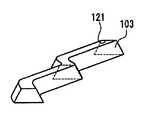
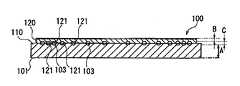
또한, 본 실시 형태의 도광판(100)은, 광원(200)으로부터 방사된 광(전자파)을 면방사로 변환하여 출광면(123)(방사면)으로부터 출광하기 위한 것이며, 도광판 본체(101)(소자 본체)가, 외부 공기층보다 굴절율(유전율)이 큰 재질로 구성된 대 략 판 모양의 형상을 이루고 있다. 또한, 이 도광판 본체(101)의 내부에는, 폐공간(103)이 복수 형성되어 있다.In addition, the
또한, 상기 도광판(100)은, 광원(200)으로부터 광이 출광되는 제1 영역 A(도광 영역)와, 상기 출광면(123)을 포함하는 제2 영역 B(출광 영역)와, 상기 제1 영역 A로부터 제 2 영역 B까지 광을 통과시키는 제3 영역 C(통과 영역)로 구분되며, 상기 폐공간(103)은 제3 영역 C에 형성되어 있다. 또한, 상기 제2 영역 B에 위치하는 출광면(123)에는 광의 전반사를 억제하기 위한 전반사 억제층(125)이 형성되어 있다.In addition, the
구체적으로 설명하면, 도광판 본체(101)는 광원(200)이 양측에 배치되는 제1 부재(110)와, 출광면(123)을 갖는 제2 부재(120)가 밀착되어 구성되어 있다. 그리고, 제2 부재(120)에는 한 면에 복수의 오목부(121)가 형성되어 있다. 또한, 이 오목부(121)가 형성된 면에서 제2 부재(120)가 제1 부재(110)에 밀착하여 접합됨으로써, 오목부(121)에 의해 폐공간(103)이 구성되어 있다. 즉, 제1 부재(110)에 의해 상기 제1 영역 A가 구성되고, 제2 부재(120)의 오목부(121)가 형성된 층에 의해 상기 제3 영역 C가 구성되고, 제2 부재(120)의 제2 영역 B보다 출광면(123) 측에 의해 상기 제2 영역 B가 구성되어 있다.Specifically, the light guide plate
또한, 상기 제1 부재(110)는 판 형상 부재로 구성되고, 예를 들면 아크릴 도광체로 구성되어 있다. 또한, 제2 부재(120)는 시트 형상 부재로 구성되고, 예를 들면 폴리카보네이트페이스의 확산 시트로 구성되어 있다. 또한, 이 제1 부재(110) 및 제2 부재(120)는, 대략 동일한 굴절율을 갖는 소재로 구성되어 있기 때문에, 제1 내지 제3의 전체 영역 A, B, C에 있어서 도광판 본체(101)는, 대략 동일한 굴절율을 갖게 된다.In addition, the said
또한, 제1 부재(110)는, 제2 부재(120)와의 접합면이 평면으로 형성되어 있으며, 이 때문에 제2 부재(120)의 오목부(121)에 의해 형성되는 복수의 폐공간(103)은, 그 저면(출광면(123)에 대해서 반대측의 면)이 서로 평행하고 또한 평면으로 형성되어 있다. 또한, 상기 제2 부재(120)는 두께가 대략 균일하게 형성되어 있기 때문에, 폐공간(103)은 그 저면이 상기 출광면(123)과 대략 평행하게 형성되어 있다.Moreover, the
또한, 복수의 폐공간(103)(오목부(121))은, 그 상면(출광면(123)측의 면)이 서로 평행하고, 또한 평면으로 형성되어 있음과 함께, 상기 출광면(123) 및 폐공간(103)의 저면에 대략 평행하게 형성되어 있다.In addition, the plurality of closed spaces 103 (the concave portion 121) have their upper surfaces (surfaces on the
또한, 이 폐공간(103)은 상면이 저면보다 좁게 형성되어 있으며, 보다 구체적으로는, 폐공간(103)은 저면이 상면보다 폭이 좁은 단면이 대략 사다리 형상으로 형성되어 있다. 또, 도시한 예에서는 폐공간(103)의 단면은, 그 기울어진 변이 서로 다른 방향으로 대략 동일한 각도로 경사진 사다리 형상으로 형성되어 있다. 또, 본 실시 형태의 폐공간(103)의 형상은, 평면에서 보았을 때 원 형상(상면 및 저면이 원형)으로 형성되어 있다(도 3참조). 또, 본원 발명에서 폐공간(103)(오목부(121))의 형상은, 다양한 형상의 것을 채용 가능하다. 또한, 본 실시 형태와 같이 폐공간(103)(오목부(121))의 단면을 사다리 형상으로 형성하는 경우라도, 다양한 형상의 것을 채용 가능하다. 즉, 도 4a에 도시한 바와 같이 평면에서 보았을 때 직선 부분과 원호 부분을 갖는 형상이나, 도 4b에 도시한 바와 같이 평면에서 보았을 때 타원 형상이나, 도 4c에 도시한 바와 같이 평면에서 보았을 때 만곡선을 갖는 형상이나, 도 4d에 도시한 바와 같이 평면에서 보았을 때 사각형상의 것을 채용할 수도 있다.In addition, the
또한, 이 폐공간(103)은, 도광판 본체(101)를 구성하는 재질보다 굴절율이 작아지도록 형성되어 있다. 구체적으로는, 상기 오목부(121)에 공기를 개재시킨 상태에서 제1 부재(110)와 제2 부재(120)를 밀착하여 폐공간(103)이 공기층이 되도록 구성시키는 것이나, 상기 오목부(121)에 도광판 본체(101)를 구성하는 재질보다 굴절율이 작은 개체층을 개재시켜, 폐공간(103)에 고체층이 충전되도록 구성할 수 있다.The
또한, 상기 오목부(121)의 형성 방법은, 예를 들면 복수의 볼록부를 갖는 금형에 의한 성형 시에 제2 부재(120)에 형성되도록 하는 방법이나, 또한 평활한 시트에 오목부를 형성하기 위한 층을 부가하는 방법이나, 또한 시트에 열이나 압력을 가함으로써 복수의 볼록부를 갖는 형의 형상을 시트에 전사하는 방법 등을 채용할 수 있다.In addition, the formation method of the said recessed
또한, 이 복수의 오목부(121)(폐공간(103))는, 평면에서 볼 때, 도 3에 도시한 바와 같이 배치되어 있으며, 광원(200)이 배치되는 측방 부근보다 중앙부 부근이, 오목부(121)의 수가 적어지도록(드문드문하게 되도록) 배치되어 있다.Moreover, these some recessed parts 121 (closed space 103) are arrange | positioned as shown in FIG. 3 in planar view, and the center part vicinity is concave rather than the side vicinity where the
또한, 상기 제2 부재(120)는 상기 접합면의 다른 면인 출광면(123)에, 상술한 전반사 억제층(125)이 형성되어 있다. 여기서, 전반사 억제층(125)은 광을 확산하는 처리가 실시된 확산층(도 2a 참조)이나, 제2 부재(120)의 표면이 거칠어진 조면화(粗面化) 처리층(도 2b 참조)으로 구성할 수 있으며, 나아가서는 제2 부재(120)의 표면에서의 전반사 억제 목적과 출광 각도 특성의 제어 목적 등의 의도를 가진 프리즘 처리층으로 구성할 수 있다. 또, 확산층을 형성하는 경우에는, 제2 부재(120)의 성형 시에 출광면 측에 확산제를 혼입하는 방법이나, 제2 부재(120)의 표면에 확산제를 접착하는 방법이 적절하게 선택 가능한 사항이다.In the
또, 도광판(100)의 저면(출광면(123)의 반대면)에, 즉 제1 부재(110)의 저면에, 광학 특성 보조 또는 추가적인 목적으로 인쇄, 요철 처리 가공, 프리즘 처리 등을 행하는 것도 적절하게 설계 변경 가능한 사항이다.Further, printing, uneven processing, prism processing, etc., may be performed on the bottom surface of the light guide plate 100 (opposite side of the light exit surface 123), that is, on the bottom surface of the
다음으로, 상기 도광판의 제조 방법에 대해서 개략적으로 설명한다.Next, the manufacturing method of the said light guide plate is outlined.
우선, 예를 들면 아크릴 도광체로 구성된 판 형상의 제1 부재(110)와, 예를 들면 폴리카보네이트페이스의 확산 시트로 구성된 시트 형상의 제2 부재(120)를 준비한다. 여기서, 제2 부재(120)의 접합면에는, 복수의 오목부(121)를 형성시켜 둔다. 이 오목부(121)는 개구측(접합면측)이 넓어지도록 형성해 둔다. 또한, 제1 부재(110)의 접합면은 평면이 되도록 형성해 둔다.First, for example, a plate-shaped
상기 준비된 제1 부재(110)의 접합면에, 제2 부재(120)의 오목부(121)가 형성된 면을 접착한다. 여기서 접착 시에는, 예를 들면 자외선 경화성 수지를 접착제로서 이용하고, 이에 자외선을 조사하여 양자를 접합하는 방법을 채용할 수 있다.The surface on which the recessed
또, 이 접착 시에, 미리 상기 제2 부재(120)의 오목부(121)에 제1 부재(110) 및 제2 부재(120)보다 굴절율이 높은 고체층을 형성해 둘 수도 있다.In this bonding, a solid layer having a higher refractive index than the
상기 구성으로 이루어지는 도광판(100)을 갖는 액정 표시 장치에 있어서는, 광원(200)으로부터의 광이 도광판(100)을 통과하고 도광판(100)의 출광면(123)으로부터 액정 표시 패널(300)을 향하여 방사된다.In the liquid crystal display device having the
이 광의 도광판(100)의 통과 시에는, 광원(200)으로부터의 광은, 도광판(100)의 제1 영역 A(제1 부재(110))로부터 제3 영역 C(제2 부재(120)의 하층)을 통과하여 제2 영역 B의 출광면(123)으로부터 출광된다. 이와 같이 도광판(100) 내에서 광은, 제3 영역 C에 있어서 폐공간(103) 이외의 부분을 제2 영역 B측으로 통과하기 때문에 종래 기술과 같이 점접 부분을 통과하는 것에 비하여, 광이 출광면(123)측으로 적확하게 통과하여 광로를 짧게 할 수 있어, 광원(200)으로부터의 광을 효율적으로 방사할 수 있다. 또한, 점 접촉하는 종래의 것에 비하여 제1 부재(110)와 제2 부재(120)와의 접합 면적이 넓어지므로, 양자의 접착력이 강하고, 기계적 강도가 높아지는 등의 이점을 갖는다. 또한, 오목부(121)에 고체층을 형성함으로써, 기계적 강도가 보다 높아지는 등의 이점을 갖는다.When the light passes through the
또한, 제2 영역 B(제2 부재(120))의 출광면(123)에는 전반사 억제층(125)이 형성되어 있기 때문에, 출광면(123)에까지 도달한 광이 전반사 억제층(125)에서 산란되고, 전반사각을 벗어나지 않은 광이라도 출광면(123)으로부터 출광되어, 광원(200)으로부터의 광의 이용 효율의 향상을 도모할 수 있다.In addition, since the total
또한, 복수의 오목부(121)(폐공간(103))는 광원(200)으로부터 가까운 측방 부근보다 중앙 부분에 있어서 수가 적어지도록 배치되어 있기 때문에, 측방 부근의 광에 비하여 중앙 부근의 광이 제2 영역 B측으로 통과하기 쉬워, 이 때문에 출광면(123)으로부터 균일한 면 방사가 가능하게 된다.In addition, since the plurality of recesses 121 (closed space 103) are arranged so that the number of the recesses 121 (closed space 103) is smaller in the center portion than in the vicinity of the side near the
또한, 제1 영역 A를 통과하는 광 중 일부는, 폐공간(103)의 바닥부에서 하방으로 반사되지만, 이 폐공간(103)의 바닥부는 평면에 형성되어 있기 때문에, 난반사를 일으키지 않아, 광의 제어가 용이하다. 또한, 복수의 폐공간(103)의 바닥부는 서로 평행하고 또한 평면으로 형성되어 있기 때문에, 그 제어는 더욱 용이하다는 이점을 갖는다.In addition, some of the light passing through the first region A is reflected downward from the bottom of the
또한, 제2 영역 B의 출광면(123)에서 일부의 광이 반사되고, 이 반사광이 폐공간(103)의 상면에 있어서 반사되지만, 이 폐공간(103)의 상면은 평면에 형성되어 있기 때문에, 난반사를 일으키지 않아, 광의 제어가 용이하다. 또한, 복수의 폐공간(103)의 상면은, 서로 평행하고 또한 평면으로 형성되어 있기 때문에, 그 제어는 더욱 용이하다는 이점을 갖는다.In addition, a part of light is reflected on the
또, 본 실시 형태는 상기 구성을 채용하였기 때문에, 상기 이점을 갖는 것이었지만, 본원 발명은 상기 실시 형태의 구성에 한정되는 것이 아니라, 본원 발명이 의도하는 범위 내에서 적절하게 설계 변경 가능하다.Moreover, since this embodiment employ | adopts the said structure, it has the said advantage, but this invention is not limited to the structure of the said embodiment, Design can be changed suitably within the range which this invention intends.
즉, 상기 실시 형태에서는, 전자파의 일례로서 광을 예로 들어 설명하였지만, 그 밖의 X선 등을 면방사하기 위해서 이용할 수도 있다.That is, in the above embodiment, although light has been described as an example of electromagnetic waves, it can be used for surface radiation of other X-rays and the like.
또한, 전자파 전반에 걸쳐 실시되는 본원 발명은, 면방사 변환 소자를 구성하는 부재의 상(相)이 결정 또는 비결정체 등, 상태가 고체 또는 액체 등에 한정되지 않고, 적절하게 설계 변경 가능하다.In addition, according to the present invention carried out throughout the electromagnetic wave, the phase of the members constituting the surface radiating conversion element is not limited to solid or liquid, such as crystals or amorphous bodies, and can be appropriately changed in design.
또한, 상기 실시 형태와 같이 액정 표시 장치에 이용하는 경우에도, 예를 들면 도 5에 도시한 바와 같이, 소위 프론트라이트식의 액정 표시 장치에도 이용 가능하다. 도 5에 도시한 액정 표시 장치는, 도광판(100)의 양측에 광원(200)이 배치되고, 도광판(100)의 하면에 반사 모드를 갖는 액정 표시 패널(300)이 장치되어 있다. 즉, 도광판의 출광면(123)이 저면측에 형성되어 있으며, 도시한 예는, 상기 실시 형태의 설명에서의 상면측이 저면측, 저면측이 상면측으로 되어 있는 것이다. 또, 도 5에 도시한 도광판(100)의 상면(출광면(123)의 반대면)에 요철 처리 가공, 조면화 처리, 프리즘 처리 등을 행할 수도 있다.Moreover, also when using for a liquid crystal display device like the said embodiment, as shown, for example in FIG. 5, it can use also for a so-called front-light liquid crystal display device. In the liquid crystal display shown in FIG. 5, the
또한, 상기 실시 형태에는 도광판(100)의 양측에 광원(200)이 배치된 것에 대해서 설명하였지만, 예를 들면 도 6이나 도 7에 도시한 바와 같이, 도광판(100)의 일측에만 광원(200)을 배치하는 것도 본원 발명이 의도하는 범위 내이다. 또, 도 6에 도시한 것은 소위 백라이트식의 액정 표시 장치이고, 도 7에 도시한 것은 소위 프론트라이트식의 액정 표시 장치이다. 이 도 6 및 도 7에 도시한 도광판(100)은, 광원(200)이 배치되는 일측으로부터 반대측에 걸쳐 두께가 얇아지는, 소위 쐐기형을 이루고 있으며, 구체적으로는 출광면(123)에 대해서 그 반대면(도 6의 저면, 도 7의 상면)이 기울어져 형성되어 있다. 또, 도 6 및 도 7에 도시한 도광판(100)의 폐공간(103)은 출광면(123)측의 면(도 6의 상면, 도 7의 저면) 및 출광면(123)에 대한 반대면(도 6의 저면, 도 7의 상면)이 출광면(123)에 평행하게 되도록 형성되어 있다. 또한, 복수의 폐공간(103)은 광원(200)이 배치되는 일측으로부터 반대측에 걸쳐 수가 적어지도록 배치되어 있다.In addition, although the
또한, 상기 실시 형태와 같이 액정 표시 장치에 이용하는 경우에도, 예를 들면 도 8에 도시한 바와 같이, 소위 직하식(直下式)의 액정 표시 장치에도 이용 가능하다. 이 경우, 복수의 폐공간(103)에 의해, 광원으로부터의 광을 효율적으로 지향성을 변경할 수 있으며, 표시 장치로서 적확한 지향성으로 용이하게 제어할 수 있다. 또한, 이 경우에는, 복수의 폐공간(103)을, 평면에서 보았을 때(도 3에 도시한 바와 같이 보았을 때에) 면내 분포 상태를 조정하여 배치함으로써, 적확한 광량 분포를 만들어낼 수 있다.Moreover, also when using for a liquid crystal display device like the said embodiment, as shown, for example in FIG. 8, it can also be used for what is called a direct type liquid crystal display device. In this case, the plurality of
또한, 상기 실시 형태에서는, 제2 부재(200)에 형성된 오목부(121)에 의해 폐공간(103)이 형성되는 것에 대해서 설명하였지만, 본원 발명은 이에 한정되는 것은 아니다. 예를 들면, 상기 실시 형태와 같은 제1 부재(110)에 폐공간을 형성하기 위한 오목부를 형성하거나, 또한 제1 부재와 제2 부재와의 사이에 뚫린 구멍을 갖는 제3 부재를 개재시켜서 뚫린 구멍으로부터 폐공간을 형성하는 것도 본원 발명이 의도하는 범위 내이다. 또한, 도 9 또는 도 10에 도시한 바와 같이, 제1 부재(110) 및 제2 부재(120)의 쌍방에 폐공간(103)을 형성하기 위한 오목부(121)를 형성하는 것도 본원 발명이 의도하는 범위 내이다. 또, 이와 같이 제1 부재(110) 및 제2 부재(120)의 쌍방에 오목부(121)를 형성함에 있어서, 도 9에 도시한 바와 같이 제1 부재(110)의 복수의 오목부(121)가 제2 부재(120)의 복수의 오목부(121)와 대응하는 위치에 형성되고, 제1 부재(110)의 하나의 오목부(121)와 제2 부재(120)의 하나의 오목부(121)에 의해 하나의 폐공간(103)이 형성되도록 할 수도 있다. 또한, 제1 부재(110) 및 제2 부재(120)의 쌍방에 오목부(121)를 형성함에 있어서, 도 10에 도시한 바와 같이 제1 부재(110)의 복수의 오목부(121)를 제2 부재(120)의 복수의 오목부(121)와 대응하는 위치에 형성하지 않고, 제1 부재(110)의 복수의 오목부(121) 중, 제2 부재(120)의 표면과에 의해 폐공간(103)을 형성하는 오목부(121)가 존재하거나, 또한 제2 부재(121)의 복수의 오목부(121) 중, 제1 부재(110)의 이면과에 의해 폐공간(103)을 형성하는 오목부(121)가 존재하도록 설계 변경할 수도 있다.In addition, although the said embodiment demonstrated that the
본 발명에 따르면, 방사원으로부터 방사되는 전자파를 효율적으로 방사면으로부터 방사할 수 있다.According to the present invention, electromagnetic waves emitted from a radiation source can be efficiently emitted from the radiation plane.
Claims (43)
Translated fromKoreanApplications Claiming Priority (2)
| Application Number | Priority Date | Filing Date | Title |
|---|---|---|---|
| JPJP-P-2003-00053551 | 2003-02-28 | ||
| JP2003053551 | 2003-02-28 |
Publications (2)
| Publication Number | Publication Date |
|---|---|
| KR20040077572A KR20040077572A (en) | 2004-09-04 |
| KR100799786B1true KR100799786B1 (en) | 2008-01-31 |
Family
ID=33398250
Family Applications (1)
| Application Number | Title | Priority Date | Filing Date |
|---|---|---|---|
| KR1020040013744AExpired - Fee RelatedKR100799786B1 (en) | 2003-02-28 | 2004-02-28 | Method of manufacturing surface emission conversion element, liquid crystal display device and surface emission conversion element |
Country Status (4)
| Country | Link |
|---|---|
| US (1) | US7537369B2 (en) |
| KR (1) | KR100799786B1 (en) |
| CN (2) | CN101441292A (en) |
| TW (1) | TWI352228B (en) |
Families Citing this family (52)
| Publication number | Priority date | Publication date | Assignee | Title |
|---|---|---|---|---|
| TWI289708B (en) | 2002-12-25 | 2007-11-11 | Qualcomm Mems Technologies Inc | Optical interference type color display |
| US7342705B2 (en) | 2004-02-03 | 2008-03-11 | Idc, Llc | Spatial light modulator with integrated optical compensation structure |
| US7706050B2 (en) | 2004-03-05 | 2010-04-27 | Qualcomm Mems Technologies, Inc. | Integrated modulator illumination |
| US7750886B2 (en) | 2004-09-27 | 2010-07-06 | Qualcomm Mems Technologies, Inc. | Methods and devices for lighting displays |
| US7813026B2 (en) | 2004-09-27 | 2010-10-12 | Qualcomm Mems Technologies, Inc. | System and method of reducing color shift in a display |
| US20070058391A1 (en)* | 2005-09-14 | 2007-03-15 | Wilson Randall H | Light extraction layer |
| US7603001B2 (en) | 2006-02-17 | 2009-10-13 | Qualcomm Mems Technologies, Inc. | Method and apparatus for providing back-lighting in an interferometric modulator display device |
| US20070203267A1 (en)* | 2006-02-28 | 2007-08-30 | 3M Innovative Properties Company | Optical display with fluted optical plate |
| US7766531B2 (en)* | 2006-03-29 | 2010-08-03 | 3M Innovative Properties Company | Edge-lit optical display with fluted optical plate |
| US7766498B2 (en) | 2006-06-21 | 2010-08-03 | Qualcomm Mems Technologies, Inc. | Linear solid state illuminator |
| US7845841B2 (en) | 2006-08-28 | 2010-12-07 | Qualcomm Mems Technologies, Inc. | Angle sweeping holographic illuminator |
| US8107155B2 (en) | 2006-10-06 | 2012-01-31 | Qualcomm Mems Technologies, Inc. | System and method for reducing visual artifacts in displays |
| EP1943555B1 (en) | 2006-10-06 | 2012-05-02 | QUALCOMM MEMS Technologies, Inc. | Optical loss structure integrated in an illumination apparatus of a display |
| US7855827B2 (en) | 2006-10-06 | 2010-12-21 | Qualcomm Mems Technologies, Inc. | Internal optical isolation structure for integrated front or back lighting |
| US7864395B2 (en) | 2006-10-27 | 2011-01-04 | Qualcomm Mems Technologies, Inc. | Light guide including optical scattering elements and a method of manufacture |
| US7777954B2 (en) | 2007-01-30 | 2010-08-17 | Qualcomm Mems Technologies, Inc. | Systems and methods of providing a light guiding layer |
| US7733439B2 (en)* | 2007-04-30 | 2010-06-08 | Qualcomm Mems Technologies, Inc. | Dual film light guide for illuminating displays |
| CN100498390C (en)* | 2007-07-20 | 2009-06-10 | 友达光电股份有限公司 | light guide plate |
| WO2009032813A2 (en) | 2007-09-06 | 2009-03-12 | 3M Innovative Properties Company | Lightguides having light extraction structures providing regional control of light output |
| ATE534500T1 (en)* | 2007-09-06 | 2011-12-15 | 3M Innovative Properties Co | METHOD FOR SHAPING MOLDING TOOLS AND METHOD FOR SHAPING ARTICLES USING THE MOLDING TOOLS |
| EP2205521A4 (en)* | 2007-09-06 | 2013-09-11 | 3M Innovative Properties Co | Tool for making microstructured articles |
| CN101821659B (en) | 2007-10-11 | 2014-09-24 | 3M创新有限公司 | Chromatic confocal sensor |
| CN101821302A (en)* | 2007-10-11 | 2010-09-01 | 3M创新有限公司 | Highly functional multiphoton curable reactive substance |
| KR101454171B1 (en)* | 2007-11-28 | 2014-10-27 | 삼성전자주식회사 | Reflective display device and manufacturing method of light guide plate |
| EP2232531B1 (en)* | 2007-12-12 | 2018-09-19 | 3M Innovative Properties Company | Method for making structures with improved edge definition |
| JP2011512006A (en) | 2008-01-30 | 2011-04-14 | デジタル オプティクス インターナショナル,リミティド ライアビリティ カンパニー | Thin lighting system |
| US8721149B2 (en) | 2008-01-30 | 2014-05-13 | Qualcomm Mems Technologies, Inc. | Illumination device having a tapered light guide |
| US8654061B2 (en) | 2008-02-12 | 2014-02-18 | Qualcomm Mems Technologies, Inc. | Integrated front light solution |
| WO2009102731A2 (en) | 2008-02-12 | 2009-08-20 | Qualcomm Mems Technologies, Inc. | Devices and methods for enhancing brightness of displays using angle conversion layers |
| KR20100124754A (en)* | 2008-02-22 | 2010-11-29 | 오스람 옵토 세미컨덕터스 게엠베하 | Optical arrangement and production method |
| JP5801558B2 (en)* | 2008-02-26 | 2015-10-28 | スリーエム イノベイティブ プロパティズ カンパニー | Multi-photon exposure system |
| CN101533120B (en)* | 2008-03-14 | 2011-07-27 | 旭丽电子(广州)有限公司 | Display device |
| WO2009129264A1 (en) | 2008-04-15 | 2009-10-22 | Qualcomm Mems Technologies, Inc. | Light with bi-directional propagation |
| US7639918B2 (en)* | 2008-05-05 | 2009-12-29 | Visteon Global Technologies, Inc. | Manifold-type lightguide with reduced thickness |
| CN102047155B (en) | 2008-05-28 | 2013-04-03 | 高通Mems科技公司 | Light guide panel with light turning microstructure, its manufacturing method and display device |
| KR20100009078A (en)* | 2008-07-17 | 2010-01-27 | 삼성광주전자 주식회사 | A display and refrigerator with the same |
| US8358266B2 (en) | 2008-09-02 | 2013-01-22 | Qualcomm Mems Technologies, Inc. | Light turning device with prismatic light turning features |
| JP5492899B2 (en) | 2008-10-10 | 2014-05-14 | クォルコム・メムズ・テクノロジーズ・インコーポレーテッド | Distributed lighting system |
| KR20110104090A (en) | 2009-01-13 | 2011-09-21 | 퀄컴 엠이엠스 테크놀로지스, 인크. | Large Area Light Panels and Screens |
| JP5369840B2 (en)* | 2009-04-01 | 2013-12-18 | ソニー株式会社 | Method for manufacturing light guide plate |
| TWI407162B (en)* | 2009-04-30 | 2013-09-01 | Coretronic Corp | Light guide plate and backlight module |
| CN102449512A (en) | 2009-05-29 | 2012-05-09 | 高通Mems科技公司 | Illumination devices and methods of fabrication thereof |
| US8402647B2 (en) | 2010-08-25 | 2013-03-26 | Qualcomm Mems Technologies Inc. | Methods of manufacturing illumination systems |
| US8902484B2 (en) | 2010-12-15 | 2014-12-02 | Qualcomm Mems Technologies, Inc. | Holographic brightness enhancement film |
| US8971680B2 (en)* | 2012-05-22 | 2015-03-03 | Sharp Laboratories Of America, Inc. | Waveguide with Controlled Light Collimation |
| CN104375236B (en)* | 2014-11-26 | 2017-10-24 | 深圳市华星光电技术有限公司 | Light guide plate, backlight module and display |
| JP6457872B2 (en) | 2015-04-10 | 2019-01-23 | 株式会社ジャパンディスプレイ | Display device, lighting device, light guide plate, and manufacturing method thereof |
| KR102671558B1 (en)* | 2016-07-06 | 2024-06-04 | 삼성디스플레이 주식회사 | Backlight unit, display device including the same, and fabrication method thereof |
| KR20180026611A (en)* | 2016-09-02 | 2018-03-13 | 삼성디스플레이 주식회사 | Display apparatus and fabrication method thereof |
| KR102651691B1 (en) | 2017-11-01 | 2024-03-27 | 닛토덴코 가부시키가이샤 | Light distribution structures and elements, related methods and uses |
| CN110320587B (en)* | 2018-03-30 | 2021-02-26 | 光宝电子(广州)有限公司 | Light guide plate and light source module |
| CN111239887B (en)* | 2020-03-24 | 2024-06-14 | 杭州矽能新材料有限公司 | Light guide film, production method thereof and light guide device |
Citations (7)
| Publication number | Priority date | Publication date | Assignee | Title |
|---|---|---|---|---|
| KR20010003887A (en)* | 1999-06-25 | 2001-01-15 | 김우연 | Light guide panel of flat panel display and method for fabricating the same |
| JP2001091709A (en)* | 1999-09-24 | 2001-04-06 | Keiwa Inc | Optical sheet, optical unit and backlight unit |
| JP2001215312A (en)* | 2000-02-02 | 2001-08-10 | Nitto Denko Corp | Optical film |
| US20010053074A1 (en)* | 2000-04-27 | 2001-12-20 | Kuraray Co., Ltd. | Planar light source and display device using the same |
| WO2002025167A1 (en)* | 2000-09-25 | 2002-03-28 | Mitsubishi Rayon Co., Ltd. | Light source device |
| JP2002311214A (en)* | 2001-04-10 | 2002-10-23 | Tomoegawa Paper Co Ltd | Optical film and manufacturing method thereof |
| JP2002350615A (en)* | 2001-05-23 | 2002-12-04 | Enplas Corp | Assembly of diffusing member, surface light source device and image display device |
Family Cites Families (10)
| Publication number | Priority date | Publication date | Assignee | Title |
|---|---|---|---|---|
| JP3325710B2 (en)* | 1994-07-27 | 2002-09-17 | 日本ライツ株式会社 | Method for manufacturing light guide plate and mold for molding the same, and surface light source device |
| JPH0996814A (en) | 1995-09-29 | 1997-04-08 | Toshiba Lighting & Technol Corp | Lighting equipment, backlight and liquid crystal display |
| US5961198A (en)* | 1996-02-02 | 1999-10-05 | Hitachi, Ltd. | Liquid crystal display device and method of manufacturing backlighting light guide panel therefor |
| US6334689B1 (en)* | 1997-01-30 | 2002-01-01 | Hitachi, Ltd. | Liquid crystal display |
| JP3905661B2 (en) | 1999-02-25 | 2007-04-18 | 株式会社クラレ | Method for manufacturing surface light source element |
| TW586023B (en)* | 1999-09-24 | 2004-05-01 | Keiwa Inc | Optical sheet |
| JP2001264698A (en)* | 2000-03-23 | 2001-09-26 | Mitsubishi Electric Corp | Lighting device and lighting method |
| JP2001338507A (en) | 2000-05-29 | 2001-12-07 | Kuraray Co Ltd | Surface light source element and display device using the same |
| JP4472221B2 (en) | 2000-09-25 | 2010-06-02 | 三菱レイヨン株式会社 | Light source device having light leakage modulator |
| KR100765138B1 (en)* | 2001-04-09 | 2007-10-15 | 삼성전자주식회사 | Backlight Assembly and Liquid Crystal Display Using Same |
- 2004
- 2004-02-27CNCNA2008101454504Apatent/CN101441292A/enactivePending
- 2004-02-27CNCNB200410008246XApatent/CN100454087C/ennot_activeExpired - Fee Related
- 2004-02-27USUS10/787,188patent/US7537369B2/ennot_activeExpired - Fee Related
- 2004-02-27TWTW093105151Apatent/TWI352228B/ennot_activeIP Right Cessation
- 2004-02-28KRKR1020040013744Apatent/KR100799786B1/ennot_activeExpired - Fee Related
Patent Citations (7)
| Publication number | Priority date | Publication date | Assignee | Title |
|---|---|---|---|---|
| KR20010003887A (en)* | 1999-06-25 | 2001-01-15 | 김우연 | Light guide panel of flat panel display and method for fabricating the same |
| JP2001091709A (en)* | 1999-09-24 | 2001-04-06 | Keiwa Inc | Optical sheet, optical unit and backlight unit |
| JP2001215312A (en)* | 2000-02-02 | 2001-08-10 | Nitto Denko Corp | Optical film |
| US20010053074A1 (en)* | 2000-04-27 | 2001-12-20 | Kuraray Co., Ltd. | Planar light source and display device using the same |
| WO2002025167A1 (en)* | 2000-09-25 | 2002-03-28 | Mitsubishi Rayon Co., Ltd. | Light source device |
| JP2002311214A (en)* | 2001-04-10 | 2002-10-23 | Tomoegawa Paper Co Ltd | Optical film and manufacturing method thereof |
| JP2002350615A (en)* | 2001-05-23 | 2002-12-04 | Enplas Corp | Assembly of diffusing member, surface light source device and image display device |
Also Published As
| Publication number | Publication date |
|---|---|
| KR20040077572A (en) | 2004-09-04 |
| TWI352228B (en) | 2011-11-11 |
| CN101441292A (en) | 2009-05-27 |
| US7537369B2 (en) | 2009-05-26 |
| CN1530702A (en) | 2004-09-22 |
| TW200502630A (en) | 2005-01-16 |
| CN100454087C (en) | 2009-01-21 |
| US20040228112A1 (en) | 2004-11-18 |
Similar Documents
| Publication | Publication Date | Title |
|---|---|---|
| KR100799786B1 (en) | Method of manufacturing surface emission conversion element, liquid crystal display device and surface emission conversion element | |
| US8427603B2 (en) | Area light source device and liquid crystal display device | |
| US9606288B2 (en) | Slim waveguide coupling apparatus and method | |
| CN102844608B (en) | Backlight device and liquid crystal display device | |
| US7206491B2 (en) | Light guide device and backlight module using the same | |
| JP5193987B2 (en) | Light guide plate and backlight module | |
| JP5602713B2 (en) | Light guide module, backlight module, and light guide module manufacturing method | |
| US10761259B2 (en) | Light guide assembly, light collimation assembly, backlight module and display device | |
| CN104620041B (en) | Planar light source device and use the display device of this planar light source device | |
| JP2009289701A (en) | Lighting device, plane light source device, and liquid crystal display | |
| JP2009224316A (en) | Illuminating device and liquid crystal display device | |
| WO2011065053A1 (en) | Light guide plate, light guide unit, lighting device, and display device | |
| EP2578931A1 (en) | Surface-emitting led cover, lighting device and display device | |
| JP5617212B2 (en) | Light guide plate, light guide plate manufacturing method and backlight unit | |
| JP2006189796A (en) | Light guide plate and backlight module | |
| JP4267485B2 (en) | Surface radiation conversion element, liquid crystal display device, and method of manufacturing surface radiation conversion element | |
| JP2020119711A (en) | Surface light source device and display device | |
| JP2005135815A (en) | Surface light source device and display device using the surface light source device | |
| JP2008027649A (en) | Light source device and backlight device | |
| CN115113321A (en) | lighting device | |
| JP5950529B2 (en) | Surface light source device and display device including the same | |
| JP2012209088A (en) | Backlight device | |
| CN100395620C (en) | Light guide plate and backlight module using the light guide plate | |
| JP4473035B2 (en) | Illumination device and display device including the same | |
| JP2012209086A (en) | Backlight device and light guide plate |
Legal Events
| Date | Code | Title | Description |
|---|---|---|---|
| A201 | Request for examination | ||
| PA0109 | Patent application | St.27 status event code:A-0-1-A10-A12-nap-PA0109 | |
| PA0201 | Request for examination | St.27 status event code:A-1-2-D10-D11-exm-PA0201 | |
| PG1501 | Laying open of application | St.27 status event code:A-1-1-Q10-Q12-nap-PG1501 | |
| D13-X000 | Search requested | St.27 status event code:A-1-2-D10-D13-srh-X000 | |
| D14-X000 | Search report completed | St.27 status event code:A-1-2-D10-D14-srh-X000 | |
| E902 | Notification of reason for refusal | ||
| PE0902 | Notice of grounds for rejection | St.27 status event code:A-1-2-D10-D21-exm-PE0902 | |
| T11-X000 | Administrative time limit extension requested | St.27 status event code:U-3-3-T10-T11-oth-X000 | |
| PN2301 | Change of applicant | St.27 status event code:A-3-3-R10-R13-asn-PN2301 St.27 status event code:A-3-3-R10-R11-asn-PN2301 | |
| T11-X000 | Administrative time limit extension requested | St.27 status event code:U-3-3-T10-T11-oth-X000 | |
| T11-X000 | Administrative time limit extension requested | St.27 status event code:U-3-3-T10-T11-oth-X000 | |
| T11-X000 | Administrative time limit extension requested | St.27 status event code:U-3-3-T10-T11-oth-X000 | |
| T11-X000 | Administrative time limit extension requested | St.27 status event code:U-3-3-T10-T11-oth-X000 | |
| T11-X000 | Administrative time limit extension requested | St.27 status event code:U-3-3-T10-T11-oth-X000 | |
| T11-X000 | Administrative time limit extension requested | St.27 status event code:U-3-3-T10-T11-oth-X000 | |
| T11-X000 | Administrative time limit extension requested | St.27 status event code:U-3-3-T10-T11-oth-X000 | |
| T11-X000 | Administrative time limit extension requested | St.27 status event code:U-3-3-T10-T11-oth-X000 | |
| T11-X000 | Administrative time limit extension requested | St.27 status event code:U-3-3-T10-T11-oth-X000 | |
| T11-X000 | Administrative time limit extension requested | St.27 status event code:U-3-3-T10-T11-oth-X000 | |
| T11-X000 | Administrative time limit extension requested | St.27 status event code:U-3-3-T10-T11-oth-X000 | |
| T11-X000 | Administrative time limit extension requested | St.27 status event code:U-3-3-T10-T11-oth-X000 | |
| T11-X000 | Administrative time limit extension requested | St.27 status event code:U-3-3-T10-T11-oth-X000 | |
| T11-X000 | Administrative time limit extension requested | St.27 status event code:U-3-3-T10-T11-oth-X000 | |
| E13-X000 | Pre-grant limitation requested | St.27 status event code:A-2-3-E10-E13-lim-X000 | |
| P11-X000 | Amendment of application requested | St.27 status event code:A-2-2-P10-P11-nap-X000 | |
| P13-X000 | Application amended | St.27 status event code:A-2-2-P10-P13-nap-X000 | |
| E902 | Notification of reason for refusal | ||
| PE0902 | Notice of grounds for rejection | St.27 status event code:A-1-2-D10-D21-exm-PE0902 | |
| E13-X000 | Pre-grant limitation requested | St.27 status event code:A-2-3-E10-E13-lim-X000 | |
| P11-X000 | Amendment of application requested | St.27 status event code:A-2-2-P10-P11-nap-X000 | |
| P13-X000 | Application amended | St.27 status event code:A-2-2-P10-P13-nap-X000 | |
| E701 | Decision to grant or registration of patent right | ||
| PE0701 | Decision of registration | St.27 status event code:A-1-2-D10-D22-exm-PE0701 | |
| GRNT | Written decision to grant | ||
| PR0701 | Registration of establishment | St.27 status event code:A-2-4-F10-F11-exm-PR0701 | |
| PR1002 | Payment of registration fee | St.27 status event code:A-2-2-U10-U11-oth-PR1002 Fee payment year number:1 | |
| PG1601 | Publication of registration | St.27 status event code:A-4-4-Q10-Q13-nap-PG1601 | |
| R17-X000 | Change to representative recorded | St.27 status event code:A-5-5-R10-R17-oth-X000 | |
| PR1001 | Payment of annual fee | St.27 status event code:A-4-4-U10-U11-oth-PR1001 Fee payment year number:4 | |
| FPAY | Annual fee payment | Payment date:20120105 Year of fee payment:5 | |
| PR1001 | Payment of annual fee | St.27 status event code:A-4-4-U10-U11-oth-PR1001 Fee payment year number:5 | |
| LAPS | Lapse due to unpaid annual fee | ||
| PC1903 | Unpaid annual fee | St.27 status event code:A-4-4-U10-U13-oth-PC1903 Not in force date:20130125 Payment event data comment text:Termination Category : DEFAULT_OF_REGISTRATION_FEE | |
| PC1903 | Unpaid annual fee | St.27 status event code:N-4-6-H10-H13-oth-PC1903 Ip right cessation event data comment text:Termination Category : DEFAULT_OF_REGISTRATION_FEE Not in force date:20130125 | |
| R18-X000 | Changes to party contact information recorded | St.27 status event code:A-5-5-R10-R18-oth-X000 |