KR100799735B1 - Metal oxide formation method and apparatus for performing the same - Google Patents
Metal oxide formation method and apparatus for performing the sameDownload PDFInfo
- Publication number
- KR100799735B1 KR100799735B1KR1020060064250AKR20060064250AKR100799735B1KR 100799735 B1KR100799735 B1KR 100799735B1KR 1020060064250 AKR1020060064250 AKR 1020060064250AKR 20060064250 AKR20060064250 AKR 20060064250AKR 100799735 B1KR100799735 B1KR 100799735B1
- Authority
- KR
- South Korea
- Prior art keywords
- gas
- substrate
- metal precursor
- oxidizing gas
- precursor film
- Prior art date
- Legal status (The legal status is an assumption and is not a legal conclusion. Google has not performed a legal analysis and makes no representation as to the accuracy of the status listed.)
- Active
Links
Images


Classifications
- C—CHEMISTRY; METALLURGY
- C01—INORGANIC CHEMISTRY
- C01G—COMPOUNDS CONTAINING METALS NOT COVERED BY SUBCLASSES C01D OR C01F
- C01G25/00—Compounds of zirconium
- C01G25/02—Oxides
- C—CHEMISTRY; METALLURGY
- C23—COATING METALLIC MATERIAL; COATING MATERIAL WITH METALLIC MATERIAL; CHEMICAL SURFACE TREATMENT; DIFFUSION TREATMENT OF METALLIC MATERIAL; COATING BY VACUUM EVAPORATION, BY SPUTTERING, BY ION IMPLANTATION OR BY CHEMICAL VAPOUR DEPOSITION, IN GENERAL; INHIBITING CORROSION OF METALLIC MATERIAL OR INCRUSTATION IN GENERAL
- C23C—COATING METALLIC MATERIAL; COATING MATERIAL WITH METALLIC MATERIAL; SURFACE TREATMENT OF METALLIC MATERIAL BY DIFFUSION INTO THE SURFACE, BY CHEMICAL CONVERSION OR SUBSTITUTION; COATING BY VACUUM EVAPORATION, BY SPUTTERING, BY ION IMPLANTATION OR BY CHEMICAL VAPOUR DEPOSITION, IN GENERAL
- C23C16/00—Chemical coating by decomposition of gaseous compounds, without leaving reaction products of surface material in the coating, i.e. chemical vapour deposition [CVD] processes
- C23C16/44—Chemical coating by decomposition of gaseous compounds, without leaving reaction products of surface material in the coating, i.e. chemical vapour deposition [CVD] processes characterised by the method of coating
- C23C16/455—Chemical coating by decomposition of gaseous compounds, without leaving reaction products of surface material in the coating, i.e. chemical vapour deposition [CVD] processes characterised by the method of coating characterised by the method used for introducing gases into reaction chamber or for modifying gas flows in reaction chamber
- C23C16/45523—Pulsed gas flow or change of composition over time
- C23C16/45525—Atomic layer deposition [ALD]
- C—CHEMISTRY; METALLURGY
- C01—INORGANIC CHEMISTRY
- C01G—COMPOUNDS CONTAINING METALS NOT COVERED BY SUBCLASSES C01D OR C01F
- C01G23/00—Compounds of titanium
- C01G23/04—Oxides; Hydroxides
- C01G23/047—Titanium dioxide
- C—CHEMISTRY; METALLURGY
- C01—INORGANIC CHEMISTRY
- C01G—COMPOUNDS CONTAINING METALS NOT COVERED BY SUBCLASSES C01D OR C01F
- C01G27/00—Compounds of hafnium
- C01G27/02—Oxides
- C—CHEMISTRY; METALLURGY
- C01—INORGANIC CHEMISTRY
- C01G—COMPOUNDS CONTAINING METALS NOT COVERED BY SUBCLASSES C01D OR C01F
- C01G35/00—Compounds of tantalum
- C—CHEMISTRY; METALLURGY
- C23—COATING METALLIC MATERIAL; COATING MATERIAL WITH METALLIC MATERIAL; CHEMICAL SURFACE TREATMENT; DIFFUSION TREATMENT OF METALLIC MATERIAL; COATING BY VACUUM EVAPORATION, BY SPUTTERING, BY ION IMPLANTATION OR BY CHEMICAL VAPOUR DEPOSITION, IN GENERAL; INHIBITING CORROSION OF METALLIC MATERIAL OR INCRUSTATION IN GENERAL
- C23C—COATING METALLIC MATERIAL; COATING MATERIAL WITH METALLIC MATERIAL; SURFACE TREATMENT OF METALLIC MATERIAL BY DIFFUSION INTO THE SURFACE, BY CHEMICAL CONVERSION OR SUBSTITUTION; COATING BY VACUUM EVAPORATION, BY SPUTTERING, BY ION IMPLANTATION OR BY CHEMICAL VAPOUR DEPOSITION, IN GENERAL
- C23C16/00—Chemical coating by decomposition of gaseous compounds, without leaving reaction products of surface material in the coating, i.e. chemical vapour deposition [CVD] processes
- C23C16/22—Chemical coating by decomposition of gaseous compounds, without leaving reaction products of surface material in the coating, i.e. chemical vapour deposition [CVD] processes characterised by the deposition of inorganic material, other than metallic material
- C23C16/30—Deposition of compounds, mixtures or solid solutions, e.g. borides, carbides, nitrides
- C23C16/40—Oxides
- C—CHEMISTRY; METALLURGY
- C23—COATING METALLIC MATERIAL; COATING MATERIAL WITH METALLIC MATERIAL; CHEMICAL SURFACE TREATMENT; DIFFUSION TREATMENT OF METALLIC MATERIAL; COATING BY VACUUM EVAPORATION, BY SPUTTERING, BY ION IMPLANTATION OR BY CHEMICAL VAPOUR DEPOSITION, IN GENERAL; INHIBITING CORROSION OF METALLIC MATERIAL OR INCRUSTATION IN GENERAL
- C23C—COATING METALLIC MATERIAL; COATING MATERIAL WITH METALLIC MATERIAL; SURFACE TREATMENT OF METALLIC MATERIAL BY DIFFUSION INTO THE SURFACE, BY CHEMICAL CONVERSION OR SUBSTITUTION; COATING BY VACUUM EVAPORATION, BY SPUTTERING, BY ION IMPLANTATION OR BY CHEMICAL VAPOUR DEPOSITION, IN GENERAL
- C23C16/00—Chemical coating by decomposition of gaseous compounds, without leaving reaction products of surface material in the coating, i.e. chemical vapour deposition [CVD] processes
- C23C16/44—Chemical coating by decomposition of gaseous compounds, without leaving reaction products of surface material in the coating, i.e. chemical vapour deposition [CVD] processes characterised by the method of coating
- C23C16/4401—Means for minimising impurities, e.g. dust, moisture or residual gas, in the reaction chamber
- C23C16/4408—Means for minimising impurities, e.g. dust, moisture or residual gas, in the reaction chamber by purging residual gases from the reaction chamber or gas lines
- C—CHEMISTRY; METALLURGY
- C23—COATING METALLIC MATERIAL; COATING MATERIAL WITH METALLIC MATERIAL; CHEMICAL SURFACE TREATMENT; DIFFUSION TREATMENT OF METALLIC MATERIAL; COATING BY VACUUM EVAPORATION, BY SPUTTERING, BY ION IMPLANTATION OR BY CHEMICAL VAPOUR DEPOSITION, IN GENERAL; INHIBITING CORROSION OF METALLIC MATERIAL OR INCRUSTATION IN GENERAL
- C23C—COATING METALLIC MATERIAL; COATING MATERIAL WITH METALLIC MATERIAL; SURFACE TREATMENT OF METALLIC MATERIAL BY DIFFUSION INTO THE SURFACE, BY CHEMICAL CONVERSION OR SUBSTITUTION; COATING BY VACUUM EVAPORATION, BY SPUTTERING, BY ION IMPLANTATION OR BY CHEMICAL VAPOUR DEPOSITION, IN GENERAL
- C23C16/00—Chemical coating by decomposition of gaseous compounds, without leaving reaction products of surface material in the coating, i.e. chemical vapour deposition [CVD] processes
- C23C16/44—Chemical coating by decomposition of gaseous compounds, without leaving reaction products of surface material in the coating, i.e. chemical vapour deposition [CVD] processes characterised by the method of coating
- C23C16/458—Chemical coating by decomposition of gaseous compounds, without leaving reaction products of surface material in the coating, i.e. chemical vapour deposition [CVD] processes characterised by the method of coating characterised by the method used for supporting substrates in the reaction chamber
- C23C16/4582—Rigid and flat substrates, e.g. plates or discs
- C—CHEMISTRY; METALLURGY
- C23—COATING METALLIC MATERIAL; COATING MATERIAL WITH METALLIC MATERIAL; CHEMICAL SURFACE TREATMENT; DIFFUSION TREATMENT OF METALLIC MATERIAL; COATING BY VACUUM EVAPORATION, BY SPUTTERING, BY ION IMPLANTATION OR BY CHEMICAL VAPOUR DEPOSITION, IN GENERAL; INHIBITING CORROSION OF METALLIC MATERIAL OR INCRUSTATION IN GENERAL
- C23C—COATING METALLIC MATERIAL; COATING MATERIAL WITH METALLIC MATERIAL; SURFACE TREATMENT OF METALLIC MATERIAL BY DIFFUSION INTO THE SURFACE, BY CHEMICAL CONVERSION OR SUBSTITUTION; COATING BY VACUUM EVAPORATION, BY SPUTTERING, BY ION IMPLANTATION OR BY CHEMICAL VAPOUR DEPOSITION, IN GENERAL
- C23C16/00—Chemical coating by decomposition of gaseous compounds, without leaving reaction products of surface material in the coating, i.e. chemical vapour deposition [CVD] processes
- C23C16/44—Chemical coating by decomposition of gaseous compounds, without leaving reaction products of surface material in the coating, i.e. chemical vapour deposition [CVD] processes characterised by the method of coating
- C23C16/50—Chemical coating by decomposition of gaseous compounds, without leaving reaction products of surface material in the coating, i.e. chemical vapour deposition [CVD] processes characterised by the method of coating using electric discharges
- C23C16/505—Chemical coating by decomposition of gaseous compounds, without leaving reaction products of surface material in the coating, i.e. chemical vapour deposition [CVD] processes characterised by the method of coating using electric discharges using radio frequency discharges
- C—CHEMISTRY; METALLURGY
- C23—COATING METALLIC MATERIAL; COATING MATERIAL WITH METALLIC MATERIAL; CHEMICAL SURFACE TREATMENT; DIFFUSION TREATMENT OF METALLIC MATERIAL; COATING BY VACUUM EVAPORATION, BY SPUTTERING, BY ION IMPLANTATION OR BY CHEMICAL VAPOUR DEPOSITION, IN GENERAL; INHIBITING CORROSION OF METALLIC MATERIAL OR INCRUSTATION IN GENERAL
- C23C—COATING METALLIC MATERIAL; COATING MATERIAL WITH METALLIC MATERIAL; SURFACE TREATMENT OF METALLIC MATERIAL BY DIFFUSION INTO THE SURFACE, BY CHEMICAL CONVERSION OR SUBSTITUTION; COATING BY VACUUM EVAPORATION, BY SPUTTERING, BY ION IMPLANTATION OR BY CHEMICAL VAPOUR DEPOSITION, IN GENERAL
- C23C16/00—Chemical coating by decomposition of gaseous compounds, without leaving reaction products of surface material in the coating, i.e. chemical vapour deposition [CVD] processes
- C23C16/44—Chemical coating by decomposition of gaseous compounds, without leaving reaction products of surface material in the coating, i.e. chemical vapour deposition [CVD] processes characterised by the method of coating
- C23C16/52—Controlling or regulating the coating process
- C—CHEMISTRY; METALLURGY
- C01—INORGANIC CHEMISTRY
- C01P—INDEXING SCHEME RELATING TO STRUCTURAL AND PHYSICAL ASPECTS OF SOLID INORGANIC COMPOUNDS
- C01P2006/00—Physical properties of inorganic compounds
- C01P2006/40—Electric properties
Landscapes
- Chemical & Material Sciences (AREA)
- Organic Chemistry (AREA)
- Inorganic Chemistry (AREA)
- Engineering & Computer Science (AREA)
- General Chemical & Material Sciences (AREA)
- Chemical Kinetics & Catalysis (AREA)
- Materials Engineering (AREA)
- Mechanical Engineering (AREA)
- Metallurgy (AREA)
- Environmental & Geological Engineering (AREA)
- Life Sciences & Earth Sciences (AREA)
- General Life Sciences & Earth Sciences (AREA)
- Geology (AREA)
- Plasma & Fusion (AREA)
- Physics & Mathematics (AREA)
- Formation Of Insulating Films (AREA)
Abstract
Translated fromKoreanDescription
Translated fromKorean도 1은 본 발명의 일 실시예에 따른 금속 산화물 형성 장치를 설명하기 위한 개략적인 구성도이다.1 is a schematic configuration diagram illustrating a metal oxide forming apparatus according to an embodiment of the present invention.
도 2는 가스 도입구를 설명하기 위한 확대 단면도이다.2 is an enlarged cross-sectional view for explaining a gas inlet.
도 3은 배기구를 설명하기 위한 확대 단면도이다.3 is an enlarged cross-sectional view for explaining the exhaust port.
도 4는 도 1에 도시된 가스 공급부를 설명하기 위한 개략적인 구성도이다.4 is a schematic diagram illustrating a gas supply unit illustrated in FIG. 1.
도 5는 도 1에 도시된 RF 전극을 설명하기 위한 확대 단면도이다.FIG. 5 is an enlarged cross-sectional view for describing the RF electrode illustrated in FIG. 1.
도 6은 도 1에 도시된 RF 전극을 설명하기 위한 평면도이다.FIG. 6 is a plan view illustrating the RF electrode illustrated in FIG. 1.
도 7은 도 1에 도시된 금속 산화물 형성 장치를 이용하여 반도체 기판 상에 금속 산화물 막을 형성하는 방법을 설명하기 위한 순서도이다.FIG. 7 is a flowchart illustrating a method of forming a metal oxide film on a semiconductor substrate using the metal oxide forming apparatus shown in FIG. 1.
도 8 및 도 9는 종래의 금속 산화물 형성 방법에 따라 형성된 하프늄 산화물 막들의 누설 전류 특성들을 나타내는 그래프들이다.8 and 9 are graphs showing leakage current characteristics of hafnium oxide films formed according to a conventional metal oxide formation method.
도 10은 본 발명의 일 실시예에 따른 금속 산화물 형성 방법에 따라 형성된 하프늄 산화물 막의 누설 전류 특성을 나타내는 그래프이다.10 is a graph showing leakage current characteristics of a hafnium oxide film formed by a metal oxide formation method according to an embodiment of the present invention.
도 11은 종래의 금속 산화물 형성 방법에 따라 형성된 하프늄 산화물 막들과 본 발명의 일 실시예에 따른 금속 산화물 형성 방법에 따라 형성된 하프늄 산화물 막의 누설 전류 특성들을 나타내는 그래프이다.FIG. 11 is a graph illustrating leakage current characteristics of hafnium oxide films formed according to a conventional metal oxide formation method and hafnium oxide films formed according to a metal oxide formation method according to an embodiment of the present invention.
도 12는 본 발명의 실시예들에 따른 금속 산화물 형성 방법에 따라 형성된 하프늄 산화물 막들의 누설 전류 특성들을 나타내는 그래프이다.12 is a graph showing leakage current characteristics of hafnium oxide films formed by a metal oxide formation method according to embodiments of the present invention.
도 13은 본 발명의 일 실시예에 따른 금속 산화물 형성 방법에 따라 형성된 지르코늄 산화물 막의 누설 전류 특성을 나타내는 그래프이다.FIG. 13 is a graph illustrating leakage current characteristics of a zirconium oxide film formed by a metal oxide forming method according to an embodiment of the present invention. FIG.
* 도면의 주요부분에 대한 부호의 설명 *Explanation of symbols on the main parts of the drawings
10 : 반도체 기판100 : 금속 산화물 형성 장치10
200 : 스테이지210 : 지지영역200: stage 210: support area
220 : 주변영역230 : 히터220: peripheral area 230: heater
300 : 공정 챔버302 : 가스 도입구300: process chamber 302: gas inlet
304 : 배기구310 : 커버304: exhaust port 310: cover
320 : 천장부330 : 돌출부320: ceiling 330: protrusion
350 : RF(radio frequency) 전극360, 362, 366 : 제1, 제2 및 제3 유로350: RF (radio frequency)
400 : 가스 공급부400: gas supply unit
410, 420, 430, 440 : 제1, 제2, 제3 및 제4 가스 공급부410, 420, 430, 440: first, second, third and fourth gas supply unit
500 : 배기부600 : 외측 챔버500: exhaust 600: outer chamber
700, 800 : 제1 및 제2 구동부900 : RF 파워 소스700, 800: first and second driver 900: RF power source
본 발명은 금속 산화물 형성 방법 및 이를 수행하기 위한 장치에 관한 것이다. 보다 상세하게는, 실리콘웨이퍼와 같은 반도체 기판 상에 플라즈마 강화 원자층 증착(plasma enhanced atomic layer deposition; PEALD)을 이용하여 금속 산화물을 형성하는 방법 및 이를 수행하기 위한 장치에 관한 것이다.The present invention relates to a method of forming a metal oxide and an apparatus for performing the same. More particularly, the present invention relates to a method for forming a metal oxide using plasma enhanced atomic layer deposition (PEALD) on a semiconductor substrate such as a silicon wafer, and an apparatus for performing the same.
최근, 반도체 장치의 고집적화 및 고속화가 요구됨에 따라, 메모리 셀 영역이 매우 축소되고 있다. 상기 메모리 셀 영역의 축소로 인해 반도체 장치를 구성하는 각각의 메모리 셀에 포함되는 트랜지스터 및 커패시터가 형성되는 영역의 면적이 감소되고 있다.In recent years, as high integration and high speed of semiconductor devices are required, the memory cell area has been greatly reduced. Due to the reduction of the memory cell region, the area of the region where transistors and capacitors included in each memory cell of the semiconductor device are formed is reduced.
상기 메모리 셀 영역의 감소에 따라 트랜지스터의 게이트 전극의 길이가 감소되며, 이에 따라 게이트 절연막의 두께도 함께 감소되고 있다. 상기 게이트 절연막으로 사용되는 실리콘 산화막(SiO2)의 두께가 20Å 이하로 감소될 경우, 전자 터널링(tunneling)에 의한 누설 전류 증가, 게이트 전극에 포함된 불순물의 침투, 문턱 전압의 저하 등과 같은 문제점이 발생된다.As the memory cell area decreases, the length of the gate electrode of the transistor decreases, and accordingly, the thickness of the gate insulating layer decreases. When the thickness of the silicon oxide film (SiO2 ) used as the gate insulating film is reduced to 20 kΩ or less, problems such as an increase in leakage current due to electron tunneling, infiltration of impurities included in the gate electrode, and a decrease in threshold voltage are caused. Is generated.
또한, 상기 메모리 셀 영역의 감소에 의한 커패시터의 커패시턴스 감소는 메모리 셀의 데이터 독출 능력(readability)을 열화시키고 소프트 에러율(soft error rate)을 증가시키며, 반도체 메모리 장치가 저전압에서 동작하는 것을 어렵게 한다.In addition, the reduction of the capacitance of the capacitor due to the reduction of the memory cell area degrades the data readability of the memory cell and increases the soft error rate, making it difficult for the semiconductor memory device to operate at low voltage.
상기 셀 커패시턴스를 증가시키기 위한 노력의 예로써, 한정된 셀 영역 내에 서 커패시턴스를 증가시키기 위하여 커패시터의 유전막을 박막화하는 방법, 또는 실린더나 핀과 같은 구조를 갖는 커패시터 하부 전극을 형성하여 커패시터의 유효 면적을 증가시키는 방법 등이 제안되었다. 그러나, 1 기가비트 이상의 다이내믹 랜덤 억세스 메모리(Dynamic Random Access Memory: DRAM)에서는 이러한 방법들로 메모리 장치를 작동시키기에 충분히 높은 커패시턴스를 얻기가 어렵다.As an example of an effort to increase the cell capacitance, a method of thinning a dielectric film of a capacitor in order to increase the capacitance within a limited cell region, or forming a capacitor lower electrode having a structure such as a cylinder or a fin to form an effective area of the capacitor Increasing methods have been proposed. However, in dynamic random access memory (DRAM) of 1 gigabit or more, it is difficult to obtain a capacitance high enough to operate a memory device with these methods.
이러한 문제점을 해결하기 위하여 일반적인 질화물보다 상대적으로 높은 유전 상수를 갖는 금속 산화물을 이용하여 유전막을 형성하는 방법이 활발하게 연구되고 있다. 상기 금속 산화물은 원자층 증착, 플라즈마 강화 원자층 증착 등과 같은 기상 증착 방법을 이용하여 형성될 수 있다.In order to solve this problem, a method of forming a dielectric film using a metal oxide having a relatively higher dielectric constant than a general nitride has been actively studied. The metal oxide may be formed using a vapor deposition method such as atomic layer deposition, plasma enhanced atomic layer deposition, or the like.
특히, 측방 흐름 타입(Later Flow Type)의 플라즈마 강화 원자층 증착을 통해 금속 산화물을 반도체 기판 상에 형성할 수 있다. 상기 측방 흐름 타입의 플라즈마 강화 원자층 증착을 이용하여 반도체 기판 상에 형성된 금속 산화물 막은 향상된 전기적 특성을 가질 수 있다.In particular, the metal oxide may be formed on the semiconductor substrate through plasma enhanced atomic layer deposition of a lateral flow type. The metal oxide film formed on the semiconductor substrate using the lateral flow type plasma enhanced atomic layer deposition may have improved electrical characteristics.
그러나, 고종횡비(High Aspect Ratio)의 실린더 타입 하부 전극들을 갖는 반도체 기판 상에 상기 측방 흐름 타입의 플라즈마 강화 원자층 증착을 이용하여 형성된 금속 산화물 막은 일반적인 원자층 증착을 이용하여 형성된 금속 산화물 막보다 열악한 전기적 특성을 가질 수 있다.However, a metal oxide film formed using the lateral flow type plasma enhanced atomic layer deposition on a semiconductor substrate having high aspect ratio cylinder type lower electrodes is inferior to the metal oxide film formed using conventional atomic layer deposition. It may have electrical characteristics.
상기와 같은 문제점을 해결하기 위한 본 발명의 제1 목적은 향상된 전기적 특성을 갖는 금속 산화물을 형성할 수 있는 방법을 제공하는데 있다.The first object of the present invention for solving the above problems is to provide a method for forming a metal oxide having improved electrical properties.
본 발명의 제2 목적은 향상된 전기적 특성을 갖는 금속 산화물을 형성할 수 있는 장치를 제공하는데 있다.It is a second object of the present invention to provide a device capable of forming a metal oxide having improved electrical properties.
상기 제1 목적을 달성하기 위한 본 발명의 일 실시예에 따른 금속 산화물 형성 방법에 따르면, 금속 전구체 가스는 기판 상에 금속 전구체 막을 형성하기 위하여 상기 기판의 표면을 따라 흐르도록 공급된다. 오존을 포함하는 산화 가스는 상기 금속 전구체 막을 산화시키기 위하여 상기 금속 전구체 막의 표면을 따라 흐르도록 공급된다. RF(Radio Frequency) 파워는 상기 금속 전구체 막과 상기 산화 가스 사이의 반응을 촉진시키기 위하여 상기 금속 전구체 막의 표면을 따라 흐르는 산화 가스에 인가된다.According to the metal oxide forming method according to an embodiment of the present invention for achieving the first object, a metal precursor gas is supplied to flow along the surface of the substrate to form a metal precursor film on the substrate. An oxidizing gas comprising ozone is supplied to flow along the surface of the metal precursor film to oxidize the metal precursor film. RF (Radio Frequency) power is applied to the oxidizing gas flowing along the surface of the metal precursor film to promote a reaction between the metal precursor film and the oxidizing gas.
본 발명의 일 실시예에 따르면, 상기 금속 전구체 가스는 Zr, Hf, Al, Ta, Ti, La, Sr, Ba, Pr, Pb 등과 같은 금속을 포함할 수 있다.According to an embodiment of the present invention, the metal precursor gas may include a metal such as Zr, Hf, Al, Ta, Ti, La, Sr, Ba, Pr, Pb and the like.
본 발명의 일 실시예에 따르면, 상기 산화 가스의 오존 농도는 약 100 내지 1000g/m3 정도의 범위 내에 있을 수 있다. 특히, 상기 산화 가스의 오존 농도는 약 100 내지 500g/m3 정도의 범위 내에 있을 수 있다. 예를 들면, 상기 산화 가스의 오존 농도는 약 200g/m3 정도일 수 있다.According to an embodiment of the present invention, the ozone concentration of the oxidizing gas may be in a range of about 100 to 1000 g / m3 . In particular, the ozone concentration of the oxidizing gas may be in the range of about 100 to 500 g / m3 . For example, the ozone concentration of the oxidizing gas may be about 200 g / m3 .
본 발명의 일 실시예에 따르면, 상기 산화 가스를 공급하는 단계와 상기 RF 파워를 인가하는 단계는 실질적으로 동시에 수행될 수 있다.According to one embodiment of the present invention, the step of supplying the oxidizing gas and the step of applying the RF power may be performed substantially simultaneously.
본 발명의 일 실시예에 따르면, 상기 산화 가스를 공급하기 이전에 상기 기 판 상으로 산소 가스가 공급될 수 있으며, 상기 산소 가스는 0.1 내지 2초 동안 공급될 수 있다.According to an embodiment of the present invention, oxygen gas may be supplied onto the substrate before supplying the oxidizing gas, and the oxygen gas may be supplied for 0.1 to 2 seconds.
본 발명의 일 실시예에 따르면, 상기 금속 전구체 막을 형성한 후 상기 기판이 위치된 공정 챔버 내부는 퍼지 가스에 의해 일차 퍼지될 수 있으며, 상기 금속 산화물을 형성한 후 상기 공정 챔버 내부는 퍼지 가스에 의해 이차 퍼지될 수 있다.According to an embodiment of the present invention, after the metal precursor film is formed, the inside of the process chamber in which the substrate is located may be first purged by a purge gas, and after the metal oxide is formed, the inside of the process chamber may be purged. Can be secondary purged.
본 발명의 일 실시예에 따르면, 상기 금속 전구체 가스 및 상기 산화 가스는 상기 기판의 제1 가장자리 부위로부터 상기 제1 가장자리 부위에 대향하는 제2 가장자리 부위를 향하여 흐르도록 공급된다.According to an embodiment of the present invention, the metal precursor gas and the oxidizing gas are supplied to flow from the first edge portion of the substrate toward the second edge portion opposite to the first edge portion.
본 발명의 일 실시예에 따르면, 상기 기판이 위치되는 공정 챔버의 내부는 0.1 내지 10Torr의 압력으로 유지될 수 있으며, 상기 기판은 상온 내지 450℃의 온도로 유지될 수 있다.According to one embodiment of the invention, the interior of the process chamber in which the substrate is located may be maintained at a pressure of 0.1 to 10 Torr, the substrate may be maintained at a temperature of room temperature to 450 ℃.
본 발명의 일 실시예에 따르면, 상기 금속 산화물을 형성한 후, 상기 기판은 기 설정된 각도만큼 회전될 수 있으며, 이어서 상기 금속 산화물 가스의 공급 단계, 상기 산화 가스의 공급 단계 및 상기 RF 파워의 인가 단계가 반복적으로 수행될 수 있다.According to an embodiment of the present invention, after forming the metal oxide, the substrate may be rotated by a predetermined angle, and then the supplying of the metal oxide gas, the supplying of the oxidizing gas, and the application of the RF power The step may be performed repeatedly.
본 발명의 일 실시예에 따르면, 상기 금속 산화물 가스의 공급 단계, 상기 산화 가스의 공급 단계 및 상기 RF 파워의 인가 단계는 반복적으로 수행될 수 있으며, 상기 단계들이 반복적으로 수행되는 동안 상기 기판은 연속적으로 회전될 수 있다.According to an embodiment of the present invention, the supplying of the metal oxide gas, the supplying of the oxidizing gas, and the applying of the RF power may be repeatedly performed, and the substrate is continuously provided while the steps are repeatedly performed. Can be rotated.
상기 제2 목적을 달성하기 위한 본 발명의 일 실시예에 따른 금속 산화물 형성 장치는, 기판을 지지하기 위한 지지영역과 상기 지지영역을 둘러싸는 주변영역을 갖는 기판 스테이지와, 상기 기판 스테이지의 주변 영역 상에 배치되어 상기 기판이 위치되는 공간을 한정하고, 상기 기판 상에 금속 전구체 막을 형성하기 위하여 상기 기판의 표면을 따라 금속 전구체 가스를 공급하며 상기 금속 전구체 막을 산화시키기 위하여 상기 금속 전구체 막의 표면을 따라 오존을 포함하는 산화 가스를 공급하기 위한 가스 도입구를 갖는 챔버와, 상기 챔버와 연결되며 상기 금속 전구체 막과 상기 산화 가스 사이의 반응을 촉진시키기 위하여 상기 금속 전구체 막의 표면을 따라 흐르는 산화 가스에 RF 파워를 인가하기 위한 RF 파워 소스를 포함할 수 있다.A metal oxide forming apparatus according to an embodiment of the present invention for achieving the second object, a substrate stage having a support region for supporting a substrate and a peripheral region surrounding the support region, and a peripheral region of the substrate stage Along the surface of the metal precursor film to define a space in which the substrate is located, supply a metal precursor gas along the surface of the substrate to form a metal precursor film on the substrate, and oxidize the metal precursor film. RF to a chamber having a gas inlet for supplying an oxidizing gas comprising ozone, and an oxidizing gas connected to the chamber and flowing along the surface of the metal precursor film to promote a reaction between the metal precursor film and the oxidizing gas. It may include an RF power source for applying power.
본 발명의 일 실시예에 따르면, 상기 금속 산화물 형성 장치는 상기 기판 상으로 상기 금속 전구체 가스를 공급하기 위한 제1 가스 공급부 및 상기 산화 가스를 상기 기판 상으로 공급하기 위한 제2 가스 공급부를 더 포함할 수 있다. 상기 제2 가스 공급부는 상기 오존을 형성하기 위한 오존 발생기를 포함할 수 있다.According to an embodiment of the present invention, the metal oxide forming apparatus further includes a first gas supply part for supplying the metal precursor gas onto the substrate and a second gas supply part for supplying the oxidizing gas onto the substrate. can do. The second gas supply unit may include an ozone generator for forming the ozone.
또한, 상기 금속 산화물 형성 장치는 상기 금속 전구체 막 상으로 일차 퍼지 가스를 공급하고 상기 금속 산화물 상으로 이차 퍼지 가스를 공급하기 위한 제3 가스 공급부와, 상기 산화 가스를 공급하기 이전에 상기 금속 전구체 막 상으로 산소 가스를 공급하기 위한 제4 가스 공급부를 더 포함할 수 있다.In addition, the metal oxide forming apparatus includes a third gas supply unit for supplying a primary purge gas onto the metal precursor film and a secondary purge gas onto the metal oxide film, and the metal precursor film before supplying the oxidizing gas. It may further include a fourth gas supply for supplying oxygen gas to the phase.
본 발명의 일 실시예에 따르면, 상기 챔버는 상기 스테이지의 주변영역 상에 배치된 커버와 상기 스테이지 상에 지지된 기판과 마주하도록 상기 커버에 결합된 RF 전극을 포함할 수 있다.According to an embodiment of the present invention, the chamber may include a cover disposed on a peripheral area of the stage and an RF electrode coupled to the cover to face a substrate supported on the stage.
상기 커버는 상기 스테이지의 상부에 배치된 천장부와 상기 천정부로부터 하방으로 연장하며 상기 스테이지의 주변영역 상에 배치된 링 형태의 돌출부를 포함할 수 있으며, 상기 RF 전극은 상기 천장부의 하부면 상에 배치되며 디스크 형상을 가질 수 있다.The cover may include a ceiling portion disposed above the stage and a ring-shaped protrusion extending downward from the ceiling and disposed on a peripheral area of the stage, wherein the RF electrode is disposed on a lower surface of the ceiling portion. And may have a disk shape.
본 발명의 일 실시예에 따르면, 상기 가스 도입구는 상기 돌출부의 내측면과 상기 RF 전극의 외측면에 의해 한정되며, 상기 RF 전극은 상기 가스 도입구와 연통하며 상기 금속 전구체 가스 및 상기 산화 가스를 각각 공급하기 위하여 유로들을 가질 수 있다. 각각의 유로들은 상기 RF 전극의 외측면을 향하여 확장될 수 있다.According to one embodiment of the invention, the gas inlet is defined by the inner surface of the protrusion and the outer surface of the RF electrode, the RF electrode is in communication with the gas inlet and the metal precursor gas and the oxidizing gas respectively It may have flow paths to supply. Each of the flow paths may extend toward the outer surface of the RF electrode.
본 발명의 일 실시예에 따르면, 상기 챔버는 상기 가스 도입구와 대향하여 배치되는 배기구를 가질 수 있으며, 상기 금속 전구체 가스, 상기 산화 가스 및 상기 반응에 의해 발생된 반응 부산물들을 배출시키기 위한 배기부는 상기 배기구와 연결될 수 있다.According to an embodiment of the present invention, the chamber may have an exhaust port disposed to face the gas inlet, and the exhaust portion for discharging the metal precursor gas, the oxidizing gas and reaction by-products generated by the reaction may be It may be connected to the exhaust port.
본 발명의 일 실시예에 따르면, 상기 금속 산화물 형성 장치는 상기 반도체 기판을 회전시키기 위하여 상기 스테이지를 회전시키는 구동부를 더 포함할 수 있다.According to an embodiment of the present invention, the metal oxide forming apparatus may further include a driving unit for rotating the stage to rotate the semiconductor substrate.
상술한 바와 같은 본 발명의 실시예들에 따르면, 기판 상에 형성된 금속 전구체 막과 오존을 포함하는 산화 가스 사이에서의 산화 반응은 상기 RF 파워의 인가에 의해 촉진될 수 있으며, 상기 산화 반응의 촉진에 의해 상기 반도체 기판 상에는 개선된 전기적 특성과 균일도를 갖는 금속 산화물이 형성될 수 있다.According to the embodiments of the present invention as described above, the oxidation reaction between the metal precursor film formed on the substrate and the oxidizing gas containing ozone may be promoted by the application of the RF power, promoting the oxidation reaction As a result, a metal oxide having improved electrical characteristics and uniformity may be formed on the semiconductor substrate.
이하, 본 발명에 따른 실시예들을 첨부된 도면을 참조하여 상세하게 설명하면 다음과 같다. 그러나, 본 발명은 하기의 실시예들에 한정되지 않고 다른 형태로 구현될 수도 있다. 여기서 소개되는 실시예들은 개시된 내용이 보다 완전해질 수 있도록 그리고 당업자에게 본 발명의 사상과 특징이 충분히 전달될 수 있도록 하기 위해 제공된다. 도면들에 있어서, 각 장치 또는 막(층) 및 영역들의 두께는 본 발명의 명확성을 기하기 위하여 과장되게 도시되었으며, 또한 각 장치는 본 명세서에서 설명되지 아니한 다양한 부가 장치들을 구비할 수 있으며, 막(층)이 다른 막(층) 또는 기판 상에 위치하는 것으로 언급되는 경우, 다른 막(층) 또는 기판 상에 직접 형성되거나 그들 사이에 추가적인 막(층)이 개재될 수 있다.Hereinafter, exemplary embodiments of the present invention will be described in detail with reference to the accompanying drawings. However, the present invention is not limited to the following embodiments and may be implemented in other forms. The embodiments introduced herein are provided to make the disclosure more complete and to fully convey the spirit and features of the invention to those skilled in the art. In the drawings, the thickness of each device or film (layer) and regions has been exaggerated for clarity of the invention, and each device may have a variety of additional devices not described herein. When (layer) is mentioned as being located on another film (layer) or substrate, an additional film (layer) may be formed directly on or between the other film (layer) or substrate.
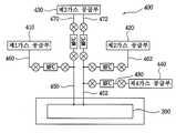
도 1은 본 발명의 일 실시예에 따른 금속 산화물 형성 장치를 설명하기 위한 개략적인 구성도이다.1 is a schematic configuration diagram illustrating a metal oxide forming apparatus according to an embodiment of the present invention.
도 1을 참조하면, 금속 산화물 형성 장치(100)는 실리콘웨이퍼와 같은 반도체 기판(10) 상에 고유전율을 갖는 금속 산화물을 형성하기 위하여 사용될 수 있다. 특히, 하프늄 산화물(HfO), 지르코늄 산화물(ZrO), 알루미늄 산화물(AlO), 탄탈륨 산화물(TaO), 티타늄 산화물(TiO), 란탄 산화물(LaO), 스트론튬 산화물(SrO), 바륨 산화물(BaO), 프라세오디뮴 산화물(PrO), 납 산화물(PbO) 등과 같은 금속 산화물을 형성하기 위하여 사용될 수 있다. 상기 금속 산화물로 이루어진 막은 트랜지스터의 게이트 절연막 또는 커패시터의 유전막 등으로 사용될 수 있다.Referring to FIG. 1, the metal
상기 반도체 기판(10)은 스테이지(200) 상에 지지될 수 있으며, 상기 스테이지(200)는 상기 반도체 기판(10)을 지지하기 위한 지지영역(210)과 상기 지지영 역(210)을 둘러싸는 주변영역(220)을 가질 수 있다. 상기 주변영역(220)의 상부면은 상기 지지영역(210)의 상부면보다 높게 위치될 수 있다. 예를 들면, 상기 주변영역(220)의 상부면은 상기 지지영역(210) 상에 위치된 반도체 기판(10)의 상부면과 실질적으로 동일한 높이를 가질 수 있도록 배치될 수 있다.The
상기 스테이지(200)의 내부에는 상기 반도체 기판(10)을 공정 온도로 가열하기 위한 히터(230)가 배치될 수 있다. 그러나, 이와는 다르게, 상기 스테이지(200)의 하부에 상기 반도체 기판(10)을 가열하기 위한 히팅 블록이 결합될 수도 있다. 예를 들면, 상기 금속 산화물은 상온 내지 약 450℃의 온도에서 형성될 수 있다.A
상기 스테이지(200)의 주변영역(220) 상에는 상기 반도체 기판(10)이 위치되는 공간을 한정하기 위한 공정 챔버(300)가 배치될 수 있다. 상기 공정 챔버(300)는 커버(310)와 RF 전극(350)을 포함할 수 있다.The
상기 커버(310)는 상기 스테이지(200)의 상부에 배치되는 천장부(320)와, 상기 천장부(320)로부터 하방으로 연장하며 상기 스테이지(200)의 주변영역(220) 상에 배치되는 링 형태의 돌출부(330)를 포함할 수 있으며, 상기 RF 전극(350)은 상기 스테이지(200)의 지지영역(210) 상에 위치된 반도체 기판(10)과 마주하도록 상기 천장부(320)의 하부면 상에 배치된다. 도시되지는 않았으나, 상기 RF 전극(350)은 다수의 체결 부재들에 의해 상기 천장부(320)의 하부면 상에 결합될 수 있다.The
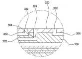
도 2는 가스 도입구를 설명하기 위한 확대 단면도이며, 도 3은 배기구를 설명하기 위한 확대 단면도이다.2 is an enlarged cross-sectional view for explaining the gas inlet, and FIG. 3 is an enlarged cross-sectional view for explaining the exhaust port.
도 2 및 도 3을 참조하면, 상기 공정 챔버(300)는 상기 반도체 기판(10) 상 으로 금속 전구체 가스와 오존을 포함하는 산화 가스를 공급하기 위한 가스 도입구(302) 및 상기 가스들을 배출하기 위한 배기구(304)를 갖는다.2 and 3, the
상기 가스 도입구(302)는 상기 반도체 기판(10)의 제1 가장자리 부위와 인접하여 배치되며, 상기 배기구(304)는 상기 반도체 기판(10)의 제1 가장자리 부위에 대향하는 제2 가장자리 부위와 인접하여 배치된다.The
상기 가스 도입구(302)는 상기 돌출부(330)의 제1 내측면(332)과 상기 RF 전극(350)의 제1 외측면(352)에 의해 한정될 수 있으며, 상기 배기구(304)는 상기 돌출부(330)의 제2 내측면(334)과 상기 RF 전극(350)의 제2 외측면(354)에 의해 한정될 수 있다. 상기 돌출부(330)의 제1 내측면(332)과 제2 내측면(334)은 서로 마주하여 배치되며 상기 RF 전극(350)의 제1 외측면(352)과 제2 외측면(354)은 서로 반대 방향으로 배치된다.The
상기 금속 전구체 가스는 상기 가스 도입구(302)로부터 상기 반도체 기판(10)의 표면을 따라 상기 배기구(304)를 향하여 흐르며, 이에 따라 상기 반도체 기판(10) 상에는 금속 전구체 막이 형성될 수 있다. 상기 산화 가스는 상기 반도체 기판(10) 상에 형성된 금속 전구체 막을 따라 상기 가스 도입구(302)로부터 상기 배기구(304)를 향하여 흐르며, 이에 따라 상기 금속 전구체 막과 상기 산화 가스 사이의 반응에 의해 상기 기판(10) 상에는 금속 산화물 막이 형성된다. 즉, 상기 금속 전구체 가스 및 상기 산화 가스는 상기 반도체 기판(10)의 제1 가장자리 부위로부터 제2 가장자리 부위를 향하여 흐르도록 공급된다.The metal precursor gas flows from the
다시 도 1을 참조하면, 상기 금속 전구체 가스 및 산화 가스를 공급하기 위 한 가스 공급부(400)는 가스 공급 배관들을 통해 공정 챔버(300)의 천장부(320)와 연결되며, 상기 가스들과 상기 금속 산화물을 형성하는 동안 발생된 반응 부산물들은 상기 공정 챔버(300)의 천장부(320)와 배기 배관을 통해 연결된 배기부(500)에 의해 공정 챔버(300)로부터 제거될 수 있다.Referring back to FIG. 1, the
도 4는 가스 공급부를 설명하기 위한 개략적인 구성도이다.4 is a schematic diagram illustrating a gas supply unit.
도 4를 참조하면, 가스 공급부(400)는 상기 금속 전구체 가스를 공급하기 위한 제1 가스 공급부(410)와 상기 산화 가스를 공급하기 위한 제2 가스 공급부(420)를 포함할 수 있다.Referring to FIG. 4, the
예를 들면, 상기 제1 가스 공급부(410)로는 분무기 및 기화기를 포함하는 액체 전달 시스템(Liquid Delivery System; LDS) 또는 버블링 용기를 포함하는 버블러(bubbler)가 사용될 수 있다.For example, a liquid delivery system (LDS) including a nebulizer and a vaporizer or a bubbler including a bubbling vessel may be used as the first
상기 금속 전구체 가스는 Zr, Hf, Al, Ta, Ti, La, Sr, Ba, Pr, Pb 등과 같은 금속을 포함할 수 있으며, 캐리어 가스와 함께 상기 공정 챔버(300)로 공급될 수 있다. 상기 캐리어 가스로는 아르곤(Ar) 가스와 같은 불활성 가스가 사용될 수 있다.The metal precursor gas may include a metal such as Zr, Hf, Al, Ta, Ti, La, Sr, Ba, Pr, Pb, and the like, and may be supplied to the
상기 제2 가스 공급부(420)는 오존 발생기를 포함할 수 있다. 상기 오존 발생기는 산소 가스를 이용하여 오존을 발생시킬 수 있다. 즉, 상기 오존 발생기로부터 공급되는 산화 가스는 산소와 오존의 혼합 가스이며, 상기 산화 가스의 오존 농도는 약 100 내지 1000g/m3 정도의 범위 내에 있을 수 있다. 특히, 상기 산화 가스 의 오존 농도는 약 100 내지 500g/m3 정도의 범위 내에 있을 수 있다. 예를 들면, 약 200 정도의 오존 농도를 갖는 산화 가스가 사용될 수 있다.The second
상기 가스 공급부(400)는 퍼지 가스와 압력 조절용 가스로서 사용되는 불활성 가스를 공급하기 위한 제3 가스 공급부(430)를 더 포함할 수 있다. 구체적으로, 상기 공정 챔버(300)의 내부는 상기 금속 전구체 막을 형성한 후 퍼지 가스에 의해 일차 퍼지되며, 상기 금속 산화물을 형성한 후 퍼지 가스에 의해 이차 퍼지될 수 있다. 또한, 상기 금속 산화물 막을 형성하는 동안 상기 공정 챔버(300) 내부의 압력은 약 0.1 내지 10Torr 정도의 압력으로 유지될 수 있으며, 상기 압력 조절용 가스는 상기 공정 챔버(300) 내부의 압력 조절을 위하여 상기 금속 전구체 가스 및 상기 산화 가스와 함께 상기 공정 챔버(300) 내부로 공급된다.The
또한, 상기 가스 공급부(400)는 상기 일차 퍼지 단계를 수행한 후 상기 공정 챔버 내부에 산소 가스를 공급하기 위한 제4 가스 공급부(440)를 더 포함할 수 있다. 상기 제4 가스 공급부(440)는 상기 산화 가스를 이용한 상기 금속 전구체 막의 산화 단계가 수행되기 전에 공정 챔버(300) 내부를 산소 분위기로 형성하기 위하여 제공될 수 있다. 도시된 바에 의하면, 상기 공정 챔버 내부에 산소 가스를 공급하기 위한 제4 가스 공급부(440)가 제공되고 있으나, 상기 산소 가스는 제2 공급부(420)에 의해 제공될 수도 있다.In addition, the
상기 제1, 제2, 제3 및 제4 가스 공급부들(410, 420, 430, 440)은 다수의 배관들에 의해 상기 공정 챔버(300)와 연결될 수 있다. 상기 공정 챔버(300)에는 제1 주 배관(450) 및 제2 주 배관(452)이 연결되어 있으며, 상기 제1 가스 공급부(410)는 상기 제1 주 배관(450)으로부터 분기된 제1 분기 배관(460)에 연결되어 있고, 제2 가스 공급부(420)는 상기 제2 주 배관(452)으로부터 분기된 제2 분기 배관(462)에 연결되어 있다. 상기 제3 가스 공급부(430)는 상기 제1 및 제2 메인 배관들(450, 452)로부터 각각 분기된 제3 및 제4 분기 배관들(470, 472)과 연결되어 있으며, 상기 제4 가스 공급부(440)는 연결 배관(480)을 통해 상기 제2 주 배관(452)과 연결되어 있다.The first, second, third and fourth gas supplies 410, 420, 430, and 440 may be connected to the
상기 제1, 제2, 제3 및 제4 분기 배관들(460, 462, 470, 472) 및 상기 연결 배관(480)에는 상기 금속 전구체 가스, 산화 가스, 퍼지 가스, 압력 조절용 가스 및 산소 가스의 공급 유량을 제어하기 위한 다수의 유량 제어기들과 밸브들이 설치될 수 있다.The first, second, third and
그러나, 상기 배관들, 유량 제어기들 및 밸브들의 구성은 다양하게 변경될 수 있으며, 상기에서 설명된 상기 배관들, 유량 제어기들 및 밸브들의 연결 관계가 본 발명의 범위를 한정하지는 않는다.However, the configuration of the pipes, flow controllers and valves can be variously changed, and the connection relationship of the pipes, flow controllers and valves described above does not limit the scope of the present invention.
다시 도 1을 참조하면, 상기 공정 챔버(300)와 스테이지(200)는 외측 챔버(600)에 내에 수용될 수 있으며, 외측 챔버(600)의 하부에는 상기 스테이지(200)를 회전시키기 위한 제1 구동부(700)와 상기 스테이지(200)를 수직 방향으로 이동시키기 위한 제2 구동부(800)가 배치될 수 있다.Referring back to FIG. 1, the
상기 제1 구동부(700)는 상기 금속 산화물 막을 형성하는 동안 상기 금속 산화물 막의 두께 균일도를 향상시키기 위하여 상기 스테이지(200)를 기 설정된 각도 만큼 단계적으로 회전시킬 수 있다. 예를 들면, 상기 금속 전구체 막의 형성 단계, 상기 일차 퍼지 단계, 상기 금속 전구체 막의 산화 단계 및 상기 이차 퍼지 단계를 수행한 후, 상기 스테이지(200)를 기 설정된 각도, 예를 들면, 약 90° 또는 약 180° 회전시킬 수 있다. 이어서, 상기 단계들을 반복적으로 수행함으로써 결과적으로 형성되는 금속 산화물 막의 두께 균일도를 향상시킬 수 있다.The
이와는 다르게, 상기 제1 구동부(700)는 상기 단계들을 반복적으로 수행하는 동안 상기 반도체 기판(10)을 연속적으로 회전시킬 수도 있다.Alternatively, the
상기 제1 구동부(700)는 상기 스테이지(200)를 이동시키지 않으면서 상기 단계들을 반복적으로 수행하기 위하여 상기 반도체 기판(10)이 위치되는 상기 스테이지(200)의 지지영역(210)만 선택적으로 회전시킬 수 있다.The
상기 제2 구동부(800)는 상기 반도체 기판(10)의 로딩 및 언로딩을 위하여 상기 스테이지(200)를 수직 방향으로 이동시킬 수 있다.The
도시되지는 않았으나, 상기 반도체 기판(10)의 로딩 및 언로딩을 위하여 상기 스테이지(200)를 통해 수직 방향으로 이동 가능하게 배치되는 다수의 리프트 핀들이 상기 외측 챔버(600) 내에 배치될 수 있으며, 상기 외측 챔버(600)의 측벽에는 반도체 기판(10)의 이송을 위한 게이트 밸브가 설치될 수 있다.Although not shown, a plurality of lift pins movably disposed in the vertical direction through the
한편, 상기 배기부(500)는 상기 금속 산화물 막을 형성하는 동안 발생되는 반응 부산물들과 상기 가스들을 배출하기 위하여 상기 공정 챔버(300)와 연결된다.Meanwhile, the
상기 배기부(500)는 고진공 펌프와 러핑 펌프를 포함할 수 있으며, 상기 금속 산화물 막을 형성하는 동안 상기 공정 챔버(300) 내부는 상기 배기부(500)에 의 해 약 0.1 내지 10 Torr 정도의 압력으로 유지될 수 있다.The
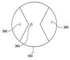
도 5는 도 1에 도시된 RF 전극을 설명하기 위한 확대 단면도이고, 도 6은 도 1에 도시된 RF 전극을 설명하기 위한 평면도이다.5 is an enlarged cross-sectional view for explaining the RF electrode shown in FIG. 1, and FIG. 6 is a plan view for explaining the RF electrode shown in FIG. 1.
도 2, 도 3, 도 5 및 도 6을 참조하면, 상기 커버(310)의 천장부(320)는 상기 금속 전구체 가스의 공급을 위한 제1 연결구(322)와, 상기 산화 가스의 공급을 위한 제2 연결구(324) 및 상기 배기부(500)와의 연결을 위한 제3 연결구(326)를 갖는다.2, 3, 5, and 6, the
상기 RF 전극(350)의 상부면에는 상기 제1 연결구(322)와 연통하며 상기 제1 외측면(352)을 향하여 확장된 제1 유로(360)가 형성되어 있다. 상기 RF 전극(350)의 내부에는 상기 제1 외측면(352)을 향하여 확장된 제2 유로(362)가 형성되어 있으며, 상기 확장된 제2 유로(362)는 제4 연결구(364)를 통해 상기 제2 연결구(324)와 연통된다. 또한, 상기 RF 전극(350)의 상부면에는 상기 제3 연결구(326)와 연통하며 상기 제2 외측면(354)을 향하여 확장된 제3 유로(366)가 형성되어 있다. 상기 제1, 제2 및 제3 유로들(360, 362, 366)은 도시된 바와 같이 각각 부채꼴 형태로 확장될 수 있다.A
도시된 바에 의하면, 상기 제1 유로(360)와 제3 유로(366)는 상기 RF 전극(350)의 상부면 부위들에 형성되어 있으나, 상기 제2 유로(362)와 같이 상기 RF 전극(350)의 내부에 형성될 수도 있다.As illustrated, although the
상기와 같이 제1 및 제2 유로들(360, 362)이 상기 제1 외측면(352)을 향하여 확장되므로, 상기 금속 전구체 가스 및 상기 산화 가스는 상기 반도체 기판(10)의 표면 및 상기 금속 전구체 막의 표면을 따라 균일하게 공급될 수 있다.Since the first and
다시 도 1을 참조하면, 상기 RF 전극(350)은 상기 금속 전구체 막의 표면을 따라 흐르는 산화 가스에 RF 파워를 인가하기 위하여 RF 파워 소스(900)와 연결되어 있다. 상기 RF 파워는 상기 금속 전구체 막과 상기 산화 가스 사이의 산화 반응을 촉진시키기 위하여 인가된다. 즉, 상기 오존을 포함하는 상기 산화 가스에 RF 파워를 인가함으로써 상기 산화 가스의 오존 농도를 증가시킬 수 있으며, 이에 따라 상기 금속 전구체 막과 직접적으로 반응하는 산소 라디칼의 농도가 증가될 수 있다. 결과적으로, 상기 금속 전구체 막과 상기 산화 가스 사이의 반응이 촉진될 수 있다.Referring back to FIG. 1, the
도 7은 도 1에 도시된 금속 산화물 형성 장치를 이용하여 반도체 기판 상에 금속 산화물 막을 형성하는 방법을 설명하기 위한 순서도이다.FIG. 7 is a flowchart illustrating a method of forming a metal oxide film on a semiconductor substrate using the metal oxide forming apparatus shown in FIG. 1.
도 7을 참조하면, 단계 S100에서, 실리콘웨이퍼와 같은 반도체 기판(10)을 스테이지(200) 상에 위치시킨다. 구체적으로, 상기 반도체 기판(10)은 외측 챔버(600)의 게이트 밸브를 통해 상기 외측 챔버(600) 내부로 이송될 수 있으며, 다수의 리프트 핀들에 의해 상기 스테이지(200) 상에 놓여질 수 있다. 이어서, 상기 제2 구동부(800)는 상기 반도체 기판(10)을 상기 공정 챔버(300) 내에 위치시키기 위하여 상기 스테이지(200)를 상방으로 이동시킨다.Referring to FIG. 7, in step S100, a
상기 반도체 기판(10) 상에는 전기적 특성을 갖는 패턴들이 형성되어 있을 수 있다. 예를 들면, 상기 반도체 기판(10)의 표면 부위에는 필드 절연막에 의해 전기적으로 절연된 액티브 패턴들이 형성되어 있을 수 있다. 또한, 상기 반도체 기 판(10) 상에는 커패시터들의 하부 전극들로서 기능하는 실린더 형태의 도전성 구조물들이 형성되어 있을 수 있다.Patterns having electrical characteristics may be formed on the
단계 S200에서, 상기 반도체 기판(10)의 표면을 따라 금속 전구체 가스를 공급하여 반도체 기판(10) 상에 금속 전구체 막을 형성한다. 상기 금속 전구체 가스는 제1 가스 공급부(410)에 의해 상기 제1 유로(360) 및 가스 도입구(302)를 통해 상기 반도체 기판(10) 상으로 공급될 수 있다. 상기 금속 전구체 가스는 Zr, Hf, Al, Ta, Ti, La, Sr, Ba, Pr, Pb 등과 같은 금속을 포함할 수 있다. 예를 들면, 지르코늄을 포함하는 금속 전구체 가스로서 TEMAZ(tetrakis ethyl methyl amino zirconium, Zr[N(CH3)(C2H5)]4), 지르코늄 부틸옥사이드(Zr(O-tBu)4) 또는 이들의 혼합물이 사용될 수 있으며, 하프늄을 포함하는 금속 전구체 가스로서 TDMAH(tetrakis dimethyl amino hafnium, Hf[N(CH3)2]4), TEMAH(tetrakis ethyl methyl amino hafnium, Hf[N(C2H5)CH3]4), TDEAH(tetrakis diethyl amino hafnium, Hf[N(C2H5)2]4), Hf[OC(CH3)2CH2OCH3]4, Hf[OC(CH3)3]4 등이 사용될 수 있으며, 이들의 혼합물이 사용될 수도 있다.In step S200, a metal precursor gas is supplied along the surface of the
상기 금속 전구체 가스는 분무기를 이용하여 액상의 금속 전구체를 에어로졸 미스트로 형성하고, 기화기를 이용하여 상기 에어로졸 미스트를 기화시킴으로써 형성될 수 있다. 이와 다르게, 상기 금속 전구체 가스는 캐리어 가스를 액상의 금속 전구체 내에서 버블링시킴으로써 형성될 수도 있다.The metal precursor gas may be formed by forming a liquid metal precursor into an aerosol mist using an atomizer, and vaporizing the aerosol mist using a vaporizer. Alternatively, the metal precursor gas may be formed by bubbling a carrier gas in a liquid metal precursor.
상기 금속 전구체 가스가 상기 반도체 기판(10)의 표면을 따라 흐르는 동안, 상기 반도체 기판(10)의 표면 상에는 금속 전구체 막이 형성된다. 상기 금속 전구체 막은 상기 반도체 기판(10)의 표면 상에 화학적으로 흡착된 원자막일 수 있으며, 또한 상기 금속 전구체 원자막 상에 물리적으로 흡착된 제2 막이 형성될 수 있다.While the metal precursor gas flows along the surface of the
단계 S300에서, 상기 공정 챔버(300) 내부로 퍼지 가스를 공급한다. 상기 퍼지 가스는 제3 가스 공급부(430)로부터 상기 제1 유로(360), 제2 유로(362) 및 가스 도입구(302)를 통해 상기 공정 챔버(300) 내부로 공급될 수 있다. 상기 제2 막은 상기 퍼지 가스의 공급 및 상기 배기부(500)에 의한 진공 배기에 의해 상기 금속 전구체 원자막으로부터 제거될 수 있으며, 상기 공정 챔버(300) 내부에 잔류하는 금속 전구체 가스 역시 상기 퍼지 가스와 함께 상기 공정 챔버(300)로부터 제거될 수 있다.In step S300, a purge gas is supplied into the
단계 S400에서, 상기 금속 전구체 막의 표면을 따라 오존을 포함하는 산화 가스를 공급하여 상기 금속 전구체 막을 산화시킨다. 상기 산화 가스는 제2 가스 공급부(420)로부터 제2 유로(362) 및 가스 도입구(302)를 통해 공급될 수 있다.In step S400, an oxidizing gas including ozone is supplied along the surface of the metal precursor film to oxidize the metal precursor film. The oxidizing gas may be supplied from the second
단계 S500에서, 상기 금속 전구체 막과 상기 산화 가스 사이의 반응을 촉진시키기 위하여 RF 파워를 인가한다. 상기 RF 파워는 RF 파워 소스(900)와 연결된 RF 전극(350)에 의해 상기 금속 전구체 막의 표면을 따라 흐르는 산화 가스에 인가될 수 있다. 상기 RF 파워를 인가함으로써 상기 산화 가스의 산소 라디칼 농도가 증가될 수 있으며, 이에 따라 상기 금속 전구체 막과 상기 산화 가스 사이의 반응이 촉진될 수 있다.In step S500, RF power is applied to promote a reaction between the metal precursor film and the oxidizing gas. The RF power may be applied to the oxidizing gas flowing along the surface of the metal precursor film by the
결과적으로, 상기 반도체 기판(10) 상에는 향상된 전기적 특성을 갖는 금속 산화물 막이 형성될 수 있다. 특히, 상기한 바와 같은 본 발명의 실시예에 따른 금속 산화물 형성 방법은 반도체 기판(10) 상에 고종횡비를 갖는 실린더 형태의 하부 전극들이 형성되어 있는 경우에 유용하게 사용될 수 있다.As a result, a metal oxide film having improved electrical characteristics may be formed on the
도시된 바에 의하면, 상기 단계들 S400 및 S500은 순차적으로 수행되고 있으나, 상기 단계들 S400 및 S500은 동시에 수행될 수도 있다.As shown, the steps S400 and S500 are performed sequentially, but the steps S400 and S500 may be performed simultaneously.
또한, 상기 단계 S400을 수행하기 전에 단계 S350을 더 수행할 수도 있다. 상기의 단계 S350에서, 상기 금속 전구체 막 상으로 산소 가스가 공급될 수 있다. 상기 산소 가스는 공정 챔버(300)로부터 퍼지 가스를 제거하기 위하여 그리고 상기 공정 챔버(300) 내부를 산소 분위기로 형성하기 위하여 제공될 수 있다. 예를 들면, 상기 산소 가스는 제4 가스 공급부(440)로부터 제2 유로(362) 및 가스 도입구(302)를 통해 약 0.1 내지 3초 동안 공급될 수 있다.In addition, step S350 may be further performed before performing step S400. In the above step S350, oxygen gas may be supplied onto the metal precursor film. The oxygen gas may be provided to remove the purge gas from the
단계 S600에서, 상기 공정 챔버(300) 내부로 퍼지 가스를 공급한다. 상기 퍼지 가스는 제3 가스 공급부(430)로부터 상기 제1 유로(360), 제2 유로(362) 및 가스 도입구(302)를 통해 상기 공정 챔버(300) 내부로 공급될 수 있다. 상기 공정 챔버 내부(300)에 잔류하는 산화 가스 및 반응 부산물들은 상기 퍼지 가스와 함께 상기 배기구(304) 및 상기 제3 유로(366)를 통해 상기 공정 챔버로부터 제거될 수 있다.In step S600, a purge gas is supplied into the
상기 단계들을 수행하는 동안 상기 반도체 기판(10)은 기 설정된 공정 온도로 가열될 수 있다. 예를 들면, 상기 반도체 기판(10)은 상기 히터(230)에 의해 약 450℃ 이하의 온도로 가열될 수 있다. 또한, 상기 단계들을 수행하는 동안 상기 공정 챔버(300) 내부의 압력은 약 0.1 내지 10Torr 정도로 유지될 수 있다. 예를 들면, 상기 공정 챔버(300) 내부의 압력은 상기 제3 가스 제공부(430)로부터 공급되는 압력 조절용 가스와 배기부(500)에 의해 약 3Torr 정도에서 유지될 수 있다.During the steps, the
단계 S700에서, 상기 반도체 기판(10)을 기 설정된 각도만큼 회전시킨다. 예를 들면, 상기 반도체 기판(10)은 제1 구동부(700)에 의해 약 90° 또는 약 180°의 각도만큼 회전될 수 있다.In operation S700, the
단계 S800에서, 상기 단계들 S200 내지 S600을 반복적으로 수행한다. 상기 단계들 S700 및 S800은 상기 반도체 기판(10) 상에 목적하는 두께를 갖는 금속 산화물 막이 형성될 때까지 반복적으로 수행될 수 있다. 결과적으로, 상기 반도체 기판(10) 상에는 균일한 두께와 향상된 전기적 특성을 갖는 금속 산화물 막이 형성될 수 있다.In step S800, the steps S200 to S600 are repeatedly performed. The steps S700 and S800 may be repeatedly performed until a metal oxide film having a desired thickness is formed on the
그러나, 상기 반도체 기판(10)은 상기 단계들 S200 내지 S600을 반복적으로 수행하는 동안 기 설정된 회전 속도로 연속적으로 회전할 수도 있다.However, the
상기와 같은 본 발명의 실시예에 따라 형성된 금속 산화물 막의 전기적 특성을 검사하기 위하여 다음과 같은 실험들을 수행하였다.In order to examine the electrical properties of the metal oxide film formed according to the embodiment of the present invention as described above were carried out the following experiments.
비교예 1Comparative Example 1
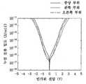
산소 플라즈마를 이용하는 일반적인 플라즈마 강화 원자층 증착을 이용하여 실린더 형태의 하부 전극들이 형성된 반도체 기판 상에 제1 하프늄 산화물 막을 형성하였다. 상기 제1 하프늄 산화물 막을 형성하는 동안 공정 온도는 300℃에서 유 지되었으며, 공정 챔버의 내부 압력은 3Torr에서 유지되었다. 상기 제1 하프늄 산화물 막을 통한 누설 전류는 상기 반도체 기판의 중앙 부위, 왼쪽 부위 및 오른쪽 부위에서 각각 측정되었으며, 그 결과는 도 8에 도시되었다.A first hafnium oxide film was formed on a semiconductor substrate on which cylindrical lower electrodes were formed by using general plasma enhanced atomic layer deposition using an oxygen plasma. The process temperature was maintained at 300 ° C. and the internal pressure of the process chamber was maintained at 3 Torr during the formation of the first hafnium oxide film. The leakage current through the first hafnium oxide film was measured at the center portion, the left portion and the right portion of the semiconductor substrate, respectively, and the results are shown in FIG. 8.
비교예 2Comparative Example 2
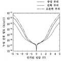
오존을 포함하는 산화 가스를 이용하는 플라즈마 강화 원자층 증착을 이용하여 실린더 형태의 하부 전극들이 형성된 반도체 기판 상에 제2 하프늄 산화물 막을 형성하였다. 상기 제2 하프늄 산화물 막을 형성하는 동안 공정 온도는 300℃에서 유지되었으며, 공정 챔버 내부의 압력은 3Torr 정도로 유지되었다. 상기 제2 하프늄 산화물 막을 통한 누설 전류는 상기 반도체 기판의 중앙 부위, 왼쪽 부위 및 오른쪽 부위에서 각각 측정되었으며, 그 결과는 도 9에 도시되었다.A second hafnium oxide film was formed on a semiconductor substrate on which cylindrical lower electrodes were formed using plasma enhanced atomic layer deposition using an oxidizing gas containing ozone. The process temperature was maintained at 300 ° C. and the pressure inside the process chamber was maintained at about 3 Torr during the formation of the second hafnium oxide film. The leakage current through the second hafnium oxide film was measured at the center portion, the left portion and the right portion of the semiconductor substrate, respectively, and the results are shown in FIG. 9.
도 8 및 도 9를 참조하면, 상기 제1 하프늄 산화물 막의 중앙 부위에서의 등가 산화막 두께는 약 20.1Å으로 측정되었고, 왼쪽 부위 및 오른쪽 부위에서는 각각 약 19.1Å 및 19.6Å 정도의 등가 산화막 두께들이 측정되었다.8 and 9, the equivalent oxide film thickness at the center portion of the first hafnium oxide film was measured to be about 20.1
상기 제2 하프늄 산화물 막의 중앙 부위에서의 등가 산화막 두께는 약 29.8Å으로 측정되었고, 왼쪽 부위 및 오른쪽 부위에서는 각각 약 28.7Å 및 28.6Å 정도의 등가 산화막 두께들이 측정되었다.The equivalent oxide film thickness at the central portion of the second hafnium oxide film was measured to be about 29.8 kPa, and the equivalent oxide film thicknesses of about 28.7 kPa and 28.6 kPa were measured at the left and right portions, respectively.
상기 제1 하프늄 산화물 막을 통한 누설 전류 특성은 상기 제2 하프늄 산화물 막에 비하여 열악하며, 상기 제2 하프늄 산화물 막은 상기 제1 하프늄 산화물 막에 비하여 우수한 누설 전류 특성을 갖고 있지만, 누설 전류 분포가 매우 열악함을 알 수 있다.The leakage current characteristic through the first hafnium oxide film is inferior to the second hafnium oxide film, and the second hafnium oxide film has better leakage current characteristics than the first hafnium oxide film, but the leakage current distribution is very poor. It can be seen.
실시예 1Example 1
본 발명의 실시예에 따른 방법을 이용하여 실린더 형태의 하부 전극들이 형성된 반도체 기판 상에 제3 하프늄 산화물 막을 형성하였다.A third hafnium oxide film was formed on a semiconductor substrate on which cylindrical lower electrodes were formed by using the method according to the exemplary embodiment of the present invention.
상기 제3 하프늄 산화물 막을 형성하기 위하여 약 200g/m3 정도의 오존 농도를 갖는 산화 가스가 사용되었으며, 약 250W 정도의 RF 파워가 RF 전극을 통해 인가되었다. 또한, 공정 온도는 약 300℃ 정도로 유지되었으며, 공정 챔버의 내부 압력은 약 3Torr 정도로 유지되었다.An oxidizing gas having an ozone concentration of about 200 g / m3 was used to form the third hafnium oxide film, and RF power of about 250 W was applied through the RF electrode. In addition, the process temperature was maintained at about 300 ℃ and the internal pressure of the process chamber was maintained at about 3 Torr.
상기 제3 하프늄 산화물 막을 통한 누설 전류는 상기 반도체 기판의 중앙 부위, 왼쪽 부위 및 오른쪽 부위에서 각각 측정되었으며, 그 결과는 도 10에 도시되었다.The leakage current through the third hafnium oxide film was measured at the center portion, the left portion and the right portion of the semiconductor substrate, respectively, and the results are shown in FIG. 10.
도 10을 참조하면, 상기 제3 하프늄 산화물 막의 중앙 부위에서의 등가 산화막 두께는 약 19.5Å으로 측정되었고, 왼쪽 부위 및 오른쪽 부위에서는 각각 약 20.1Å 및 19.5Å 정도의 등가 산화막 두께들이 측정되었다.Referring to FIG. 10, the equivalent oxide film thickness at the central portion of the third hafnium oxide film was measured to be about 19.5 kPa, and the equivalent oxide film thicknesses of about 20.1 kPa and 19.5 kPa were measured at the left and right portions, respectively.
도시된 바와 같이 상기 제3 하프늄 산화물 막은 제1 하프늄 산화물 막과 유사한 등가 산화막 두께들을 갖고 있으며, 제1 하프늄 산화물 막과 비교하여 개선된 누설 전류 특성을 갖고 있음을 알 수 있다.As shown, it can be seen that the third hafnium oxide film has equivalent oxide film thicknesses similar to the first hafnium oxide film and has improved leakage current characteristics compared to the first hafnium oxide film.
한편, 제2 하프늄 산화물 막의 등가 산화막 두께들이 제3 하프늄 산화물 막에 비하여 두껍기 때문에 상기 제3 하프늄 산화물 막을 제2 하프늄 산화막과 직접적으로 비교하기는 어렵지만, 도시된 바에 의하면, 제3 하프늄 산화물 막이 제2 하 프늄 산화물 막에 비하여 누설 전류 분포가 개선되었음을 충분히 알 수 있다.On the other hand, since the equivalent oxide film thickness of the second hafnium oxide film is thicker than that of the third hafnium oxide film, it is difficult to directly compare the third hafnium oxide film to the second hafnium oxide film. It can be seen that the leakage current distribution is improved compared to the hafnium oxide film.
상기 제1, 제2 및 제3 하프늄 산화물 막들의 직접적인 비교를 위하여 전계(인가된 전압/등가 산화막 두께) 변화에 따른 누설 전류의 변화를 비교하였으며, 그 결과를 도 11에 도시하였다.In order to directly compare the first, second and third hafnium oxide films, changes in leakage current according to electric field (applied voltage / equivalent oxide film thickness) change were compared, and the results are shown in FIG. 11.
도 11을 참조하면, 상기 제3 하프늄 산화물 막의 누설 전류 특성이 상기 제1 및 제2 하프늄 산화물 막들에 비하여 크게 개선되었음을 알 수 있다.Referring to FIG. 11, it can be seen that the leakage current characteristics of the third hafnium oxide film are significantly improved compared to the first and second hafnium oxide films.
실시예 2Example 2
본 발명의 실시예에 따른 방법을 이용하여 실린더 형태의 하부 전극들이 형성된 반도체 기판 상에 제4 하프늄 산화물 막을 형성하였다. 상기 제4 하프늄 산화막을 형성하는 동안 약 100W의 RF 파워가 RF 전극을 통해 인가되었으며 약 100sccm 정도의 유량으로 오존을 포함하는 산화 가스가 공급되었다. 또한, 공정 온도는 약 300℃ 정도로 유지되었으며, 공정 챔버 내부의 압력은 약 3Torr 정도로 유지되었다.A fourth hafnium oxide film was formed on a semiconductor substrate on which cylindrical lower electrodes were formed by using the method according to the exemplary embodiment of the present invention. During the formation of the fourth hafnium oxide film, about 100 W of RF power was applied through the RF electrode, and an oxidizing gas including ozone was supplied at a flow rate of about 100 sccm. In addition, the process temperature was maintained at about 300 ℃ and the pressure inside the process chamber was maintained at about 3 Torr.
실시예 3Example 3
본 발명의 실시예에 따른 방법을 이용하여 실린더 형태의 하부 전극들이 형성된 반도체 기판 상에 제5 하프늄 산화물 막을 형성하였다. 상기 제5 하프늄 산화막을 형성하는 동안 약 100W의 RF 파워가 RF 전극을 통해 인가되었으며 약 500sccm 정도의 유량으로 오존을 포함하는 산화 가스가 공급되었다. 또한, 공정 온도는 약 300℃ 정도로 유지되었으며, 공정 챔버 내부의 압력은 약 3Torr 정도로 유지되었다.A fifth hafnium oxide film was formed on a semiconductor substrate on which cylindrical lower electrodes were formed by using the method according to the exemplary embodiment of the present invention. During the formation of the fifth hafnium oxide film, about 100 W of RF power was applied through the RF electrode, and an oxidizing gas including ozone was supplied at a flow rate of about 500 sccm. In addition, the process temperature was maintained at about 300 ℃ and the pressure inside the process chamber was maintained at about 3 Torr.
실시예 4Example 4
본 발명의 실시예에 따른 방법을 이용하여 실린더 형태의 하부 전극들이 형성된 반도체 기판 상에 제6 하프늄 산화물 막을 형성하였다. 상기 제6 하프늄 산화막을 형성하는 동안 약 250W의 RF 파워가 RF 전극을 통해 인가되었으며 약 100sccm 정도의 유량으로 오존을 포함하는 산화 가스가 공급되었다. 또한, 공정 온도는 약 300℃ 정도로 유지되었으며, 공정 챔버 내부의 압력은 약 3Torr 정도로 유지되었다.The sixth hafnium oxide film was formed on a semiconductor substrate on which cylindrical lower electrodes were formed by using the method according to the exemplary embodiment of the present invention. During the formation of the sixth hafnium oxide film, about 250 W of RF power was applied through the RF electrode, and an oxidizing gas including ozone was supplied at a flow rate of about 100 sccm. In addition, the process temperature was maintained at about 300 ℃ and the pressure inside the process chamber was maintained at about 3 Torr.
실시예 5Example 5
본 발명의 실시예에 따른 방법을 이용하여 실린더 형태의 하부 전극들이 형성된 반도체 기판 상에 제7 하프늄 산화물 막을 형성하였다. 상기 제7 하프늄 산화막을 형성하는 동안 약 250W의 RF 파워가 RF 전극을 통해 인가되었으며 약 500sccm 정도의 유량으로 오존을 포함하는 산화 가스가 공급되었다. 또한, 공정 온도는 약 300℃ 정도로 유지되었으며, 공정 챔버 내부의 압력은 약 3Torr 정도로 유지되었다.A seventh hafnium oxide film was formed on a semiconductor substrate on which cylindrical lower electrodes were formed by using the method according to the exemplary embodiment of the present invention. During the formation of the seventh hafnium oxide film, about 250 W of RF power was applied through the RF electrode, and an oxidizing gas including ozone was supplied at a flow rate of about 500 sccm. In addition, the process temperature was maintained at about 300 ℃ and the pressure inside the process chamber was maintained at about 3 Torr.
상기 제4, 제5, 제6 및 제7 하프늄 산화물 막들을 통한 누설 전류 특성들을 측정하였으며, 그 결과는 도 12에 도시하였다.Leakage current characteristics through the fourth, fifth, sixth and seventh hafnium oxide films were measured, and the results are shown in FIG. 12.
도 12를 참조하면, 상기 제4, 제5, 제6 및 제7 하프늄 산화물 막들의 등가 산화막 두께들은 각각 약 17.5Å, 16.0Å, 15.2Å 및 15.9Å 정도인 것으로 측정되었다. 도시된 바에 의하면, 누설 전류 특성은 인가된 RF 파워 및 산화 가스의 유량이 증가함에 따라 개선됨을 알 수 있다.Referring to FIG. 12, equivalent oxide film thicknesses of the fourth, fifth, sixth, and seventh hafnium oxide films were measured to be about 17.5 kV, 16.0 kV, 15.2 kV, and 15.9 kV, respectively. It can be seen that the leakage current characteristic is improved as the applied RF power and the flow rate of the oxidizing gas increase.
결과적으로, RF 파워를 약 100 내지 300W 정도의 범위에서 적절하게 조절하고, 산화 가스의 유량을 약 100 내지 1000sccm 정도의 범위에서 적절하게 조절함으로써 목적하는 누설 전류 특성을 갖는 금속 산화물 막을 형성할 수 있음을 알 수 있다.As a result, a metal oxide film having a desired leakage current characteristic can be formed by appropriately adjusting the RF power in the range of about 100 to 300 W and appropriately adjusting the flow rate of the oxidizing gas in the range of about 100 to 1000 sccm. It can be seen.
실시예 6Example 6
70nm의 디자인 룰이 적용된 실린더 형태의 하부 전극들이 형성된 반도체 기판 상에 지르코늄 산화물 막을 형성하였다. 상기 지르코늄 산화물 막을 형성하는 동안 약 250W의 RF 파워가 RF 전극을 통해 인가되었으며 약 500sccm 정도의 유량으로 오존을 포함하는 산화 가스가 공급되었다. 또한, 공정 온도는 약 300℃ 정도로 유지되었으며, 공정 챔버 내부의 압력은 약 3Torr 정도로 유지되었다.A zirconium oxide film was formed on a semiconductor substrate on which lower electrodes in a cylinder form to which a 70 nm design rule was applied were formed. An RF power of about 250 W was applied through the RF electrode during the formation of the zirconium oxide film and an oxidizing gas containing ozone was supplied at a flow rate of about 500 sccm. In addition, the process temperature was maintained at about 300 ℃ and the pressure inside the process chamber was maintained at about 3 Torr.
상기 지르코늄 산화물 막을 통한 누설 전류는 상기 반도체 기판의 중앙 부위, 왼쪽 부위 및 오른쪽 부위에서 각각 측정되었으며, 그 결과는 도 13에 도시하였다.Leakage current through the zirconium oxide film was measured at the center portion, left portion and right portion of the semiconductor substrate, respectively, and the results are shown in FIG. 13.
도 13을 참조하면, 상기 지르코늄 산화물 막의 등가 산화막 두께는 중앙 부위, 왼쪽 부위 및 오른쪽 부위에서 각각 약 8.4Å, 8.4Å 및 7.9Å 정도로 측정되었다. 도시된 바에 따르면, 약 ±1V의 범위에서 개선된 누설 전류 특성들이 측정되었으며 누설 전류 분포가 크게 개선되었음을 알 수 있다.Referring to FIG. 13, the equivalent oxide film thickness of the zirconium oxide film was measured at about 8.4 kV, 8.4 kV and 7.9 kV at the center, left and right portions, respectively. As shown, it can be seen that improved leakage current characteristics were measured in the range of about ± 1 V and leakage current distribution was greatly improved.
상기와 같은 본 발명의 실시예들에 따르면, 반도체 기판 상에 형성된 금속 전구체 막과 오존을 포함하는 산화 가스 사이의 산화 반응은 상기 산화 가스에 RF 파워를 인가함으로써 촉진될 수 있다. 결과적으로, 상기 촉진된 산화 반응에 의해 형성된 금속 산화물 막은 개선된 전기적 특성과 균일도를 가질 수 있다.According to the embodiments of the present invention as described above, the oxidation reaction between the metal precursor film formed on the semiconductor substrate and the oxidizing gas containing ozone may be promoted by applying RF power to the oxidizing gas. As a result, the metal oxide film formed by the accelerated oxidation reaction can have improved electrical properties and uniformity.
상기에서는 본 발명의 바람직한 실시예를 참조하여 설명하였지만, 해당 기술 분야의 숙련된 당업자는 하기의 특허 청구의 범위에 기재된 본 발명의 사상 및 영역으로부터 벗어나지 않는 범위 내에서 본 발명을 다양하게 수정 및 변경시킬 수 있음을 이해할 수 있을 것이다.Although described above with reference to a preferred embodiment of the present invention, those skilled in the art will be variously modified and changed within the scope of the invention without departing from the spirit and scope of the invention described in the claims below I can understand that you can.
Claims (25)
Translated fromKoreanPriority Applications (3)
| Application Number | Priority Date | Filing Date | Title |
|---|---|---|---|
| KR1020060064250AKR100799735B1 (en) | 2006-07-10 | 2006-07-10 | Metal oxide formation method and apparatus for performing the same |
| US11/775,111US7708969B2 (en) | 2006-07-10 | 2007-07-09 | Method of forming metal oxide |
| US12/729,973US20100170441A1 (en) | 2006-07-10 | 2010-03-23 | Method of Forming Metal Oxide and Apparatus for Performing the Same |
Applications Claiming Priority (1)
| Application Number | Priority Date | Filing Date | Title |
|---|---|---|---|
| KR1020060064250AKR100799735B1 (en) | 2006-07-10 | 2006-07-10 | Metal oxide formation method and apparatus for performing the same |
Publications (2)
| Publication Number | Publication Date |
|---|---|
| KR20080005656A KR20080005656A (en) | 2008-01-15 |
| KR100799735B1true KR100799735B1 (en) | 2008-02-01 |
Family
ID=39151831
Family Applications (1)
| Application Number | Title | Priority Date | Filing Date |
|---|---|---|---|
| KR1020060064250AActiveKR100799735B1 (en) | 2006-07-10 | 2006-07-10 | Metal oxide formation method and apparatus for performing the same |
Country Status (2)
| Country | Link |
|---|---|
| US (2) | US7708969B2 (en) |
| KR (1) | KR100799735B1 (en) |
Families Citing this family (409)
| Publication number | Priority date | Publication date | Assignee | Title |
|---|---|---|---|---|
| US8282768B1 (en) | 2005-04-26 | 2012-10-09 | Novellus Systems, Inc. | Purging of porogen from UV cure chamber |
| US8986456B2 (en) | 2006-10-10 | 2015-03-24 | Asm America, Inc. | Precursor delivery system |
| US10378106B2 (en) | 2008-11-14 | 2019-08-13 | Asm Ip Holding B.V. | Method of forming insulation film by modified PEALD |
| US9394608B2 (en) | 2009-04-06 | 2016-07-19 | Asm America, Inc. | Semiconductor processing reactor and components thereof |
| US8883270B2 (en) | 2009-08-14 | 2014-11-11 | Asm America, Inc. | Systems and methods for thin-film deposition of metal oxides using excited nitrogen—oxygen species |
| US8802201B2 (en) | 2009-08-14 | 2014-08-12 | Asm America, Inc. | Systems and methods for thin-film deposition of metal oxides using excited nitrogen-oxygen species |
| US8877655B2 (en) | 2010-05-07 | 2014-11-04 | Asm America, Inc. | Systems and methods for thin-film deposition of metal oxides using excited nitrogen-oxygen species |
| US8608035B2 (en) | 2010-04-22 | 2013-12-17 | Novellus Systems, Inc. | Purge ring with split baffles for photonic thermal processing systems |
| US20120108745A1 (en)* | 2010-11-01 | 2012-05-03 | Canon Kabushiki Kaisha | Method for producing tantalum oxide particles |
| KR101685629B1 (en)* | 2011-04-29 | 2016-12-12 | 한국에이에스엠지니텍 주식회사 | Lateral-flow atomic layer deposition apparatus |
| US9312155B2 (en) | 2011-06-06 | 2016-04-12 | Asm Japan K.K. | High-throughput semiconductor-processing apparatus equipped with multiple dual-chamber modules |
| US9793148B2 (en) | 2011-06-22 | 2017-10-17 | Asm Japan K.K. | Method for positioning wafers in multiple wafer transport |
| US10364496B2 (en) | 2011-06-27 | 2019-07-30 | Asm Ip Holding B.V. | Dual section module having shared and unshared mass flow controllers |
| US10854498B2 (en) | 2011-07-15 | 2020-12-01 | Asm Ip Holding B.V. | Wafer-supporting device and method for producing same |
| US20130023129A1 (en) | 2011-07-20 | 2013-01-24 | Asm America, Inc. | Pressure transmitter for a semiconductor processing environment |
| US9096931B2 (en) | 2011-10-27 | 2015-08-04 | Asm America, Inc | Deposition valve assembly and method of heating the same |
| US9341296B2 (en) | 2011-10-27 | 2016-05-17 | Asm America, Inc. | Heater jacket for a fluid line |
| US9017481B1 (en) | 2011-10-28 | 2015-04-28 | Asm America, Inc. | Process feed management for semiconductor substrate processing |
| US9005539B2 (en) | 2011-11-23 | 2015-04-14 | Asm Ip Holding B.V. | Chamber sealing member |
| US9167625B2 (en) | 2011-11-23 | 2015-10-20 | Asm Ip Holding B.V. | Radiation shielding for a substrate holder |
| US9202727B2 (en) | 2012-03-02 | 2015-12-01 | ASM IP Holding | Susceptor heater shim |
| US8946830B2 (en) | 2012-04-04 | 2015-02-03 | Asm Ip Holdings B.V. | Metal oxide protective layer for a semiconductor device |
| TWI622664B (en) | 2012-05-02 | 2018-05-01 | Asm智慧財產控股公司 | Phase stable film, structure and device comprising the same, and method of forming same |
| US8728832B2 (en)* | 2012-05-07 | 2014-05-20 | Asm Ip Holdings B.V. | Semiconductor device dielectric interface layer |
| US8933375B2 (en) | 2012-06-27 | 2015-01-13 | Asm Ip Holding B.V. | Susceptor heater and method of heating a substrate |
| US9558931B2 (en) | 2012-07-27 | 2017-01-31 | Asm Ip Holding B.V. | System and method for gas-phase sulfur passivation of a semiconductor surface |
| US9117866B2 (en) | 2012-07-31 | 2015-08-25 | Asm Ip Holding B.V. | Apparatus and method for calculating a wafer position in a processing chamber under process conditions |
| US9169975B2 (en) | 2012-08-28 | 2015-10-27 | Asm Ip Holding B.V. | Systems and methods for mass flow controller verification |
| US9659799B2 (en) | 2012-08-28 | 2017-05-23 | Asm Ip Holding B.V. | Systems and methods for dynamic semiconductor process scheduling |
| US9021985B2 (en) | 2012-09-12 | 2015-05-05 | Asm Ip Holdings B.V. | Process gas management for an inductively-coupled plasma deposition reactor |
| US9324811B2 (en) | 2012-09-26 | 2016-04-26 | Asm Ip Holding B.V. | Structures and devices including a tensile-stressed silicon arsenic layer and methods of forming same |
| US10714315B2 (en) | 2012-10-12 | 2020-07-14 | Asm Ip Holdings B.V. | Semiconductor reaction chamber showerhead |
| US9640416B2 (en) | 2012-12-26 | 2017-05-02 | Asm Ip Holding B.V. | Single-and dual-chamber module-attachable wafer-handling chamber |
| US8894870B2 (en) | 2013-02-01 | 2014-11-25 | Asm Ip Holding B.V. | Multi-step method and apparatus for etching compounds containing a metal |
| US20160376700A1 (en) | 2013-02-01 | 2016-12-29 | Asm Ip Holding B.V. | System for treatment of deposition reactor |
| US9589770B2 (en) | 2013-03-08 | 2017-03-07 | Asm Ip Holding B.V. | Method and systems for in-situ formation of intermediate reactive species |
| US9484191B2 (en) | 2013-03-08 | 2016-11-01 | Asm Ip Holding B.V. | Pulsed remote plasma method and system |
| US8993054B2 (en) | 2013-07-12 | 2015-03-31 | Asm Ip Holding B.V. | Method and system to reduce outgassing in a reaction chamber |
| US9018111B2 (en) | 2013-07-22 | 2015-04-28 | Asm Ip Holding B.V. | Semiconductor reaction chamber with plasma capabilities |
| US9396934B2 (en) | 2013-08-14 | 2016-07-19 | Asm Ip Holding B.V. | Methods of forming films including germanium tin and structures and devices including the films |
| US9793115B2 (en) | 2013-08-14 | 2017-10-17 | Asm Ip Holding B.V. | Structures and devices including germanium-tin films and methods of forming same |
| US9240412B2 (en) | 2013-09-27 | 2016-01-19 | Asm Ip Holding B.V. | Semiconductor structure and device and methods of forming same using selective epitaxial process |
| US9556516B2 (en) | 2013-10-09 | 2017-01-31 | ASM IP Holding B.V | Method for forming Ti-containing film by PEALD using TDMAT or TDEAT |
| US9605343B2 (en) | 2013-11-13 | 2017-03-28 | Asm Ip Holding B.V. | Method for forming conformal carbon films, structures conformal carbon film, and system of forming same |
| US10179947B2 (en) | 2013-11-26 | 2019-01-15 | Asm Ip Holding B.V. | Method for forming conformal nitrided, oxidized, or carbonized dielectric film by atomic layer deposition |
| US10683571B2 (en) | 2014-02-25 | 2020-06-16 | Asm Ip Holding B.V. | Gas supply manifold and method of supplying gases to chamber using same |
| US9447498B2 (en) | 2014-03-18 | 2016-09-20 | Asm Ip Holding B.V. | Method for performing uniform processing in gas system-sharing multiple reaction chambers |
| US10167557B2 (en) | 2014-03-18 | 2019-01-01 | Asm Ip Holding B.V. | Gas distribution system, reactor including the system, and methods of using the same |
| US11015245B2 (en) | 2014-03-19 | 2021-05-25 | Asm Ip Holding B.V. | Gas-phase reactor and system having exhaust plenum and components thereof |
| US9404587B2 (en) | 2014-04-24 | 2016-08-02 | ASM IP Holding B.V | Lockout tagout for semiconductor vacuum valve |
| US10858737B2 (en) | 2014-07-28 | 2020-12-08 | Asm Ip Holding B.V. | Showerhead assembly and components thereof |
| US9543180B2 (en) | 2014-08-01 | 2017-01-10 | Asm Ip Holding B.V. | Apparatus and method for transporting wafers between wafer carrier and process tool under vacuum |
| US9890456B2 (en) | 2014-08-21 | 2018-02-13 | Asm Ip Holding B.V. | Method and system for in situ formation of gas-phase compounds |
| US9318319B2 (en) | 2014-08-27 | 2016-04-19 | Ultratech, Inc. | Radical-enhanced atomic layer deposition using CF4 to enhance oxygen radical generation |
| US9657845B2 (en) | 2014-10-07 | 2017-05-23 | Asm Ip Holding B.V. | Variable conductance gas distribution apparatus and method |
| US10941490B2 (en) | 2014-10-07 | 2021-03-09 | Asm Ip Holding B.V. | Multiple temperature range susceptor, assembly, reactor and system including the susceptor, and methods of using the same |
| KR102300403B1 (en) | 2014-11-19 | 2021-09-09 | 에이에스엠 아이피 홀딩 비.브이. | Method of depositing thin film |
| KR102263121B1 (en) | 2014-12-22 | 2021-06-09 | 에이에스엠 아이피 홀딩 비.브이. | Semiconductor device and manufacuring method thereof |
| US9478415B2 (en) | 2015-02-13 | 2016-10-25 | Asm Ip Holding B.V. | Method for forming film having low resistance and shallow junction depth |
| US10529542B2 (en) | 2015-03-11 | 2020-01-07 | Asm Ip Holdings B.V. | Cross-flow reactor and method |
| US10276355B2 (en) | 2015-03-12 | 2019-04-30 | Asm Ip Holding B.V. | Multi-zone reactor, system including the reactor, and method of using the same |
| US10458018B2 (en) | 2015-06-26 | 2019-10-29 | Asm Ip Holding B.V. | Structures including metal carbide material, devices including the structures, and methods of forming same |
| US10600673B2 (en) | 2015-07-07 | 2020-03-24 | Asm Ip Holding B.V. | Magnetic susceptor to baseplate seal |
| US9899291B2 (en) | 2015-07-13 | 2018-02-20 | Asm Ip Holding B.V. | Method for protecting layer by forming hydrocarbon-based extremely thin film |
| US10043661B2 (en) | 2015-07-13 | 2018-08-07 | Asm Ip Holding B.V. | Method for protecting layer by forming hydrocarbon-based extremely thin film |
| US10083836B2 (en) | 2015-07-24 | 2018-09-25 | Asm Ip Holding B.V. | Formation of boron-doped titanium metal films with high work function |
| US10087525B2 (en) | 2015-08-04 | 2018-10-02 | Asm Ip Holding B.V. | Variable gap hard stop design |
| US9647114B2 (en) | 2015-08-14 | 2017-05-09 | Asm Ip Holding B.V. | Methods of forming highly p-type doped germanium tin films and structures and devices including the films |
| US9711345B2 (en) | 2015-08-25 | 2017-07-18 | Asm Ip Holding B.V. | Method for forming aluminum nitride-based film by PEALD |
| US9960072B2 (en) | 2015-09-29 | 2018-05-01 | Asm Ip Holding B.V. | Variable adjustment for precise matching of multiple chamber cavity housings |
| US9909214B2 (en) | 2015-10-15 | 2018-03-06 | Asm Ip Holding B.V. | Method for depositing dielectric film in trenches by PEALD |
| US10211308B2 (en) | 2015-10-21 | 2019-02-19 | Asm Ip Holding B.V. | NbMC layers |
| US10358721B2 (en)* | 2015-10-22 | 2019-07-23 | Asm Ip Holding B.V. | Semiconductor manufacturing system including deposition apparatus |
| US10322384B2 (en) | 2015-11-09 | 2019-06-18 | Asm Ip Holding B.V. | Counter flow mixer for process chamber |
| US9455138B1 (en) | 2015-11-10 | 2016-09-27 | Asm Ip Holding B.V. | Method for forming dielectric film in trenches by PEALD using H-containing gas |
| US9905420B2 (en) | 2015-12-01 | 2018-02-27 | Asm Ip Holding B.V. | Methods of forming silicon germanium tin films and structures and devices including the films |
| US9607837B1 (en) | 2015-12-21 | 2017-03-28 | Asm Ip Holding B.V. | Method for forming silicon oxide cap layer for solid state diffusion process |
| US9627221B1 (en) | 2015-12-28 | 2017-04-18 | Asm Ip Holding B.V. | Continuous process incorporating atomic layer etching |
| US9735024B2 (en) | 2015-12-28 | 2017-08-15 | Asm Ip Holding B.V. | Method of atomic layer etching using functional group-containing fluorocarbon |
| US11139308B2 (en) | 2015-12-29 | 2021-10-05 | Asm Ip Holding B.V. | Atomic layer deposition of III-V compounds to form V-NAND devices |
| US10529554B2 (en) | 2016-02-19 | 2020-01-07 | Asm Ip Holding B.V. | Method for forming silicon nitride film selectively on sidewalls or flat surfaces of trenches |
| US9754779B1 (en) | 2016-02-19 | 2017-09-05 | Asm Ip Holding B.V. | Method for forming silicon nitride film selectively on sidewalls or flat surfaces of trenches |
| US10468251B2 (en) | 2016-02-19 | 2019-11-05 | Asm Ip Holding B.V. | Method for forming spacers using silicon nitride film for spacer-defined multiple patterning |
| US10501866B2 (en) | 2016-03-09 | 2019-12-10 | Asm Ip Holding B.V. | Gas distribution apparatus for improved film uniformity in an epitaxial system |
| US10343920B2 (en) | 2016-03-18 | 2019-07-09 | Asm Ip Holding B.V. | Aligned carbon nanotubes |
| US9892913B2 (en) | 2016-03-24 | 2018-02-13 | Asm Ip Holding B.V. | Radial and thickness control via biased multi-port injection settings |
| US10087522B2 (en) | 2016-04-21 | 2018-10-02 | Asm Ip Holding B.V. | Deposition of metal borides |
| US10865475B2 (en) | 2016-04-21 | 2020-12-15 | Asm Ip Holding B.V. | Deposition of metal borides and silicides |
| US10190213B2 (en) | 2016-04-21 | 2019-01-29 | Asm Ip Holding B.V. | Deposition of metal borides |
| US10367080B2 (en) | 2016-05-02 | 2019-07-30 | Asm Ip Holding B.V. | Method of forming a germanium oxynitride film |
| US10032628B2 (en) | 2016-05-02 | 2018-07-24 | Asm Ip Holding B.V. | Source/drain performance through conformal solid state doping |
| KR102592471B1 (en) | 2016-05-17 | 2023-10-20 | 에이에스엠 아이피 홀딩 비.브이. | Method of forming metal interconnection and method of fabricating semiconductor device using the same |
| US11453943B2 (en) | 2016-05-25 | 2022-09-27 | Asm Ip Holding B.V. | Method for forming carbon-containing silicon/metal oxide or nitride film by ALD using silicon precursor and hydrocarbon precursor |
| US10388509B2 (en) | 2016-06-28 | 2019-08-20 | Asm Ip Holding B.V. | Formation of epitaxial layers via dislocation filtering |
| US10612137B2 (en) | 2016-07-08 | 2020-04-07 | Asm Ip Holdings B.V. | Organic reactants for atomic layer deposition |
| US9859151B1 (en) | 2016-07-08 | 2018-01-02 | Asm Ip Holding B.V. | Selective film deposition method to form air gaps |
| US9793135B1 (en) | 2016-07-14 | 2017-10-17 | ASM IP Holding B.V | Method of cyclic dry etching using etchant film |
| US10714385B2 (en) | 2016-07-19 | 2020-07-14 | Asm Ip Holding B.V. | Selective deposition of tungsten |
| KR102354490B1 (en) | 2016-07-27 | 2022-01-21 | 에이에스엠 아이피 홀딩 비.브이. | Method of processing a substrate |
| US10177025B2 (en) | 2016-07-28 | 2019-01-08 | Asm Ip Holding B.V. | Method and apparatus for filling a gap |
| US9887082B1 (en) | 2016-07-28 | 2018-02-06 | Asm Ip Holding B.V. | Method and apparatus for filling a gap |
| KR102532607B1 (en) | 2016-07-28 | 2023-05-15 | 에이에스엠 아이피 홀딩 비.브이. | Substrate processing apparatus and method of operating the same |
| US9812320B1 (en) | 2016-07-28 | 2017-11-07 | Asm Ip Holding B.V. | Method and apparatus for filling a gap |
| US10395919B2 (en) | 2016-07-28 | 2019-08-27 | Asm Ip Holding B.V. | Method and apparatus for filling a gap |
| US10090316B2 (en) | 2016-09-01 | 2018-10-02 | Asm Ip Holding B.V. | 3D stacked multilayer semiconductor memory using doped select transistor channel |
| US10410943B2 (en) | 2016-10-13 | 2019-09-10 | Asm Ip Holding B.V. | Method for passivating a surface of a semiconductor and related systems |
| US10643826B2 (en) | 2016-10-26 | 2020-05-05 | Asm Ip Holdings B.V. | Methods for thermally calibrating reaction chambers |
| US11532757B2 (en) | 2016-10-27 | 2022-12-20 | Asm Ip Holding B.V. | Deposition of charge trapping layers |
| US10435790B2 (en) | 2016-11-01 | 2019-10-08 | Asm Ip Holding B.V. | Method of subatmospheric plasma-enhanced ALD using capacitively coupled electrodes with narrow gap |
| US10643904B2 (en) | 2016-11-01 | 2020-05-05 | Asm Ip Holdings B.V. | Methods for forming a semiconductor device and related semiconductor device structures |
| US10229833B2 (en) | 2016-11-01 | 2019-03-12 | Asm Ip Holding B.V. | Methods for forming a transition metal nitride film on a substrate by atomic layer deposition and related semiconductor device structures |
| US10714350B2 (en) | 2016-11-01 | 2020-07-14 | ASM IP Holdings, B.V. | Methods for forming a transition metal niobium nitride film on a substrate by atomic layer deposition and related semiconductor device structures |
| US10134757B2 (en) | 2016-11-07 | 2018-11-20 | Asm Ip Holding B.V. | Method of processing a substrate and a device manufactured by using the method |
| KR102546317B1 (en) | 2016-11-15 | 2023-06-21 | 에이에스엠 아이피 홀딩 비.브이. | Gas supply unit and substrate processing apparatus including the same |
| US10340135B2 (en) | 2016-11-28 | 2019-07-02 | Asm Ip Holding B.V. | Method of topologically restricted plasma-enhanced cyclic deposition of silicon or metal nitride |
| KR102762543B1 (en) | 2016-12-14 | 2025-02-05 | 에이에스엠 아이피 홀딩 비.브이. | Substrate processing apparatus |
| US11581186B2 (en) | 2016-12-15 | 2023-02-14 | Asm Ip Holding B.V. | Sequential infiltration synthesis apparatus |
| US9916980B1 (en) | 2016-12-15 | 2018-03-13 | Asm Ip Holding B.V. | Method of forming a structure on a substrate |
| US11447861B2 (en) | 2016-12-15 | 2022-09-20 | Asm Ip Holding B.V. | Sequential infiltration synthesis apparatus and a method of forming a patterned structure |
| KR102700194B1 (en) | 2016-12-19 | 2024-08-28 | 에이에스엠 아이피 홀딩 비.브이. | Substrate processing apparatus |
| US10269558B2 (en) | 2016-12-22 | 2019-04-23 | Asm Ip Holding B.V. | Method of forming a structure on a substrate |
| US10867788B2 (en) | 2016-12-28 | 2020-12-15 | Asm Ip Holding B.V. | Method of forming a structure on a substrate |
| US11390950B2 (en) | 2017-01-10 | 2022-07-19 | Asm Ip Holding B.V. | Reactor system and method to reduce residue buildup during a film deposition process |
| US10655221B2 (en) | 2017-02-09 | 2020-05-19 | Asm Ip Holding B.V. | Method for depositing oxide film by thermal ALD and PEALD |
| US10468261B2 (en) | 2017-02-15 | 2019-11-05 | Asm Ip Holding B.V. | Methods for forming a metallic film on a substrate by cyclical deposition and related semiconductor device structures |
| US10529563B2 (en) | 2017-03-29 | 2020-01-07 | Asm Ip Holdings B.V. | Method for forming doped metal oxide films on a substrate by cyclical deposition and related semiconductor device structures |
| US10283353B2 (en) | 2017-03-29 | 2019-05-07 | Asm Ip Holding B.V. | Method of reforming insulating film deposited on substrate with recess pattern |
| US10103040B1 (en) | 2017-03-31 | 2018-10-16 | Asm Ip Holding B.V. | Apparatus and method for manufacturing a semiconductor device |
| USD830981S1 (en) | 2017-04-07 | 2018-10-16 | Asm Ip Holding B.V. | Susceptor for semiconductor substrate processing apparatus |
| KR102457289B1 (en) | 2017-04-25 | 2022-10-21 | 에이에스엠 아이피 홀딩 비.브이. | Method for depositing a thin film and manufacturing a semiconductor device |
| US10770286B2 (en) | 2017-05-08 | 2020-09-08 | Asm Ip Holdings B.V. | Methods for selectively forming a silicon nitride film on a substrate and related semiconductor device structures |
| US10892156B2 (en) | 2017-05-08 | 2021-01-12 | Asm Ip Holding B.V. | Methods for forming a silicon nitride film on a substrate and related semiconductor device structures |
| US10446393B2 (en) | 2017-05-08 | 2019-10-15 | Asm Ip Holding B.V. | Methods for forming silicon-containing epitaxial layers and related semiconductor device structures |
| US10504742B2 (en) | 2017-05-31 | 2019-12-10 | Asm Ip Holding B.V. | Method of atomic layer etching using hydrogen plasma |
| US10886123B2 (en) | 2017-06-02 | 2021-01-05 | Asm Ip Holding B.V. | Methods for forming low temperature semiconductor layers and related semiconductor device structures |
| US12040200B2 (en) | 2017-06-20 | 2024-07-16 | Asm Ip Holding B.V. | Semiconductor processing apparatus and methods for calibrating a semiconductor processing apparatus |
| US11306395B2 (en) | 2017-06-28 | 2022-04-19 | Asm Ip Holding B.V. | Methods for depositing a transition metal nitride film on a substrate by atomic layer deposition and related deposition apparatus |
| US10685834B2 (en) | 2017-07-05 | 2020-06-16 | Asm Ip Holdings B.V. | Methods for forming a silicon germanium tin layer and related semiconductor device structures |
| KR20190009245A (en) | 2017-07-18 | 2019-01-28 | 에이에스엠 아이피 홀딩 비.브이. | Methods for forming a semiconductor device structure and related semiconductor device structures |
| US10541333B2 (en) | 2017-07-19 | 2020-01-21 | Asm Ip Holding B.V. | Method for depositing a group IV semiconductor and related semiconductor device structures |
| US11018002B2 (en) | 2017-07-19 | 2021-05-25 | Asm Ip Holding B.V. | Method for selectively depositing a Group IV semiconductor and related semiconductor device structures |
| US11374112B2 (en) | 2017-07-19 | 2022-06-28 | Asm Ip Holding B.V. | Method for depositing a group IV semiconductor and related semiconductor device structures |
| US10590535B2 (en) | 2017-07-26 | 2020-03-17 | Asm Ip Holdings B.V. | Chemical treatment, deposition and/or infiltration apparatus and method for using the same |
| US10312055B2 (en) | 2017-07-26 | 2019-06-04 | Asm Ip Holding B.V. | Method of depositing film by PEALD using negative bias |
| US10605530B2 (en) | 2017-07-26 | 2020-03-31 | Asm Ip Holding B.V. | Assembly of a liner and a flange for a vertical furnace as well as the liner and the vertical furnace |
| TWI815813B (en) | 2017-08-04 | 2023-09-21 | 荷蘭商Asm智慧財產控股公司 | Showerhead assembly for distributing a gas within a reaction chamber |
| US10770336B2 (en) | 2017-08-08 | 2020-09-08 | Asm Ip Holding B.V. | Substrate lift mechanism and reactor including same |
| US10692741B2 (en) | 2017-08-08 | 2020-06-23 | Asm Ip Holdings B.V. | Radiation shield |
| US11769682B2 (en) | 2017-08-09 | 2023-09-26 | Asm Ip Holding B.V. | Storage apparatus for storing cassettes for substrates and processing apparatus equipped therewith |
| US11139191B2 (en) | 2017-08-09 | 2021-10-05 | Asm Ip Holding B.V. | Storage apparatus for storing cassettes for substrates and processing apparatus equipped therewith |
| US10249524B2 (en) | 2017-08-09 | 2019-04-02 | Asm Ip Holding B.V. | Cassette holder assembly for a substrate cassette and holding member for use in such assembly |
| US10236177B1 (en) | 2017-08-22 | 2019-03-19 | ASM IP Holding B.V.. | Methods for depositing a doped germanium tin semiconductor and related semiconductor device structures |
| USD900036S1 (en) | 2017-08-24 | 2020-10-27 | Asm Ip Holding B.V. | Heater electrical connector and adapter |
| US11830730B2 (en) | 2017-08-29 | 2023-11-28 | Asm Ip Holding B.V. | Layer forming method and apparatus |
| US11295980B2 (en) | 2017-08-30 | 2022-04-05 | Asm Ip Holding B.V. | Methods for depositing a molybdenum metal film over a dielectric surface of a substrate by a cyclical deposition process and related semiconductor device structures |
| KR102491945B1 (en) | 2017-08-30 | 2023-01-26 | 에이에스엠 아이피 홀딩 비.브이. | Substrate processing apparatus |
| US11056344B2 (en) | 2017-08-30 | 2021-07-06 | Asm Ip Holding B.V. | Layer forming method |
| KR102401446B1 (en) | 2017-08-31 | 2022-05-24 | 에이에스엠 아이피 홀딩 비.브이. | Substrate processing apparatus |
| US10607895B2 (en) | 2017-09-18 | 2020-03-31 | Asm Ip Holdings B.V. | Method for forming a semiconductor device structure comprising a gate fill metal |
| KR102630301B1 (en) | 2017-09-21 | 2024-01-29 | 에이에스엠 아이피 홀딩 비.브이. | Method of sequential infiltration synthesis treatment of infiltrateable material and structures and devices formed using same |
| US10844484B2 (en) | 2017-09-22 | 2020-11-24 | Asm Ip Holding B.V. | Apparatus for dispensing a vapor phase reactant to a reaction chamber and related methods |
| US10658205B2 (en) | 2017-09-28 | 2020-05-19 | Asm Ip Holdings B.V. | Chemical dispensing apparatus and methods for dispensing a chemical to a reaction chamber |
| US10403504B2 (en) | 2017-10-05 | 2019-09-03 | Asm Ip Holding B.V. | Method for selectively depositing a metallic film on a substrate |
| US10319588B2 (en) | 2017-10-10 | 2019-06-11 | Asm Ip Holding B.V. | Method for depositing a metal chalcogenide on a substrate by cyclical deposition |
| US10923344B2 (en) | 2017-10-30 | 2021-02-16 | Asm Ip Holding B.V. | Methods for forming a semiconductor structure and related semiconductor structures |
| US10910262B2 (en) | 2017-11-16 | 2021-02-02 | Asm Ip Holding B.V. | Method of selectively depositing a capping layer structure on a semiconductor device structure |
| KR102443047B1 (en) | 2017-11-16 | 2022-09-14 | 에이에스엠 아이피 홀딩 비.브이. | Method of processing a substrate and a device manufactured by the same |
| US11022879B2 (en) | 2017-11-24 | 2021-06-01 | Asm Ip Holding B.V. | Method of forming an enhanced unexposed photoresist layer |
| CN111344522B (en) | 2017-11-27 | 2022-04-12 | 阿斯莫Ip控股公司 | Including clean mini-environment device |
| WO2019103613A1 (en) | 2017-11-27 | 2019-05-31 | Asm Ip Holding B.V. | A storage device for storing wafer cassettes for use with a batch furnace |
| US10290508B1 (en) | 2017-12-05 | 2019-05-14 | Asm Ip Holding B.V. | Method for forming vertical spacers for spacer-defined patterning |
| US10872771B2 (en) | 2018-01-16 | 2020-12-22 | Asm Ip Holding B. V. | Method for depositing a material film on a substrate within a reaction chamber by a cyclical deposition process and related device structures |
| KR102695659B1 (en) | 2018-01-19 | 2024-08-14 | 에이에스엠 아이피 홀딩 비.브이. | Method for depositing a gap filling layer by plasma assisted deposition |
| TWI799494B (en) | 2018-01-19 | 2023-04-21 | 荷蘭商Asm 智慧財產控股公司 | Deposition method |
| USD903477S1 (en) | 2018-01-24 | 2020-12-01 | Asm Ip Holdings B.V. | Metal clamp |
| US11018047B2 (en) | 2018-01-25 | 2021-05-25 | Asm Ip Holding B.V. | Hybrid lift pin |
| USD880437S1 (en) | 2018-02-01 | 2020-04-07 | Asm Ip Holding B.V. | Gas supply plate for semiconductor manufacturing apparatus |
| US10535516B2 (en) | 2018-02-01 | 2020-01-14 | Asm Ip Holdings B.V. | Method for depositing a semiconductor structure on a surface of a substrate and related semiconductor structures |
| US11081345B2 (en) | 2018-02-06 | 2021-08-03 | Asm Ip Holding B.V. | Method of post-deposition treatment for silicon oxide film |
| US10896820B2 (en) | 2018-02-14 | 2021-01-19 | Asm Ip Holding B.V. | Method for depositing a ruthenium-containing film on a substrate by a cyclical deposition process |
| WO2019158960A1 (en) | 2018-02-14 | 2019-08-22 | Asm Ip Holding B.V. | A method for depositing a ruthenium-containing film on a substrate by a cyclical deposition process |
| US10731249B2 (en) | 2018-02-15 | 2020-08-04 | Asm Ip Holding B.V. | Method of forming a transition metal containing film on a substrate by a cyclical deposition process, a method for supplying a transition metal halide compound to a reaction chamber, and related vapor deposition apparatus |
| KR102636427B1 (en) | 2018-02-20 | 2024-02-13 | 에이에스엠 아이피 홀딩 비.브이. | Substrate processing method and apparatus |
| US10658181B2 (en) | 2018-02-20 | 2020-05-19 | Asm Ip Holding B.V. | Method of spacer-defined direct patterning in semiconductor fabrication |
| US10975470B2 (en) | 2018-02-23 | 2021-04-13 | Asm Ip Holding B.V. | Apparatus for detecting or monitoring for a chemical precursor in a high temperature environment |
| US11473195B2 (en) | 2018-03-01 | 2022-10-18 | Asm Ip Holding B.V. | Semiconductor processing apparatus and a method for processing a substrate |
| US11629406B2 (en) | 2018-03-09 | 2023-04-18 | Asm Ip Holding B.V. | Semiconductor processing apparatus comprising one or more pyrometers for measuring a temperature of a substrate during transfer of the substrate |
| US11114283B2 (en) | 2018-03-16 | 2021-09-07 | Asm Ip Holding B.V. | Reactor, system including the reactor, and methods of manufacturing and using same |
| KR102646467B1 (en) | 2018-03-27 | 2024-03-11 | 에이에스엠 아이피 홀딩 비.브이. | Method of forming an electrode on a substrate and a semiconductor device structure including an electrode |
| US10510536B2 (en) | 2018-03-29 | 2019-12-17 | Asm Ip Holding B.V. | Method of depositing a co-doped polysilicon film on a surface of a substrate within a reaction chamber |
| US11088002B2 (en) | 2018-03-29 | 2021-08-10 | Asm Ip Holding B.V. | Substrate rack and a substrate processing system and method |
| US11230766B2 (en) | 2018-03-29 | 2022-01-25 | Asm Ip Holding B.V. | Substrate processing apparatus and method |
| KR102501472B1 (en) | 2018-03-30 | 2023-02-20 | 에이에스엠 아이피 홀딩 비.브이. | Substrate processing method |
| KR102600229B1 (en) | 2018-04-09 | 2023-11-10 | 에이에스엠 아이피 홀딩 비.브이. | Substrate supporting device, substrate processing apparatus including the same and substrate processing method |
| US12025484B2 (en) | 2018-05-08 | 2024-07-02 | Asm Ip Holding B.V. | Thin film forming method |
| TWI811348B (en) | 2018-05-08 | 2023-08-11 | 荷蘭商Asm 智慧財產控股公司 | Methods for depositing an oxide film on a substrate by a cyclical deposition process and related device structures |
| US12272527B2 (en) | 2018-05-09 | 2025-04-08 | Asm Ip Holding B.V. | Apparatus for use with hydrogen radicals and method of using same |
| KR20190129718A (en) | 2018-05-11 | 2019-11-20 | 에이에스엠 아이피 홀딩 비.브이. | Methods for forming a doped metal carbide film on a substrate and related semiconductor device structures |
| KR102596988B1 (en) | 2018-05-28 | 2023-10-31 | 에이에스엠 아이피 홀딩 비.브이. | Method of processing a substrate and a device manufactured by the same |
| US11718913B2 (en) | 2018-06-04 | 2023-08-08 | Asm Ip Holding B.V. | Gas distribution system and reactor system including same |
| TWI840362B (en) | 2018-06-04 | 2024-05-01 | 荷蘭商Asm Ip私人控股有限公司 | Wafer handling chamber with moisture reduction |
| US11286562B2 (en) | 2018-06-08 | 2022-03-29 | Asm Ip Holding B.V. | Gas-phase chemical reactor and method of using same |
| KR102568797B1 (en) | 2018-06-21 | 2023-08-21 | 에이에스엠 아이피 홀딩 비.브이. | Substrate processing system |
| US10797133B2 (en) | 2018-06-21 | 2020-10-06 | Asm Ip Holding B.V. | Method for depositing a phosphorus doped silicon arsenide film and related semiconductor device structures |
| KR102854019B1 (en) | 2018-06-27 | 2025-09-02 | 에이에스엠 아이피 홀딩 비.브이. | Periodic deposition method for forming a metal-containing material and films and structures comprising the metal-containing material |
| TWI873894B (en) | 2018-06-27 | 2025-02-21 | 荷蘭商Asm Ip私人控股有限公司 | Cyclic deposition methods for forming metal-containing material and films and structures including the metal-containing material |
| KR102686758B1 (en) | 2018-06-29 | 2024-07-18 | 에이에스엠 아이피 홀딩 비.브이. | Method for depositing a thin film and manufacturing a semiconductor device |
| US10612136B2 (en) | 2018-06-29 | 2020-04-07 | ASM IP Holding, B.V. | Temperature-controlled flange and reactor system including same |
| US10755922B2 (en) | 2018-07-03 | 2020-08-25 | Asm Ip Holding B.V. | Method for depositing silicon-free carbon-containing film as gap-fill layer by pulse plasma-assisted deposition |
| US10388513B1 (en) | 2018-07-03 | 2019-08-20 | Asm Ip Holding B.V. | Method for depositing silicon-free carbon-containing film as gap-fill layer by pulse plasma-assisted deposition |
| US10767789B2 (en) | 2018-07-16 | 2020-09-08 | Asm Ip Holding B.V. | Diaphragm valves, valve components, and methods for forming valve components |
| US10483099B1 (en) | 2018-07-26 | 2019-11-19 | Asm Ip Holding B.V. | Method for forming thermally stable organosilicon polymer film |
| US11053591B2 (en) | 2018-08-06 | 2021-07-06 | Asm Ip Holding B.V. | Multi-port gas injection system and reactor system including same |
| US10883175B2 (en) | 2018-08-09 | 2021-01-05 | Asm Ip Holding B.V. | Vertical furnace for processing substrates and a liner for use therein |
| US10829852B2 (en) | 2018-08-16 | 2020-11-10 | Asm Ip Holding B.V. | Gas distribution device for a wafer processing apparatus |
| US11430674B2 (en) | 2018-08-22 | 2022-08-30 | Asm Ip Holding B.V. | Sensor array, apparatus for dispensing a vapor phase reactant to a reaction chamber and related methods |
| US11024523B2 (en) | 2018-09-11 | 2021-06-01 | Asm Ip Holding B.V. | Substrate processing apparatus and method |
| KR102707956B1 (en) | 2018-09-11 | 2024-09-19 | 에이에스엠 아이피 홀딩 비.브이. | Method for deposition of a thin film |
| US11049751B2 (en) | 2018-09-14 | 2021-06-29 | Asm Ip Holding B.V. | Cassette supply system to store and handle cassettes and processing apparatus equipped therewith |
| CN110970344B (en) | 2018-10-01 | 2024-10-25 | Asmip控股有限公司 | Substrate holding apparatus, system comprising the same and method of using the same |
| US11232963B2 (en) | 2018-10-03 | 2022-01-25 | Asm Ip Holding B.V. | Substrate processing apparatus and method |
| KR102592699B1 (en) | 2018-10-08 | 2023-10-23 | 에이에스엠 아이피 홀딩 비.브이. | Substrate support unit and apparatuses for depositing thin film and processing the substrate including the same |
| US10847365B2 (en) | 2018-10-11 | 2020-11-24 | Asm Ip Holding B.V. | Method of forming conformal silicon carbide film by cyclic CVD |
| US10811256B2 (en) | 2018-10-16 | 2020-10-20 | Asm Ip Holding B.V. | Method for etching a carbon-containing feature |
| KR102546322B1 (en) | 2018-10-19 | 2023-06-21 | 에이에스엠 아이피 홀딩 비.브이. | Substrate processing apparatus and substrate processing method |
| KR102605121B1 (en) | 2018-10-19 | 2023-11-23 | 에이에스엠 아이피 홀딩 비.브이. | Substrate processing apparatus and substrate processing method |
| USD948463S1 (en) | 2018-10-24 | 2022-04-12 | Asm Ip Holding B.V. | Susceptor for semiconductor substrate supporting apparatus |
| US10381219B1 (en) | 2018-10-25 | 2019-08-13 | Asm Ip Holding B.V. | Methods for forming a silicon nitride film |
| US12378665B2 (en) | 2018-10-26 | 2025-08-05 | Asm Ip Holding B.V. | High temperature coatings for a preclean and etch apparatus and related methods |
| US11087997B2 (en) | 2018-10-31 | 2021-08-10 | Asm Ip Holding B.V. | Substrate processing apparatus for processing substrates |
| KR102748291B1 (en) | 2018-11-02 | 2024-12-31 | 에이에스엠 아이피 홀딩 비.브이. | Substrate support unit and substrate processing apparatus including the same |
| US11572620B2 (en) | 2018-11-06 | 2023-02-07 | Asm Ip Holding B.V. | Methods for selectively depositing an amorphous silicon film on a substrate |
| US11031242B2 (en) | 2018-11-07 | 2021-06-08 | Asm Ip Holding B.V. | Methods for depositing a boron doped silicon germanium film |
| US10847366B2 (en) | 2018-11-16 | 2020-11-24 | Asm Ip Holding B.V. | Methods for depositing a transition metal chalcogenide film on a substrate by a cyclical deposition process |
| US10818758B2 (en) | 2018-11-16 | 2020-10-27 | Asm Ip Holding B.V. | Methods for forming a metal silicate film on a substrate in a reaction chamber and related semiconductor device structures |
| US10559458B1 (en) | 2018-11-26 | 2020-02-11 | Asm Ip Holding B.V. | Method of forming oxynitride film |
| US12040199B2 (en) | 2018-11-28 | 2024-07-16 | Asm Ip Holding B.V. | Substrate processing apparatus for processing substrates |
| US11217444B2 (en) | 2018-11-30 | 2022-01-04 | Asm Ip Holding B.V. | Method for forming an ultraviolet radiation responsive metal oxide-containing film |
| KR102636428B1 (en) | 2018-12-04 | 2024-02-13 | 에이에스엠 아이피 홀딩 비.브이. | A method for cleaning a substrate processing apparatus |
| US11158513B2 (en) | 2018-12-13 | 2021-10-26 | Asm Ip Holding B.V. | Methods for forming a rhenium-containing film on a substrate by a cyclical deposition process and related semiconductor device structures |
| TWI874340B (en) | 2018-12-14 | 2025-03-01 | 荷蘭商Asm Ip私人控股有限公司 | Method of forming device structure, structure formed by the method and system for performing the method |
| TWI866480B (en) | 2019-01-17 | 2024-12-11 | 荷蘭商Asm Ip 私人控股有限公司 | Methods of forming a transition metal containing film on a substrate by a cyclical deposition process |
| KR102727227B1 (en) | 2019-01-22 | 2024-11-07 | 에이에스엠 아이피 홀딩 비.브이. | Semiconductor processing device |
| CN111524788B (en) | 2019-02-01 | 2023-11-24 | Asm Ip私人控股有限公司 | Method for forming topologically selective films of silicon oxide |
| JP6677356B1 (en)* | 2019-02-19 | 2020-04-08 | 株式会社明電舎 | Atomic layer deposition method and atomic layer deposition apparatus |
| KR102626263B1 (en) | 2019-02-20 | 2024-01-16 | 에이에스엠 아이피 홀딩 비.브이. | Cyclical deposition method including treatment step and apparatus for same |
| TWI873122B (en) | 2019-02-20 | 2025-02-21 | 荷蘭商Asm Ip私人控股有限公司 | Method of filling a recess formed within a surface of a substrate, semiconductor structure formed according to the method, and semiconductor processing apparatus |
| TWI845607B (en) | 2019-02-20 | 2024-06-21 | 荷蘭商Asm Ip私人控股有限公司 | Cyclical deposition method and apparatus for filling a recess formed within a substrate surface |
| TWI838458B (en) | 2019-02-20 | 2024-04-11 | 荷蘭商Asm Ip私人控股有限公司 | Apparatus and methods for plug fill deposition in 3-d nand applications |
| TWI842826B (en) | 2019-02-22 | 2024-05-21 | 荷蘭商Asm Ip私人控股有限公司 | Substrate processing apparatus and method for processing substrate |
| KR102782593B1 (en) | 2019-03-08 | 2025-03-14 | 에이에스엠 아이피 홀딩 비.브이. | Structure Including SiOC Layer and Method of Forming Same |
| KR102858005B1 (en) | 2019-03-08 | 2025-09-09 | 에이에스엠 아이피 홀딩 비.브이. | Method for Selective Deposition of Silicon Nitride Layer and Structure Including Selectively-Deposited Silicon Nitride Layer |
| US11742198B2 (en) | 2019-03-08 | 2023-08-29 | Asm Ip Holding B.V. | Structure including SiOCN layer and method of forming same |
| JP2020167398A (en) | 2019-03-28 | 2020-10-08 | エーエスエム・アイピー・ホールディング・ベー・フェー | Door openers and substrate processing equipment provided with door openers |
| KR102809999B1 (en) | 2019-04-01 | 2025-05-19 | 에이에스엠 아이피 홀딩 비.브이. | Method of manufacturing semiconductor device |
| KR20200123380A (en) | 2019-04-19 | 2020-10-29 | 에이에스엠 아이피 홀딩 비.브이. | Layer forming method and apparatus |
| KR20200125453A (en) | 2019-04-24 | 2020-11-04 | 에이에스엠 아이피 홀딩 비.브이. | Gas-phase reactor system and method of using same |
| KR20200130121A (en) | 2019-05-07 | 2020-11-18 | 에이에스엠 아이피 홀딩 비.브이. | Chemical source vessel with dip tube |
| US11289326B2 (en) | 2019-05-07 | 2022-03-29 | Asm Ip Holding B.V. | Method for reforming amorphous carbon polymer film |
| KR20200130652A (en) | 2019-05-10 | 2020-11-19 | 에이에스엠 아이피 홀딩 비.브이. | Method of depositing material onto a surface and structure formed according to the method |
| JP7598201B2 (en) | 2019-05-16 | 2024-12-11 | エーエスエム・アイピー・ホールディング・ベー・フェー | Wafer boat handling apparatus, vertical batch furnace and method |
| JP7612342B2 (en) | 2019-05-16 | 2025-01-14 | エーエスエム・アイピー・ホールディング・ベー・フェー | Wafer boat handling apparatus, vertical batch furnace and method |
| USD975665S1 (en) | 2019-05-17 | 2023-01-17 | Asm Ip Holding B.V. | Susceptor shaft |
| USD947913S1 (en) | 2019-05-17 | 2022-04-05 | Asm Ip Holding B.V. | Susceptor shaft |
| USD935572S1 (en) | 2019-05-24 | 2021-11-09 | Asm Ip Holding B.V. | Gas channel plate |
| USD922229S1 (en) | 2019-06-05 | 2021-06-15 | Asm Ip Holding B.V. | Device for controlling a temperature of a gas supply unit |
| KR20200141002A (en) | 2019-06-06 | 2020-12-17 | 에이에스엠 아이피 홀딩 비.브이. | Method of using a gas-phase reactor system including analyzing exhausted gas |
| KR20200141931A (en) | 2019-06-10 | 2020-12-21 | 에이에스엠 아이피 홀딩 비.브이. | Method for cleaning quartz epitaxial chambers |
| KR20200143254A (en) | 2019-06-11 | 2020-12-23 | 에이에스엠 아이피 홀딩 비.브이. | Method of forming an electronic structure using an reforming gas, system for performing the method, and structure formed using the method |
| USD944946S1 (en) | 2019-06-14 | 2022-03-01 | Asm Ip Holding B.V. | Shower plate |
| USD931978S1 (en) | 2019-06-27 | 2021-09-28 | Asm Ip Holding B.V. | Showerhead vacuum transport |
| KR20210005515A (en) | 2019-07-03 | 2021-01-14 | 에이에스엠 아이피 홀딩 비.브이. | Temperature control assembly for substrate processing apparatus and method of using same |
| JP7499079B2 (en) | 2019-07-09 | 2024-06-13 | エーエスエム・アイピー・ホールディング・ベー・フェー | Plasma device using coaxial waveguide and substrate processing method |
| CN112216646A (en) | 2019-07-10 | 2021-01-12 | Asm Ip私人控股有限公司 | Substrate supporting assembly and substrate processing device comprising same |
| KR20210010307A (en) | 2019-07-16 | 2021-01-27 | 에이에스엠 아이피 홀딩 비.브이. | Substrate processing apparatus |
| KR102860110B1 (en) | 2019-07-17 | 2025-09-16 | 에이에스엠 아이피 홀딩 비.브이. | Methods of forming silicon germanium structures |
| KR20210010816A (en) | 2019-07-17 | 2021-01-28 | 에이에스엠 아이피 홀딩 비.브이. | Radical assist ignition plasma system and method |
| US11643724B2 (en) | 2019-07-18 | 2023-05-09 | Asm Ip Holding B.V. | Method of forming structures using a neutral beam |
| KR20210010817A (en) | 2019-07-19 | 2021-01-28 | 에이에스엠 아이피 홀딩 비.브이. | Method of Forming Topology-Controlled Amorphous Carbon Polymer Film |
| TWI839544B (en) | 2019-07-19 | 2024-04-21 | 荷蘭商Asm Ip私人控股有限公司 | Method of forming topology-controlled amorphous carbon polymer film |
| TWI851767B (en) | 2019-07-29 | 2024-08-11 | 荷蘭商Asm Ip私人控股有限公司 | Methods for selective deposition utilizing n-type dopants and/or alternative dopants to achieve high dopant incorporation |
| CN112309899A (en) | 2019-07-30 | 2021-02-02 | Asm Ip私人控股有限公司 | Substrate processing apparatus |
| CN112309900A (en) | 2019-07-30 | 2021-02-02 | Asm Ip私人控股有限公司 | Substrate processing apparatus |
| US12169361B2 (en) | 2019-07-30 | 2024-12-17 | Asm Ip Holding B.V. | Substrate processing apparatus and method |
| US11227782B2 (en) | 2019-07-31 | 2022-01-18 | Asm Ip Holding B.V. | Vertical batch furnace assembly |
| US11587814B2 (en) | 2019-07-31 | 2023-02-21 | Asm Ip Holding B.V. | Vertical batch furnace assembly |
| US11587815B2 (en) | 2019-07-31 | 2023-02-21 | Asm Ip Holding B.V. | Vertical batch furnace assembly |
| CN112323048B (en) | 2019-08-05 | 2024-02-09 | Asm Ip私人控股有限公司 | Liquid level sensor for chemical source container |
| CN112342526A (en) | 2019-08-09 | 2021-02-09 | Asm Ip私人控股有限公司 | Heater assembly including cooling device and method of using same |
| USD965044S1 (en) | 2019-08-19 | 2022-09-27 | Asm Ip Holding B.V. | Susceptor shaft |
| USD965524S1 (en) | 2019-08-19 | 2022-10-04 | Asm Ip Holding B.V. | Susceptor support |
| JP2021031769A (en) | 2019-08-21 | 2021-03-01 | エーエスエム アイピー ホールディング ビー.ブイ. | Production apparatus of mixed gas of film deposition raw material and film deposition apparatus |
| KR20210024423A (en) | 2019-08-22 | 2021-03-05 | 에이에스엠 아이피 홀딩 비.브이. | Method for forming a structure with a hole |
| USD979506S1 (en) | 2019-08-22 | 2023-02-28 | Asm Ip Holding B.V. | Insulator |
| USD940837S1 (en) | 2019-08-22 | 2022-01-11 | Asm Ip Holding B.V. | Electrode |
| USD949319S1 (en) | 2019-08-22 | 2022-04-19 | Asm Ip Holding B.V. | Exhaust duct |
| USD930782S1 (en) | 2019-08-22 | 2021-09-14 | Asm Ip Holding B.V. | Gas distributor |
| US11286558B2 (en) | 2019-08-23 | 2022-03-29 | Asm Ip Holding B.V. | Methods for depositing a molybdenum nitride film on a surface of a substrate by a cyclical deposition process and related semiconductor device structures including a molybdenum nitride film |
| KR20210024420A (en) | 2019-08-23 | 2021-03-05 | 에이에스엠 아이피 홀딩 비.브이. | Method for depositing silicon oxide film having improved quality by peald using bis(diethylamino)silane |
| KR102806450B1 (en) | 2019-09-04 | 2025-05-12 | 에이에스엠 아이피 홀딩 비.브이. | Methods for selective deposition using a sacrificial capping layer |
| KR102733104B1 (en) | 2019-09-05 | 2024-11-22 | 에이에스엠 아이피 홀딩 비.브이. | Substrate processing apparatus |
| US11562901B2 (en) | 2019-09-25 | 2023-01-24 | Asm Ip Holding B.V. | Substrate processing method |
| CN112593212B (en) | 2019-10-02 | 2023-12-22 | Asm Ip私人控股有限公司 | Method for forming topologically selective silicon oxide film by cyclic plasma enhanced deposition process |
| TWI846953B (en) | 2019-10-08 | 2024-07-01 | 荷蘭商Asm Ip私人控股有限公司 | Substrate processing device |
| TW202128273A (en) | 2019-10-08 | 2021-08-01 | 荷蘭商Asm Ip私人控股有限公司 | Gas injection system, reactor system, and method of depositing material on surface of substratewithin reaction chamber |
| KR20210042810A (en) | 2019-10-08 | 2021-04-20 | 에이에스엠 아이피 홀딩 비.브이. | Reactor system including a gas distribution assembly for use with activated species and method of using same |
| TWI846966B (en) | 2019-10-10 | 2024-07-01 | 荷蘭商Asm Ip私人控股有限公司 | Method of forming a photoresist underlayer and structure including same |
| US12009241B2 (en) | 2019-10-14 | 2024-06-11 | Asm Ip Holding B.V. | Vertical batch furnace assembly with detector to detect cassette |
| TWI834919B (en) | 2019-10-16 | 2024-03-11 | 荷蘭商Asm Ip私人控股有限公司 | Method of topology-selective film formation of silicon oxide |
| US11637014B2 (en) | 2019-10-17 | 2023-04-25 | Asm Ip Holding B.V. | Methods for selective deposition of doped semiconductor material |
| KR102845724B1 (en) | 2019-10-21 | 2025-08-13 | 에이에스엠 아이피 홀딩 비.브이. | Apparatus and methods for selectively etching films |
| KR20210050453A (en) | 2019-10-25 | 2021-05-07 | 에이에스엠 아이피 홀딩 비.브이. | Methods for filling a gap feature on a substrate surface and related semiconductor structures |
| US11646205B2 (en) | 2019-10-29 | 2023-05-09 | Asm Ip Holding B.V. | Methods of selectively forming n-type doped material on a surface, systems for selectively forming n-type doped material, and structures formed using same |
| KR20210054983A (en) | 2019-11-05 | 2021-05-14 | 에이에스엠 아이피 홀딩 비.브이. | Structures with doped semiconductor layers and methods and systems for forming same |
| US11501968B2 (en) | 2019-11-15 | 2022-11-15 | Asm Ip Holding B.V. | Method for providing a semiconductor device with silicon filled gaps |
| KR102861314B1 (en) | 2019-11-20 | 2025-09-17 | 에이에스엠 아이피 홀딩 비.브이. | Method of depositing carbon-containing material on a surface of a substrate, structure formed using the method, and system for forming the structure |
| CN112951697B (en) | 2019-11-26 | 2025-07-29 | Asmip私人控股有限公司 | Substrate processing apparatus |
| US11450529B2 (en) | 2019-11-26 | 2022-09-20 | Asm Ip Holding B.V. | Methods for selectively forming a target film on a substrate comprising a first dielectric surface and a second metallic surface |
| CN120432376A (en) | 2019-11-29 | 2025-08-05 | Asm Ip私人控股有限公司 | Substrate processing apparatus |
| CN112885692B (en) | 2019-11-29 | 2025-08-15 | Asmip私人控股有限公司 | Substrate processing apparatus |
| JP7527928B2 (en) | 2019-12-02 | 2024-08-05 | エーエスエム・アイピー・ホールディング・ベー・フェー | Substrate processing apparatus and substrate processing method |
| KR20210070898A (en) | 2019-12-04 | 2021-06-15 | 에이에스엠 아이피 홀딩 비.브이. | Substrate processing apparatus |
| KR20210078405A (en) | 2019-12-17 | 2021-06-28 | 에이에스엠 아이피 홀딩 비.브이. | Method of forming vanadium nitride layer and structure including the vanadium nitride layer |
| KR20210080214A (en) | 2019-12-19 | 2021-06-30 | 에이에스엠 아이피 홀딩 비.브이. | Methods for filling a gap feature on a substrate and related semiconductor structures |
| JP7730637B2 (en) | 2020-01-06 | 2025-08-28 | エーエスエム・アイピー・ホールディング・ベー・フェー | Gas delivery assembly, components thereof, and reactor system including same |
| JP7636892B2 (en) | 2020-01-06 | 2025-02-27 | エーエスエム・アイピー・ホールディング・ベー・フェー | Channeled Lift Pins |
| US11993847B2 (en) | 2020-01-08 | 2024-05-28 | Asm Ip Holding B.V. | Injector |
| KR20210093163A (en) | 2020-01-16 | 2021-07-27 | 에이에스엠 아이피 홀딩 비.브이. | Method of forming high aspect ratio features |
| KR102675856B1 (en) | 2020-01-20 | 2024-06-17 | 에이에스엠 아이피 홀딩 비.브이. | Method of forming thin film and method of modifying surface of thin film |
| TWI889744B (en) | 2020-01-29 | 2025-07-11 | 荷蘭商Asm Ip私人控股有限公司 | Contaminant trap system, and baffle plate stack |
| TW202513845A (en) | 2020-02-03 | 2025-04-01 | 荷蘭商Asm Ip私人控股有限公司 | Semiconductor structures and methods for forming the same |
| KR20210100010A (en) | 2020-02-04 | 2021-08-13 | 에이에스엠 아이피 홀딩 비.브이. | Method and apparatus for transmittance measurements of large articles |
| US11776846B2 (en) | 2020-02-07 | 2023-10-03 | Asm Ip Holding B.V. | Methods for depositing gap filling fluids and related systems and devices |
| TW202146691A (en) | 2020-02-13 | 2021-12-16 | 荷蘭商Asm Ip私人控股有限公司 | Gas distribution assembly, shower plate assembly, and method of adjusting conductance of gas to reaction chamber |
| KR20210103956A (en) | 2020-02-13 | 2021-08-24 | 에이에스엠 아이피 홀딩 비.브이. | Substrate processing apparatus including light receiving device and calibration method of light receiving device |
| TWI855223B (en) | 2020-02-17 | 2024-09-11 | 荷蘭商Asm Ip私人控股有限公司 | Method for growing phosphorous-doped silicon layer |
| CN113410160A (en) | 2020-02-28 | 2021-09-17 | Asm Ip私人控股有限公司 | System specially used for cleaning parts |
| KR20210113043A (en) | 2020-03-04 | 2021-09-15 | 에이에스엠 아이피 홀딩 비.브이. | Alignment fixture for a reactor system |
| KR20210116240A (en) | 2020-03-11 | 2021-09-27 | 에이에스엠 아이피 홀딩 비.브이. | Substrate handling device with adjustable joints |
| US11876356B2 (en) | 2020-03-11 | 2024-01-16 | Asm Ip Holding B.V. | Lockout tagout assembly and system and method of using same |
| KR102775390B1 (en) | 2020-03-12 | 2025-02-28 | 에이에스엠 아이피 홀딩 비.브이. | Method for Fabricating Layer Structure Having Target Topological Profile |
| US12173404B2 (en) | 2020-03-17 | 2024-12-24 | Asm Ip Holding B.V. | Method of depositing epitaxial material, structure formed using the method, and system for performing the method |
| KR102755229B1 (en) | 2020-04-02 | 2025-01-14 | 에이에스엠 아이피 홀딩 비.브이. | Thin film forming method |
| TWI887376B (en) | 2020-04-03 | 2025-06-21 | 荷蘭商Asm Ip私人控股有限公司 | Method for manufacturing semiconductor device |
| TWI888525B (en) | 2020-04-08 | 2025-07-01 | 荷蘭商Asm Ip私人控股有限公司 | Apparatus and methods for selectively etching silcon oxide films |
| KR20210128343A (en) | 2020-04-15 | 2021-10-26 | 에이에스엠 아이피 홀딩 비.브이. | Method of forming chromium nitride layer and structure including the chromium nitride layer |
| US11821078B2 (en) | 2020-04-15 | 2023-11-21 | Asm Ip Holding B.V. | Method for forming precoat film and method for forming silicon-containing film |
| US11996289B2 (en) | 2020-04-16 | 2024-05-28 | Asm Ip Holding B.V. | Methods of forming structures including silicon germanium and silicon layers, devices formed using the methods, and systems for performing the methods |
| KR20210130646A (en) | 2020-04-21 | 2021-11-01 | 에이에스엠 아이피 홀딩 비.브이. | Method for processing a substrate |
| KR20210132600A (en) | 2020-04-24 | 2021-11-04 | 에이에스엠 아이피 홀딩 비.브이. | Methods and systems for depositing a layer comprising vanadium, nitrogen, and a further element |
| KR102866804B1 (en) | 2020-04-24 | 2025-09-30 | 에이에스엠 아이피 홀딩 비.브이. | Vertical batch furnace assembly comprising a cooling gas supply |
| CN113555279A (en) | 2020-04-24 | 2021-10-26 | Asm Ip私人控股有限公司 | Methods of forming vanadium nitride-containing layers and structures comprising the same |
| TW202208671A (en) | 2020-04-24 | 2022-03-01 | 荷蘭商Asm Ip私人控股有限公司 | Methods of forming structures including vanadium boride and vanadium phosphide layers |
| KR20210132612A (en) | 2020-04-24 | 2021-11-04 | 에이에스엠 아이피 홀딩 비.브이. | Methods and apparatus for stabilizing vanadium compounds |
| KR102783898B1 (en) | 2020-04-29 | 2025-03-18 | 에이에스엠 아이피 홀딩 비.브이. | Solid source precursor vessel |
| KR20210134869A (en) | 2020-05-01 | 2021-11-11 | 에이에스엠 아이피 홀딩 비.브이. | Fast FOUP swapping with a FOUP handler |
| JP7726664B2 (en) | 2020-05-04 | 2025-08-20 | エーエスエム・アイピー・ホールディング・ベー・フェー | Substrate processing system for processing a substrate |
| KR102788543B1 (en) | 2020-05-13 | 2025-03-27 | 에이에스엠 아이피 홀딩 비.브이. | Laser alignment fixture for a reactor system |
| TW202146699A (en) | 2020-05-15 | 2021-12-16 | 荷蘭商Asm Ip私人控股有限公司 | Method of forming a silicon germanium layer, semiconductor structure, semiconductor device, method of forming a deposition layer, and deposition system |
| KR20210143653A (en) | 2020-05-19 | 2021-11-29 | 에이에스엠 아이피 홀딩 비.브이. | Substrate processing apparatus |
| KR102795476B1 (en) | 2020-05-21 | 2025-04-11 | 에이에스엠 아이피 홀딩 비.브이. | Structures including multiple carbon layers and methods of forming and using same |
| KR20210145079A (en) | 2020-05-21 | 2021-12-01 | 에이에스엠 아이피 홀딩 비.브이. | Flange and apparatus for processing substrates |
| TWI873343B (en) | 2020-05-22 | 2025-02-21 | 荷蘭商Asm Ip私人控股有限公司 | Reaction system for forming thin film on substrate |
| KR20210146802A (en) | 2020-05-26 | 2021-12-06 | 에이에스엠 아이피 홀딩 비.브이. | Method for depositing boron and gallium containing silicon germanium layers |
| TWI876048B (en) | 2020-05-29 | 2025-03-11 | 荷蘭商Asm Ip私人控股有限公司 | Substrate processing device |
| TW202212620A (en) | 2020-06-02 | 2022-04-01 | 荷蘭商Asm Ip私人控股有限公司 | Apparatus for processing substrate, method of forming film, and method of controlling apparatus for processing substrate |
| TW202208659A (en) | 2020-06-16 | 2022-03-01 | 荷蘭商Asm Ip私人控股有限公司 | Method for depositing boron containing silicon germanium layers |
| TW202218133A (en) | 2020-06-24 | 2022-05-01 | 荷蘭商Asm Ip私人控股有限公司 | Method for forming a layer provided with silicon |
| TWI873359B (en) | 2020-06-30 | 2025-02-21 | 荷蘭商Asm Ip私人控股有限公司 | Substrate processing method |
| US12431354B2 (en) | 2020-07-01 | 2025-09-30 | Asm Ip Holding B.V. | Silicon nitride and silicon oxide deposition methods using fluorine inhibitor |
| TW202202649A (en) | 2020-07-08 | 2022-01-16 | 荷蘭商Asm Ip私人控股有限公司 | Substrate processing method |
| KR20220010438A (en) | 2020-07-17 | 2022-01-25 | 에이에스엠 아이피 홀딩 비.브이. | Structures and methods for use in photolithography |
| KR20220011092A (en) | 2020-07-20 | 2022-01-27 | 에이에스엠 아이피 홀딩 비.브이. | Method and system for forming structures including transition metal layers |
| TWI878570B (en) | 2020-07-20 | 2025-04-01 | 荷蘭商Asm Ip私人控股有限公司 | Method and system for depositing molybdenum layers |
| US12322591B2 (en) | 2020-07-27 | 2025-06-03 | Asm Ip Holding B.V. | Thin film deposition process |
| KR20220021863A (en) | 2020-08-14 | 2022-02-22 | 에이에스엠 아이피 홀딩 비.브이. | Method for processing a substrate |
| US12040177B2 (en) | 2020-08-18 | 2024-07-16 | Asm Ip Holding B.V. | Methods for forming a laminate film by cyclical plasma-enhanced deposition processes |
| TW202228863A (en) | 2020-08-25 | 2022-08-01 | 荷蘭商Asm Ip私人控股有限公司 | Method for cleaning a substrate, method for selectively depositing, and reaction system |
| US11725280B2 (en) | 2020-08-26 | 2023-08-15 | Asm Ip Holding B.V. | Method for forming metal silicon oxide and metal silicon oxynitride layers |
| TW202229601A (en) | 2020-08-27 | 2022-08-01 | 荷蘭商Asm Ip私人控股有限公司 | Method of forming patterned structures, method of manipulating mechanical property, device structure, and substrate processing system |
| TW202217045A (en) | 2020-09-10 | 2022-05-01 | 荷蘭商Asm Ip私人控股有限公司 | Methods for depositing gap filing fluids and related systems and devices |
| USD990534S1 (en) | 2020-09-11 | 2023-06-27 | Asm Ip Holding B.V. | Weighted lift pin |
| KR20220036866A (en) | 2020-09-16 | 2022-03-23 | 에이에스엠 아이피 홀딩 비.브이. | Silicon oxide deposition method |
| USD1012873S1 (en) | 2020-09-24 | 2024-01-30 | Asm Ip Holding B.V. | Electrode for semiconductor processing apparatus |
| TWI889903B (en) | 2020-09-25 | 2025-07-11 | 荷蘭商Asm Ip私人控股有限公司 | Semiconductor processing method |
| US12009224B2 (en) | 2020-09-29 | 2024-06-11 | Asm Ip Holding B.V. | Apparatus and method for etching metal nitrides |
| KR20220045900A (en) | 2020-10-06 | 2022-04-13 | 에이에스엠 아이피 홀딩 비.브이. | Deposition method and an apparatus for depositing a silicon-containing material |
| CN114293174A (en) | 2020-10-07 | 2022-04-08 | Asm Ip私人控股有限公司 | Gas supply unit and substrate processing apparatus including the same |
| TW202229613A (en) | 2020-10-14 | 2022-08-01 | 荷蘭商Asm Ip私人控股有限公司 | Method of depositing material on stepped structure |
| TW202232565A (en) | 2020-10-15 | 2022-08-16 | 荷蘭商Asm Ip私人控股有限公司 | Method of manufacturing semiconductor device, and substrate treatment apparatus using ether-cat |
| TW202217037A (en) | 2020-10-22 | 2022-05-01 | 荷蘭商Asm Ip私人控股有限公司 | Method of depositing vanadium metal, structure, device and a deposition assembly |
| TW202223136A (en) | 2020-10-28 | 2022-06-16 | 荷蘭商Asm Ip私人控股有限公司 | Method for forming layer on substrate, and semiconductor processing system |
| TW202229620A (en) | 2020-11-12 | 2022-08-01 | 特文特大學 | Deposition system, method for controlling reaction condition, method for depositing |
| TW202229795A (en) | 2020-11-23 | 2022-08-01 | 荷蘭商Asm Ip私人控股有限公司 | A substrate processing apparatus with an injector |
| TW202235649A (en) | 2020-11-24 | 2022-09-16 | 荷蘭商Asm Ip私人控股有限公司 | Methods for filling a gap and related systems and devices |
| TW202235675A (en) | 2020-11-30 | 2022-09-16 | 荷蘭商Asm Ip私人控股有限公司 | Injector, and substrate processing apparatus |
| US12255053B2 (en) | 2020-12-10 | 2025-03-18 | Asm Ip Holding B.V. | Methods and systems for depositing a layer |
| TW202233884A (en) | 2020-12-14 | 2022-09-01 | 荷蘭商Asm Ip私人控股有限公司 | Method of forming structures for threshold voltage control |
| US11946137B2 (en) | 2020-12-16 | 2024-04-02 | Asm Ip Holding B.V. | Runout and wobble measurement fixtures |
| TW202232639A (en) | 2020-12-18 | 2022-08-16 | 荷蘭商Asm Ip私人控股有限公司 | Wafer processing apparatus with a rotatable table |
| TW202242184A (en) | 2020-12-22 | 2022-11-01 | 荷蘭商Asm Ip私人控股有限公司 | Precursor capsule, precursor vessel, vapor deposition assembly, and method of loading solid precursor into precursor vessel |
| TW202231903A (en) | 2020-12-22 | 2022-08-16 | 荷蘭商Asm Ip私人控股有限公司 | Transition metal deposition method, transition metal layer, and deposition assembly for depositing transition metal on substrate |
| TW202226899A (en) | 2020-12-22 | 2022-07-01 | 荷蘭商Asm Ip私人控股有限公司 | Plasma treatment device having matching box |
| USD980814S1 (en) | 2021-05-11 | 2023-03-14 | Asm Ip Holding B.V. | Gas distributor for substrate processing apparatus |
| USD1023959S1 (en) | 2021-05-11 | 2024-04-23 | Asm Ip Holding B.V. | Electrode for substrate processing apparatus |
| USD980813S1 (en) | 2021-05-11 | 2023-03-14 | Asm Ip Holding B.V. | Gas flow control plate for substrate processing apparatus |
| USD981973S1 (en) | 2021-05-11 | 2023-03-28 | Asm Ip Holding B.V. | Reactor wall for substrate processing apparatus |
| USD990441S1 (en) | 2021-09-07 | 2023-06-27 | Asm Ip Holding B.V. | Gas flow control plate |
| USD1060598S1 (en) | 2021-12-03 | 2025-02-04 | Asm Ip Holding B.V. | Split showerhead cover |
Citations (4)
| Publication number | Priority date | Publication date | Assignee | Title |
|---|---|---|---|---|
| JP2002371359A (en) | 2001-06-14 | 2002-12-26 | Samsung Electronics Co Ltd | Atomic layer deposition method using organometallic complex having β-diketone ligand |
| KR20030003320A (en)* | 2001-06-30 | 2003-01-10 | 주식회사 하이닉스반도체 | Method for forming tantalum oxide using ozone-plasma treatment |
| KR20060086241A (en)* | 2005-01-26 | 2006-07-31 | 주식회사 아이피에스 | Plasma ALD Thin Film Deposition Method |
| KR20070038348A (en)* | 2005-10-05 | 2007-04-10 | 주식회사 하이닉스반도체 | Batch type atomic layer deposition apparatus and atomic layer deposition method of semiconductor device using same |
Family Cites Families (14)
| Publication number | Priority date | Publication date | Assignee | Title |
|---|---|---|---|---|
| US5198034A (en)* | 1987-03-31 | 1993-03-30 | Epsilon Technology, Inc. | Rotatable substrate supporting mechanism with temperature sensing device for use in chemical vapor deposition equipment |
| KR100343134B1 (en)* | 1998-07-09 | 2002-10-25 | 삼성전자 주식회사 | Method for forming a dielectric film |
| US6565661B1 (en)* | 1999-06-04 | 2003-05-20 | Simplus Systems Corporation | High flow conductance and high thermal conductance showerhead system and method |
| US6255222B1 (en)* | 1999-08-24 | 2001-07-03 | Applied Materials, Inc. | Method for removing residue from substrate processing chamber exhaust line for silicon-oxygen-carbon deposition process |
| KR100458982B1 (en)* | 2000-08-09 | 2004-12-03 | 주성엔지니어링(주) | Semiconductor device fabrication apparatus having rotatable gas injector and thin film deposition method using the same |
| EP1256638B1 (en)* | 2001-05-07 | 2008-03-26 | Samsung Electronics Co., Ltd. | Method of forming a multi-components thin film |
| US6820570B2 (en)* | 2001-08-15 | 2004-11-23 | Nobel Biocare Services Ag | Atomic layer deposition reactor |
| AU2003238853A1 (en)* | 2002-01-25 | 2003-09-02 | Applied Materials, Inc. | Apparatus for cyclical deposition of thin films |
| US6998014B2 (en)* | 2002-01-26 | 2006-02-14 | Applied Materials, Inc. | Apparatus and method for plasma assisted deposition |
| KR20050088729A (en) | 2004-03-03 | 2005-09-07 | 삼성전자주식회사 | Apparatus for forming an atomic layer on a substrate |
| JP4718795B2 (en) | 2004-06-02 | 2011-07-06 | ルネサスエレクトロニクス株式会社 | Processing method in vapor phase growth apparatus |
| US7081421B2 (en)* | 2004-08-26 | 2006-07-25 | Micron Technology, Inc. | Lanthanide oxide dielectric layer |
| US20060162658A1 (en)* | 2005-01-27 | 2006-07-27 | Applied Materials, Inc. | Ruthenium layer deposition apparatus and method |
| US8097300B2 (en)* | 2006-03-31 | 2012-01-17 | Tokyo Electron Limited | Method of forming mixed rare earth oxynitride and aluminum oxynitride films by atomic layer deposition |
- 2006
- 2006-07-10KRKR1020060064250Apatent/KR100799735B1/enactiveActive
- 2007
- 2007-07-09USUS11/775,111patent/US7708969B2/enactiveActive
- 2010
- 2010-03-23USUS12/729,973patent/US20100170441A1/ennot_activeAbandoned
Patent Citations (5)
| Publication number | Priority date | Publication date | Assignee | Title |
|---|---|---|---|---|
| JP2002371359A (en) | 2001-06-14 | 2002-12-26 | Samsung Electronics Co Ltd | Atomic layer deposition method using organometallic complex having β-diketone ligand |
| KR20020095342A (en)* | 2001-06-14 | 2002-12-26 | 삼성전자 주식회사 | Method for depositing atomic layer using organometallic complex having β-diketone ligand |
| KR20030003320A (en)* | 2001-06-30 | 2003-01-10 | 주식회사 하이닉스반도체 | Method for forming tantalum oxide using ozone-plasma treatment |
| KR20060086241A (en)* | 2005-01-26 | 2006-07-31 | 주식회사 아이피에스 | Plasma ALD Thin Film Deposition Method |
| KR20070038348A (en)* | 2005-10-05 | 2007-04-10 | 주식회사 하이닉스반도체 | Batch type atomic layer deposition apparatus and atomic layer deposition method of semiconductor device using same |
Also Published As
| Publication number | Publication date |
|---|---|
| US7708969B2 (en) | 2010-05-04 |
| US20100170441A1 (en) | 2010-07-08 |
| KR20080005656A (en) | 2008-01-15 |
| US20080056975A1 (en) | 2008-03-06 |
Similar Documents
| Publication | Publication Date | Title |
|---|---|---|
| KR100799735B1 (en) | Metal oxide formation method and apparatus for performing the same | |
| US6649218B2 (en) | Single substrate processing film forming method | |
| JP5181100B2 (en) | Substrate processing apparatus, substrate processing method, and storage medium | |
| US7968437B2 (en) | Semiconductor device manufacturing method and substrate processing apparatus | |
| KR100584996B1 (en) | Capacitor having dielectric film mixed with hafnium oxide and aluminum oxide, and method of manufacturing same | |
| KR100546324B1 (en) | Metal oxide thin film formation method by ALD, lanthanum oxide film formation method and high-k dielectric film formation method of semiconductor device | |
| US7442604B2 (en) | Methods and batch type atomic layer deposition apparatus for forming dielectric films and methods of manufacturing metal-insulator-metal capacitors including the dielectric films | |
| KR101537946B1 (en) | Method of manufacturing a semiconductor device, method of processing a substrate, non-transitory computer-readable recording medium and substrate processing apparatus | |
| US20130122720A1 (en) | Method of manufacturing a semiconductor device | |
| JP7485403B2 (en) | Thin film formation method using surface protection material | |
| US20250095985A1 (en) | Film forming method and film forming apparatus | |
| JP5447632B2 (en) | Substrate processing equipment | |
| KR100640654B1 (en) | Method of forming a rho2 thin film and a method of manufacturing a capacitor of a semiconductor memory device including the same | |
| US20060240679A1 (en) | Method of manufacturing semiconductor device having reaction barrier layer | |
| TW202106915A (en) | Method of forming oxynitride film | |
| US7754563B2 (en) | Nanolaminate-structure dielectric film forming method | |
| TW202212623A (en) | Method of forming metal silicon oxide layer and metal silicon oxynitride layer, semiconductor structure, and system | |
| US20070264770A1 (en) | Capacitor forming method | |
| US20130075800A1 (en) | Semiconductor device manufacturing method, semiconductor device and substrate processing apparatus | |
| US20110233723A1 (en) | Dielectric film and semiconductor device | |
| KR100532960B1 (en) | Method for forming capacitor of semiconductor device | |
| KR102731905B1 (en) | Thin film forming method and transistor and capacitor manufactured using the same | |
| KR20080019334A (en) | Thin film formation method and capacitor manufacturing method using same | |
| KR101026477B1 (en) | Capacitor Formation Method of Semiconductor Device | |
| JP2011187757A (en) | Method of manufacturing semiconductor device, and substrate processing apparatus |
Legal Events
| Date | Code | Title | Description |
|---|---|---|---|
| A201 | Request for examination | ||
| PA0109 | Patent application | Patent event code:PA01091R01D Comment text:Patent Application Patent event date:20060710 | |
| PA0201 | Request for examination | ||
| E902 | Notification of reason for refusal | ||
| PE0902 | Notice of grounds for rejection | Comment text:Notification of reason for refusal Patent event date:20070521 Patent event code:PE09021S01D | |
| E701 | Decision to grant or registration of patent right | ||
| PE0701 | Decision of registration | Patent event code:PE07011S01D Comment text:Decision to Grant Registration Patent event date:20071120 | |
| PG1501 | Laying open of application | ||
| GRNT | Written decision to grant | ||
| PR0701 | Registration of establishment | Comment text:Registration of Establishment Patent event date:20080124 Patent event code:PR07011E01D | |
| PR1002 | Payment of registration fee | Payment date:20080125 End annual number:3 Start annual number:1 | |
| PG1601 | Publication of registration | ||
| G170 | Re-publication after modification of scope of protection [patent] | ||
| PG1701 | Publication of correction | ||
| PR1001 | Payment of annual fee | Payment date:20110103 Start annual number:4 End annual number:4 | |
| PR1001 | Payment of annual fee | Payment date:20111229 Start annual number:5 End annual number:5 | |
| FPAY | Annual fee payment | Payment date:20130102 Year of fee payment:6 | |
| PR1001 | Payment of annual fee | Payment date:20130102 Start annual number:6 End annual number:6 | |
| FPAY | Annual fee payment | Payment date:20140103 Year of fee payment:7 | |
| PR1001 | Payment of annual fee | Payment date:20140103 Start annual number:7 End annual number:7 | |
| FPAY | Annual fee payment | Payment date:20141231 Year of fee payment:8 | |
| PR1001 | Payment of annual fee | Payment date:20141231 Start annual number:8 End annual number:8 | |
| FPAY | Annual fee payment | Payment date:20160104 Year of fee payment:9 | |
| PR1001 | Payment of annual fee | Payment date:20160104 Start annual number:9 End annual number:9 | |
| FPAY | Annual fee payment | Payment date:20170102 Year of fee payment:10 | |
| PR1001 | Payment of annual fee | Payment date:20170102 Start annual number:10 End annual number:10 | |
| FPAY | Annual fee payment | Payment date:20191226 Year of fee payment:13 | |
| PR1001 | Payment of annual fee | Payment date:20191226 Start annual number:13 End annual number:13 | |
| PR1001 | Payment of annual fee | Payment date:20201230 Start annual number:14 End annual number:14 | |
| PR1001 | Payment of annual fee | Payment date:20221221 Start annual number:16 End annual number:16 | |
| PR1001 | Payment of annual fee | Payment date:20231226 Start annual number:17 End annual number:17 | |
| PR1001 | Payment of annual fee | Payment date:20241226 Start annual number:18 End annual number:18 |