KR100799129B1 - Capacitor Manufacturing Method of Semiconductor Memory Device - Google Patents
Capacitor Manufacturing Method of Semiconductor Memory DeviceDownload PDFInfo
- Publication number
- KR100799129B1 KR100799129B1KR1020010084143AKR20010084143AKR100799129B1KR 100799129 B1KR100799129 B1KR 100799129B1KR 1020010084143 AKR1020010084143 AKR 1020010084143AKR 20010084143 AKR20010084143 AKR 20010084143AKR 100799129 B1KR100799129 B1KR 100799129B1
- Authority
- KR
- South Korea
- Prior art keywords
- lower electrode
- film
- capacitor
- forming
- memory device
- Prior art date
- Legal status (The legal status is an assumption and is not a legal conclusion. Google has not performed a legal analysis and makes no representation as to the accuracy of the status listed.)
- Expired - Fee Related
Links
Images


Classifications
- H—ELECTRICITY
- H10—SEMICONDUCTOR DEVICES; ELECTRIC SOLID-STATE DEVICES NOT OTHERWISE PROVIDED FOR
- H10D—INORGANIC ELECTRIC SEMICONDUCTOR DEVICES
- H10D1/00—Resistors, capacitors or inductors
- H10D1/60—Capacitors
- H10D1/68—Capacitors having no potential barriers
- H10D1/692—Electrodes
- H10D1/711—Electrodes having non-planar surfaces, e.g. formed by texturisation
- H10D1/712—Electrodes having non-planar surfaces, e.g. formed by texturisation being rough surfaces, e.g. using hemispherical grains
- H—ELECTRICITY
- H10—SEMICONDUCTOR DEVICES; ELECTRIC SOLID-STATE DEVICES NOT OTHERWISE PROVIDED FOR
- H10D—INORGANIC ELECTRIC SEMICONDUCTOR DEVICES
- H10D1/00—Resistors, capacitors or inductors
- H10D1/01—Manufacture or treatment
- H10D1/041—Manufacture or treatment of capacitors having no potential barriers
- H10D1/042—Manufacture or treatment of capacitors having no potential barriers using deposition processes to form electrode extensions
Landscapes
- Semiconductor Memories (AREA)
Abstract
Translated fromKoreanDescription
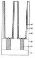
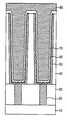
Translated fromKorean도 1a 내지 도 1e는 본 발명의 실시예에 따른 반도체 메모리 소자의 캐패시터 제조방법을 설명하기 위한 단면도.1A to 1E are cross-sectional views illustrating a method of manufacturing a capacitor of a semiconductor memory device according to an embodiment of the present invention.
※도면의 주요부분에 대한 부호의 설명※ Explanation of symbols for main parts of drawing
10 : 반도체 기판 20 : 층간절연막10
30 : 플러그 40 : 산화막30
50 : 하부전극 60 : 유전막50: lower electrode 60: dielectric film
70 : 상부전극 80 : 폴리실리콘막
70: upper electrode 80: polysilicon film
본 발명은 반도체 메모리 소자의 캐패시터 제조방법에 관한 것으로, 특히 방법에 관한 것으로, 특히 MPS(Metastable PolySilicon) 성장을 이용한 반도체 메모리 소자의 캐패시터 제조방법에 관한 것이다.BACKGROUND OF THE INVENTION 1. Field of the Invention The present invention relates to a method of manufacturing a capacitor of a semiconductor memory device, and more particularly, to a method of manufacturing a capacitor of a semiconductor memory device using metastable polysilicon (MPS) growth.
반도체 메모리 소자의 고집적화에 따라 캐패시터의 하부전극인 스토리지 노드전극의 형상을 대부분 내부 실린더형으로 형성하고 있다. 또한 좁은 셀면적 내에서 충분한 캐패시터를 확보하기 위하여, 하부전극 표면에 MPS를 성장시켜 표면적을 증가시키거나 유전막의 두께를 감소시키는 방법 등이 이루어지고 있다.As the semiconductor memory device is highly integrated, the shape of the storage node electrode, which is a lower electrode of the capacitor, is formed in an inner cylindrical shape. In addition, in order to secure sufficient capacitors within a narrow cell area, a method of increasing the surface area or decreasing the thickness of the dielectric film by growing MPS on the lower electrode surface has been made.
한편, 캐패시터에 MPS를 적용하는 경우, MPS의 형성 후 발생되는 자연산화막이나 열산화공정에 의한 열산화막으로 유전막을 형성하는데, 이러한 산화막은 MPS의 벌크보다 그레인 바운더리(grain boundary)에 먼저 형성되므로 MPS 표면에 불균일하게 형성되기 때문에, MPS와 산화막의 계면 거칠기(roughness) 특성을 저하시킨다. 이에 따라, 계면의 거친 부분에서 전계집중 현상이 발생하여 누설전류가 증가되고, 예컨대 유전막의 두께를 약 45Å까지만 형성할 수 있으므로, 디램(DRAM)과 같은 메모리 소자의 특성이 저하된다.
Meanwhile, when MPS is applied to a capacitor, a dielectric film is formed by a natural oxide film generated after the formation of the MPS or a thermal oxide film formed by a thermal oxidation process. Since it is formed nonuniformly on the surface, the interface roughness characteristic of MPS and an oxide film will fall. As a result, an electric field concentration phenomenon occurs at the rough portion of the interface to increase the leakage current, and for example, the thickness of the dielectric film can be formed up to about 45 mA, thereby degrading the characteristics of the memory device such as DRAM.
본 발명은 상기와 같은 종래기술의 문제점을 해결하기 위하여 제안된 것으로, MPS 표면에서 유전막이 균일하게 형성되도록 하여 MPS와 유전막의 계면 거칠기 특성을 향상시킴으로써 누설전류를 최소화하고 유전막 두께를 더욱더 감소시킬 수 있는 반도체 메모리 소자의 캐패시터 제조방법을 제공하는데 그 목적이 있다.
The present invention has been proposed to solve the above problems of the prior art, it is possible to minimize the leakage current and further reduce the dielectric film thickness by improving the interfacial roughness characteristics of the MPS and the dielectric film by uniformly forming the dielectric film on the MPS surface. It is an object of the present invention to provide a method for manufacturing a capacitor of a semiconductor memory device.
상기의 기술적 과제를 달성하기 위한 본 발명의 일 측면에 따르면, 상기의 본 발명의 목적은 상부에 층간절연막이 형성되어 있고, 층간절연막 내에 도전막의 플러그가 구비된 반도체 기판을 준비하는 단계; 상기 반도체기판 전면 상에 산화막을 형성하는 단계; 상기 플러그 및 플러그의 주변영역이 일부 노출되도록 산화막을 식각하여 캐패시터용 콘택홀을 형성하는 단계; 상기 콘택홀 및 산화막 표면 상에 제 1 폴리실리콘막을 증착하고 그 상부에 MPS를 성장시켜 하부전극을 형성하는 단계; 상기 하부전극을 산화막 표면이 노출되도록 전면 식각하여 상기 하부전극을 분리하는 단계; 상기 하부전극 표면 상에 발생된 자연산화막을 제거하는 단계; 상기 자연산화막이 제거된 하부전극 상부에 고밀도 플라즈마 방식으로 하부전극을 산화 또는 질화시켜 유전막을 형성하는 단계; 및 상기 유전막 상부에 금속막으로 이루어진 상부전극을 형성하는 단계를 포함하는 반도체 메모리 소자의 캐패시터 제조방법에 의해 달성될 수 있다.According to an aspect of the present invention for achieving the above technical problem, an object of the present invention comprises the steps of preparing a semiconductor substrate having an interlayer insulating film formed thereon, the conductive film is provided with a plug of the conductive film; Forming an oxide film on an entire surface of the semiconductor substrate; Etching the oxide layer to partially expose the plug and the peripheral area of the plug to form a contact hole for the capacitor; Depositing a first polysilicon layer on the contact hole and an oxide layer and growing MPS thereon to form a lower electrode; Separating the lower electrode by etching the entire lower electrode to expose an oxide film surface; Removing the native oxide film generated on the lower electrode surface; Forming a dielectric film by oxidizing or nitriding the lower electrode on the lower electrode from which the natural oxide film is removed by a high density plasma method; And forming an upper electrode formed of a metal film on the dielectric film.
바람직하게, 자연산화막은 HF 계열의 물질로 제거하고, 상기 고밀도 플라즈마 방식을 이용하여 유전막을 형성하는 단계는 NH3, O2, N2O, 또는 NO 개스를 이용하여 수행한다.Preferably, the natural oxide film is removed with an HF-based material, and the forming of the dielectric film using the high density plasma method is performed using NH3 , O2 , N2 O, or NO gas.
이하, 본 발명이 속한 기술분야에서 통상의 지식을 가진 자가 본 발명을 보다 용이하게 실시할 수 있도록 하기 위하여 본 발명의 바람직한 실시예를 소개하기로 한다.Hereinafter, preferred embodiments of the present invention will be introduced in order to enable those skilled in the art to more easily carry out the present invention.
도 1a 내지 도 1e는 본 발명의 실시예에 따른 반도체 메모리 소자의 캐패시터 제조방법을 설명하기 위한 단면도이다.1A to 1E are cross-sectional views illustrating a method of manufacturing a capacitor of a semiconductor memory device according to an embodiment of the present invention.
도 1a를 참조하면, 반도체 기판(10) 상에 층간절연막(20)을 형성한 후, 기판(10)의 일부가 노출되도록 층간절연막(20)을 식각하여 플러그용 제 1 콘택홀을 형성한다. 그 다음, 상기 제 1 콘택홀에 매립되도록 층간절연막(20) 상에 도전막 으로서 제 1 폴리실리콘막을 증착하고 층간절연막(20)의 표면이 노출되도록 전면 식각하여 폴리실리콘 플러그(30)를 형성한다. 즉, 이후 형성되는 캐패시터의 하부전극은 이 플러그(30)를 통하여 기판(10)의 활성영역과 콘택하게 된다.Referring to FIG. 1A, after forming the interlayer
그리고 나서, 기판의 전면 상부에 캐패시터 형성을 위한 산화막(40)을 증착하고, 포토리소그라피 및 식각공정을 이용하여 플러그(30) 및 이 플러그(30)의 주변영역이 일부 노출되도록 산화막(40)을 식각하여, 캐패시터용 제 2 콘택홀을 형성한다. 그 다음, 상기 제 2 콘택홀 및 산화막(40) 표면 상에 제 2 폴리실리콘막을 증착하고 그 상부에 MPS를 성장시켜, MPS에 의해 표면적이 향상된 내부 실린더형 하부전극(50)을 형성한다. 그 후, 하부전극(50)에 열적도핑을 실시하여 하부전극 (50)의 전기전도도를 향상시킨다.Then, an
도 1b를 참조하면, 하부전극(50)이 형성된 제 2 콘택홀에 매립되도록 기판 전면 상에 포토레지스트막(미도시)을 도포하고, 화학기계연마(Chemical Mechanical Polishing; CMP)을 이용하여 상기 포토레지스트막 및 하부전극(50)을 산화막(40)이 노출되도록 전면 식각하여 하부전극(50)을 서로 분리시킨다. 그 다음, 애이싱(ashing)을 이용하여 포토레지스트막을 제거하고, HF 계열의 물질로 하부전극(50)의 MPS 표면에 발생된 자연산화막 등을 제거한다.Referring to FIG. 1B, a photoresist film (not shown) is coated on the entire surface of the substrate so as to be buried in the second contact hole in which the
도 1c를 참조하면, 고밀도 플라즈마(High Density Plasma; HDP) 방식으로 하부전극(50) 표면을 산화 또는 질화시켜 하부전극(50) 표면 상에 유전막(60)을 형성한다. 바람직하게, HDP 방식은 NH3, O2, N2O, 또는 NO 개스를 이용하여 수행한다. 즉, HDP 방식은 플라즈마 내에 있는 이온(ion)과 라디칼(radical)이 플라즈마 포텐셜(plasma potential)로 방향성을 가지고 반응이 이루어지기 때문에, 유전막(60)이 MPS 표면에 균일하게 형성된다. 이에 따라, 하부전극(50)의 MPS와 유전막(60) 사이의 계면 거칠기 특성이 종래에 비해 향상됨으로써 누설전류를 최소화할 수 있을 뿐만 아니라, 유전막(60)을 35 내지 40Å 까지 얇게 형성하는 것도 가능하게 된다. 또한, HDP 방식을 이용한 산화 또는 질화공정시, 기판에 선택적으로 양전압(positive voltage)을 인가하여 산화 또는 질화과정을 증폭시킬 수도 있다.Referring to FIG. 1C, the
도 1d를 참조하면, 유전막(60) 상부에 TiN막과 같은 금속막을 증착하여 상부전극(70)을 형성하고, 도 1e에 도시된 바와 같이, 후속 열처리 공정시 캐패시터의 특성열화를 방지하기 위하여, 기판 전면 상에 제 3 폴리실리콘막(80)을 형성한다.Referring to FIG. 1D, the
상기 실시예에 의하면, 하부전극에 MPS 가 적용된 캐패시터의 제조시 유전막을 HDP 방식을 이용하여 형성함으로써, MPS 표면에 균일하게 유전막을 형성할 수 있게 되므로, 하부전극의 MPS와 유전막 사이의 계면 거칠기 특성이 종래에 비해 향상된다. 이에 따라, 누설전류가 최소화되어 디램과 같은 메모리 소자의 라이프타임(lift time)등이 길어질 뿐만 아니라, 유전막을 35 내지 40Å 까지 얇게 형성하는 것도 가능해져서, 메모리 소자의 특성을 향상시킬 수 있다.According to the above embodiment, since the dielectric film is formed by using the HDP method when manufacturing the capacitor to which the MPS is applied to the lower electrode, the dielectric film can be uniformly formed on the surface of the MPS. This is improved compared with the conventional one. As a result, the leakage current is minimized to increase the lift time of a memory device such as a DRAM, and to form a dielectric film as thin as 35 to 40 microseconds, thereby improving the characteristics of the memory device.
이상에서 설명한 본 발명은 전술한 실시예 및 첨부된 도면에 의해 한정되는 것이 아니고, 본 발명의 기술적 사상을 벗어나지 않는 범위 내에서 여러 가지 치환, 변형 및 변경이 가능하다는 것이 본 발명이 속하는 기술분야에서 통상의 지식을 가진 자에게 있어 명백할 것이다.
The present invention described above is not limited to the above-described embodiments and the accompanying drawings, and various substitutions, modifications, and changes are possible in the art without departing from the technical spirit of the present invention. It will be clear to those of ordinary knowledge.
전술한 본 발명은 MPS 표면에서 유전막이 균일하게 형성되도록 하여 MPS와 유전막의 계면 거칠기 특성을 향상시킴으로써 누설전류를 최소화하고 유전막 두께를 더욱더 감소시킬 수 있다.According to the present invention, the dielectric film is uniformly formed on the surface of the MPS, thereby improving the interfacial roughness characteristics of the MPS and the dielectric film, thereby minimizing leakage current and further reducing the dielectric film thickness.
Claims (8)
Translated fromKoreanPriority Applications (1)
| Application Number | Priority Date | Filing Date | Title |
|---|---|---|---|
| KR1020010084143AKR100799129B1 (en) | 2001-12-24 | 2001-12-24 | Capacitor Manufacturing Method of Semiconductor Memory Device |
Applications Claiming Priority (1)
| Application Number | Priority Date | Filing Date | Title |
|---|---|---|---|
| KR1020010084143AKR100799129B1 (en) | 2001-12-24 | 2001-12-24 | Capacitor Manufacturing Method of Semiconductor Memory Device |
Publications (2)
| Publication Number | Publication Date |
|---|---|
| KR20030054052A KR20030054052A (en) | 2003-07-02 |
| KR100799129B1true KR100799129B1 (en) | 2008-01-29 |
Family
ID=32212721
Family Applications (1)
| Application Number | Title | Priority Date | Filing Date |
|---|---|---|---|
| KR1020010084143AExpired - Fee RelatedKR100799129B1 (en) | 2001-12-24 | 2001-12-24 | Capacitor Manufacturing Method of Semiconductor Memory Device |
Country Status (1)
| Country | Link |
|---|---|
| KR (1) | KR100799129B1 (en) |
Cited By (9)
| Publication number | Priority date | Publication date | Assignee | Title |
|---|---|---|---|---|
| WO2013074369A1 (en)* | 2011-11-15 | 2013-05-23 | Applied Materials, Inc. | Method and apparatus for selective nitridation process |
| WO2018132252A1 (en)* | 2017-01-12 | 2018-07-19 | Micron Technology, Inc. | Memory cells and methods of forming a capacitor |
| US10553595B2 (en) | 2014-06-16 | 2020-02-04 | Micron Technology, Inc. | Memory cell and an array of memory cells |
| US10622556B2 (en) | 2015-07-24 | 2020-04-14 | Micron Technology, Inc. | Methods of forming an array of cross point memory cells |
| US10727336B2 (en) | 2014-04-24 | 2020-07-28 | Micron Technology, Inc. | Ferroelectric field effect transistors, pluralities of ferroelectric field effect transistors arrayed in row lines and column lines, and methods of forming a plurality of ferroelectric field effect transistors |
| US10741567B2 (en) | 2015-02-17 | 2020-08-11 | Micron Technology, Inc. | Memory cells |
| US10741755B2 (en) | 2015-07-24 | 2020-08-11 | Micron Technology, Inc. | Array of cross point memory cells |
| US10784374B2 (en) | 2014-10-07 | 2020-09-22 | Micron Technology, Inc. | Recessed transistors containing ferroelectric material |
| US11170834B2 (en) | 2019-07-10 | 2021-11-09 | Micron Technology, Inc. | Memory cells and methods of forming a capacitor including current leakage paths having different total resistances |
Families Citing this family (1)
| Publication number | Priority date | Publication date | Assignee | Title |
|---|---|---|---|---|
| KR101015089B1 (en)* | 2008-11-19 | 2011-02-16 | 라제건 | Cane with improved strap straps |
Citations (4)
| Publication number | Priority date | Publication date | Assignee | Title |
|---|---|---|---|---|
| KR20000027832A (en)* | 1998-10-29 | 2000-05-15 | 김영환 | Method for forming lower electrode of capacitors |
| KR20000039607A (en)* | 1998-12-15 | 2000-07-05 | 김영환 | Method for fabricating capacitor of semiconductor device |
| KR20010061016A (en)* | 1999-12-28 | 2001-07-07 | 박종섭 | Fabricating method for storage node of semiconductor device |
| KR20030003358A (en)* | 2001-06-30 | 2003-01-10 | 주식회사 하이닉스반도체 | Capacitor making methods of ferroelectric random access memory |
- 2001
- 2001-12-24KRKR1020010084143Apatent/KR100799129B1/ennot_activeExpired - Fee Related
Patent Citations (4)
| Publication number | Priority date | Publication date | Assignee | Title |
|---|---|---|---|---|
| KR20000027832A (en)* | 1998-10-29 | 2000-05-15 | 김영환 | Method for forming lower electrode of capacitors |
| KR20000039607A (en)* | 1998-12-15 | 2000-07-05 | 김영환 | Method for fabricating capacitor of semiconductor device |
| KR20010061016A (en)* | 1999-12-28 | 2001-07-07 | 박종섭 | Fabricating method for storage node of semiconductor device |
| KR20030003358A (en)* | 2001-06-30 | 2003-01-10 | 주식회사 하이닉스반도체 | Capacitor making methods of ferroelectric random access memory |
Cited By (14)
| Publication number | Priority date | Publication date | Assignee | Title |
|---|---|---|---|---|
| US8808564B2 (en) | 2011-11-15 | 2014-08-19 | Applied Materials, Inc. | Method and apparatus for selective nitridation process |
| WO2013074369A1 (en)* | 2011-11-15 | 2013-05-23 | Applied Materials, Inc. | Method and apparatus for selective nitridation process |
| US10727336B2 (en) | 2014-04-24 | 2020-07-28 | Micron Technology, Inc. | Ferroelectric field effect transistors, pluralities of ferroelectric field effect transistors arrayed in row lines and column lines, and methods of forming a plurality of ferroelectric field effect transistors |
| US10553595B2 (en) | 2014-06-16 | 2020-02-04 | Micron Technology, Inc. | Memory cell and an array of memory cells |
| US10784374B2 (en) | 2014-10-07 | 2020-09-22 | Micron Technology, Inc. | Recessed transistors containing ferroelectric material |
| US10741567B2 (en) | 2015-02-17 | 2020-08-11 | Micron Technology, Inc. | Memory cells |
| US11244951B2 (en) | 2015-02-17 | 2022-02-08 | Micron Technology, Inc. | Memory cells |
| US11706929B2 (en) | 2015-02-17 | 2023-07-18 | Micron Technology, Inc. | Memory cells |
| US10622556B2 (en) | 2015-07-24 | 2020-04-14 | Micron Technology, Inc. | Methods of forming an array of cross point memory cells |
| US10741755B2 (en) | 2015-07-24 | 2020-08-11 | Micron Technology, Inc. | Array of cross point memory cells |
| US10396145B2 (en) | 2017-01-12 | 2019-08-27 | Micron Technology, Inc. | Memory cells comprising ferroelectric material and including current leakage paths having different total resistances |
| WO2018132252A1 (en)* | 2017-01-12 | 2018-07-19 | Micron Technology, Inc. | Memory cells and methods of forming a capacitor |
| US11600691B2 (en) | 2017-01-12 | 2023-03-07 | Micron Technology, Inc. | Memory cells comprising ferroelectric material and including current leakage paths having different total resistances |
| US11170834B2 (en) | 2019-07-10 | 2021-11-09 | Micron Technology, Inc. | Memory cells and methods of forming a capacitor including current leakage paths having different total resistances |
Also Published As
| Publication number | Publication date |
|---|---|
| KR20030054052A (en) | 2003-07-02 |
Similar Documents
| Publication | Publication Date | Title |
|---|---|---|
| KR100401503B1 (en) | Method for fabricating capacitor of semiconductor device | |
| JP2000058779A (en) | Trench capacitor and method for forming the same | |
| KR100799129B1 (en) | Capacitor Manufacturing Method of Semiconductor Memory Device | |
| KR100825020B1 (en) | Capacitor Manufacturing Method of Semiconductor Memory Device | |
| US20070072388A1 (en) | Bottle-shaped trench and method of fabricating the same | |
| US6878601B1 (en) | Method for fabricating a capacitor containing metastable polysilicon | |
| KR100513808B1 (en) | Method for fabricating capacitor | |
| KR100543201B1 (en) | Capacitor Manufacturing Method of Semiconductor Memory Device | |
| KR20020096136A (en) | Method for manufacturing isolation of semiconductor device | |
| KR100445059B1 (en) | Method of fabricating capacitor of semiconductor device for improving physical property of capacitor bottom electrode | |
| KR100886704B1 (en) | How to Form Storage Node Electrode of Capacitor | |
| KR100520140B1 (en) | Method for forming capacitor of semiconductor device | |
| KR20010047999A (en) | Method For Fabricating Capacitor in Memory Cell | |
| KR20040059998A (en) | Method for manufacturing isolation layer in semiconductor device | |
| KR100517908B1 (en) | Semiconductor memory device and method for manufacturing the same | |
| KR100507364B1 (en) | Method for fabricating capacitor of semiconductor device | |
| KR20030000436A (en) | Method for manufacturing isolation of semiconductor device | |
| KR100361518B1 (en) | Method of fabricating a capacitor in a semiconductor device | |
| KR100290779B1 (en) | Method for forming charge storage electrode of DRAM device | |
| KR20020045266A (en) | Method for forming a dielectric of capacitor | |
| KR20030058817A (en) | A Capacitor of semiconductor device and method for fabricating the same | |
| KR20030025317A (en) | Method for fabricating capacitor of semiconductor device | |
| KR20010008406A (en) | Method for manufacturing charge storage electrode of capacitor | |
| KR20040008655A (en) | Method of manufacturing capacitor for semiconductor device | |
| KR19990060852A (en) | Capacitor Manufacturing Method of Semiconductor Device |
Legal Events
| Date | Code | Title | Description |
|---|---|---|---|
| PA0109 | Patent application | St.27 status event code:A-0-1-A10-A12-nap-PA0109 | |
| PG1501 | Laying open of application | St.27 status event code:A-1-1-Q10-Q12-nap-PG1501 | |
| A201 | Request for examination | ||
| PA0201 | Request for examination | St.27 status event code:A-1-2-D10-D11-exm-PA0201 | |
| D13-X000 | Search requested | St.27 status event code:A-1-2-D10-D13-srh-X000 | |
| D14-X000 | Search report completed | St.27 status event code:A-1-2-D10-D14-srh-X000 | |
| E902 | Notification of reason for refusal | ||
| PE0902 | Notice of grounds for rejection | St.27 status event code:A-1-2-D10-D21-exm-PE0902 | |
| P11-X000 | Amendment of application requested | St.27 status event code:A-2-2-P10-P11-nap-X000 | |
| P13-X000 | Application amended | St.27 status event code:A-2-2-P10-P13-nap-X000 | |
| E701 | Decision to grant or registration of patent right | ||
| PE0701 | Decision of registration | St.27 status event code:A-1-2-D10-D22-exm-PE0701 | |
| GRNT | Written decision to grant | ||
| PR0701 | Registration of establishment | St.27 status event code:A-2-4-F10-F11-exm-PR0701 | |
| PR1002 | Payment of registration fee | St.27 status event code:A-2-2-U10-U11-oth-PR1002 Fee payment year number:1 | |
| PG1601 | Publication of registration | St.27 status event code:A-4-4-Q10-Q13-nap-PG1601 | |
| G170 | Re-publication after modification of scope of protection [patent] | ||
| PG1701 | Publication of correction | St.27 status event code:A-5-5-P10-P19-oth-PG1701 Patent document republication publication date:20080414 Republication note text:Request for Correction Notice (Document Request) Gazette number:1007991290000 Gazette reference publication date:20080129 | |
| FPAY | Annual fee payment | Payment date:20101224 Year of fee payment:4 | |
| PR1001 | Payment of annual fee | St.27 status event code:A-4-4-U10-U11-oth-PR1001 Fee payment year number:4 | |
| LAPS | Lapse due to unpaid annual fee | ||
| PC1903 | Unpaid annual fee | St.27 status event code:A-4-4-U10-U13-oth-PC1903 Not in force date:20120124 Payment event data comment text:Termination Category : DEFAULT_OF_REGISTRATION_FEE | |
| PN2301 | Change of applicant | St.27 status event code:A-5-5-R10-R13-asn-PN2301 St.27 status event code:A-5-5-R10-R11-asn-PN2301 | |
| PC1903 | Unpaid annual fee | St.27 status event code:N-4-6-H10-H13-oth-PC1903 Ip right cessation event data comment text:Termination Category : DEFAULT_OF_REGISTRATION_FEE Not in force date:20120124 | |
| PN2301 | Change of applicant | St.27 status event code:A-5-5-R10-R13-asn-PN2301 St.27 status event code:A-5-5-R10-R11-asn-PN2301 | |
| PN2301 | Change of applicant | St.27 status event code:A-5-5-R10-R13-asn-PN2301 St.27 status event code:A-5-5-R10-R11-asn-PN2301 | |
| P22-X000 | Classification modified | St.27 status event code:A-4-4-P10-P22-nap-X000 | |
| P22-X000 | Classification modified | St.27 status event code:A-4-4-P10-P22-nap-X000 | |
| P22-X000 | Classification modified | St.27 status event code:A-4-4-P10-P22-nap-X000 |