KR100798350B1 - Self-reinforced plasma source with cross-arranged outer ferrite cores - Google Patents
Self-reinforced plasma source with cross-arranged outer ferrite coresDownload PDFInfo
- Publication number
- KR100798350B1 KR100798350B1KR1020060006199AKR20060006199AKR100798350B1KR 100798350 B1KR100798350 B1KR 100798350B1KR 1020060006199 AKR1020060006199 AKR 1020060006199AKR 20060006199 AKR20060006199 AKR 20060006199AKR 100798350 B1KR100798350 B1KR 100798350B1
- Authority
- KR
- South Korea
- Prior art keywords
- reaction chamber
- ferrite cores
- self
- plasma reaction
- plasma
- Prior art date
- Legal status (The legal status is an assumption and is not a legal conclusion. Google has not performed a legal analysis and makes no representation as to the accuracy of the status listed.)
- Expired - Fee Related
Links
Images


Classifications
- A—HUMAN NECESSITIES
- A61—MEDICAL OR VETERINARY SCIENCE; HYGIENE
- A61K—PREPARATIONS FOR MEDICAL, DENTAL OR TOILETRY PURPOSES
- A61K8/00—Cosmetics or similar toiletry preparations
- A61K8/02—Cosmetics or similar toiletry preparations characterised by special physical form
- A61K8/11—Encapsulated compositions
- A—HUMAN NECESSITIES
- A61—MEDICAL OR VETERINARY SCIENCE; HYGIENE
- A61K—PREPARATIONS FOR MEDICAL, DENTAL OR TOILETRY PURPOSES
- A61K8/00—Cosmetics or similar toiletry preparations
- A61K8/02—Cosmetics or similar toiletry preparations characterised by special physical form
- A61K8/0216—Solid or semisolid forms
- A61K8/0233—Distinct layers, e.g. core/shell sticks
- A—HUMAN NECESSITIES
- A61—MEDICAL OR VETERINARY SCIENCE; HYGIENE
- A61Q—SPECIFIC USE OF COSMETICS OR SIMILAR TOILETRY PREPARATIONS
- A61Q11/00—Preparations for care of the teeth, of the oral cavity or of dentures; Dentifrices, e.g. toothpastes; Mouth rinses
- A—HUMAN NECESSITIES
- A61—MEDICAL OR VETERINARY SCIENCE; HYGIENE
- A61K—PREPARATIONS FOR MEDICAL, DENTAL OR TOILETRY PURPOSES
- A61K2800/00—Properties of cosmetic compositions or active ingredients thereof or formulation aids used therein and process related aspects
- A61K2800/80—Process related aspects concerning the preparation of the cosmetic composition or the storage or application thereof
- A61K2800/92—Oral administration
Landscapes
- Health & Medical Sciences (AREA)
- Life Sciences & Earth Sciences (AREA)
- Animal Behavior & Ethology (AREA)
- General Health & Medical Sciences (AREA)
- Public Health (AREA)
- Veterinary Medicine (AREA)
- Birds (AREA)
- Epidemiology (AREA)
- Oral & Maxillofacial Surgery (AREA)
- Plasma Technology (AREA)
- Chemical Vapour Deposition (AREA)
- Drying Of Semiconductors (AREA)
Abstract
Translated fromKoreanDescription
Translated fromKorean본 발명의 상세한 설명에서 사용되는 도면을 보다 충분히 이해하기 위하여, 각 도면의 간단한 설명이 제공된다.In order to more fully understand the drawings used in the detailed description of the invention, a brief description of each drawing is provided.
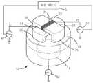
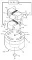
도 1은 본 발명의 제1 실시예에 따른 교차 배열된 페라이트 코어가 설치된 플라즈마 반응 챔버의 외관을 보여주는 사시도이다.1 is a perspective view showing the appearance of a plasma reaction chamber in which a ferrite core is arranged in a cross arrangement according to a first embodiment of the present invention.
도 2는 도 1의 플라즈마 반응 챔버의 내부 구조를 보여주는 단면도이다.FIG. 2 is a cross-sectional view illustrating an internal structure of the plasma reaction chamber of FIG. 1.
도 3a 및 도 3b는 교차 배열된 페라이트 코어의 유도 코일에 공급되는 주파수의 위상 변화를 설명하기 위한 파형도이다.3A and 3B are waveform diagrams for explaining the phase change of the frequency supplied to the induction coils of the ferrite cores arranged crosswise.
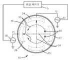
도 4는 교차 배열된 페라이트 코어의 자속 출입구의 형상과 플라즈마 반응 챔버 내부에서 이온의 가속 경로를 보여주는 도면이다.4 is a view showing the shape of the magnetic flux entrance and exit of the ferrite core cross-arranged and the acceleration path of the ions in the plasma reaction chamber.
도 5는 교차 배열된 페라이트 코어의 자속 출입구의 형상을 직각형 구조로 변형한 예를 보여주는 도면이다.5 is a view showing an example in which the shape of the magnetic flux entrance and exit of the ferrite cores arranged crosswise is modified into a rectangular structure.
도 6은 이중 바이어스 전원을 구비한 플라즈마 반응 챔버를 설명하기 위한 도면이다.6 is a view for explaining a plasma reaction chamber having a dual bias power supply.
도 7은 본 발명의 제2 실시예에 따른 교차 배열된 페라이트 코어가 설치된 플라즈마 반응 챔버의 외관을 보여주는 사시도이다.FIG. 7 is a perspective view showing the appearance of a plasma reaction chamber in which ferrite cores intersected with each other according to a second embodiment of the present invention are installed.
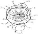
도 8은 도 7의 플라즈마 반응 챔버의 내부 천청 구조를 보여주기 위한 절개 사시도이다.FIG. 8 is a cutaway perspective view illustrating an internal celestial structure of the plasma reaction chamber of FIG. 7.
도 9는 자속 출구가 마주 대향하도록 절곡시킨 페라이트 코어를 채용한 변형예를 보여주는 사시도이다.9 is a perspective view showing a modification employing a ferrite core bent so that the magnetic flux outlets face each other.
도 10은 도 9의 프로세스 챔버의 내부 천정 구조를 보여주기 위한 절개 사시도이다.FIG. 10 is a cutaway perspective view illustrating an internal ceiling structure of the process chamber of FIG. 9.
도 11은 본 발명의 제3 실시예에 따른 교차 배열된 페라이트 코어가 설치된 플라즈마 반응 챔버의 외관을 보여주는 사시도이다.FIG. 11 is a perspective view showing an appearance of a plasma reaction chamber in which ferrite cores arranged in a cross according to a third embodiment of the present invention are installed.
도 12는 도 11의 플라즈마 반응 챔버의 내부 구조를 보여주는 단면도이다.12 is a cross-sectional view illustrating an internal structure of the plasma reaction chamber of FIG. 11.
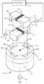
도 13은 플라즈마 반응 챔버의 상부 구조를 변형한 예를 보여주는 사시도이다. 그리고13 is a perspective view illustrating an example in which the upper structure of the plasma reaction chamber is modified. And
도 14는 도 13의 플라즈마 반응 챔버의 내부 천정 구조를 보여주기 위한 절개 사시도이다.FIG. 14 is a cutaway perspective view illustrating an internal ceiling structure of the plasma reaction chamber of FIG. 13.
*도면의 주요 부분에 대한 부호의 설명** Description of the symbols for the main parts of the drawings
10: 플라즈마 반응 챔버15: 서셉터10: plasma reaction chamber 15: susceptor
16: 샤워 헤드18: 기판16: shower head 18: substrate
20, 22: 페라이트 코어21, 23: 유도 코일20, 22:
30, 31, 32: 전원 공급원33: 플라즈마 이온 입자30, 31, 32: power supply 33: plasma ion particles
34: 평형 회전 이온 가속 경로34: Equilibrium Rotation Ion Acceleration Path
본 발명은 반도체 기판 처리를 위한 플라즈마 소오스에 관한 것으로, 구체적으로는 자기장을 이용하여 프로세스 챔버 내부의 플라즈마 밀도와 균일도를 강화시키는 자기 강화된 플라즈마 소오스에 관한 것이다.TECHNICAL FIELD The present invention relates to a plasma source for processing a semiconductor substrate, and more particularly, to a magnetically enhanced plasma source that uses a magnetic field to enhance plasma density and uniformity inside a process chamber.
반도체 소자의 초미세화와 그리고 기판 사이즈의 증가 그리고 새로운 처리 대상 물질 등장 등의 여러 요인으로 인하여 반도체 제조 공정에서는 더욱 향상된 기판 처리 기술이 요구되고 있다. 특히, 플라즈마를 이용한 반도체 제조 공정으로 건식 에칭 공정 분야나 물리적/화학적 기상 증착 분야에서는 이러한 기술적 요구에 대응하여 자기장을 이용하여 고밀도의 플라즈마를 균일하게 얻을 수 있는 플라즈마 소오스에 대한 기술 개발이 지속되고 있다.Due to various factors such as ultra miniaturization of semiconductor devices, increase in substrate size, and the emergence of new materials to be treated, further improvements in substrate processing technologies are required in the semiconductor manufacturing process. In particular, in the field of dry etching process and physical / chemical vapor deposition, semiconductor technology using plasma continues to develop technologies for plasma sources that can uniformly obtain high-density plasma using magnetic fields. .
일반적으로 플라즈마 반응관의 압력을 낮추면 이온의 평균자유거리가 늘어나 웨이퍼에 충돌하는 이온의 에너지가 증가하고 이온들의 간의 산란현상도 줄어들기 때문에 이방성 에칭에 유리한 것으로 알려져 있다. 그러나 압력이 낮아지면 전자들 역시 평균자유거리가 늘어나 중성원자들과의 충돌이 감소함으로 플라즈마 상태를 유지하기가 어려워진다. 그럼으로 낮은 압력에서도 플라즈마를 유지할 수 있도록 자기장을 이용하여 전자들의 이동 거리를 증가시켜 중성원자들과의 충돌 빈도를 높여 낮은 압력에서도 플라즈마가 유지될 수 있는 기술이 제안되고 있다.In general, lowering the pressure of the plasma reaction tube increases the average free distance of ions, which increases the energy of ions colliding with the wafer and reduces scattering between the ions, which is known to be advantageous for anisotropic etching. However, when the pressure is lowered, the electrons also increase the average free distance, which reduces the collision with neutral atoms, making it difficult to maintain the plasma state. Therefore, a technique has been proposed to maintain the plasma at low pressure by increasing the frequency of collision with the neutral atoms by increasing the moving distance of electrons by using the magnetic field to maintain the plasma at low pressure.
또한, 기판 사이즈의 증가에 따라 기판이 처리되는 플라즈마 반응 챔버의 사 이즈도 증가되는데 이러한 경우 플라즈마 반응 챔버의 내부에 균일하게 플라즈마가 분포하기 어렵다. 그럼으로 자기장을 이용하여 플라즈마 반응 챔버의 내부에서 균일한 플라즈마 밀도가 유지될 수 있도록 하는 기술들이 제안되고 있다.In addition, as the substrate size increases, the size of the plasma reaction chamber in which the substrate is processed also increases. In this case, it is difficult to uniformly distribute the plasma inside the plasma reaction chamber. Therefore, techniques for using a magnetic field to maintain a uniform plasma density inside the plasma reaction chamber have been proposed.
플라즈마 반응 챔버의 내부에 균일한 플라즈마가 형성되도록 하기 위하여 영구 자석을 이용한 기술들이 제안되고 있다. 예를 들어, 영구 자석을 반응관 상부에 장착하거나, 상부에서 회전 시키는 등의 기술들이 제안되어 있다. 또는 기판을 회전 시켜서 비교적 균일한 기판 처리가 될 수 있도록 하고도 있다.Techniques using permanent magnets have been proposed to form a uniform plasma inside the plasma reaction chamber. For example, techniques have been proposed, such as mounting a permanent magnet on top of a reaction tube, or rotating on top. Alternatively, the substrate may be rotated to allow a relatively uniform substrate treatment.
영구 자석을 이용한 경우에는 크기가 작고 장착이 간단하며 별도로 외부에서 전원을 공급하지 않아도 되기 때문에 비교적 간단히 균일도를 향상 시킬 수는 있다. 그러나 자기장의 균일도가 좋지 않으며 자기장의 세기도 제어가 불가능하다. 기판을 회전하거나 영구 자석을 회전하는 경우에는 회전 구조물을 구성하기 위한 부담이 있다.In the case of using permanent magnets, the uniformity can be improved relatively simply because they are small in size, simple to install, and do not require external power supply. However, the uniformity of the magnetic field is not good and the strength of the magnetic field is not controllable. When rotating a substrate or rotating a permanent magnet, there exists a burden for constructing a rotating structure.
따라서 본 발명은 플라즈마 반응 챔버 내부에 고밀도의 플라즈마를 보다 균일하게 발생 유지할 수 있도록 반응 챔버의 내부에 평형 회전 이온 가속 경로를 유도하도록 교차 배열된 외부 페라이트 코어를 구비한 자기 강화된 플라즈마 소오스를 제공하는데 그 목적이 있다.Accordingly, the present invention provides a self-reinforced plasma source having an external ferrite core cross-arranged to induce an equilibrium rotational ion acceleration path inside the reaction chamber to more uniformly generate and maintain a high density plasma inside the plasma reaction chamber. The purpose is.
상기한 기술적 과제를 달성하기 위한 본 발명의 일면은 교차 배열된 외부 페라이트 코어를 구비한 자기 강화된 플라즈마 소오스에 관한 것이다. 본 발명의 플라즈마 소오스는: 기판이 놓이는 서셉터가 내부에 구비된 플라즈마 반응 챔버; 자속 출입구가 플라즈마 반응 챔버의 내측으로 향하여 플라즈마 반응 챔버의 내측으로 자속이 출력되도록 하며, 상하로 이격되어 플라즈마 반응 챔버의 상부를 가로질러 교차 배열된 제1 및 제2 페라이트 코어; 제1 및 제2 페라이트 코어에 각각 감겨 제1 및 제2 페라이트 코어에 자기장을 유도 시키는 제1 및 제2 유도 코일; 제1 유도 코일로 제1 주파수의 전원을 공급하는 제1 전원 공급원; 제2 유도 코일로 제2 주파수의 전원을 공급하는 제2 전원 공급원; 및 제1 및 제2 전원 공급원의 주파수의 위상차를 제어하여 제1 및 제2 페라이트 코어에 의해 유도되는 자기장의 벡터적 합에 의해 기판 상부에 평형 회전 이온 가속 경로가 유도 되도록 한다.One aspect of the present invention for achieving the above technical problem relates to a self-enhanced plasma source having a cross-arranged outer ferrite core. The plasma source of the present invention comprises: a plasma reaction chamber having a susceptor on which a substrate is placed; First and second ferrite cores arranged to cross the upper portion of the plasma reaction chamber so that magnetic flux is output to the inside of the plasma reaction chamber toward the inside of the plasma reaction chamber; First and second induction coils wound around the first and second ferrite cores to induce a magnetic field in the first and second ferrite cores, respectively; A first power supply for supplying power at a first frequency to the first induction coil; A second power supply for supplying power at a second frequency to the second induction coil; And controlling the phase difference of the frequencies of the first and second power sources so that a balanced rotational ion acceleration path is induced on the substrate by the vector sum of the magnetic fields induced by the first and second ferrite cores.
이 실시예에 있어서, 제1 및 제2 페라이트 코어의 자속 출입구가 접하는 플라즈마 반응 챔버의 상부는 절연체로 구성된다.In this embodiment, the upper portion of the plasma reaction chamber that the magnetic flux entrance and exit of the first and second ferrite cores contact is made of an insulator.
이 실시예에 있어서, 제1 및 제2 페라이트 코어는 직각으로 교차 배열된다.In this embodiment, the first and second ferrite cores are intersected at right angles.
이 실시예에 있어서, 서셉터로 제3 주파수를 갖는 제1 바이어스 전원을 공급하는 제3 전원 공급원을 포함한다.In this embodiment, a third power supply for supplying a first bias power source having a third frequency to the susceptor is included.
이 실시예에 있어서, 서셉터로 제3 주파수를 갖는 제1 바이어스 전원을 공급하는 제3 전원 공급원과 제4 주파수를 갖는 제2 바이어스 전원을 공급하는 제4 전원 공급원을 포함한다.In this embodiment, a third power supply for supplying a first bias power source having a third frequency to the susceptor and a fourth power supply source for supplying a second bias power source having a fourth frequency are included.
이 실시예에 있어서, 플라즈마 반응 챔버는 상부 중심으로 구비된 가스 입구와 가스 입구로 유입된 가스가 서셉터를 향하여 고르게 분사되어 흐르도록 하는 샤 워 헤드를 구비한다.In this embodiment, the plasma reaction chamber has a gas inlet provided as an upper center and a shower head to allow the gas introduced into the gas inlet to flow evenly toward the susceptor.
이 실시예에 있어서, 제1 및 제2 페라이트 코어의 자속 출입구는 샤워 헤드의 외측으로 정렬된다.In this embodiment, the magnetic flux entrances of the first and second ferrite cores are aligned to the outside of the shower head.
이 실시예에 있어서, 제1 및 제2 페라이트 코어는 자속 출입구의 단면은 직사각형 구조 또는 호(arc) 구조 중 어느 하나의 구조를 갖는다.In this embodiment, the cross sections of the magnetic flux entrance and exit of the first and second ferrite cores have either a rectangular structure or an arc structure.
본 발명의 다른 특징에 따른 플라즈마 소오스는: 기판이 놓이는 서셉터가 내부에 구비된 플라즈마 반응 챔버; 플라즈마 반응 챔버의 상부에 형성되며 마주 대향하여 쌍을 이루는 제1 및 제2 코어 삽입구; 제1 및 제2 코어 삽입구에 양단의 자속 출입구가 삽입되어 플라즈마 반응 챔버의 내측으로 자속이 출력되도록 하며, 상하로 이격되어 플라즈마 반응 챔버의 상부를 가로질러 교차 배열되는 제1 및 제2 페라이트 코어; 제1 및 제2 페라이트 코어에 각각 감겨 제1 및 제2 페라이트 코어에 자기장을 유도 시키는 제1 및 제2 유도 코일; 제1 유도 코일로 제1 주파수의 전원을 공급하는 제1 전원 공급원; 제2 유도 코일로 제2 주파수의 전원을 공급하는 제2 전원 공급원; 및 제1 및 제2 전원 공급원의 주파수의 위상차를 제어하여 제1 및 제2 페라이트 코어에 의해 유도되는 자기장의 벡터적 합에 의해 기판 상부에 평형 회전 이온 가속 경로가 유도 된다.According to another aspect of the present invention, a plasma source includes: a plasma reaction chamber having a susceptor on which a substrate is placed; First and second core insertion holes formed on an upper portion of the plasma reaction chamber and paired to face each other; First and second ferrite cores having magnetic flux output to the inside of the plasma reaction chamber by inserting magnetic flux entrances at both ends into the first and second core insertion holes, and spaced vertically and intersecting the upper portion of the plasma reaction chamber; First and second induction coils wound around the first and second ferrite cores to induce a magnetic field in the first and second ferrite cores, respectively; A first power supply for supplying power at a first frequency to the first induction coil; A second power supply for supplying power at a second frequency to the second induction coil; And controlling the phase difference between the frequencies of the first and second power sources to induce a balanced rotational ion acceleration path over the substrate by the vector sum of the magnetic fields induced by the first and second ferrite cores.
이 실시예에 있어서, 제1 및 제2 페라이트 코어의 자속 출입구가 접하는 플라즈마 반응 챔버의 상부는 절연체로 구성된다.In this embodiment, the upper portion of the plasma reaction chamber that the magnetic flux entrance and exit of the first and second ferrite cores contact is made of an insulator.
이 실시예에 있어서, 제1 및 제2 페라이트 코어는 직각으로 교차 배열된다.In this embodiment, the first and second ferrite cores are intersected at right angles.
이 실시예에 있어서, 서셉터로 제3 주파수를 갖는 제1 바이어스 전원을 공급 하는 제3 전원 공급원을 포함한다.In this embodiment, a third power supply for supplying a first bias power source having a third frequency to the susceptor is included.
이 실시예에 있어서, 서셉터로 제3 주파수를 갖는 제1 바이어스 전원을 공급하는 제3 전원 공급원과 제4 주파수를 갖는 제2 바이어스 전원을 공급하는 제4 전원 공급원을 포함한다.In this embodiment, a third power supply for supplying a first bias power source having a third frequency to the susceptor and a fourth power supply source for supplying a second bias power source having a fourth frequency are included.
이 실시예에 있어서, 플라즈마 반응 챔버는 상부 중심으로 구비된 가스 입구와 가스 입구로 유입된 가스가 서셉터를 향하여 고르게 분사되어 흐르도록 하는 샤워 헤드를 구비한다.In this embodiment, the plasma reaction chamber includes a gas inlet provided as an upper center and a shower head to allow the gas introduced into the gas inlet to flow evenly toward the susceptor.
이 실시예에 있어서, 제1 및 제2 코어 삽입구는 샤워 헤드의 외측으로 정렬된다.In this embodiment, the first and second core inserts are aligned out of the shower head.
이 실시예에 있어서, 제1 및 제2 페라이트 코어와 제1 및 제2 코어 삽입구는 각기 직사각형 구조 또는 호(arc) 구조 중 어느 하나의 구조를 갖는다.In this embodiment, the first and second ferrite cores and the first and second core insertion holes each have either a rectangular structure or an arc structure.
이 실시예에 있어서, 제1 및 제2 페라이트 코어는 자속 출입구가 마주 대향하도록 절곡된 구조를 갖고, 이에 적합하게 제1 및 제2 코어 삽구도 끝단이 절곡된 구조를 갖는다.In this embodiment, the first and second ferrite cores have a structure bent such that the magnetic flux entrances face each other, and suitably the ends of the first and second core inserts are also bent.
본 발명의 또 다른 특징에 따른 플라즈마 소오스는: 기판이 놓이는 서셉터가 내부에 구비된 플라즈마 반응 챔버; 자속 출입구가 플라즈마 반응 챔버의 외측 상단 측벽으로 배치되어 자속 출입구가 마주 대향하고 플라즈마 반응 챔버의 내측으로 자속이 출력되도록 하며, 상하로 이격되어 플라즈마 반응 챔버의 상부를 가로질러 교차 배열된 제1 및 제2 페라이트 코어; 제1 및 제2 페라이트 코어에 각각 감겨 제1 및 제2 페라이트 코어에 자기장을 유도 시키는 제1 및 제2 유도 코일; 제1 유도 코일로 제1 주파수의 전원을 공급하는 제1 전원 공급원; 제2 유도 코일로 제2 주파수의 전원을 공급하는 제2 전원 공급원; 및 제1 및 제2 전원 공급원의 주파수의 위상차를 제어하여 제1 및 제2 페라이트 코어에 의해 유도되는 자기장의 벡터적 합에 의해 기판 상부에 평형 회전 이온 가속 경로가 유도 되도록 한다.According to another aspect of the present invention, a plasma source includes: a plasma reaction chamber having a susceptor on which a substrate is placed; First and second magnetic flux entrances are arranged on the outer top sidewall of the plasma reaction chamber so that the magnetic flux entrances face each other and the magnetic flux is output to the inside of the plasma reaction chamber, and spaced vertically and intersected across the top of the plasma reaction chamber. 2 ferrite cores; First and second induction coils wound around the first and second ferrite cores to induce a magnetic field in the first and second ferrite cores, respectively; A first power supply for supplying power at a first frequency to the first induction coil; A second power supply for supplying power at a second frequency to the second induction coil; And controlling the phase difference of the frequencies of the first and second power sources so that a balanced rotational ion acceleration path is induced on the substrate by the vector sum of the magnetic fields induced by the first and second ferrite cores.
이 실시예에 있어서, 제1 및 제2 페라이트 코어의 자속 출입구가 접하는 플라즈마 반응 챔버의 측벽면은 절연체로 구성된다.In this embodiment, the side wall surface of the plasma reaction chamber that the magnetic flux entrance and exit of the first and second ferrite cores contact is made of an insulator.
이 실시예에 있어서, 제1 및 제2 페라이트 코어는 직각으로 교차 배열된다.In this embodiment, the first and second ferrite cores are intersected at right angles.
이 실시예에 있어서, 서셉터로 제3 주파수를 갖는 제1 바이어스 전원을 공급하는 제3 전원 공급원을 포함한다.In this embodiment, a third power supply for supplying a first bias power source having a third frequency to the susceptor is included.
이 실시예에 있어서, 서셉터로 제3 주파수를 갖는 제1 바이어스 전원을 공급하는 제3 전원 공급원과 제4 주파수를 갖는 제2 바이어스 전원을 공급하는 제4 전원 공급원을 포함한다.In this embodiment, a third power supply for supplying a first bias power source having a third frequency to the susceptor and a fourth power supply source for supplying a second bias power source having a fourth frequency are included.
이 실시예에 있어서, 플라즈마 반응 챔버는 상부 중심으로 구비된 가스 입구와 가스 입구로 유입된 가스가 서셉터를 향하여 고르게 분사되어 흐르도록 플라즈마 반응 챔버의 천정에 구비되는 샤워 헤드를 포함한다.In this embodiment, the plasma reaction chamber includes a gas inlet provided as an upper center and a shower head provided on the ceiling of the plasma reaction chamber so that the gas introduced into the gas inlet flows evenly toward the susceptor.
이 실시예에 있어서, 플라즈마 반응 챔버는 상부가 테두리를 따라 하나의 계단형으로 구성되어 천정의 중심이 융기된 영역을 구비하고, 융기된 영역의 내측 천정에 샤워 헤드가 구비되며, 융기된 영역의 외부 측벽으로 제1 및 제2 페라이트 코어의 자속 출입구가 접한다.In this embodiment, the plasma reaction chamber has a stepped top along the rim of the plasma reaction chamber, the center of the ceiling having a raised area, the shower head is provided on the inner ceiling of the raised area, The outer sidewall abuts the magnetic flux entrances of the first and second ferrite cores.
이 실시예에 있어서, 제1 및 제2 페라이트 코어의 자속 출입구는 샤워 헤드의 하단으로 정렬된다.In this embodiment, the magnetic flux entrances of the first and second ferrite cores are aligned with the bottom of the shower head.
이 실시예에 있어서, 제1 및 제2 페라이트 코어는 자속 출입구의 단면은 직사각형 구조 또는 호(arc) 구조 중 어느 하나의 구조를 갖는다.In this embodiment, the cross sections of the magnetic flux entrance and exit of the first and second ferrite cores have either a rectangular structure or an arc structure.
본 발명과 본 발명의 동작상의 이점 및 본 발명의 실시예에 의하여 달성되는 목적을 충분히 이해하기 위해서는 본 발명의 바람직한 실시예를 예시하는 첨부 도면 및 첨부 도면에 기재된 내용을 참조하여야 한다. 각 도면을 이해함에 있어서, 동일한 부재는 가능한 한 동일한 참조부호로 도시하고자 함에 유의하여야 한다. 그리고 본 발명의 요지를 불필요하게 흐릴 수 있다고 판단되는 공지 기능 및 구성에 대한 상세한 기술은 생략된다.DETAILED DESCRIPTION In order to fully understand the present invention, the operational advantages of the present invention, and the objects achieved by the embodiments of the present invention, reference should be made to the accompanying drawings which illustrate preferred embodiments of the present invention and the contents described in the accompanying drawings. In understanding the drawings, it should be noted that like parts are intended to be represented by the same reference numerals as much as possible. And detailed description of known functions and configurations that are determined to unnecessarily obscure the subject matter of the present invention is omitted.
이하, 첨부된 도면을 참조하여 본 발명의 바람직한 실시예를 설명함으로써, 본 발명의 교차 배열된 외부 페라이트 코어를 구비한 자기 강화된 플라즈마 소오스를 상세히 설명한다.DESCRIPTION OF THE PREFERRED EMBODIMENTS Hereinafter, a self-enhanced plasma source having a cross-arranged outer ferrite core of the present invention will be described in detail with reference to the accompanying drawings.
(제1 실시예)(First embodiment)
도 1은 본 발명의 제1 실시예에 따른 교차 배열된 페라이트 코어가 설치된 플라즈마 반응 챔버의 외관을 보여주는 사시도이고, 도 2는 도 1의 플라즈마 반응 챔버의 내부 구조를 보여주는 단면도이다.1 is a perspective view showing the appearance of a plasma reaction chamber having a cross-ferred ferrite core according to a first embodiment of the present invention, Figure 2 is a cross-sectional view showing the internal structure of the plasma reaction chamber of FIG.
도 1 및 도 2를 참조하여, 본 발명의 제1 실시예에 따른 플라즈마 반응 챔버(10)는 내부(19)에 기판(18)이 놓이는 서셉터(15)가 구비된다. 플라즈마 반응 챔버(10)의 상부(13)에는 제1 및 제2 페라이트 코어(20, 22)가 설치된다. 제1 및 제2 페라이트 코어(20, 22)는 각각의 자속 출입구(24, 25)(26, 27)가 플라즈마 반응 챔버(10)의 내측으로 향하도록 설치되어 플라즈마 반응 챔버(10)의 내측으로 자속이 출력되도록 한다. 그리고 제1 및 제2 페라이트 코어(20, 22)는 상하로 이격되어 플라즈마 반응 챔버(10)의 상부를 가로질러 교차 배열된다. 바람직하게는 제1 및 제2 페라이트 코어(20, 22)는 직각으로 교차 배열된다.1 and 2, the
그럼으로, 도 4에 도시된 바와 같이, 제1 및 제2 페라이트 코어(20, 22) 자속 출입구(24, 25)(26, 27)로부터 출력되는 자속(34)은 플라즈마 반응 챔버(10)의 내부(19)에서 상호 직교하게 된다. 제1 및 제2 페라이트 코어(20, 22)의 자속 출입구(24, 25)(26, 27)가 접하는 플라즈마 반응 챔버(10)의 상부(13)는 절연체로 구성되는 것이 바람직하다. 제1 및 제2 페라이트 코어(20, 22)는 자속 출입구(24, 25)(26, 27)의 단면이 호(arc) 구조를 가도록 하여 전체적으로 원형 구조를 가도록 하지만, 도 5에 도시된 바와 같이, 직사각형 구조를 갖도록 할 수 있으며 후술되는 제2 및 제3 실시예서도 동일하게 적용된다.Thus, as shown in FIG. 4, the
제1 및 제2 페라이트 코어(20, 22)에는 각기 제1 및 제2 유도 코일(21, 23)이 감겨 제1 및 제2 페라이트 코어(21, 23)에 자기장을 유도 시킨다. 제1 유도 코일(21)은 제1 전원 공급원(30)에 전기적으로 연결되어 제1 주파수(f1)의 전원을 공급받는다. 제2 유도 코일(23)은 제2 전원 공급원(31)에 전기적으로 연결되어 제2 주파수(f2)의 전원을 공급받는다.The first and
제1 및 제2 전원 공급원(30, 31)은 위상 제어기(5)에 연결된다. 위상 제어 기(5)는 첨부 도면 도 3a 및 도 3b에 도시된 바와 같이 제1 및 제2 전원 공급원(30, 31)의 주파수(f1, f2) 위상을 제어하여 두 주파수의 위상차가 180도에서 90도 까지 차이가 나도록 제어한다. 초기 플라즈마 방전시에는 180도의 위상차를 갖도록 하는 것이 바람직하고, 플라즈마 방전 이후에는 90도의 위상차를 갖도록 하는 것이 바람직하다. 그럼으로 도 4에 도시된 바와 같이, 제1 및 제2 페라이트 코어(20, 22)에 의해 유도되는 자기장(34)의 벡터적 합에 의해 기판(18) 상부에 평형 회전 이온 가속 경로가 유도된다. 플라즈마 이온 입자(33)들은 이 경로를 따라 가속하게 된다. 그럼으로 플라즈마 반응 챔버(10)의 내부(19)에 고밀도의 플라즈마를 보다 균일하게 발생 유지할 수 있다.The first and
다시 도 2를 참조하여, 플라즈마 반응 챔버(10)는 상부 중심으로 가스 입구(17)가 구비되며, 가스 입구(17)로 유입된 가스가 서셉터(15)를 향하여 고르게 분사되어 흐르도록 하는 샤워 헤드(16)가 구비된다. 그리고 제1 및 제2 페라이트 코어(20, 22)의 자속 출입구(24, 25)(26, 27)는 샤워 헤드(16)의 외측으로 정렬되는 것이 바람직하다.Referring back to FIG. 2, the
제1 및 제2 주파수(f1, f2)는 동일한 주파수를 갖도록 하는 것이 바람직하며, 대략 10KHz ~ 100MHz의 범위에서 주파수를 선택할 수 있다. 서셉터(15)에는 제3 주파수의 바이어스 전원(32)이 연결된다. 제3 주파수는 일반적인 13.56MHz 주파수를 사용할 수 있으나 그보다 높은 혹은 낮은 주파수의 사용도 가능하다.Preferably, the first and second frequencies f1 and f2 have the same frequency, and a frequency can be selected within a range of approximately 10 KHz to 100 MHz. The
또한, 도 6에 도시된 바와 같이, 두 개의 바이어스 전원(32)(36)을 사용한 이중 전원 구조를 갖도록 할 수 있다. 서셉터로 제3 주파수를 갖는 제1 바이어스 전원을 공급하는 제3 전원 공급원(32)과 제4 주파수를 갖는 제2 바이어스 전원을 공급하는 제4 전원 공급원(36)이 구성된다. 제1 바이어스 전원의 제3 주파수는 일반적인 13.56MHz의 주파수를 사용할 수 있으나 그 보다 높은 혹은 낮은 주파수의 사용도 가능하다. 제2 바이어스 전원의 제4 주파수는 플라즈마 이온 입자가 기판(15)으로 가속되는 것을 제어하기 위한 것이다. 이러한 단일 또는 이중 바이어스 구조는 후술되는 제2 및 제3 실시예에서도 동일하게 적용된다.In addition, as shown in FIG. 6, it is possible to have a dual power supply structure using two
이상과 같은 본 발명의 제1 실시예에 따른 자기 강화된 플라즈마 소오스는 반응 챔버의 상부에 수직으로 교차 배열되는 두 개의 제1 및 제2 페라이트 코어(20, 22)에 의해서 반응 챔버의 내측 기판의 상부에 평형 회전 이온 가속 경로가 유됨으로서 플라즈마 반응 챔버 내부에 고밀도의 플라즈마를 보다 균일하게 발생하고 유지된다. 그럼으로 목적으로 하는 기판 가공을 보다 정밀하고 균일하게 미세 가공할 수 있다.The self-reinforced plasma source according to the first embodiment of the present invention as described above has two first and
(제2 실시예)(2nd Example)
계속해서, 첨부 도면 도 7 내지 도 10을 참조하여 본 발명의 제2 실시예에 따른 교차 배열된 외부 페라이트 코어를 구비한 자기 강화된 플라즈마 소오스를 설명한다. 제2 실시예의 설명에 있어서 상술한 제1 실시예와 동일한 구성에 대해서는 반복된 설명을 생략한다.Subsequently, with reference to the accompanying drawings, FIGS. 7 to 10, a self-strengthened plasma source having a cross-arranged outer ferrite core according to a second embodiment of the present invention will be described. In the description of the second embodiment, the repeated description of the same configuration as that of the first embodiment described above will be omitted.
도 7은 본 발명의 제2 실시예에 따른 교차 배열된 페라이트 코어가 설치된 플라즈마 반응 챔버의 외관을 보여주는 사시도이고, 도 8은 도 7의 플라즈마 반응 챔버의 내부 천청 구조를 보여주기 위한 절개 사시도이다.FIG. 7 is a perspective view illustrating an external appearance of a plasma reaction chamber in which ferrite cores intersected with each other according to a second embodiment of the present invention are installed, and FIG. 8 is a cutaway perspective view illustrating an internal ceiling structure of the plasma reaction chamber of FIG. 7.
도 7 및 도 8을 참조하여, 본 발명의 제2 실시예에 따른 플라즈마 반응 챔버(10a)는 상부(13a)에 마주 대향하여 쌍을 이루는 제1 및 제2 코어 삽입구(40, 41)(42, 43)가 형성된다. 제1 및 제2 코어 삽입구(40, 41)(42, 43)에는 제1 및 제2 페라이트 코어(20, 22)의 자속 출입구(24, 25)(26, 27)가 삽입되어 장착된다. 제1 및 제2 페라이트 코어(20, 22)의 자속 출입구(24, 25)(26, 27)가 접하는 플라즈마 반응 챔버(10a)의 상부(13a)는 절연체로 구성된다. 제1 및 제2 페라이트 코어(20, 22)는 상술한 제1 실시예와 동일한 구조로 직각 교차 배열된다.Referring to FIGS. 7 and 8, the
플라즈마 반응 챔버(10a)는 상부 중심으로 구비된 가스 입구(17)와 가스 입구(17)로 유입된 가스가 서셉터(15)를 향하여 고르게 분사되어 흐르도록 하는 샤워 헤드(16)를 구비한다. 제1 및 제2 코어 삽입구(40, 41)(42, 43)는 샤워 헤드(16)의 외측으로 정렬된다.The
도 9는 자속 출구가 마주 대향하도록 절곡시킨 페라이트 코어를 채용한 변형예를 보여주는 사시도이고, 도 10은 도 9의 프로세스 챔버의 내부 천정 구조를 보여주기 위한 절개 사시도이다.FIG. 9 is a perspective view showing a modified example employing a ferrite core bent so that the magnetic flux outlets face each other, and FIG. 10 is a cutaway perspective view illustrating the internal ceiling structure of the process chamber of FIG. 9.
도 9 및 도 10을 참조하여, 변형예에 따른 제1 및 제2 페라이트 코어(20a, 22a)는 자속 출입구(24a, 25a)(26a, 27a)가 마주 대향하도록 절곡된 구조를 갖는다. 그리고 이에 적합하게 제1 및 제 코어 삽입구(40a, 41a)(42a, 43a)도 끝단이 절곡된 구조를 갖는다.9 and 10, the first and
본 발명의 제2 실시예에 따른 플라즈마 반응 챔버(10a)는 제1 및 제2 페라이 트 코어(20, 22)에 의한 자기장이 좀 더 낮게 플라즈마 반응 챔버(10a)의 내부에 형성됨으로 기판 처리 효율을 보다 향상 시킬 수 있다.The
(제3 실시예)(Third Embodiment)
계속해서, 첨부 도면 도 11 내지 도 14를 참조하여 본 발명의 제3 실시예에 따른 교차 배열된 외부 페라이트 코어를 구비한 자기 강화된 플라즈마 소오스를 설명한다. 제3 실시예의 설명에 있어서 상술한 제1 및 제2 실시예와 동일한 구성에 대해서는 반복된 설명을 생략한다.Subsequently, with reference to the accompanying drawings, FIGS. 11 to 14, a self-enhanced plasma source having a cross-arranged outer ferrite core according to a third embodiment of the present invention will be described. In the description of the third embodiment, the repeated description of the same configuration as that of the first and second embodiments described above is omitted.
도 11은 본 발명의 제3 실시예에 따른 교차 배열된 페라이트 코어가 설치된 플라즈마 반응 챔버의 외관을 보여주는 사시도이고, 도 12는 도 11의 플라즈마 반응 챔버의 내부 구조를 보여주는 단면도이다.FIG. 11 is a perspective view illustrating an external appearance of a plasma reaction chamber having cross ferrite cores arranged in accordance with a third embodiment of the present invention, and FIG. 12 is a cross-sectional view illustrating an internal structure of the plasma reaction chamber of FIG.
도 11 및 도 12를 참조하여, 본 발명의 제3 실시예에 따른 플라즈마 반응 챔버(10b)는 제1 및 제2 페라이트 코어(20b, 22b)의 자속 출입구(24b, 25b)(26b, 27b)가 플라즈마 반응 챔버(10b)의 외측 상단 측벽(12)으로 배치되어 마주 대향한다. 그리하여 플라즈마 반응 챔버(10b)의 내측으로 자속이 출력되도록 하며, 제1 및 제2 페라이트 코어(20b, 22b)는 상하로 이격되어 플라즈마 반응 챔버의 상부를 가로질러 직각으로 교차 배열된다. 제1 및 제2 페라이트 코어(20b, 22b)의 자속 출입구(24b, 25b)(26b, 27b)가 접하는 플라즈마 반응 챔버(10b)의 측벽면(12)은 절연체로 구성된다.11 and 12, the
플라즈마 반응 챔버(10b)는 상부 중심으로 구비된 가스 입구(17)와 가스 입구로 유입된 가스가 서셉터(15)를 향하여 고르게 분사되어 흐르도록 플라즈마 반응 챔버(10b)의 천정에 샤워 헤드(16)가 구비된다. 제1 및 제2 페라이트 코어(20b, 22b)의 자속 출입구(24b, 25b)(26b, 27b)는 샤워 헤드(16)의 하단으로 정렬된다.The
도 13은 플라즈마 반응 챔버의 상부 구조를 변형한 예를 보여주는 사시도이고, 도 14는 도 13의 플라즈마 반응 챔버의 내부 천정 구조를 보여주기 위한 절개 사시도이다.FIG. 13 is a perspective view illustrating a modified example of the upper structure of the plasma reaction chamber, and FIG. 14 is a cutaway perspective view illustrating an internal ceiling structure of the plasma reaction chamber of FIG. 13.
도 13 및 도 14를 참조하여, 변형예에 따른 플라즈마 반응 챔버(10b)는 상부(13a)가 테두리를 따라 하나의 계단형으로 구성되어 천정의 중심이 융기된 영역(13b)을 구비된다. 융기된 영역(13b)의 내측 천정에 샤워 헤드(16)가 구비되며, 융기된 영역의 외부 측벽(52)으로 제1 및 제2 페라이트 코어(20b, 22b)의 자속 출입구(24b, 25b)(26b, 27b)가 접하며 샤워 헤드(16)의 하단으로 정렬된다.Referring to FIGS. 13 and 14, the
본 발명의 제3 실시예에 따른 플라즈마 반응 챔버(10b)는 제1 및 제2 페라이트 코어(20, 22)가 각기 자속 출구가 마주 대향하도록 절곡되어 있음으로서 자기장이 좀 더 강하게 플라즈마 반응 챔버(10a)의 내부에 형성됨으로 기판 처리 효율을 보다 향상 시킬 수 있다.In the
상술한 바와 같이, 본 발명은 도면에 도시된 실시예를 참고로 설명되었으나 이는 예시적인 것에 불과하며, 본 발명이 속한 기술분야의 통상의 지식을 가진 자라면 이로부터 다양한 변형 및 균등한 타 실시예가 가능하다는 점을 잘 알 수 있을 것이다. 그럼으로 본 발명의 진정한 기술적 보호 범위는 첨부된 특허청구범위의 기술적 사상에 의해 정해져야 할 것이다.As described above, the present invention has been described with reference to the embodiments shown in the drawings, but this is merely exemplary, and those skilled in the art to which the present invention pertains have various modifications and equivalent embodiments. You can see that it is possible. Therefore, the true technical protection scope of the present invention will be defined by the technical spirit of the appended claims.
상술한 바와 같은 본 발명의 자기 강화된 플라즈마 소오스에 의하면, 플라즈마 반응 챔버의 상부에 수직으로 교차 배열되는 두 개의 제1 및 제2 페라이트 코어에 의해서 반응 챔버의 내측 기판의 상부에 평형 회전 이온 가속 경로가 유됨으로서 플라즈마 반응 챔버 내부에 고밀도의 플라즈마를 보다 균일하게 발생하고 유지된다. 그럼으로 목적으로 하는 기판 가공을 보다 정밀하고 균일하게 미세 가공할 수 있다.According to the self-enhanced plasma source of the present invention as described above, an equilibrium rotating ion acceleration path is formed on top of the inner substrate of the reaction chamber by two first and second ferrite cores arranged perpendicularly to the top of the plasma reaction chamber. As a result, the high density plasma is more uniformly generated and maintained inside the plasma reaction chamber. Therefore, the target substrate processing can be finely processed more precisely and uniformly.
Claims (26)
Translated fromKoreanPriority Applications (1)
| Application Number | Priority Date | Filing Date | Title |
|---|---|---|---|
| KR1020060006199AKR100798350B1 (en) | 2006-01-20 | 2006-01-20 | Self-reinforced plasma source with cross-arranged outer ferrite cores |
Applications Claiming Priority (1)
| Application Number | Priority Date | Filing Date | Title |
|---|---|---|---|
| KR1020060006199AKR100798350B1 (en) | 2006-01-20 | 2006-01-20 | Self-reinforced plasma source with cross-arranged outer ferrite cores |
Publications (2)
| Publication Number | Publication Date |
|---|---|
| KR20070076824A KR20070076824A (en) | 2007-07-25 |
| KR100798350B1true KR100798350B1 (en) | 2008-01-28 |
Family
ID=38501582
Family Applications (1)
| Application Number | Title | Priority Date | Filing Date |
|---|---|---|---|
| KR1020060006199AExpired - Fee RelatedKR100798350B1 (en) | 2006-01-20 | 2006-01-20 | Self-reinforced plasma source with cross-arranged outer ferrite cores |
Country Status (1)
| Country | Link |
|---|---|
| KR (1) | KR100798350B1 (en) |
Citations (1)
| Publication number | Priority date | Publication date | Assignee | Title |
|---|---|---|---|---|
| KR20020029743A (en)* | 1999-08-06 | 2002-04-19 | 로버트 엠. 포터 | Inductively coupled ring-plasma source apparatus for processing gases and materials and method thereof |
- 2006
- 2006-01-20KRKR1020060006199Apatent/KR100798350B1/ennot_activeExpired - Fee Related
Patent Citations (1)
| Publication number | Priority date | Publication date | Assignee | Title |
|---|---|---|---|---|
| KR20020029743A (en)* | 1999-08-06 | 2002-04-19 | 로버트 엠. 포터 | Inductively coupled ring-plasma source apparatus for processing gases and materials and method thereof |
Also Published As
| Publication number | Publication date |
|---|---|
| KR20070076824A (en) | 2007-07-25 |
Similar Documents
| Publication | Publication Date | Title |
|---|---|---|
| KR100678696B1 (en) | Self-enhanced plasma source with ferrite core assembly to form an annular plasma | |
| US4960073A (en) | Microwave plasma treatment apparatus | |
| KR100486712B1 (en) | Inductively coupled plasma generating apparatus with double layer coil antenna | |
| KR100515562B1 (en) | Ring-shaped high-density plasma source and method | |
| US6679981B1 (en) | Inductive plasma loop enhancing magnetron sputtering | |
| KR101920842B1 (en) | Plasma source design | |
| US8771538B2 (en) | Plasma source design | |
| JP2005019968A (en) | High density plasma processing equipment | |
| KR101358779B1 (en) | Plasma reactor having multi-core plasma generation plate | |
| KR20020048415A (en) | Uniform gas distribution in large area plasma source | |
| CA2376059A1 (en) | Method and apparatus to produce large inductive plasma for plasma processing | |
| JP2012018921A (en) | Plasma generating apparatus | |
| JP2001181848A (en) | Plasma processing equipment | |
| KR20030067299A (en) | Device for prducing inductively coupled plasma and method | |
| KR101109063B1 (en) | Plasma Treatment Equipment | |
| KR100798350B1 (en) | Self-reinforced plasma source with cross-arranged outer ferrite cores | |
| US20060027329A1 (en) | Multi-frequency plasma enhanced process chamber having a torroidal plasma source | |
| KR100798355B1 (en) | Plasma processing apparatus having an external winding coil for processing a large area | |
| KR101585894B1 (en) | Self-enhanced plasma reactor | |
| KR101615493B1 (en) | Magnetically enhanced plasma reactor | |
| KR20170133995A (en) | Plasma chamber to change the installation location of the ferrite core | |
| KR100621698B1 (en) | Inductively Coupled Plasma Treatment System | |
| JP4223143B2 (en) | Plasma processing equipment | |
| KR20070121395A (en) | Inductively Coupled Plasma Antenna | |
| KR20040021809A (en) | Inductively coupled plasma generating apparatus having antenna with different cross sections |
Legal Events
| Date | Code | Title | Description |
|---|---|---|---|
| A201 | Request for examination | ||
| PA0109 | Patent application | St.27 status event code:A-0-1-A10-A12-nap-PA0109 | |
| PA0201 | Request for examination | St.27 status event code:A-1-2-D10-D11-exm-PA0201 | |
| E902 | Notification of reason for refusal | ||
| PE0902 | Notice of grounds for rejection | St.27 status event code:A-1-2-D10-D21-exm-PE0902 | |
| P11-X000 | Amendment of application requested | St.27 status event code:A-2-2-P10-P11-nap-X000 | |
| P13-X000 | Application amended | St.27 status event code:A-2-2-P10-P13-nap-X000 | |
| PG1501 | Laying open of application | St.27 status event code:A-1-1-Q10-Q12-nap-PG1501 | |
| E701 | Decision to grant or registration of patent right | ||
| PE0701 | Decision of registration | St.27 status event code:A-1-2-D10-D22-exm-PE0701 | |
| GRNT | Written decision to grant | ||
| PR0701 | Registration of establishment | St.27 status event code:A-2-4-F10-F11-exm-PR0701 | |
| PR1002 | Payment of registration fee | St.27 status event code:A-2-2-U10-U11-oth-PR1002 Fee payment year number:1 | |
| PG1601 | Publication of registration | St.27 status event code:A-4-4-Q10-Q13-nap-PG1601 | |
| PN2301 | Change of applicant | St.27 status event code:A-5-5-R10-R11-asn-PN2301 | |
| P14-X000 | Amendment of ip right document requested | St.27 status event code:A-5-5-P10-P14-nap-X000 | |
| P16-X000 | Ip right document amended | St.27 status event code:A-5-5-P10-P16-nap-X000 | |
| Q16-X000 | A copy of ip right certificate issued | St.27 status event code:A-4-4-Q10-Q16-nap-X000 | |
| PN2301 | Change of applicant | St.27 status event code:A-5-5-R10-R13-asn-PN2301 St.27 status event code:A-5-5-R10-R11-asn-PN2301 | |
| PN2301 | Change of applicant | St.27 status event code:A-5-5-R10-R13-asn-PN2301 St.27 status event code:A-5-5-R10-R11-asn-PN2301 | |
| P14-X000 | Amendment of ip right document requested | St.27 status event code:A-5-5-P10-P14-nap-X000 | |
| P16-X000 | Ip right document amended | St.27 status event code:A-5-5-P10-P16-nap-X000 | |
| Q16-X000 | A copy of ip right certificate issued | St.27 status event code:A-4-4-Q10-Q16-nap-X000 | |
| U15-X000 | Partial renewal or maintenance fee paid modifying the ip right scope | St.27 status event code:A-4-4-U10-U15-oth-X000 | |
| L13-X000 | Limitation or reissue of ip right requested | St.27 status event code:A-2-3-L10-L13-lim-X000 | |
| PR1001 | Payment of annual fee | St.27 status event code:A-4-4-U10-U11-oth-PR1001 Fee payment year number:4 | |
| PN2301 | Change of applicant | St.27 status event code:A-5-5-R10-R13-asn-PN2301 St.27 status event code:A-5-5-R10-R11-asn-PN2301 | |
| PR1001 | Payment of annual fee | St.27 status event code:A-4-4-U10-U11-oth-PR1001 Fee payment year number:5 | |
| FPAY | Annual fee payment | Payment date:20130121 Year of fee payment:6 | |
| PR1001 | Payment of annual fee | St.27 status event code:A-4-4-U10-U11-oth-PR1001 Fee payment year number:6 | |
| R17-X000 | Change to representative recorded | St.27 status event code:A-5-5-R10-R17-oth-X000 | |
| FPAY | Annual fee payment | Payment date:20140121 Year of fee payment:7 | |
| PR1001 | Payment of annual fee | St.27 status event code:A-4-4-U10-U11-oth-PR1001 Fee payment year number:7 | |
| FPAY | Annual fee payment | Payment date:20150120 Year of fee payment:8 | |
| PR1001 | Payment of annual fee | St.27 status event code:A-4-4-U10-U11-oth-PR1001 Fee payment year number:8 | |
| PN2301 | Change of applicant | St.27 status event code:A-5-5-R10-R13-asn-PN2301 St.27 status event code:A-5-5-R10-R11-asn-PN2301 | |
| FPAY | Annual fee payment | Payment date:20160119 Year of fee payment:9 | |
| PR1001 | Payment of annual fee | St.27 status event code:A-4-4-U10-U11-oth-PR1001 Fee payment year number:9 | |
| R18-X000 | Changes to party contact information recorded | St.27 status event code:A-5-5-R10-R18-oth-X000 | |
| R17-X000 | Change to representative recorded | St.27 status event code:A-5-5-R10-R17-oth-X000 | |
| P22-X000 | Classification modified | St.27 status event code:A-4-4-P10-P22-nap-X000 | |
| LAPS | Lapse due to unpaid annual fee | ||
| PC1903 | Unpaid annual fee | St.27 status event code:A-4-4-U10-U13-oth-PC1903 Not in force date:20170122 Payment event data comment text:Termination Category : DEFAULT_OF_REGISTRATION_FEE | |
| PC1903 | Unpaid annual fee | St.27 status event code:N-4-6-H10-H13-oth-PC1903 Ip right cessation event data comment text:Termination Category : DEFAULT_OF_REGISTRATION_FEE Not in force date:20170122 | |
| R18-X000 | Changes to party contact information recorded | St.27 status event code:A-5-5-R10-R18-oth-X000 |