KR100793105B1 - Flat panel display device including thin film transistor and thin film transistor and manufacturing method thereof - Google Patents
Flat panel display device including thin film transistor and thin film transistor and manufacturing method thereofDownload PDFInfo
- Publication number
- KR100793105B1 KR100793105B1KR1020060124158AKR20060124158AKR100793105B1KR 100793105 B1KR100793105 B1KR 100793105B1KR 1020060124158 AKR1020060124158 AKR 1020060124158AKR 20060124158 AKR20060124158 AKR 20060124158AKR 100793105 B1KR100793105 B1KR 100793105B1
- Authority
- KR
- South Korea
- Prior art keywords
- electrode
- semiconductor layer
- oxide semiconductor
- metal oxide
- thin film
- Prior art date
- Legal status (The legal status is an assumption and is not a legal conclusion. Google has not performed a legal analysis and makes no representation as to the accuracy of the status listed.)
- Expired - Fee Related
Links
Images


Classifications
- H—ELECTRICITY
- H10—SEMICONDUCTOR DEVICES; ELECTRIC SOLID-STATE DEVICES NOT OTHERWISE PROVIDED FOR
- H10D—INORGANIC ELECTRIC SEMICONDUCTOR DEVICES
- H10D30/00—Field-effect transistors [FET]
- H10D30/60—Insulated-gate field-effect transistors [IGFET]
- H10D30/67—Thin-film transistors [TFT]
- H10D30/674—Thin-film transistors [TFT] characterised by the active materials
- H10D30/6755—Oxide semiconductors, e.g. zinc oxide, copper aluminium oxide or cadmium stannate
- H—ELECTRICITY
- H10—SEMICONDUCTOR DEVICES; ELECTRIC SOLID-STATE DEVICES NOT OTHERWISE PROVIDED FOR
- H10D—INORGANIC ELECTRIC SEMICONDUCTOR DEVICES
- H10D30/00—Field-effect transistors [FET]
- H10D30/60—Insulated-gate field-effect transistors [IGFET]
- H10D30/67—Thin-film transistors [TFT]
- H10D30/6729—Thin-film transistors [TFT] characterised by the electrodes
- H10D30/673—Thin-film transistors [TFT] characterised by the electrodes characterised by the shapes, relative sizes or dispositions of the gate electrodes
- H—ELECTRICITY
- H10—SEMICONDUCTOR DEVICES; ELECTRIC SOLID-STATE DEVICES NOT OTHERWISE PROVIDED FOR
- H10K—ORGANIC ELECTRIC SOLID-STATE DEVICES
- H10K59/00—Integrated devices, or assemblies of multiple devices, comprising at least one organic light-emitting element covered by group H10K50/00
- H10K59/10—OLED displays
- H10K59/12—Active-matrix OLED [AMOLED] displays
- H10K59/121—Active-matrix OLED [AMOLED] displays characterised by the geometry or disposition of pixel elements
- H10K59/1213—Active-matrix OLED [AMOLED] displays characterised by the geometry or disposition of pixel elements the pixel elements being TFTs
Landscapes
- Physics & Mathematics (AREA)
- Geometry (AREA)
- Engineering & Computer Science (AREA)
- Microelectronics & Electronic Packaging (AREA)
- Thin Film Transistor (AREA)
- Electroluminescent Light Sources (AREA)
Abstract
Description
Translated fromKorean도 1은 종래 기술에 따른 평판표시소자의 구조를 도시한 단면도.1 is a cross-sectional view showing the structure of a flat panel display device according to the prior art.
도 2는 도 1에 도시한 종래 기술에 따른 박막트랜지스터의 공정 단계별 각 적층에 대한 열처리 실험의 데이터를 도시한 그래프.Figure 2 is a graph showing the data of the heat treatment experiment for each stacking step of the thin film transistor according to the prior art shown in FIG.
도 3a는 본 발명의 제 1 실시예에 따른 박막트랜지스터의 구조를 도시한 단면도.Figure 3a is a cross-sectional view showing the structure of a thin film transistor according to a first embodiment of the present invention.
도 3b는 본 발명의 제 1 실시예에 따른 평판표시소자의 구조를 도시한 단면도.3B is a cross-sectional view showing the structure of a flat panel display device according to a first embodiment of the present invention;
도 4a 내지 도 4e는 본 발명의 제 1 실시예에 따른 평판표시소자의 공정 단계별 상태를 도시한 단면도.4A to 4E are cross-sectional views illustrating stages in a process of the flat panel display device according to the first embodiment of the present invention.
도 5는 본 발명의 제 2 실시예에 따른 평판표시소자의 구조를 도시한 단면도.5 is a cross-sectional view showing the structure of a flat panel display device according to a second embodiment of the present invention;
* 도면의 주요부분에 대한 부호의 설명 *Explanation of symbols on the main parts of the drawings
310 : 기판315a, 315b : 소스 전극, 드레인 전극310:
320 : 금속 산화물 반도체층330 : 제 1 절연막320: metal oxide semiconductor layer 330: first insulating film
340 : 제 2 절연막345 : 게이트 전극340: second insulating film 345: gate electrode
350a, 350b : 제 1 및 제 2 금속 배선355 : 제 3 절연막350a, 350b: first and second metal wirings 355: third insulating film
360 : 제 1 전극365 : 제 4 절연막360: first electrode 365: fourth insulating film
370 : 발광층380 : 제 2 전극370
본 발명은 평판표시소자 및 그 제조방법에 관한 것이다.The present invention relates to a flat panel display device and a manufacturing method thereof.
평판표시소자(Flat Panel Display Device) 중에서 평판표시소자(Light Emitting Device)는 화합물을 전기적으로 여기시켜 발광하게 하는 자발광형 표시장치이다. 평판표시소자는 액정표시소자에서 사용되는 백라이트가 필요하지 않아 경량박형이 가능할 뿐만 아니라 공정을 단순화시킬 수 있다. 또한, 저온 제작이 가능하고, 응답속도가 1ms 이하로서 고속의 응답속도를 가지며, 낮은 소비 전력, 넓은 시야각 및 높은 콘트라스트(Contrast) 등의 특성을 나타낸다.Among flat panel display devices, a light emitting device is a self-luminous display device that electrically excites a compound to emit light. The flat panel display device does not require a backlight used in the liquid crystal display device, so it is not only light and thin, but also can simplify the process. In addition, low-temperature fabrication is possible, response speed is 1ms or less, high speed response speed, low power consumption, wide viewing angle, high contrast and the like.
그 중, 유기평판표시소자는 애노드와 캐소드 사이에 유기물로 이루어진 발광층을 포함하고 있어 애노드로부터 공급받은 정공과 캐소드로부터 공급받은 전자가 유기발광층 내에서 결합하여 정공-전자쌍인 여기자(exciton)를 형성하고 다시 여기자가 바닥 상태로 돌아오면서 발생하는 에너지에 의해 발광하게 된다.Among them, the organic flat panel display includes a light emitting layer made of an organic material between the anode and the cathode, so that holes supplied from the anode and electrons supplied from the cathode are combined in the organic light emitting layer to form an exciton, a hole-electron pair. The excitons again emit light due to the energy generated as they return to the ground state.
이러한 유기평판표시소자가 능동 구동 매트릭스형태일 때, 구동부로서 박막트랜지스터가 적용될 수 있다. 박막트랜지스터는 이동도, 드레인 전극 전류의 On/Off 비율 등과 같은 트랜지스터의 기본 특성뿐만 아니라 오랜 수명을 유지할 수 있는 내구성 및 전기적 신뢰성(Stability)이 매우 중요하다.When the organic flat panel display is in the form of an active driving matrix, a thin film transistor may be applied as the driving unit. Thin film transistors are not only basic characteristics of transistors such as mobility and on / off ratio of drain electrode current, but also durability and electrical reliability that can maintain a long life is very important.
박막트랜지스터의 반도체층은 비정질 실리콘과 폴리 실리콘으로 형성될 수 있는데, 비정질 실리콘은 성막 공정이 간단하여 대면적화가 용이하고 생산 비용이 적게 들지만 전기적 신뢰성이 확보되지 못해 유기평판표시소자의 응용에 어려움이 있다. 또한, 폴리 실리콘을 이용한 박막트랜지스터는 결정화 방식 및 높은 공정 온도로 인하여 대면적 응용이 매우 곤란하다.The semiconductor layer of the thin film transistor may be formed of amorphous silicon and polysilicon. The amorphous silicon has a simple film forming process, which facilitates large area and low production cost, but does not secure electrical reliability, making it difficult to apply an organic flat panel display device. have. In addition, the thin film transistor using polysilicon is very difficult to apply a large area due to the crystallization method and the high process temperature.
그에 반해, 금속 산화물 예를 들어, 아연산화물(ZnO) 박막은 낮은 온도에서 성막할 수 있으며, 높은 이동도(Mobility)를 얻을 수 있는 장점이 있다. 따라서, 금속 산화물 반도체층을 적용한 박막트랜지스터의 연구가 활발히 진행되고 있다.In contrast, the metal oxide, for example, zinc oxide (ZnO) thin film can be formed at a low temperature, and has the advantage of obtaining high mobility. Accordingly, research into thin film transistors using metal oxide semiconductor layers has been actively conducted.
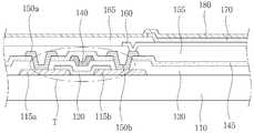
도 1은 종래 기술에 따른 평판표시소자의 구조를 도시한 단면도이다.1 is a cross-sectional view showing the structure of a flat panel display device according to the prior art.
도 1을 참조하면, 기판(110) 상에, 소스 전극(115a), 드레인 전극(115b), 전하의 이동 채널을 형성하는 금속 산화물 반도체층(120), 게이트 절연막인 제 1 절연막(130), 게이트 전극(140), 층간 절연막인 제 2 절연막(145)을 포함하는 박막 트랜지스터(T)가 위치하였다.Referring to FIG. 1, on a
제 2 절연막(145) 상에는 비어홀을 통하여 소스 전극(115a) 및 드레인 전극(115b)과 각각 전기적으로 연결되는 제 1 및 제 2 금속 배선(150a, 150b)이 위치하였다.First and
제 1 및 제 2 금속 배선(150a, 150b)이 위치하는 제 2 절연막(145) 상에는 제 2 금속 배선(150b)의 일부를 노출시키며, 평탄화 또는 패시베이션을 위한 제 3 절연막(155)이 위치하였다. 또한, 제 3 절연막(155) 상에는 제 3 절연막(155)을 관통하여 제 2 금속 배선(150b)과 전기적으로 연결되는 제 1 전극(160), 화소 영역을 구분하는 제 4 절연막(165), 발광층(170) 및 제 2 전극(180)을 포함하는 발광 다이오드가 위치하였다.A portion of the
이상 발광층(170)은 액정층으로 대체 적용될 수도 있었다.The
이상과 같은 박막트랜지스터(T)의 게이트 전극(140) 상에 위치하며, 보호막 역할을 하는 제 2 절연막(145)에는 열처리를 하였으며, 그에 따라 박막트랜지스터(T)의 반도체 특성이 크게 저하되는 문제가 발생하였다.The second
이러한 반도체 특성 저하문제는 박막트랜지스터가 적용되는 소자의 신뢰도 및 수명 저하 문제로 이어졌다.Such a problem of deterioration of semiconductor characteristics has led to a problem of deterioration of reliability and lifetime of devices to which thin film transistors are applied.
따라서, 본 발명은 반도체 특성의 저하를 방지함으로써 소자의 신뢰도 및 수명을 향상시킬 수 있는 박막트랜지스터 및 그 박막트랜지스터를 포함하는 평판표시소자와 그 제조 방법을 제공하는 데 그 목적이 있다.Accordingly, an object of the present invention is to provide a thin film transistor, a flat panel display device including the thin film transistor, and a method of manufacturing the same, which can improve the reliability and lifetime of the device by preventing the deterioration of semiconductor characteristics.
상기 목적을 달성하기 위하여, 본 발명은 기판 상에 위치하는 소스 전극 및 드레인 전극, 소스 전극 및 드레인 전극과 전기적으로 연결되는 금속 산화물 반도체층, 금속 산화물 반도체층 상에 위치하는 게이트 절연막, 게이트 절연막 상에 위 치하며, 게이트 절연막의 금속 산화물 반도체층과 대응되는 위치의 일부 영역을 노출시키는 개구부를 포함하는 보호막, 및 보호막의 개구부 내에 위치하는 게이트 전극을 포함하는 박막트랜지스터를 제공한다.In order to achieve the above object, the present invention provides a source electrode and a drain electrode on the substrate, a metal oxide semiconductor layer electrically connected to the source electrode and the drain electrode, a gate insulating film located on the metal oxide semiconductor layer, the gate insulating film The present invention provides a thin film transistor including a passivation layer including an opening that exposes a portion of a region corresponding to the metal oxide semiconductor layer of the gate insulating layer, and a gate electrode positioned in the opening of the passivation layer.
금속 산화물 반도체층은 아연산화물(ZnO), 인듐아연산화물(InZnO), 인듐갈륨아연산화물(InGaZnO), 아연주석산화물(ZnSnO)로 이루어진 군에서 선택된 하나를 포함할 수 있다.The metal oxide semiconductor layer may include one selected from the group consisting of zinc oxide (ZnO), indium zinc oxide (InZnO), indium gallium zinc oxide (InGaZnO), and zinc tin oxide (ZnSnO).
소스 전극 및 드레인 전극은 10 내지 500nm 범위의 두께일 수 있다.The source electrode and the drain electrode may be in the range of 10 to 500 nm in thickness.
다른 측면에서, 본 발명은 기판, 기판 상에 위치하는 소스 전극 및 드레인 전극, 소스 전극 및 드레인 전극과 전기적으로 연결되는 금속 산화물 반도체층, 금속 산화물 반도체층 상에 위치하는 제 1 절연막, 제 1 절연막 상에 위치하며, 금속 산화물 반도체층과 대응되는 위치에 개구부를 포함하는 제 2 절연막, 제 1 절연막 및 제 2 절연막을 관통하여 드레인 전극의 일부를 노출시키는 제 1 비어홀, 개구부 내에 위치하는 게이트 전극 및 제 1 비어홀을 통하여 드레인 전극과 연결되는 금속배선, 게이트 전극 및 금속배선을 포함한 기판 상에 위치하는 제 3 절연막, 및 제 3 절연막을 관통하여 금속배선과 연결되는 제 1 전극을 포함하는 평판표시소자를 제공한다.In another aspect, the present invention provides a substrate, a source electrode and a drain electrode located on the substrate, a metal oxide semiconductor layer electrically connected to the source electrode and the drain electrode, a first insulating film located on the metal oxide semiconductor layer, a first insulating film A second insulating film including an opening at a position corresponding to the metal oxide semiconductor layer, a first via hole through the first insulating film and the second insulating film to expose a portion of the drain electrode, a gate electrode located in the opening, and A flat panel display device comprising a metal wiring connected to a drain electrode through a first via hole, a third insulating film positioned on a substrate including a gate electrode and a metal wiring, and a first electrode connected to the metal wiring through the third insulating film. To provide.
금속 산화물 반도체층은 아연산화물(ZnO), 인듐아연산화물(InZnO), 인듐갈륨아연산화물(InGaZnO), 아연주석산화물(ZnSnO)로 이루어진 군에서 선택된 하나를 포함할 수 있다.The metal oxide semiconductor layer may include one selected from the group consisting of zinc oxide (ZnO), indium zinc oxide (InZnO), indium gallium zinc oxide (InGaZnO), and zinc tin oxide (ZnSnO).
이상의 평판표시소자는 제 1 전극과 대향하는 제 2 전극을 포함하며, 제 1 및 제 2 전극 사이에 개재된 유기발광층을 포함할 수 있다.The flat panel display device may include a second electrode facing the first electrode and include an organic light emitting layer interposed between the first and second electrodes.
또 다른 측면에서, 본 발명은 기판, 기판 상에 위치하는 소스 전극 및 드레인 전극, 소스 전극 및 드레인 전극과 전기적으로 연결되는 금속 산화물 반도체층, 금속 산화물 반도체층 상에 위치하는 제 1 절연막, 제 1 절연막 상에 위치하며, 금속 산화물 반도체층과 대응되는 위치에 개구부를 포함하는 제 2 절연막, 개구부 내에 위치하는 게이트 전극, 제 1 절연막 및 제 2 절연막을 관통하여 드레인 전극과 전기적으로 연결되는 제 1 전극을 포함하는 평판표시소자를 제공한다.In another aspect, the present invention provides a substrate, a source electrode and a drain electrode located on the substrate, a metal oxide semiconductor layer electrically connected to the source electrode and the drain electrode, a first insulating film located on the metal oxide semiconductor layer, and a first A second insulating film on the insulating film, the second insulating film including an opening at a position corresponding to the metal oxide semiconductor layer, a gate electrode located in the opening, and a first electrode electrically connected to the drain electrode through the first insulating film and the second insulating film It provides a flat panel display device comprising a.
게이트 전극은 10 내지 500nm 범위의 두께일 수 있다.The gate electrode can be a thickness in the range of 10 to 500 nm.
금속 산화물 반도체층은 아연산화물(ZnO), 인듐아연산화물(InZnO), 인듐갈륨아연산화물(InGaZnO), 아연주석산화물(ZnSnO)로 이루어진 군에서 선택된 하나를 포함할 수 있다.The metal oxide semiconductor layer may include one selected from the group consisting of zinc oxide (ZnO), indium zinc oxide (InZnO), indium gallium zinc oxide (InGaZnO), and zinc tin oxide (ZnSnO).
이상의 평판표시소자는 제 1 전극과 대향하는 제 2 전극을 포함하며, 제 1 및 제 2 전극 사이에 개재된 유기발광층을 포함할 수 있다.The flat panel display device may include a second electrode facing the first electrode and include an organic light emitting layer interposed between the first and second electrodes.
이하, 첨부한 도면을 참조하여, 본 발명의 다양한 실시예들을 상세히 설명하도록 한다.Hereinafter, various embodiments of the present invention will be described in detail with reference to the accompanying drawings.
도 2는 도 1에 도시한 종래 기술에 따른 박막트랜지스터의 공정 단계별 각 적층에 대한 열처리 실험의 데이터를 도시한 그래프이다.FIG. 2 is a graph showing data of a heat treatment experiment for each lamination step of a thin film transistor according to the related art shown in FIG. 1.
도 2의 그래프의 X좌표는 게이트 전극의 구동 전압(Vg;[V])의 변화를 나타내고, Y좌표는 게이트 전극의 구동 전압의 변화에 따른 박막트랜지스터(T1)의 구동전류(Pl;[A])의 변화를 나타낸다. 열처리는 300℃의 온도 조건과 10분의 시간 조건하에서 각 적층에 대해 케이스별로 시행되었다.In the graph of FIG. 2, the X coordinate represents a change of the driving voltage Vg; [V] of the gate electrode, and the Y coordinate represents a driving current Pl; [A of the thin film transistor T1 according to the change of the driving voltage of the gate electrode. ]). Heat treatment was performed on a case-by-case basis for each laminate under conditions of temperature of 300 ° C. and time of 10 minutes.
도 1 및 도 2를 참조하면, 제 1 처리 조건(1 treatment)은 기판(110) 상에 소스 전극(115a), 드레인 전극(115b)이 형성되고, 예를 들어, 아연 산화물(ZnO)로 금속 산화물 반도체층(320)이 형성된 상태에서 열처리한 경우이다.1 and 2, in a first treatment condition (1 treatment), a
제 2 처리 조건(2 treatment)은 기판(110) 상에 소스 전극(115a), 드레인 전극(115b), 금속 산화물 반도체층(120) 및 게이트 절연막(145)이 형성된 상태에서 열처리한 경우이다.The second treatment condition (2 treatment) is a case where the heat treatment is performed in a state where the
제 3 처리 조건(3 treatment)은 기판(110) 상에 소스 전극(115a), 드레인 전극(115b), 금속 산화물 반도체층(120) 및 게이트 절연막(145)이 형성되고, 게이트 전극(145)이 증착된 상태에서 열처리 한 경우이다.In a third treatment condition (3 treatment), a
제 4 처리 조건(4 treatment)은 기판(110) 상에 소스 전극(115a), 드레인 전극(115b), 금속 산화물 반도체층(120) 및 게이트 절연막(145)이 형성되고, 게이트 전극(145) 및 제 2 절연막(145)이 형성됨으로써 게이트 전극(145)이 패터닝된 상태에서 열처리 한 경우이다.In a fourth treatment condition (4 treatment), a
제 5 처리 조건(5 treatment)은 게이트 전극(145)이 패터닝되기까지의 과정 중 열처리 없이 진행된 경우의 박막트랜지스터(T1)의 상태를 나타낸다.The fifth treatment condition (5 treatment) represents a state of the thin film transistor T1 when the
이상, 그래프의 결과에 따르면, 열처리 공정이 뒤로 갈수록 소자의 특성이 저하되는 것을 확인할 수 있다. 특히, 게이트 전극(145)이 패터닝된 후의 열처리가 소자의 반도체 특성 저하에 가장 치명적인 영향을 미치는 것을 알 수 있다. As described above, according to the result of the graph, it can be seen that the characteristics of the device are lowered as the heat treatment process goes backward. In particular, it can be seen that the heat treatment after the
따라서, 이하 첨부된 도면을 참조하여 설명할 본 발명의 다양한 실시예들은 위에서 설명한 종래 기술의 문제점을 해결할 수 있는 구조의 박막트랜지스터 및 그 박막트랜지스터를 포함하는 평판표시소자를 제공한다.Accordingly, various embodiments of the present invention to be described below with reference to the accompanying drawings provide a thin film transistor having a structure that can solve the problems of the prior art described above and a flat panel display device including the thin film transistor.
<제 1 실시예><First Embodiment>
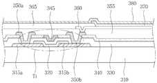
도 3a는 본 발명의 제 1 실시예에 따른 박막트랜지스터의 구조를 도시한 단면도이다.3A is a cross-sectional view illustrating a structure of a thin film transistor according to a first embodiment of the present invention.
도 3a를 참조하면, 기판(310) 상에 소스 전극(315a)과 드레인 전극(315b)이 위치한다. 또한, 소스 전극(315a) 및 드레인 전극(315b)의 일부와 전기적으로 연결되어 전하의 이동 채널을 형성하는 금속 산화물 반도체층(320)이 위치한다.Referring to FIG. 3A, a
소스 전극(315a) 및 드레인 전극(315b)는 외부 전원과 직접 전기적으로 연결되어 각각의 구동 신호를 받을 수 있다.The
금속 산화물 반도체층(320)은 아연산화물(ZnO), 인듐아연산화물(InZnO), 인듐갈륨아연산화물(InGaZnO), 아연주석산화물(ZnSnO)로 이루어진 군에서 선택된 하나를 포함하도록 형성될 수 있다. 이상과 같이 금속 산화물로 반도체층(320)이 형성되는 경우, 비정질 실리콘 또는 폴리 실리콘으로 반도체층이 형성되는 경우보다 낮은 온도에서 반도체층(320)을 형성할 수 있으며, 더 높은 이동도(mobility)를 얻을 수 있다.The metal
금속 산화물 반도체층(320) 상에는 게이트 절연막인 제 1 절연막(330)과 층간 절연막인 제 2 절연막(340)이 위치한다.The first insulating
제 2 절연막(340)에는 금속 산화물 반도체층(320)과 대응되는 위치의 제 1 절연막(330)을 노출시키는 게이트홀이 형성된다.Gate holes are formed in the second insulating
게이트홀 내부에는 게이트 전극(345)이 형성된다. 게이트 전극(345)은 예를 들어, 스퍼터링(Sputtering) 방법으로 형성될 수 있으며, 규소 질화물(SiNx), 규소 산화물(SiOx), 규소 질산화물(SiOxNy), 알루미늄 산화물(AlOx), 알루미늄이 도핑된 아연 산화물(Al doped ZnO), 갈륨이 도핑된 아연 산화물(Ga doped ZnO)로 이루어진 군에서 선택된 하나를 포함할 수 있다.The
또한, 게이트 전극(345)은 10 내지 500nm 범위의 두께로 형성될 수 있다. 이는 게이트 전극(345)의 두께가 10nm 미만일 경우, 저항이 낮아 사용 불가하며, 두께가 500nm를 초과할 경우 재료비가 증가하고, 박막트랜지스터 상에 두 개의 전극 및 발광층을 포함하는 픽셀부가 형성될 경우, 별도의 평탄화 공정이 추가될 수 있기 때문이다.In addition, the
이상과 같은 구조를 갖는 본 발명의 제 1 실시예에 따른 박막트랜지스터는 게이트 전극(345)이 박막트랜지스터의 최상부에 위치하며, 제 1 및 제 2 절연막(330, 340)이 열처리를 통하여 패터닝된 후에 형성되므로 반도체 특성의 저하를 방지할 수 있다.In the thin film transistor according to the first embodiment of the present invention having the above structure, the
도 3b는 본 발명의 제 1 실시예에 따른 평판표시소자의 구조를 도시한 단면 도이다.3B is a cross-sectional view showing the structure of a flat panel display device according to a first embodiment of the present invention.
도 3b를 참조하면, 도 3a에 도시된 바와 같은 구조를 갖는 박막트랜지스터(T1)가 기판(310) 상에 위치한다.Referring to FIG. 3B, a thin film transistor T1 having a structure as shown in FIG. 3A is positioned on the
박막트랜지스터(T1)는 소스 전극(315a), 드레인 전극(315b), 전하의 이동 채널을 형성하는 금속 산화물 반도체층(320), 게이트 절연막인 제 1 절연막(330), 층간 절연막인 제 2 절연막(345) 및 게이트 전극(340)을 포함한다.The thin film transistor T1 includes a
제 1 및 제 2 절연막(330, 340)에는 소스(315a) 및 드레인 전극(315b)을 노출시키는 제 1 및 제 2 비어홀이 형성되고, 금속 산화물 반도체층(320)과 대응되는 위치의 제 1 절연막(330)을 노출시키는 게이트홀이 형성된다. 제 1 및 제 2 금속 배선(350a, 350b)은 제 1 및 제 2 비어홀을 통해 소스 전극(315a) 및 드레인 전극(315b)과 각각 전기적으로 연결된다. 소스 전극(315a) 및 드레인 전극(315b)은 제 1 및 제 2 금속 배선(350a, 350b)을 통해 외부 전원과 전기적으로 연결되어 구동 신호를 받을 수 있다.First and second via holes exposing the
또한, 게이트 전극(340)은 게이트홀의 내측에 형성되며, 제 2 절연막(340)과 동일한 높이 층으로 형성될 수 있다. 이와 같은 구조는 평탄화공정을 생략하거나 단순화시킬 수 있다.In addition, the
박막 트랜지스터(T1) 상에는 제 2 금속 배선(350b)의 일부를 노출시키며, 평탄화 또는 패시베이션을 위한 제 3 절연막(355)이 위치한다. 또한, 제 3 절연막(355) 상에는 제 3 절연막(355)을 관통하여 제 2 금속 배선(350b)과 전기적으로 연결되는 제 1 전극(360), 화소 영역을 구분하는 제 4 절연막(365), 발광층(370) 및 제 2 전극(380)을 포함하는 발광 다이오드가 위치한다.A portion of the
도 4a 내지 도 4e는 본 발명의 제 1 실시예에 따른 평판표시소자의 공정 단계별 상태를 도시한 단면도이다.4A to 4E are cross-sectional views illustrating states of process steps of the flat panel display device according to the first embodiment of the present invention.
이하, 도 4a 내지 도 4e를 참조하여, 이상과 같은 본 발명의 제 1 실시예에 따른 평판표시소자의 구조를 공정 측면에서 설명하기로 한다.Hereinafter, the structure of the flat panel display device according to the first embodiment of the present invention will be described in terms of processes with reference to FIGS. 4A to 4E.
도 4a를 참조하면, 기판(310) 상에 증착법으로 소스 전극(315a)과 드레인 전극(315b)을 형성한다. 소스 전극(315a)과 드레인 전극(315b) 상에는 전하의 이동 채널을 형성하는 금속 산화물 반도체층(320)을 형성한다. 금속 산화물 반도체층(320)은 아연산화물(ZnO), 인듐아연산화물(InZnO), 인듐갈륨아연산화물(InGaZnO), 아연주석산화물(ZnSnO)로 이루어진 군에서 선택된 하나를 포함하도록 형성될 수 있다.Referring to FIG. 4A, a
이상과 같이 금속 산화물로 반도체층(320)이 형성되는 경우, 비정질 실리콘 또는 폴리 실리콘으로 반도체층이 형성되는 경우보다 낮은 온도에서 반도체층(320)을 형성할 수 있으며, 더 높은 이동도(mobility)를 얻을 수 있다.As described above, when the
도 4b 및 4c를 참조하면, 소스 전극(315a)와 드레인 전극(315b) 및 금속 산화물 반도체층(320)이 형성된 기판(310) 상에 게이트 절연막인 제 1 절연막(330)과 층간 절연막인 제 2 절연막(340)을 형성한다.4B and 4C, a first
제 1 및 제 2 절연막(330, 340)에는 소스 전극(315a)와 드레인 전극(315b)을 각각 노출시키는 제 1 비어홀(H1)과 제 2 비어홀(H2)을 형성한다. 또한, 금속 산화 물 반도체층(320)과 대응되는 위치의 제 1 절연막(330)을 노출시키는 게이트홀(H3)을 형성한다. 제 1 및 제 2 비어홀(H1, H2)과 게이트홀(H3)은 에칭에 의한 식각으로 형성할 수 있으나 그 형성 방법은 이에 국한되지 않는다. 따라서, 제 1 및 제 2 절연막(330, 340)은 성막 시 마스크를 이용한 선택적 증착법(deposition)으로 형성될 수도 있다.A first via hole H1 and a second via hole H2 exposing the
도 4d를 참조하면, 제 1 비어홀(H1) 및 제 2 비어홀(H2)을 통해 소스 전극(315a) 및 드레인 전극(315b)과 각각 전기적으로 연결되는 제 1 금속 배선(350a)과 제 2 금속 배선(350b)을 스퍼터링(Sputtering) 방법으로 형성할 수 있다.Referring to FIG. 4D, a
제 1 및 제 2 금속 배선(350a, 350b)은 10 내지 500nm 범위의 두께로 형성될 수 있다. 이는 제 1 및 제 2 금속 배선(350a, 350b)의 두께가 10nm 미만일 경우, 저항이 낮아 사용 불가하며, 두께가 500nm를 초과할 경우 재료비가 증가하고, 별도의 평탄화 공정이 추가될 수 있기 때문이다.The first and
게이트홀(H3) 내부에는 게이트 전극(345)을 형성한다. 게이트 전극(345)은 예를 들어, 스퍼터링(Sputtering) 방법으로 형성할 수 있으며, 규소 질화물(SiNx), 규소 산화물(SiOx), 규소 질산화물(SiOxNy), 알루미늄 산화물(AlOx), 알루미늄이 도핑된 아연 산화물(Al doped ZnO), 갈륨이 도핑된 아연 산화물(Ga doped ZnO)로 이루어진 군에서 선택된 하나를 포함할 수 있다.A
또한, 게이트 전극(345)은 10 내지 500nm 범위의 두께로 형성될 수 있다. 이는 게이트 전극(345)의 두께가 10nm 미만일 경우, 저항이 낮아 사용 불가하며, 두께가 500nm를 초과할 경우 재료비가 증가하고, 별도의 평탄화 공정이 추가될 수 있 기 때문이다.In addition, the
도 4e를 참조하면, 이상과 같이 박막트랜지스터가 형성된 기판(310) 상에 제 2 금속 배선(350b)의 일부를 노출시키며, 평탄화 또는 패시베이션을 위한 제 3 절연막(355)을 형성한다. 또한, 제 3 절연막(355) 상에는 제 3 절연막(355)을 관통하여 제 2 금속 배선(350b)과 전기적으로 연결되는 제 1 전극(360), 화소 영역을 구분하는 제 4 절연막(365), 발광층(370) 및 제 2 전극(380)을 포함하는 발광 다이오드를 형성한다.Referring to FIG. 4E, a portion of the
이상과 같은 구조 및 제조 공정에 따른 본 발명의 제 1 실시예의 평판표시소자는 박막트랜지스터(T1)의 최상부에 게이트 전극(345)이 위치하며, 제 1 및 제 2 절연막(330, 340)이 열처리를 통하여 패터닝된 후에 형성되므로 반도체 특성의 저하를 방지할 수 있다.In the flat panel display device according to the first embodiment of the present invention according to the above structure and manufacturing process, the
<제 2 실시예>Second Embodiment
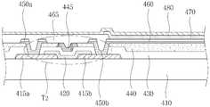
도 5는 본 발명의 제 2 실시예에 따른 평판표시소자의 구조를 도시한 단면도이다.5 is a cross-sectional view illustrating a structure of a flat panel display device according to a second exemplary embodiment of the present invention.
도 5를 참조하면, 기판(410) 상에 소스 전극(415a)과 드레인 전극(415b)이 위치한다. 또한, 소스 전극(415a) 및 드레인 전극(415b)의 일부와 전기적으로 연결되어 전하의 이동 채널을 형성하는 금속 산화물 반도체층(420)이 위치한다.Referring to FIG. 5, a
금속 산화물 반도체층(320) 상에는 게이트 절연막인 제 1 절연막(430)과 층간 절연막인 제 2 절연막(440)이 위치한다.The first insulating
제 2 절연막(440)에는 금속 산화물 반도체층(420)과 대응되는 위치의 제 1 절연막(430)을 노출시키는 게이트홀이 형성된다.A gate hole exposing the first insulating
게이트홀 내부에는 게이트 전극(445)이 형성된다. 게이트 전극(445)은 제 2 절연막(440)과 동일한 높이로 형성될 수 있으며, 예를 들어, 스퍼터링(Sputtering) 방법으로 형성될 수 있다. 또한, 게이트 전극(445)은 규소 질화물(SiNx), 규소 산화물(SiOx), 규소 질산화물(SiOxNy), 알루미늄 산화물(AlOx), 알루미늄이 도핑된 아연 산화물(Al doped ZnO), 갈륨이 도핑된 아연 산화물(Ga doped ZnO)로 이루어진 군에서 선택된 하나를 포함할 수 있다.The
또한, 게이트 전극(445)은 10 내지 500nm 범위의 두께로 형성될 수 있다. 이는 게이트 전극(345)의 두께가 10nm 미만일 경우, 저항이 낮아 사용 불가하며, 두께가 500nm를 초과할 경우 재료비가 증가하고, 별도의 평탄화 공정이 추가될 수 있기 때문이다.In addition, the
박막 트랜지스터(T2) 상에는 제 2 금속 배선(450b)의 일부를 노출시키며, 평탄화 또는 패시베이션을 위한 제 3 절연막(455)이 위치한다. 또한, 제 3 절연막(455) 상에는 제 3 절연막(455)을 관통하여 제 2 금속 배선(450b)과 전기적으로 연결되는 제 1 전극(460), 화소 영역을 구분하는 제 4 절연막(465), 발광층(470) 및 제 2 전극(480)을 포함하는 발광 다이오드가 위치한다.A portion of the
이상과 같은 구조를 갖는 본 발명의 제 2 실시예에 따른 평판표시소자는 박막트랜지스터(T2)의 최상부에 게이트 전극(445)이 위치하며, 제 1 및 제 2 절연막(430, 440)이 열처리를 통하여 패터닝된 후에 형성되므로 반도체 특성의 저하를 방지할 수 있다.In the flat panel display device according to the second embodiment of the present invention having the structure as described above, the
이상 본 발명의 제 1 및 제 2 실시예에서는 박막트랜지스터가 전계발광소자의 구동부로 적용된 경우를 예를 들어 설명하였으나, 본 발명에 따른 박막트랜지스터는 액정표시장치를 비롯한 다양한 평판표시소자의 구동부로도 적용 가능하다.In the first and second embodiments of the present invention, the thin film transistor is applied as a driving unit of an electroluminescent device, for example. However, the thin film transistor according to the present invention is also used as a driving unit of various flat panel display devices including a liquid crystal display device. Applicable
이상 본 발명의 다양한 실시예들에 따른 평판표시소자의 발광층은 유기물, 무기물 중 어느 하나 또는 하나 이상을 포함할 수 있다.The light emitting layer of the flat panel display device according to various embodiments of the present invention may include any one or more of an organic material and an inorganic material.
이상 본 발명이 속하는 기술분야의 당업자는 본 발명이 그 기술적 사상이나 필수적 특징을 변경하지 않고서 다른 구체적인 형태로 실시될 수 있다는 것을 이해할 수 있을 것이다. 그러므로 이상에서 기술한 실시예는 모든 면에서 예시적인 것이며 한정적인 것이 아닌 것으로서 이해되어야 하고, 본 발명의 범위는 상기 상세한 설명보다는 후술하는 특허청구범위에 의하여 나타내어지며, 특허청구범위의 의미 및 범위 그리고 그 등가개념으로부터 도출되는 모든 변경 또는 변형된 형태가 본 발명의 범위에 포함되는 것으로 해석되어야 한다.Those skilled in the art to which the present invention pertains will understand that the present invention can be implemented in other specific forms without changing the technical spirit or essential features. Therefore, the above-described embodiments are to be understood as illustrative and not restrictive in all respects, and the scope of the present invention is indicated by the appended claims rather than the foregoing description, and the meaning and scope of the claims and All changes or modifications derived from the equivalent concept should be interpreted as being included in the scope of the present invention.
본 발명은 반도체 특성의 저하를 방지함으로써 소자의 신뢰도 및 수명을 향상시킬 수 있는 박막트랜지스터 및 그 박막트랜지스터를 포함하는 평판표시소자와 그 제조 방법을 제공할 수 있다.The present invention can provide a thin film transistor, a flat panel display device including the thin film transistor, and a method of manufacturing the same, which can improve the reliability and life of the device by preventing the deterioration of semiconductor characteristics.
Claims (10)
Translated fromKoreanPriority Applications (1)
| Application Number | Priority Date | Filing Date | Title |
|---|---|---|---|
| KR1020060124158AKR100793105B1 (en) | 2006-12-07 | 2006-12-07 | Flat panel display device including thin film transistor and thin film transistor and manufacturing method thereof |
Applications Claiming Priority (1)
| Application Number | Priority Date | Filing Date | Title |
|---|---|---|---|
| KR1020060124158AKR100793105B1 (en) | 2006-12-07 | 2006-12-07 | Flat panel display device including thin film transistor and thin film transistor and manufacturing method thereof |
Publications (1)
| Publication Number | Publication Date |
|---|---|
| KR100793105B1true KR100793105B1 (en) | 2008-01-10 |
Family
ID=39217297
Family Applications (1)
| Application Number | Title | Priority Date | Filing Date |
|---|---|---|---|
| KR1020060124158AExpired - Fee RelatedKR100793105B1 (en) | 2006-12-07 | 2006-12-07 | Flat panel display device including thin film transistor and thin film transistor and manufacturing method thereof |
Country Status (1)
| Country | Link |
|---|---|
| KR (1) | KR100793105B1 (en) |
Cited By (4)
| Publication number | Priority date | Publication date | Assignee | Title |
|---|---|---|---|---|
| KR101790062B1 (en) | 2011-08-24 | 2017-10-25 | 엘지디스플레이 주식회사 | Thin Film Transistor using Oxidized Semiconducotor and Method for fabricating the same |
| US11049733B2 (en) | 2010-02-26 | 2021-06-29 | Semiconductor Energy Laboratory Co., Ltd. | Method for manufacturing semiconductor device |
| JP2023052234A (en)* | 2009-03-05 | 2023-04-11 | 株式会社半導体エネルギー研究所 | EL display device |
| JP2023107852A (en)* | 2022-04-07 | 2023-08-03 | 株式会社半導体エネルギー研究所 | semiconductor equipment |
Citations (4)
| Publication number | Priority date | Publication date | Assignee | Title |
|---|---|---|---|---|
| JPS6341077A (en) | 1986-08-06 | 1988-02-22 | Nippon Sheet Glass Co Ltd | Manufacturing method of thin film transistor |
| JP2006186119A (en) | 2004-12-28 | 2006-07-13 | Casio Comput Co Ltd | Thin film transistor and manufacturing method thereof |
| US7145174B2 (en) | 2004-03-12 | 2006-12-05 | Hewlett-Packard Development Company, Lp. | Semiconductor device |
| KR20070035373A (en)* | 2005-09-27 | 2007-03-30 | 삼성에스디아이 주식회사 | Transparent thin film transistor and manufacturing method thereof |
- 2006
- 2006-12-07KRKR1020060124158Apatent/KR100793105B1/ennot_activeExpired - Fee Related
Patent Citations (4)
| Publication number | Priority date | Publication date | Assignee | Title |
|---|---|---|---|---|
| JPS6341077A (en) | 1986-08-06 | 1988-02-22 | Nippon Sheet Glass Co Ltd | Manufacturing method of thin film transistor |
| US7145174B2 (en) | 2004-03-12 | 2006-12-05 | Hewlett-Packard Development Company, Lp. | Semiconductor device |
| JP2006186119A (en) | 2004-12-28 | 2006-07-13 | Casio Comput Co Ltd | Thin film transistor and manufacturing method thereof |
| KR20070035373A (en)* | 2005-09-27 | 2007-03-30 | 삼성에스디아이 주식회사 | Transparent thin film transistor and manufacturing method thereof |
Cited By (12)
| Publication number | Priority date | Publication date | Assignee | Title |
|---|---|---|---|---|
| JP2023052234A (en)* | 2009-03-05 | 2023-04-11 | 株式会社半導体エネルギー研究所 | EL display device |
| US11955537B2 (en) | 2009-03-05 | 2024-04-09 | Semiconductor Energy Laboratory Co., Ltd. | Semiconductor device and method for manufacturing the same |
| JP7505054B2 (en) | 2009-03-05 | 2024-06-24 | 株式会社半導体エネルギー研究所 | EL display device |
| JP2024120915A (en)* | 2009-03-05 | 2024-09-05 | 株式会社半導体エネルギー研究所 | EL display device |
| US12336303B2 (en) | 2009-03-05 | 2025-06-17 | Semiconductor Energy Laboratory Co., Ltd. | Semiconductor device and method for manufacturing the same |
| JP7734236B2 (en) | 2009-03-05 | 2025-09-04 | 株式会社半導体エネルギー研究所 | EL display device |
| US11049733B2 (en) | 2010-02-26 | 2021-06-29 | Semiconductor Energy Laboratory Co., Ltd. | Method for manufacturing semiconductor device |
| US11682562B2 (en) | 2010-02-26 | 2023-06-20 | Semiconductor Energy Laboratory Co., Ltd. | Method for manufacturing semiconductor device |
| US12033867B2 (en) | 2010-02-26 | 2024-07-09 | Semiconductor Energy Laboratory Co., Ltd. | Method for manufacturing semiconductor device |
| KR101790062B1 (en) | 2011-08-24 | 2017-10-25 | 엘지디스플레이 주식회사 | Thin Film Transistor using Oxidized Semiconducotor and Method for fabricating the same |
| JP2023107852A (en)* | 2022-04-07 | 2023-08-03 | 株式会社半導体エネルギー研究所 | semiconductor equipment |
| JP7474369B2 (en) | 2022-04-07 | 2024-04-24 | 株式会社半導体エネルギー研究所 | Semiconductor Device |
Similar Documents
| Publication | Publication Date | Title |
|---|---|---|
| US11075221B2 (en) | Thin-film transistor substrate having overlapping thin-film transistor | |
| KR101073542B1 (en) | Organic light emitting diode display and method for manufacturing the same | |
| CN101794809B (en) | Organic light emitting display device and method of manufacturing the same | |
| US9768310B2 (en) | Thin film transistor, organic light-emitting diode display including the same, and manufacturing method thereof | |
| KR101117642B1 (en) | Organic light emitting diode display and method for manufacturing the same | |
| KR101065407B1 (en) | Organic light emitting display and manufacturing method thereof | |
| US20100182223A1 (en) | Organic light emitting display device | |
| KR100975204B1 (en) | Thin film transistor, its manufacturing method, and flat panel display device comprising thin film transistor | |
| US8022398B2 (en) | Thin film transistor, method of forming the same and flat panel display device having the same | |
| KR20090124527A (en) | Thin film transistor, its manufacturing method, and flat panel display device comprising thin film transistor | |
| KR20090105558A (en) | Thin film transistor, its manufacturing method, and flat panel display device comprising thin film transistor | |
| KR100786294B1 (en) | Organic electroluminescent display and manufacturing method thereof | |
| KR20110032360A (en) | Organic light emitting display and manufacturing method thereof | |
| KR20050098596A (en) | Organic electro-luminescent display device and fabricating the same | |
| KR20090105561A (en) | Semiconductor device and flat panel display device having same | |
| KR100793105B1 (en) | Flat panel display device including thin film transistor and thin film transistor and manufacturing method thereof | |
| US20130001566A1 (en) | Back plane for use in flat panel displays and method of manufacturing the back plane | |
| KR100941855B1 (en) | Thin film transistor, its manufacturing method, and flat panel display device comprising thin film transistor | |
| KR20150021212A (en) | Method for fabricating Organic Electroluminescence Device and the Organic Electroluminescence Device fabricated by the method | |
| KR20100029350A (en) | Organic light emitting display and method for fabricating the same | |
| WO2023112328A1 (en) | Display device |
Legal Events
| Date | Code | Title | Description |
|---|---|---|---|
| A201 | Request for examination | ||
| PA0109 | Patent application | St.27 status event code:A-0-1-A10-A12-nap-PA0109 | |
| PA0201 | Request for examination | St.27 status event code:A-1-2-D10-D11-exm-PA0201 | |
| D13-X000 | Search requested | St.27 status event code:A-1-2-D10-D13-srh-X000 | |
| R17-X000 | Change to representative recorded | St.27 status event code:A-3-3-R10-R17-oth-X000 | |
| D14-X000 | Search report completed | St.27 status event code:A-1-2-D10-D14-srh-X000 | |
| E701 | Decision to grant or registration of patent right | ||
| PE0701 | Decision of registration | St.27 status event code:A-1-2-D10-D22-exm-PE0701 | |
| GRNT | Written decision to grant | ||
| PR0701 | Registration of establishment | St.27 status event code:A-2-4-F10-F11-exm-PR0701 | |
| PR1002 | Payment of registration fee | St.27 status event code:A-2-2-U10-U11-oth-PR1002 Fee payment year number:1 | |
| PG1601 | Publication of registration | St.27 status event code:A-4-4-Q10-Q13-nap-PG1601 | |
| PN2301 | Change of applicant | St.27 status event code:A-5-5-R10-R13-asn-PN2301 St.27 status event code:A-5-5-R10-R11-asn-PN2301 | |
| R18-X000 | Changes to party contact information recorded | St.27 status event code:A-5-5-R10-R18-oth-X000 | |
| R18-X000 | Changes to party contact information recorded | St.27 status event code:A-5-5-R10-R18-oth-X000 | |
| PR1001 | Payment of annual fee | St.27 status event code:A-4-4-U10-U11-oth-PR1001 Fee payment year number:4 | |
| FPAY | Annual fee payment | Payment date:20111220 Year of fee payment:5 | |
| PR1001 | Payment of annual fee | St.27 status event code:A-4-4-U10-U11-oth-PR1001 Fee payment year number:5 | |
| FPAY | Annual fee payment | Payment date:20121227 Year of fee payment:6 | |
| PR1001 | Payment of annual fee | St.27 status event code:A-4-4-U10-U11-oth-PR1001 Fee payment year number:6 | |
| LAPS | Lapse due to unpaid annual fee | ||
| PC1903 | Unpaid annual fee | St.27 status event code:A-4-4-U10-U13-oth-PC1903 Not in force date:20140104 Payment event data comment text:Termination Category : DEFAULT_OF_REGISTRATION_FEE | |
| PC1903 | Unpaid annual fee | St.27 status event code:N-4-6-H10-H13-oth-PC1903 Ip right cessation event data comment text:Termination Category : DEFAULT_OF_REGISTRATION_FEE Not in force date:20140104 | |
| PN2301 | Change of applicant | St.27 status event code:A-5-5-R10-R13-asn-PN2301 St.27 status event code:A-5-5-R10-R11-asn-PN2301 | |
| PN2301 | Change of applicant | St.27 status event code:A-5-5-R10-R13-asn-PN2301 St.27 status event code:A-5-5-R10-R11-asn-PN2301 | |
| P22-X000 | Classification modified | St.27 status event code:A-4-4-P10-P22-nap-X000 | |
| P22-X000 | Classification modified | St.27 status event code:A-4-4-P10-P22-nap-X000 |