KR100791576B1 - Stacked package of ball grid array type - Google Patents
Stacked package of ball grid array typeDownload PDFInfo
- Publication number
- KR100791576B1 KR100791576B1KR1020050096659AKR20050096659AKR100791576B1KR 100791576 B1KR100791576 B1KR 100791576B1KR 1020050096659 AKR1020050096659 AKR 1020050096659AKR 20050096659 AKR20050096659 AKR 20050096659AKR 100791576 B1KR100791576 B1KR 100791576B1
- Authority
- KR
- South Korea
- Prior art keywords
- package
- wiring board
- chip
- semiconductor chip
- bonding
- Prior art date
- Legal status (The legal status is an assumption and is not a legal conclusion. Google has not performed a legal analysis and makes no representation as to the accuracy of the status listed.)
- Expired - Fee Related
Links
Images


Classifications
- H—ELECTRICITY
- H01—ELECTRIC ELEMENTS
- H01L—SEMICONDUCTOR DEVICES NOT COVERED BY CLASS H10
- H01L23/00—Details of semiconductor or other solid state devices
- H01L23/48—Arrangements for conducting electric current to or from the solid state body in operation, e.g. leads, terminal arrangements ; Selection of materials therefor
- H01L23/488—Arrangements for conducting electric current to or from the solid state body in operation, e.g. leads, terminal arrangements ; Selection of materials therefor consisting of soldered or bonded constructions
- H01L23/498—Leads, i.e. metallisations or lead-frames on insulating substrates, e.g. chip carriers
- H01L23/49833—Leads, i.e. metallisations or lead-frames on insulating substrates, e.g. chip carriers the chip support structure consisting of a plurality of insulating substrates
- H—ELECTRICITY
- H01—ELECTRIC ELEMENTS
- H01L—SEMICONDUCTOR DEVICES NOT COVERED BY CLASS H10
- H01L23/00—Details of semiconductor or other solid state devices
- H01L23/12—Mountings, e.g. non-detachable insulating substrates
- H—ELECTRICITY
- H01—ELECTRIC ELEMENTS
- H01L—SEMICONDUCTOR DEVICES NOT COVERED BY CLASS H10
- H01L23/00—Details of semiconductor or other solid state devices
- H01L23/12—Mountings, e.g. non-detachable insulating substrates
- H01L23/13—Mountings, e.g. non-detachable insulating substrates characterised by the shape
- H—ELECTRICITY
- H01—ELECTRIC ELEMENTS
- H01L—SEMICONDUCTOR DEVICES NOT COVERED BY CLASS H10
- H01L23/00—Details of semiconductor or other solid state devices
- H01L23/48—Arrangements for conducting electric current to or from the solid state body in operation, e.g. leads, terminal arrangements ; Selection of materials therefor
- H01L23/488—Arrangements for conducting electric current to or from the solid state body in operation, e.g. leads, terminal arrangements ; Selection of materials therefor consisting of soldered or bonded constructions
- H01L23/498—Leads, i.e. metallisations or lead-frames on insulating substrates, e.g. chip carriers
- H01L23/49811—Additional leads joined to the metallisation on the insulating substrate, e.g. pins, bumps, wires, flat leads
- H01L23/49816—Spherical bumps on the substrate for external connection, e.g. ball grid arrays [BGA]
- H—ELECTRICITY
- H01—ELECTRIC ELEMENTS
- H01L—SEMICONDUCTOR DEVICES NOT COVERED BY CLASS H10
- H01L25/00—Assemblies consisting of a plurality of semiconductor or other solid state devices
- H01L25/03—Assemblies consisting of a plurality of semiconductor or other solid state devices all the devices being of a type provided for in a single subclass of subclasses H10B, H10D, H10F, H10H, H10K or H10N, e.g. assemblies of rectifier diodes
- H01L25/10—Assemblies consisting of a plurality of semiconductor or other solid state devices all the devices being of a type provided for in a single subclass of subclasses H10B, H10D, H10F, H10H, H10K or H10N, e.g. assemblies of rectifier diodes the devices having separate containers
- H01L25/105—Assemblies consisting of a plurality of semiconductor or other solid state devices all the devices being of a type provided for in a single subclass of subclasses H10B, H10D, H10F, H10H, H10K or H10N, e.g. assemblies of rectifier diodes the devices having separate containers the devices being integrated devices of class H10
- H—ELECTRICITY
- H01—ELECTRIC ELEMENTS
- H01L—SEMICONDUCTOR DEVICES NOT COVERED BY CLASS H10
- H01L2224/00—Indexing scheme for arrangements for connecting or disconnecting semiconductor or solid-state bodies and methods related thereto as covered by H01L24/00
- H01L2224/01—Means for bonding being attached to, or being formed on, the surface to be connected, e.g. chip-to-package, die-attach, "first-level" interconnects; Manufacturing methods related thereto
- H01L2224/26—Layer connectors, e.g. plate connectors, solder or adhesive layers; Manufacturing methods related thereto
- H01L2224/31—Structure, shape, material or disposition of the layer connectors after the connecting process
- H01L2224/32—Structure, shape, material or disposition of the layer connectors after the connecting process of an individual layer connector
- H01L2224/321—Disposition
- H01L2224/32151—Disposition the layer connector connecting between a semiconductor or solid-state body and an item not being a semiconductor or solid-state body, e.g. chip-to-substrate, chip-to-passive
- H01L2224/32221—Disposition the layer connector connecting between a semiconductor or solid-state body and an item not being a semiconductor or solid-state body, e.g. chip-to-substrate, chip-to-passive the body and the item being stacked
- H01L2224/32225—Disposition the layer connector connecting between a semiconductor or solid-state body and an item not being a semiconductor or solid-state body, e.g. chip-to-substrate, chip-to-passive the body and the item being stacked the item being non-metallic, e.g. insulating substrate with or without metallisation
- H—ELECTRICITY
- H01—ELECTRIC ELEMENTS
- H01L—SEMICONDUCTOR DEVICES NOT COVERED BY CLASS H10
- H01L2224/00—Indexing scheme for arrangements for connecting or disconnecting semiconductor or solid-state bodies and methods related thereto as covered by H01L24/00
- H01L2224/01—Means for bonding being attached to, or being formed on, the surface to be connected, e.g. chip-to-package, die-attach, "first-level" interconnects; Manufacturing methods related thereto
- H01L2224/42—Wire connectors; Manufacturing methods related thereto
- H01L2224/47—Structure, shape, material or disposition of the wire connectors after the connecting process
- H01L2224/48—Structure, shape, material or disposition of the wire connectors after the connecting process of an individual wire connector
- H01L2224/481—Disposition
- H01L2224/48151—Connecting between a semiconductor or solid-state body and an item not being a semiconductor or solid-state body, e.g. chip-to-substrate, chip-to-passive
- H01L2224/48221—Connecting between a semiconductor or solid-state body and an item not being a semiconductor or solid-state body, e.g. chip-to-substrate, chip-to-passive the body and the item being stacked
- H01L2224/48225—Connecting between a semiconductor or solid-state body and an item not being a semiconductor or solid-state body, e.g. chip-to-substrate, chip-to-passive the body and the item being stacked the item being non-metallic, e.g. insulating substrate with or without metallisation
- H01L2224/4824—Connecting between the body and an opposite side of the item with respect to the body
- H—ELECTRICITY
- H01—ELECTRIC ELEMENTS
- H01L—SEMICONDUCTOR DEVICES NOT COVERED BY CLASS H10
- H01L2224/00—Indexing scheme for arrangements for connecting or disconnecting semiconductor or solid-state bodies and methods related thereto as covered by H01L24/00
- H01L2224/73—Means for bonding being of different types provided for in two or more of groups H01L2224/10, H01L2224/18, H01L2224/26, H01L2224/34, H01L2224/42, H01L2224/50, H01L2224/63, H01L2224/71
- H01L2224/732—Location after the connecting process
- H01L2224/73201—Location after the connecting process on the same surface
- H01L2224/73215—Layer and wire connectors
- H—ELECTRICITY
- H01—ELECTRIC ELEMENTS
- H01L—SEMICONDUCTOR DEVICES NOT COVERED BY CLASS H10
- H01L2224/00—Indexing scheme for arrangements for connecting or disconnecting semiconductor or solid-state bodies and methods related thereto as covered by H01L24/00
- H01L2224/73—Means for bonding being of different types provided for in two or more of groups H01L2224/10, H01L2224/18, H01L2224/26, H01L2224/34, H01L2224/42, H01L2224/50, H01L2224/63, H01L2224/71
- H01L2224/732—Location after the connecting process
- H01L2224/73251—Location after the connecting process on different surfaces
- H01L2224/73265—Layer and wire connectors
- H—ELECTRICITY
- H01—ELECTRIC ELEMENTS
- H01L—SEMICONDUCTOR DEVICES NOT COVERED BY CLASS H10
- H01L2225/00—Details relating to assemblies covered by the group H01L25/00 but not provided for in its subgroups
- H01L2225/03—All the devices being of a type provided for in the same main group of the same subclass of class H10, e.g. assemblies of rectifier diodes
- H01L2225/10—All the devices being of a type provided for in the same main group of the same subclass of class H10, e.g. assemblies of rectifier diodes the devices having separate containers
- H01L2225/1005—All the devices being of a type provided for in the same main group of the same subclass of class H10, e.g. assemblies of rectifier diodes the devices having separate containers the devices being integrated devices of class H10
- H01L2225/1011—All the devices being of a type provided for in the same main group of the same subclass of class H10, e.g. assemblies of rectifier diodes the devices having separate containers the devices being integrated devices of class H10 the containers being in a stacked arrangement
- H01L2225/1017—All the devices being of a type provided for in the same main group of the same subclass of class H10, e.g. assemblies of rectifier diodes the devices having separate containers the devices being integrated devices of class H10 the containers being in a stacked arrangement the lowermost container comprising a device support
- H01L2225/1023—All the devices being of a type provided for in the same main group of the same subclass of class H10, e.g. assemblies of rectifier diodes the devices having separate containers the devices being integrated devices of class H10 the containers being in a stacked arrangement the lowermost container comprising a device support the support being an insulating substrate
- H—ELECTRICITY
- H01—ELECTRIC ELEMENTS
- H01L—SEMICONDUCTOR DEVICES NOT COVERED BY CLASS H10
- H01L2225/00—Details relating to assemblies covered by the group H01L25/00 but not provided for in its subgroups
- H01L2225/03—All the devices being of a type provided for in the same main group of the same subclass of class H10, e.g. assemblies of rectifier diodes
- H01L2225/10—All the devices being of a type provided for in the same main group of the same subclass of class H10, e.g. assemblies of rectifier diodes the devices having separate containers
- H01L2225/1005—All the devices being of a type provided for in the same main group of the same subclass of class H10, e.g. assemblies of rectifier diodes the devices having separate containers the devices being integrated devices of class H10
- H01L2225/1011—All the devices being of a type provided for in the same main group of the same subclass of class H10, e.g. assemblies of rectifier diodes the devices having separate containers the devices being integrated devices of class H10 the containers being in a stacked arrangement
- H01L2225/1041—Special adaptations for top connections of the lowermost container, e.g. redistribution layer, integral interposer
- H—ELECTRICITY
- H01—ELECTRIC ELEMENTS
- H01L—SEMICONDUCTOR DEVICES NOT COVERED BY CLASS H10
- H01L24/00—Arrangements for connecting or disconnecting semiconductor or solid-state bodies; Methods or apparatus related thereto
- H01L24/01—Means for bonding being attached to, or being formed on, the surface to be connected, e.g. chip-to-package, die-attach, "first-level" interconnects; Manufacturing methods related thereto
- H01L24/42—Wire connectors; Manufacturing methods related thereto
- H01L24/47—Structure, shape, material or disposition of the wire connectors after the connecting process
- H01L24/48—Structure, shape, material or disposition of the wire connectors after the connecting process of an individual wire connector
- H—ELECTRICITY
- H01—ELECTRIC ELEMENTS
- H01L—SEMICONDUCTOR DEVICES NOT COVERED BY CLASS H10
- H01L2924/00—Indexing scheme for arrangements or methods for connecting or disconnecting semiconductor or solid-state bodies as covered by H01L24/00
- H01L2924/0001—Technical content checked by a classifier
- H01L2924/00014—Technical content checked by a classifier the subject-matter covered by the group, the symbol of which is combined with the symbol of this group, being disclosed without further technical details
- H—ELECTRICITY
- H01—ELECTRIC ELEMENTS
- H01L—SEMICONDUCTOR DEVICES NOT COVERED BY CLASS H10
- H01L2924/00—Indexing scheme for arrangements or methods for connecting or disconnecting semiconductor or solid-state bodies as covered by H01L24/00
- H01L2924/15—Details of package parts other than the semiconductor or other solid state devices to be connected
- H01L2924/151—Die mounting substrate
- H01L2924/153—Connection portion
- H01L2924/1531—Connection portion the connection portion being formed only on the surface of the substrate opposite to the die mounting surface
- H01L2924/15311—Connection portion the connection portion being formed only on the surface of the substrate opposite to the die mounting surface being a ball array, e.g. BGA
- H—ELECTRICITY
- H01—ELECTRIC ELEMENTS
- H01L—SEMICONDUCTOR DEVICES NOT COVERED BY CLASS H10
- H01L2924/00—Indexing scheme for arrangements or methods for connecting or disconnecting semiconductor or solid-state bodies as covered by H01L24/00
- H01L2924/15—Details of package parts other than the semiconductor or other solid state devices to be connected
- H01L2924/151—Die mounting substrate
- H01L2924/153—Connection portion
- H01L2924/1532—Connection portion the connection portion being formed on the die mounting surface of the substrate
- H01L2924/1533—Connection portion the connection portion being formed on the die mounting surface of the substrate the connection portion being formed both on the die mounting surface of the substrate and outside the die mounting surface of the substrate
- H01L2924/15331—Connection portion the connection portion being formed on the die mounting surface of the substrate the connection portion being formed both on the die mounting surface of the substrate and outside the die mounting surface of the substrate being a ball array, e.g. BGA
- H—ELECTRICITY
- H01—ELECTRIC ELEMENTS
- H01L—SEMICONDUCTOR DEVICES NOT COVERED BY CLASS H10
- H01L2924/00—Indexing scheme for arrangements or methods for connecting or disconnecting semiconductor or solid-state bodies as covered by H01L24/00
- H01L2924/15—Details of package parts other than the semiconductor or other solid state devices to be connected
- H01L2924/181—Encapsulation
- H01L2924/1815—Shape
- H—ELECTRICITY
- H01—ELECTRIC ELEMENTS
- H01L—SEMICONDUCTOR DEVICES NOT COVERED BY CLASS H10
- H01L2924/00—Indexing scheme for arrangements or methods for connecting or disconnecting semiconductor or solid-state bodies as covered by H01L24/00
- H01L2924/30—Technical effects
- H01L2924/35—Mechanical effects
- H01L2924/351—Thermal stress
- H01L2924/3511—Warping
Landscapes
- Engineering & Computer Science (AREA)
- Power Engineering (AREA)
- Microelectronics & Electronic Packaging (AREA)
- Physics & Mathematics (AREA)
- Condensed Matter Physics & Semiconductors (AREA)
- General Physics & Mathematics (AREA)
- Computer Hardware Design (AREA)
- Wire Bonding (AREA)
- Production Of Multi-Layered Print Wiring Board (AREA)
Abstract
Translated fromKoreanDescription
Translated fromKorean도 1은 종래 기술에 따른 적층 패키지의 한 예를 개략적으로 도시한 단면도.1 is a cross-sectional view schematically showing one example of a laminated package according to the prior art.
도 2는 종래의 적층 패키지에서 발생하는 불량 유형을 도시한 단면도.2 is a cross-sectional view illustrating a type of failure occurring in a conventional laminated package.
도 3은 본 발명의 실시예에 따른 볼 그리드 어레이 유형의 적층 패키지를 도시한 단면도.3 is a cross-sectional view illustrating a stacked package of the ball grid array type according to the embodiment of the present invention.
도 4는 본 발명의 실시예에 따른 적층 패키지에 사용되는 단품 패키지 내부의 상하 배선기판간 연결 방식을 도시한 사시도.Figure 4 is a perspective view showing a connection between the upper and lower wiring boards in the single package used in the laminated package according to an embodiment of the present invention.
도 5a 내지 도 5e는 본 발명의 실시예에 따른 적층 패키지의 제조 방법을 도시한 단면도.5A through 5E are cross-sectional views illustrating a method of manufacturing a laminated package according to an embodiment of the present invention.
<도면에 사용된 주요 참조 번호의 설명><Description of Main Reference Numbers Used in Drawings>
10, 30: 적층 패키지11a, 11b, 31a, 31b: 단품 패키지10, 30: laminated
12, 32a, 32b: 솔더 볼13, 33a, 33b: 반도체 칩12, 32a, 32b:
14, 34a, 34b, 35a, 35b: 배선기판14, 34a, 34b, 35a, 35b: wiring board
36a, 36b: 접착층37a, 37b: 본딩 와이어36a, 36b:
38a, 38b: 몰딩 수지41, 42, 43: 본딩 패드38a, 38b:
44, 45: 볼 랜드46: 비아44, 45: Borland 46: Via
본 발명은 반도체 패키지 기술에 관한 것으로서, 좀 더 구체적으로는 볼 그리드 어레이(ball grid array; BGA) 유형의 적층 패키지에 관한 것이다.BACKGROUND OF THE INVENTION 1. Field of the Invention The present invention relates to semiconductor package technology and, more particularly, to stacked packages of the ball grid array (BGA) type.
근래 들어 각종 전자기기, 휴대용 정보통신기기 등의 폭발적인 성장에 따라 이들 제품에 데이터 저장매체로 사용되는 메모리 소자의 수요가 지속적으로 늘고 있다. 아울러, 메모리 소자의 메모리 용량 증대에 대한 시장의 요구 또한 급격히 높아지고 있는 추세이다.Recently, with the explosive growth of various electronic devices and portable information and communication devices, the demand for memory devices used as data storage media for these products is continuously increasing. In addition, the market demand for increasing memory capacity of memory devices is also rapidly increasing.
이에 따라 최근에는 패키지 조립 단계에서 집적도를 향상시킬 수 있는 방안으로 적층 기술(stacking technology)이 활발히 연구되고 있다. 적층 기술은 크게 칩 적층 방식과 패키지 적층 방식으로 구분될 수 있는데, 패키지 적층 방식은 패키지 상태에서 칩의 전기적 특성을 검사하고 신뢰성이 검증된 단품 패키지들을 적층하는 구조이기 때문에, 칩 적층 방식에 비하여 신뢰성과 수율 면에서 장점을 가지고 있다.Accordingly, in recent years, stacking technology has been actively researched as a way to improve the degree of integration at the package assembly stage. The stacking technology can be classified into a chip stacking method and a package stacking method. The package stacking method is more reliable than the chip stacking method because it is a structure that inspects the electrical characteristics of the chip in the package state and stacks individual packages whose reliability is verified. It has advantages in terms of over yield.
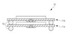
도 1은 종래 기술에 따른 적층 패키지(10)의 한 예를 개략적으로 도시한 단면도로서, 볼 그리드 어레이(이하, BGA라 함) 유형의 단품 패키지를 패키지 적층 방식으로 적층한 구조를 나타낸다. 예시된 바와 같이, 패키지 적층 방식을 이용한 종래의 BGA 적층 패키지(10)는 단품 패키지(11a, 11b)의 가장자리에 위치하는 솔더 볼(12, solder ball)을 통하여 아래위 패키지(11a, 11b)간 적층을 구현하는 것이 일반적이다.1 is a cross-sectional view schematically showing an example of a laminated
종래의 적층 패키지(10)는 다음과 같은 문제점들을 가지고 있다. 도 2는 종래의 적층 패키지(10)에서 발생하는 불량 유형을 도시하고 있다.The conventional laminated
첫째, 단품 패키지(11a, 11b) 자체의 구조적 원인 때문에 종종 패키지 휨(warpage)이 발생하며, 이로 인한 공정 불량, 신뢰성 저하 등의 문제가 발생한다. 부연하자면, 단품 패키지(11a, 11b)는 반도체 칩(13)의 한쪽 면에 배선기판(14)이 부착되는 구조이다. 즉, 구조 및 재질면에서 상하 비대칭을 이루기 때문에, 열을 수반한 각종 공정 중에 열팽창 계수 차이에 따른 휨이 발생한다. 패키지(11a, 11b)의 휨 현상은 솔더 볼(12)을 이용한 적층 공정의 불량(21)을 초래할 수 있고, 적층 후에도 솔더 접합의 깨짐(22, solder joint crack)과 같은 신뢰성 저하의 원인이 된다.First, package warpage often occurs due to the structural causes of the single-
둘째, 종래의 적층 패키지(10)는 반도체 칩(13)의 뒷면이 외부로 노출되는 구조이기 때문에, 외부의 충격에 의하여 반도체 칩(13)이 깨지는 불량(23)이 발생할 수 있다.Second, since the back surface of the
셋째, 일반적인 BGA 패키지는 표준 볼 레이아웃(standard ball layout)이 어레이(array) 형태로 구성된다. 따라서 종래 기술과 같이 동종의 패키지들을 적층할 때 맨 하단의 패키지(11a)는 표준 볼 레이아웃에서 벗어나는 경우가 많다. 이를 배제하기 위하여 맨 하단의 패키지(11a)를 표준 볼 레이아웃으로 구성하면, 상단의 패키지(11b)와 서로 다른 이종 패키지끼리의 적층이 되어 수율 감소를 유발할 수 있다.Third, in a typical BGA package, a standard ball layout is configured in an array form. Therefore, when stacking packages of the same type as in the prior art, the
본 발명의 목적은 패키지 휨 및 그로 인한 적층 불량, 솔더 접합 깨짐 등을 방지할 수 있는 구조의 적층 패키지를 제공하고자 하는 것이다.An object of the present invention is to provide a laminated package having a structure capable of preventing the package warpage and resulting lamination failure, solder joint breakage.
본 발명의 다른 목적은 외부 충격으로 인한 반도체 칩의 깨짐 불량을 방지할 수 있는 구조의 적층 패키지를 제공하기 위한 것이다.Another object of the present invention is to provide a stack package having a structure capable of preventing a broken chip of a semiconductor chip due to an external impact.
본 발명의 또 다른 목적은 표준 볼 레이아웃을 사용하는 패키지끼리의 적층이 가능한 적층 패키지를 제공하기 위한 것이다.Still another object of the present invention is to provide a laminated package capable of laminating packages using a standard ball layout.
이러한 목적들을 달성하기 위하여, 본 발명은 반도체 칩의 아래위에 각각 배선기판이 배치되는 상하 대칭 구조의 적층 패키지를 제공한다.In order to achieve these objects, the present invention provides a stack package having a vertically symmetrical structure in which a wiring board is disposed above and below a semiconductor chip.
본 발명에 따른 적층 패키지는 제1 단품 패키지 및 그 위에 적층된 제2 단품 패키지를 포함하여 구성되며, 각각의 단품 패키지는 활성면과 그 반대쪽인 비활성면을 구비하는 반도체 칩과, 반도체 칩의 활성면 쪽에 위치하는 제1 배선기판과 반도체 칩의 비활성면 쪽에 위치하는 제2 배선기판을 포함한다. 또한, 각각의 단품 패키지는 반도체 칩과 제1 배선기판을 전기적으로 연결하는 제1 내부연결 수단과, 제1 배선기판과 제2 배선기판을 전기적으로 연결하는 제2 내부연결 수단과, 제1 배선기판에 형성되는 외부접속 수단을 더 포함한다. 제2 단품 패키지의 제1 배선기판에 형성된 외부접속 수단은 제1 단품 패키지의 제2 배선기판과 접속된다.The laminated package according to the present invention comprises a first single package and a second single package stacked thereon, each single package having a semiconductor chip having an inactive surface opposite to the active surface, and an active of the semiconductor chip. The first wiring board is located on the surface side and the second wiring board is located on the non-active side of the semiconductor chip. In addition, each single package includes first internal connecting means for electrically connecting the semiconductor chip and the first wiring board, second internal connecting means for electrically connecting the first wiring board and the second wiring board, and the first wiring. It further includes an external connection means formed on the substrate. The external connection means formed on the first wiring board of the second single piece package is connected to the second wiring board of the first single piece package.
본 발명에 따른 적층 패키지에 있어서, 반도체 칩은 활성면에 형성된 복수개의 칩 패드를 구비할 수 있다. 제1 내부연결 수단은 복수개의 제1 본딩 와이어일 수 있고, 제1 배선기판은 칩 부착면의 반대쪽 면에 형성되는 복수개의 제1 본딩 패드를 구비할 수 있다. 이 때, 제1 본딩 와이어는 칩 패드와 제1 본딩 패드를 서로 연결한다.In the stacked package according to the present invention, the semiconductor chip may include a plurality of chip pads formed on the active surface. The first internal connection means may be a plurality of first bonding wires, and the first wiring board may include a plurality of first bonding pads formed on a surface opposite to the chip attaching surface. In this case, the first bonding wire connects the chip pad and the first bonding pad to each other.
칩 패드는 활성면의 중앙을 따라 형성될 수 있고, 제1 배선기판은 칩 패드와 대응하여 중앙을 따라 형성된 홈을 구비할 수 있다. 또한, 각각의 단품 패키지는 제1 본딩 와이어를 덮는 제1 몰딩 수지를 더 포함할 수 있다.The chip pad may be formed along the center of the active surface, and the first wiring board may have a groove formed along the center to correspond to the chip pad. In addition, each one piece package may further include a first molding resin covering the first bonding wire.
제2 내부연결 수단은 복수개의 제2 본딩 와이어일 수 있다. 또한, 제1 배선기판은 칩 부착면에 형성되는 복수개의 제2 본딩 패드를 구비할 수 있고, 제2 배선기판은 칩 부착면의 반대쪽 면에 형성되는 복수개의 제3 본딩 패드를 구비할 수 있다. 이 때, 제2 본딩 와이어는 제2 본딩 패드와 제3 본딩 패드를 서로 연결한다.The second interconnection means may be a plurality of second bonding wires. In addition, the first wiring board may include a plurality of second bonding pads formed on the chip attaching surface, and the second wiring board may include a plurality of third bonding pads formed on the opposite side of the chip attaching surface. . In this case, the second bonding wire connects the second bonding pad and the third bonding pad to each other.
제1 배선기판은 제2 배선기판보다 크기가 큰 것이 바람직하다. 또한, 각각의 단품 패키지는 제2 본딩 와이어를 덮는 제2 몰딩 수지를 더 포함할 수 있다.Preferably, the first wiring board is larger in size than the second wiring board. In addition, each single package may further include a second molding resin covering the second bonding wire.
본 발명의 적층 패키지에 있어서, 외부접속 수단은 복수개의 솔더 볼일 수 있다. 제1 단품 패키지의 솔더 볼과 제2 단품 패키지의 솔더 볼은 서로 동일한 볼 레이아웃을 가지는 것이 바람직하다.In the laminated package of the present invention, the external connection means may be a plurality of solder balls. It is preferable that the solder balls of the first unit package and the solder balls of the second unit package have the same ball layout.
제1 배선기판은 칩 부착면의 반대쪽 면에 형성되는 복수개의 제1 볼 랜드를 구비할 수 있고, 이 때 솔더 볼은 제1 볼 랜드에 형성된다. 또한, 제2 배선기판은 칩 부착면의 반대쪽 면에 형성되는 복수개의 제2 볼 랜드를 구비할 수 있고, 이 때 제2 단품 패키지의 솔더 볼은 제1 단품 패키지의 제2 볼 랜드에 접속된다.The first wiring board may include a plurality of first ball lands formed on the opposite side of the chip attaching surface, wherein the solder balls are formed on the first ball lands. In addition, the second wiring board may include a plurality of second ball lands formed on the opposite side of the chip attaching surface, wherein the solder balls of the second single piece package are connected to the second ball lands of the first single piece package. .
본 발명의 적층 패키지는 반도체 칩의 활성면과 제1 배선기판의 칩 부착면 사이에 개재되는 제1 접착층을 더 포함할 수 있고, 반도체 칩의 비활성면과 제2 배선기판의 칩 부착면 사이에 개재되는 제2 접착층을 더 포함할 수 있다.The multilayer package of the present invention may further include a first adhesive layer interposed between the active surface of the semiconductor chip and the chip attaching surface of the first wiring board, and between the inactive surface of the semiconductor chip and the chip attaching surface of the second wiring board. It may further include a second adhesive layer interposed.
이하, 첨부 도면을 참조하여 본 발명의 실시예를 보다 상세하게 설명하고자 한다.Hereinafter, with reference to the accompanying drawings will be described in detail an embodiment of the present invention.
여기에 설명되는 실시예는 본 발명이 속하는 기술 분야의 당업자들이 본 발명을 충분히 실시할 수 있도록 예시되는 것이지, 본 발명의 범위를 제한하고자 하는 것은 아니다. 실시예를 설명함에 있어, 일부 구조나 제조 공정에 대해서는 그 설명을 생략하거나 도면의 도시를 생략한다. 이는 본 발명의 특징적 구성을 보다 명확하게 보여주기 위한 것이다. 마찬가지의 이유로 도면에 도시된 일부 구성요소들은 때론 과장되게 때론 개략적으로 나타내었고, 각 구성요소의 크기가 실제 크기를 전적으로 반영하는 것은 아니다.The embodiments described herein are illustrated to enable those skilled in the art to which the present invention pertains enough to implement the present invention, but are not intended to limit the scope of the present invention. In describing the embodiments, the description of some structures and manufacturing processes will be omitted or omitted from the drawings. This is to more clearly show the characteristic configuration of the present invention. For the same reason, some of the components shown in the drawings are sometimes exaggerated, sometimes schematically, and the size of each component does not entirely reflect the actual size.
실시예Example
도 3은 본 발명의 실시예에 따른 적층 패키지(30)의 단면도이다.3 is a cross-sectional view of a
도 3을 참조하면, 적층 패키지(30)는 아래쪽에 위치하는 제1 단품 패키지(31a, 이하 하부 패키지)와 위쪽에 위치하는 제2 단품 패키지(31b, 이하 상부 패키지)를 포함하여 구성된다. 이해를 돕기 위해 본 실시예는 두 개의 단품 패키지(31a, 31b) 만으로 이루어지는 적층 패키지(30)를 예로 들었으나, 본 발명이 이에 한정되는 것은 아니다. 상부 패키지(31b)가 하부 패키지(31a) 위에 적층되는 본 실시예의 방식을 따라 제3, 제4, ... 패키지들이 상부 패키지(31b) 위에 더 적층될 수 있음은 물론이다.Referring to FIG. 3, the
하부 패키지(31a)와 상부 패키지(31b)는 동일한 구조를 가진다. 각각의 단품 패키지(31a, 31b)는 활성면과 그 반대쪽인 비활성면을 구비하는 반도체 칩(33a, 33b)을 포함한다. 반도체 칩(33a, 33b)의 활성면 쪽에는 제1 배선기판(34a, 34b, 이하 하부 배선기판)이 위치하며, 비활성면 쪽에는 제2 배선기판(35a, 35b, 이하 상부 배선기판)이 위치한다. 반도체 칩(33a, 33b)과 배선 기판(34a, 34b, 35a, 35b)은 그 사이에 개재된 접착층(36a, 36b)을 통하여 서로 접합된다. 반도체 칩(33a, 33b)은 예컨대 메모리 칩이며, 상하부 배선기판(34a, 34b, 35a, 35b)은 예컨대 인쇄회로기판(PCB)이다. 접착층(36a, 36b)은 액상으로 도포되어 경화된 접착제 또는 테이프 형태로 부착된 접착제이다.The
반도체 칩(33a, 33b)의 아래위에 각각 배선기판(34a, 34b, 35a, 35b)이 배치되므로, 각각의 단품 패키지(31a, 31b)는 구조 및 재질면에서 상하 대칭이 된다. 따라서 소재간 열팽창 계수 차이에 따른 패키지 휨 현상이 최소화될 수 있는 장점이 있다.Since the
각각의 단품 패키지(31a, 31b)는 내부연결 수단(37a, 37b)과 외부접속 수단(32a, 32b)을 더 포함한다. 내부연결 수단(37a, 37b) 중에서 반도체 칩(33a, 33b)과 하부 배선기판(34a, 34b)을 전기적으로 연결하는 것을 제1 내부연결 수단이라 칭하고, 상하부 배선기판(34a, 34b, 35a, 35b)을 전기적으로 연결하는 것을 제2 내부연결 수단이라 칭한다. 외부접속 수단(32a, 32b)은 하부 배선기판(34a, 34b)에 형성된다. 특히, 하부 패키지(31a)의 외부접속 수단(32a)은 적층 패키지(30)의 최종 단자로서, 적층 패키지(30)가 외부 기판에 실장될 때 기계적, 전기적 접속 수단 이 된다. 한편, 상부 패키지(31b)의 외부접속 수단(32b)은 하부 패키지(31a)의 상부 배선기판(35a)과 기계적, 전기적으로 접속된다.Each
내부연결 수단(37a, 37b)은 예컨대 본딩 와이어(bonding wire)이고, 외부접속 수단(32a, 32b)은 예컨대 솔더 볼(solder ball)이다. 그러나 본 발명이 반드시 이에 한정되는 것은 아니다.The internal connecting
반도체 칩(33a, 33b)은 활성면에 형성된 복수개의 칩 패드(chip pad, 도시되지 않음)를 구비한다. 칩 패드는 활성면의 중앙을 따라 형성되는 것이 바람직하지만, 반드시 이에 한정되는 것은 아니다. 하부 배선기판(34a, 34b)은 칩 패드와 대응하여 중앙을 따라 형성된 홈을 구비하며, 칩 부착면의 반대쪽 면에 형성된 복수개의 제1 본딩 패드(도 4의 41, bonding pad)를 구비한다. 따라서 본딩 와이어(37a, 37b)는 홈을 통하여 칩 패드와 제1 본딩 패드를 서로 연결할 수 있다. 이 본딩 와이어(37a, 37b)는 몰딩 수지(38a, 38b, molding resin)로 덮여 외부로부터 보호된다.The
도 4는 본 발명의 실시예에 따른 적층 패키지에 사용되는 단품 패키지 내부의 상하 배선기판(34a, 35a)간 연결 방식을 도시한 사시도이다.4 is a perspective view illustrating a connection method between upper and
도 4를 참조하면, 하부 배선기판(34a)은 칩 부착면의 반대쪽 면에 형성되는 제1 본딩 패드(41)와, 칩 부착면에 형성되는 제2 본딩 패드(42)를 구비한다. 또한, 상부 배선기판(35a)은 칩 부착면의 반대쪽 면에 형성되는 제3 본딩 패드(43)를 구비한다. 도 3을 참조하여 전술한 바와 같이, 제1 본딩 패드(41)는 본딩 와이어를 통하여 반도체 칩의 칩 패드에 연결된다. 도 4 및 도 3에 도시된 바와 같이, 제2 본딩 패드(42)와 제3 본딩 패드(43)는 다른 본딩 와이어(37a)를 통하여 서로 연결된다. 따라서 하부 배선기판(34a)은 상부 배선기판(35a)보다 크기가 큰 것이 바람직하다. 제2, 제3 본딩 패드(42, 43)를 연결하는 본딩 와이어(37a) 또한 도 3에 도시된 바와 같이 몰딩 수지(38a)로 덮여 보호된다.Referring to FIG. 4, the
상하부 배선기판(34a, 35a)은 볼 랜드(44, 45, ball land) 및 비아(46, via)를 더 포함한다. 구체적으로, 하부 배선기판(34a)은 칩 부착면의 반대쪽 면에 형성되는 제1 볼 랜드(44)를 구비하며, 상부 배선기판(35a)은 칩 부착면의 반대쪽 면에 형성되는 제2 볼 랜드(45)를 구비한다. 또한, 하부 배선기판(34a)은 제2 본딩 패드(42)와 제1 볼 랜드(44)를 연결하는 비아(46)를 구비한다. 제1 볼 랜드(44)는 각 단품 패키지(31a, 31b)의 솔더 볼(32a, 32b)이 단품 패키지 제조 공정에서 형성되는 자리이고, 제2 볼 랜드(45)는 단품 패키지 적층 공정에서 상부쪽 단품 패키지(31b)의 솔더 볼(32b)이 접속되는 자리이다.The upper and
한편, 하부 패키지(31a)의 솔더 볼(32a)과 상부 패키지(31b)의 솔더 볼(32b)은 서로 동일한 볼 레이아웃을 가지도록 한다. 칩 선택 핀(chip select pin) 또는 클럭 작동 핀(clock enable pin) 등은 각 단품 패키지(31a, 31b)에 따로 연결되어야 하지만, 본 발명이 속하는 기술 분야에 잘 알려진 바와 같이 배선기판(34a, 34b,35a,35b) 내부의 배선 설계를 적절하게 행함으로써 적층된 모든 단품 패키지들이 서로 동일한 표준 볼 레이아웃을 가지도록 할 수 있다.Meanwhile, the
이상 설명한 적층 패키지는 다음과 같은 방법으로 제조할 수 있다. 도 5a 내지 도 5e는 본 발명의 실시예에 따른 적층 패키지의 제조 방법을 도시한 단면도이 다.The laminated package described above can be manufactured by the following method. 5A to 5E are cross-sectional views illustrating a method of manufacturing a laminated package according to an embodiment of the present invention.
먼저, 도 5a에 도시된 바와 같이, 상부 배선기판(35a)에 반도체 칩(33a)을 부착한다. 이 때 이용되는 접착층(36a)은 상부 배선기판(35a)의 칩 부착면에 접착제를 도포하거나, 반도체 칩(33a)의 비활성면에 접착 테이프를 부착하여 형성할 수 있다.First, as shown in FIG. 5A, the
이어서, 도 5b에 도시된 바와 같이, 하부 배선기판(34a)에 반도체 칩(33a)을 부착한다. 이 때 이용되는 접착층(36a)은 하부 배선기판(34a)에 접착제를 도포하거나 접착 테이프를 부착하여 형성할 수 있다.Subsequently, as shown in FIG. 5B, the
이와 같이 반도체 칩(33a)의 상하부에 각각 배선기판(34a, 35a)을 부착하는 칩 부착 공정을 진행한 후, 도 5c에 도시된 바와 같이, 와이어 본딩 공정을 진행한다. 본딩 와이어(37a)는 반도체 칩(33a)과 하부 배선기판(34a)을 전기적으로 연결하며, 상하부 배선기판(34a, 35a)을 전기적으로 연결한다. 와이어 본딩은 일반적인 와이어 본딩 방식 또는 범프 리버스 본딩(bump reverse bonding) 방식 등이 가능하다.As described above, after the chip attaching process of attaching the
이어서, 도 5d에 도시된 바와 같이, 몰딩 공정과 솔더 볼 형성 공정을 진행한다. 몰딩 공정은 본딩 와이어(37a)를 보호하기 위한 것으로 에폭시 계통의 몰딩 수지(38a)로 본딩 와이어(37a)를 덮는 공정이며, 솔더 볼 형성 공정은 각 배선기판(34a, 35a)의 볼 랜드에 솔더 볼(32a)을 형성하는 공정이다.Subsequently, as shown in FIG. 5D, a molding process and a solder ball forming process are performed. The molding process is to protect the
이상과 같이 단품 패키지의 제조 공정이 완료되면, 도 5e에 도시된 바와 같이, 하부 패키지(31a) 위에 상부 패키지(31b)를 적층하여 적층 패키지(30)를 제조 한다. 이 때, 상부 패키지(31b)의 솔더 볼(32b)이 하부 패키지(31a)의 상부 배선기판(35a)에 부착됨으로써, 상하부 패키지(31a, 31b)간 기계적, 전기적 연결이 이루어진다.When the manufacturing process of the single piece package is completed as described above, as shown in FIG. 5E, the
지금까지 설명한 바와 같이, 본 발명에 따른 적층 패키지는 반도체 칩의 상하부에 각각 배선기판이 위치하므로, 구조 및 재질면에서 실질적으로 대칭 구조를 이루는 단품 패키지를 구현할 수 있다. 따라서 소재간 열팽창 계수 차이로 인하여 발생하는 패키지 휨 현상을 효과적으로 방지할 수 있고, 패키지 휨으로 인하여 초래되는 여러 가지 불량들을 미연에 방지할 수 있다.As described above, in the multilayer package according to the present invention, since wiring boards are positioned at upper and lower portions of the semiconductor chip, a single package having a substantially symmetrical structure in terms of structure and material can be implemented. Therefore, it is possible to effectively prevent the package warpage caused by the difference in thermal expansion coefficient between the materials, and to prevent various defects caused by the package warp in advance.
또한, 본 발명의 적층 패키지는 반도체 칩이 상하부 배선기판과 몰딩 수지로 둘러싸이기 때문에, 외부 충격에 의하여 반도체 칩이 깨지는 불량을 방지할 수 있다.In addition, in the laminated package of the present invention, since the semiconductor chip is surrounded by the upper and lower wiring boards and the molding resin, a defect in which the semiconductor chip is broken due to external impact can be prevented.
아울러, 본 발명의 적층 패키지는 적층을 이루는 단품 패키지들의 구조를 동일하게 구현할 수 있다. 즉, 모든 단품 패키지들이 표준 볼 레이아웃을 가지도록 하여 동종 패키지의 적층 구조를 실현할 수 있으므로, 이종 패키지 적층으로 인한 수율 감소를 방지할 수 있다.In addition, the stack package of the present invention may implement the same structure of the single-piece packages forming the stack. That is, since all the single packages have a standard ball layout, the stacked structure of the homogeneous package can be realized, so that the yield reduction due to the heterogeneous package stacking can be prevented.
Claims (17)
Translated fromKoreanPriority Applications (2)
| Application Number | Priority Date | Filing Date | Title |
|---|---|---|---|
| KR1020050096659AKR100791576B1 (en) | 2005-10-13 | 2005-10-13 | Stacked package of ball grid array type |
| US11/580,080US7642636B2 (en) | 2005-10-13 | 2006-10-13 | Stack package of ball grid array type |
Applications Claiming Priority (1)
| Application Number | Priority Date | Filing Date | Title |
|---|---|---|---|
| KR1020050096659AKR100791576B1 (en) | 2005-10-13 | 2005-10-13 | Stacked package of ball grid array type |
Publications (2)
| Publication Number | Publication Date |
|---|---|
| KR20070095502A KR20070095502A (en) | 2007-10-01 |
| KR100791576B1true KR100791576B1 (en) | 2008-01-03 |
Family
ID=38172499
Family Applications (1)
| Application Number | Title | Priority Date | Filing Date |
|---|---|---|---|
| KR1020050096659AExpired - Fee RelatedKR100791576B1 (en) | 2005-10-13 | 2005-10-13 | Stacked package of ball grid array type |
Country Status (2)
| Country | Link |
|---|---|
| US (1) | US7642636B2 (en) |
| KR (1) | KR100791576B1 (en) |
Families Citing this family (6)
| Publication number | Priority date | Publication date | Assignee | Title |
|---|---|---|---|---|
| SG130055A1 (en) | 2005-08-19 | 2007-03-20 | Micron Technology Inc | Microelectronic devices, stacked microelectronic devices, and methods for manufacturing microelectronic devices |
| SG130066A1 (en)* | 2005-08-26 | 2007-03-20 | Micron Technology Inc | Microelectronic device packages, stacked microelectronic device packages, and methods for manufacturing microelectronic devices |
| US8129225B2 (en)* | 2007-08-10 | 2012-03-06 | Infineon Technologies Ag | Method of manufacturing an integrated circuit module |
| US7911070B2 (en)* | 2008-09-25 | 2011-03-22 | Stats Chippac Ltd. | Integrated circuit packaging system having planar interconnect |
| US9093392B2 (en) | 2010-12-10 | 2015-07-28 | Stats Chippac Ltd. | Integrated circuit packaging system with vertical interconnection and method of manufacture thereof |
| US8432028B2 (en)* | 2011-03-21 | 2013-04-30 | Stats Chippac Ltd. | Integrated circuit packaging system with package-on-package and method of manufacture thereof |
Citations (4)
| Publication number | Priority date | Publication date | Assignee | Title |
|---|---|---|---|---|
| KR20010027266A (en)* | 1999-09-13 | 2001-04-06 | 윤종용 | Stack package |
| KR20050003892A (en)* | 2003-07-04 | 2005-01-12 | 삼성전자주식회사 | Stack package of semiconductor device |
| KR20050020373A (en)* | 2003-08-22 | 2005-03-04 | 삼성전자주식회사 | Stack package made of area array type packages, and manufacturing method thereof |
| KR20050023538A (en)* | 2003-08-28 | 2005-03-10 | 삼성전자주식회사 | Multi chip package having center pads and method for manufacturing the same |
Family Cites Families (9)
| Publication number | Priority date | Publication date | Assignee | Title |
|---|---|---|---|---|
| KR20000056804A (en) | 1999-02-26 | 2000-09-15 | 윤종용 | Stacked type ball grid array package |
| JP3398721B2 (en)* | 1999-05-20 | 2003-04-21 | アムコー テクノロジー コリア インコーポレーティド | Semiconductor package and manufacturing method thereof |
| JP2001077301A (en)* | 1999-08-24 | 2001-03-23 | Amkor Technology Korea Inc | Semiconductor package and its manufacturing method |
| KR100480909B1 (en)* | 2001-12-29 | 2005-04-07 | 주식회사 하이닉스반도체 | method for manufacturing stacked chip package |
| US6686656B1 (en)* | 2003-01-13 | 2004-02-03 | Kingston Technology Corporation | Integrated multi-chip chip scale package |
| TWI311353B (en)* | 2003-04-18 | 2009-06-21 | Advanced Semiconductor Eng | Stacked chip package structure |
| KR100564585B1 (en)* | 2003-11-13 | 2006-03-28 | 삼성전자주식회사 | Dual Stacked BA Packages and Multiple Stacked BA Packages |
| KR100585227B1 (en)* | 2004-03-12 | 2006-06-01 | 삼성전자주식회사 | Semiconductor stack package with improved heat dissipation and memory module using same |
| KR100656587B1 (en)* | 2005-08-08 | 2006-12-13 | 삼성전자주식회사 | Lamination package using lamination board connected via metal post |
- 2005
- 2005-10-13KRKR1020050096659Apatent/KR100791576B1/ennot_activeExpired - Fee Related
- 2006
- 2006-10-13USUS11/580,080patent/US7642636B2/ennot_activeExpired - Fee Related
Patent Citations (4)
| Publication number | Priority date | Publication date | Assignee | Title |
|---|---|---|---|---|
| KR20010027266A (en)* | 1999-09-13 | 2001-04-06 | 윤종용 | Stack package |
| KR20050003892A (en)* | 2003-07-04 | 2005-01-12 | 삼성전자주식회사 | Stack package of semiconductor device |
| KR20050020373A (en)* | 2003-08-22 | 2005-03-04 | 삼성전자주식회사 | Stack package made of area array type packages, and manufacturing method thereof |
| KR20050023538A (en)* | 2003-08-28 | 2005-03-10 | 삼성전자주식회사 | Multi chip package having center pads and method for manufacturing the same |
Also Published As
| Publication number | Publication date |
|---|---|
| US7642636B2 (en) | 2010-01-05 |
| US20070138618A1 (en) | 2007-06-21 |
| KR20070095502A (en) | 2007-10-01 |
Similar Documents
| Publication | Publication Date | Title |
|---|---|---|
| US8766425B2 (en) | Semiconductor device | |
| KR101397203B1 (en) | Semiconductor device | |
| US7679178B2 (en) | Semiconductor package on which a semiconductor device can be stacked and fabrication method thereof | |
| US20090127688A1 (en) | Package-on-package with improved joint reliability | |
| US20070152350A1 (en) | Wiring substrate having variously sized ball pads, semiconductor package having the wiring substrate, and stack package using the semiconductor package | |
| US8288873B2 (en) | Stack package having flexible conductors | |
| JP6100489B2 (en) | Manufacturing method of semiconductor device | |
| US7652361B1 (en) | Land patterns for a semiconductor stacking structure and method therefor | |
| US20130307145A1 (en) | Semiconductor package and method of fabricating the same | |
| US20100044880A1 (en) | Semiconductor device and semiconductor module | |
| US7642636B2 (en) | Stack package of ball grid array type | |
| JP2009026861A (en) | Semiconductor device and manufacturing method thereof | |
| KR20110138788A (en) | Stacked Semiconductor Packages | |
| US7884465B2 (en) | Semiconductor package with passive elements embedded within a semiconductor chip | |
| JP2008277457A (en) | Multilayer semiconductor device and mounting body | |
| TWI357653B (en) | ||
| KR20070051165A (en) | Semiconductor package having pre-solder bumps, laminated package using same, and manufacturing method thereof | |
| JP4654971B2 (en) | Multilayer semiconductor device | |
| KR102862293B1 (en) | Semiconductor package and manufacturing method thereof | |
| KR100256306B1 (en) | Stacked Multi-Chip Modules | |
| JP2005150771A (en) | Wiring board, semiconductor device, and package stack semiconductor device | |
| JP2010056121A (en) | Multilayer semiconductor device | |
| KR100813621B1 (en) | Stacked Semiconductor Device Package | |
| US20090189272A1 (en) | Wafer Level Chip Scale Packages Including Redistribution Substrates and Methods of Fabricating the Same | |
| KR20030045949A (en) | A stack package and a manufacturing method thereof |
Legal Events
| Date | Code | Title | Description |
|---|---|---|---|
| A201 | Request for examination | ||
| PA0109 | Patent application | St.27 status event code:A-0-1-A10-A12-nap-PA0109 | |
| PA0201 | Request for examination | St.27 status event code:A-1-2-D10-D11-exm-PA0201 | |
| D13-X000 | Search requested | St.27 status event code:A-1-2-D10-D13-srh-X000 | |
| D14-X000 | Search report completed | St.27 status event code:A-1-2-D10-D14-srh-X000 | |
| E902 | Notification of reason for refusal | ||
| PE0902 | Notice of grounds for rejection | St.27 status event code:A-1-2-D10-D21-exm-PE0902 | |
| AMND | Amendment | ||
| P11-X000 | Amendment of application requested | St.27 status event code:A-2-2-P10-P11-nap-X000 | |
| P13-X000 | Application amended | St.27 status event code:A-2-2-P10-P13-nap-X000 | |
| E601 | Decision to refuse application | ||
| PE0601 | Decision on rejection of patent | St.27 status event code:N-2-6-B10-B15-exm-PE0601 | |
| AMND | Amendment | ||
| E13-X000 | Pre-grant limitation requested | St.27 status event code:A-2-3-E10-E13-lim-X000 | |
| J201 | Request for trial against refusal decision | ||
| P11-X000 | Amendment of application requested | St.27 status event code:A-2-2-P10-P11-nap-X000 | |
| P13-X000 | Application amended | St.27 status event code:A-2-2-P10-P13-nap-X000 | |
| PJ0201 | Trial against decision of rejection | St.27 status event code:A-3-3-V10-V11-apl-PJ0201 | |
| PB0901 | Examination by re-examination before a trial | St.27 status event code:A-6-3-E10-E12-rex-PB0901 | |
| E801 | Decision on dismissal of amendment | ||
| B601 | Maintenance of original decision after re-examination before a trial | ||
| PB0601 | Maintenance of original decision after re-examination before a trial | St.27 status event code:N-3-6-B10-B17-rex-PB0601 | |
| PG1501 | Laying open of application | St.27 status event code:A-1-1-Q10-Q12-nap-PG1501 | |
| PJ1301 | Trial decision | St.27 status event code:A-3-3-V10-V15-crt-PJ1301 Decision date:20071129 Appeal event data comment text:Appeal Kind Category : Appeal against decision to decline refusal, Appeal Ground Text : 2005 0096659 Appeal request date:20070221 Appellate body name:Patent Examination Board Decision authority category:Office appeal board Decision identifier:2007101002002 | |
| PS0901 | Examination by remand of revocation | St.27 status event code:A-6-3-E10-E12-rex-PS0901 | |
| S901 | Examination by remand of revocation | ||
| GRNO | Decision to grant (after opposition) | ||
| PS0701 | Decision of registration after remand of revocation | St.27 status event code:A-3-4-F10-F13-rex-PS0701 | |
| GRNT | Written decision to grant | ||
| PR0701 | Registration of establishment | St.27 status event code:A-2-4-F10-F11-exm-PR0701 | |
| PR1002 | Payment of registration fee | St.27 status event code:A-2-2-U10-U11-oth-PR1002 Fee payment year number:1 | |
| PG1601 | Publication of registration | St.27 status event code:A-4-4-Q10-Q13-nap-PG1601 | |
| G170 | Re-publication after modification of scope of protection [patent] | ||
| PG1701 | Publication of correction | St.27 status event code:A-5-5-P10-P19-oth-PG1701 Patent document republication publication date:20080411 Republication note text:Request for Correction Notice (Document Request) Gazette number:1007915760000 Gazette reference publication date:20080103 | |
| PR1001 | Payment of annual fee | St.27 status event code:A-4-4-U10-U11-oth-PR1001 Fee payment year number:4 | |
| FPAY | Annual fee payment | Payment date:20111129 Year of fee payment:5 | |
| PR1001 | Payment of annual fee | St.27 status event code:A-4-4-U10-U11-oth-PR1001 Fee payment year number:5 | |
| R18-X000 | Changes to party contact information recorded | St.27 status event code:A-5-5-R10-R18-oth-X000 | |
| LAPS | Lapse due to unpaid annual fee | ||
| PC1903 | Unpaid annual fee | St.27 status event code:A-4-4-U10-U13-oth-PC1903 Not in force date:20121228 Payment event data comment text:Termination Category : DEFAULT_OF_REGISTRATION_FEE | |
| PC1903 | Unpaid annual fee | St.27 status event code:N-4-6-H10-H13-oth-PC1903 Ip right cessation event data comment text:Termination Category : DEFAULT_OF_REGISTRATION_FEE Not in force date:20121228 |