KR100790982B1 - A method of correcting the reset signal level of an active pixel of an image sensor and an image sensor for correcting the reset signal level of an active pixel using an average value of the reset signal levels of the optical black pixels. - Google Patents
A method of correcting the reset signal level of an active pixel of an image sensor and an image sensor for correcting the reset signal level of an active pixel using an average value of the reset signal levels of the optical black pixels.Download PDFInfo
- Publication number
- KR100790982B1 KR100790982B1KR1020060014246AKR20060014246AKR100790982B1KR 100790982 B1KR100790982 B1KR 100790982B1KR 1020060014246 AKR1020060014246 AKR 1020060014246AKR 20060014246 AKR20060014246 AKR 20060014246AKR 100790982 B1KR100790982 B1KR 100790982B1
- Authority
- KR
- South Korea
- Prior art keywords
- reset signal
- active
- level
- optical black
- signal levels
- Prior art date
- Legal status (The legal status is an assumption and is not a legal conclusion. Google has not performed a legal analysis and makes no representation as to the accuracy of the status listed.)
- Expired - Fee Related
Links
Images


Classifications
- H—ELECTRICITY
- H04—ELECTRIC COMMUNICATION TECHNIQUE
- H04N—PICTORIAL COMMUNICATION, e.g. TELEVISION
- H04N25/00—Circuitry of solid-state image sensors [SSIS]; Control thereof
- H04N25/60—Noise processing, e.g. detecting, correcting, reducing or removing noise
- H04N25/65—Noise processing, e.g. detecting, correcting, reducing or removing noise applied to reset noise, e.g. KTC noise related to CMOS structures by techniques other than CDS
- H—ELECTRICITY
- H04—ELECTRIC COMMUNICATION TECHNIQUE
- H04N—PICTORIAL COMMUNICATION, e.g. TELEVISION
- H04N25/00—Circuitry of solid-state image sensors [SSIS]; Control thereof
- H04N25/60—Noise processing, e.g. detecting, correcting, reducing or removing noise
- H04N25/62—Detection or reduction of noise due to excess charges produced by the exposure, e.g. smear, blooming, ghost image, crosstalk or leakage between pixels
- H04N25/627—Detection or reduction of inverted contrast or eclipsing effects
Landscapes
- Engineering & Computer Science (AREA)
- Multimedia (AREA)
- Signal Processing (AREA)
- Transforming Light Signals Into Electric Signals (AREA)
Abstract
Translated fromKoreanDescription
Translated fromKorean본 발명의 상세한 설명에서 인용되는 도면을 보다 충분히 이해하기 위하여 각 도면의 간단한 설명이 제공된다.BRIEF DESCRIPTION OF THE DRAWINGS In order to better understand the drawings cited in the detailed description of the invention, a brief description of each drawing is provided.
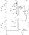
도 1은 본 발명에 따른 옵티컬 블랙 화소들의 리셋 신호 레벨들의 평균값을 이용하여 활성 화소의 리셋 신호 레벨을 보정하는 이미지 센서를 나타내는 블록도이다.1 is a block diagram illustrating an image sensor for correcting a reset signal level of an active pixel by using an average value of reset signal levels of optical black pixels according to the present invention.
도 2는 도 1의 이미지 센서를 상세하게 나타내는 회로도이다.FIG. 2 is a circuit diagram illustrating the image sensor of FIG. 1 in detail.
도 3은 도 2의 리셋 레벨 비교부를 나타내는 회로도이다.3 is a circuit diagram illustrating a reset level comparison unit of FIG. 2.
도 4는 본 발명에 따른 이미지 센서에 포함되는 활성 화소의 리셋 신호 레벨과 일반적인 이미지 센서에 포함되는 활성 화소의 리셋 신호 레벨을 비교한 시뮬레이션 결과를 나타내는 그래프이다.4 is a graph illustrating a simulation result comparing a reset signal level of an active pixel included in an image sensor and a reset signal level of an active pixel included in a general image sensor according to the present invention.
도 5(a)는 일반적인 이미지 센서가 고휘도의 피사체를 촬상한 결과를 나타내 는 도면이다.5A is a diagram illustrating a result of photographing a high-luminance subject by a general image sensor.
도 5(b)는 본 발명에 따른 이미지 센서가 고휘도의 피사체를 촬상한 결과를 나타내는 도면이다.5B is a diagram illustrating a result of capturing a high-luminance subject by the image sensor according to the present invention.
도 6(a)는 도 5(a)의 결과가 나오는 과정을 설명하는 도면이다.FIG. 6 (a) is a diagram for explaining a process of outputting the result of FIG. 5 (a).
도 6(b)는 도 5(b)의 결과가 나오는 과정을 설명하는 도면이다.FIG. 6 (b) is a diagram illustrating a process of outputting the result of FIG. 5 (b).
도 7은 본 발명에 따른 이미지 센서의 활성 화소의 리셋 신호 레벨 보정방법을 나타내는 순서도이다.7 is a flowchart illustrating a method of correcting a reset signal level of an active pixel of an image sensor according to the present invention.
본 발명은 이미지 센서에 관한 것으로써, 특히 옵티컬 블랙 화소들의 리셋 레벨들의 평균값을 이용하여 활성 화소의 리셋 신호 레벨을 보정하는 이미지 센서 및 이미지 센서의 활성 화소의 리셋 신호 레벨 보정방법에 관한 것이다.The present invention relates to an image sensor, and more particularly, to an image sensor for correcting a reset signal level of an active pixel using an average value of reset levels of optical black pixels, and a method of correcting a reset signal level of an active pixel of an image sensor.
이미지 센서가 출력하는 영상 신호 레벨은 리셋 신호 레벨과 포토 다이오드에 저장되는 전하량에 대응되는 신호 레벨의 차이로 결정된다.The image signal level output by the image sensor is determined by the difference between the reset signal level and the signal level corresponding to the amount of charge stored in the photodiode.
그런데, 일반적인 이미지 센서가 고휘도 피사체를 촬상하면, 매우 많은 양의 광전자들이 포토 다이오드로 유입된다. 그에 따라, 포토 다이오드에서는 광전자들이 오버 플로우(overflow)되는 현상이 발생한다. 이 경우, 오버 플로우되는 광전자들은 이미지 센서의 리셋 신호 레벨을 낮춘다.However, when a general image sensor picks up a high-brightness subject, a very large amount of photoelectrons flow into the photodiode. As a result, in the photodiode, the photoelectrons overflow. In this case, the overflowed optoelectronics lower the reset signal level of the image sensor.
그에 따라, 일반적인 이미지 센서가 출력하는 고휘도 피사체의 영상 신호 레 벨은 실제 고휘도 피사체의 영상 신호 레벨보다 낮아지는 문제가 발생한다. 즉, 고휘도 피사체를 촬상한 영상이 실제보다 어둡게 나오거나, 고휘도 피사체를 촬상한 영상의 일부분이 검게 나타나는 문제가 있다. 예를 들어, 일반적인 이미지 센서가 태양을 촬상하는 경우, 태양의 중심 부분이 검게 나타난다.Accordingly, a problem arises in that an image signal level of a high luminance subject output by a general image sensor is lower than an actual image signal level of a high luminance subject. That is, there is a problem in that an image photographing a high brightness subject appears darker than the actual image, or a part of the image photographing a high brightness subject appears black. For example, when a typical image sensor picks up the sun, the central part of the sun appears black.
본 발명이 이루고자 하는 기술적 과제는 옵티컬 블랙 화소들의 리셋 신호 레벨들의 평균값을 이용하여 활성 화소의 리셋 신호 레벨을 보정하는 이미지 센서를 제공하는 데 있다.An object of the present invention is to provide an image sensor for correcting the reset signal level of the active pixel using the average value of the reset signal levels of the optical black pixels.
본 발명에 이루고자 하는 다른 기술적 과제는 옵티컬 블랙 화소들의 리셋 신호 레벨들의 평균값을 이용하여 활성 화소의 리셋 신호 레벨을 보정하는 리셋 신호 레벨 보정방법을 제공하는 데 있다.Another object of the present invention is to provide a reset signal level correction method for correcting a reset signal level of an active pixel by using an average value of reset signal levels of optical black pixels.
상기 기술적 과제를 달성하기 위한 본 발명에 따른 이미지 센서는 활성 화소 어레이, 옵티컬 블랙 화소 어레이 및 리셋 레벨 보정부를 구비한다. 활성 화소 어레이는 복수개의 활성 화소들을 포함한다. 옵티컬 블랙 화소 어레이는 복수개의 옵티컬 블랙 화소들을 포함한다. 리셋 레벨 보정부는 상기 옵티컬 블랙 화소들이 출력하는 옵티컬 블랙 리셋 신호 레벨들의 평균값에 응답하여, 상기 활성 화소들이 출력하는 활성 리셋 신호 레벨들을 보정한다.An image sensor according to the present invention for achieving the above technical problem comprises an active pixel array, an optical black pixel array and a reset level correction unit. The active pixel array includes a plurality of active pixels. The optical black pixel array includes a plurality of optical black pixels. The reset level corrector corrects the active reset signal levels output by the active pixels in response to an average value of the optical black reset signal levels output by the optical black pixels.
상기 리셋 레벨 보정부는 평균 계산부 및 보정 리셋 레벨 출력부를 구비할 수 있다. 상기 평균 계산부는 상기 옵티컬 블랙 리셋 신호 레벨들의 평균값을 계산 하여 출력한다. 상기 보정 리셋 레벨 출력부는 상기 각각의 활성 리셋 신호 레벨과 상기 옵티컬 블랙 리셋 신호 레벨들의 평균값을 비교한 결과에 응답하여, 상기 각각의 활성 리셋 신호 레벨을 보정하여 보정 리셋 신호 레벨로 출력한다.The reset level corrector may include an average calculator and a corrected reset level output unit. The average calculator calculates and outputs an average value of the optical black reset signal levels. The correction reset level output unit corrects each active reset signal level and outputs the correction reset signal level in response to a result of comparing the average value of the respective active reset signal levels and the optical black reset signal levels.
본 발명에 따른 이미지 센서는 상기 활성 리셋 신호 레벨이 상기 옵티컬 블랙 리셋 신호 레벨들의 평균값보다 큰 경우 상기 활성 리셋 신호 레벨을 상기 보정 리셋 신호 레벨 출력하고, 상기 활성 리셋 신호 레벨이 상기 옵티컬 블랙 리셋 신호 레벨들의 평균값보다 작은 경우 소정의 전압 레벨을 상기 보정 리셋 신호 레벨로 출력한다.The image sensor according to the present invention outputs the active reset signal level to the correction reset signal level when the active reset signal level is greater than the average value of the optical black reset signal levels, and wherein the active reset signal level is the optical black reset signal level. If less than the average value of these outputs a predetermined voltage level as the correction reset signal level.
본 발명에 따른 이미지 센서는 제1노드를 더 구비할 수 있다. 상기 각각의 활성 화소는 상기 제1노드로 상기 각각의 활성 리셋 신호 레벨을 출력하고, 상기 보정 리셋 레벨 출력부는 상기 제1노드로 상기 보정 리셋 신호 레벨을 출력할 수 있다.The image sensor according to the present invention may further include a first node. Each active pixel may output the respective active reset signal level to the first node, and the correction reset level output unit may output the correction reset signal level to the first node.
상기 보정 리셋 레벨 출력부는 리셋 레벨 비교부, 제1트랜지스터 및 제2트랜지스터를 구비할 수 있다. 상기 리셋 레벨 비교부는 상기 각각의 활성 리셋 신호 레벨과 상기 옵티컬 블랙 리셋 신호 레벨들의 평균값을 비교하여, 비교 결과를 출력한다. 상기 제1트랜지스터는 상기 비교 결과에 따라 턴-온 또는 턴-오프 되어, 상기 소정의 전압 레벨을 출력한다. 상기 제2트랜지스터는 보정 인에이블 신호에 따라 턴-온 또는 턴-오프 되어, 상기 제1트랜지스터가 출력하는 상기 소정의 전압 레벨을 상기 제1노드로 출력한다.The correction reset level output unit may include a reset level comparison unit, a first transistor, and a second transistor. The reset level comparison unit compares each of the active reset signal levels with the average value of the optical black reset signal levels and outputs a comparison result. The first transistor is turned on or off according to the comparison result, and outputs the predetermined voltage level. The second transistor is turned on or off according to a correction enable signal, and outputs the predetermined voltage level output from the first transistor to the first node.
상기 제1트랜지스터는 상기 활성 리셋 신호 레벨이 상기 옵티컬 블랙 리셋 신호 레벨들의 평균값보다 작은 경우 턴-온 되어 상기 소정의 전압 레벨을 출력하고, 상기 활성 리셋 신호 레벨이 상기 옵티컬 블랙 리셋 신호 레벨들의 평균값보다 큰 경우 턴-오프 될 수 있다.The first transistor is turned on when the active reset signal level is less than the average value of the optical black reset signal levels to output the predetermined voltage level, and the active reset signal level is greater than the average value of the optical black reset signal levels. If large, it can be turned off.
상기 소정의 전압 레벨은 상기 활성 리셋 신호 레벨의 최대값일 수 있다.The predetermined voltage level may be a maximum value of the active reset signal level.
본 발명에 따른 이미지 센서는 오프셋 조정부를 더 구비할 수 있다. 상기 오프셋 조정부는 상기 옵티컬 블랙 리셋 신호 레벨들의 평균값의 레벨을 조정하여 출력한다.The image sensor according to the present invention may further include an offset adjustment unit. The offset adjuster adjusts and outputs a level of an average value of the optical black reset signal levels.
본 발명에 따른 이미지 센서는 CMOS 이미지 센서일 수 있다.The image sensor according to the present invention may be a CMOS image sensor.
상기 다른 기술적 과제를 달성하기 위한 본 발명에 따른 이미지 센서의 활성 화소의 리셋 신호 레벨 보정방법은 복수개의 활성 화소들을 포함하는 활성 화소 어레이 및 복수개의 옵티컬 블랙 화소들을 포함하는 옵티컬 블랙 화소 어레이를 포함한다. 본 발명에 따른 활성 화소의 리셋 신호 레벨 보정방법은 상기 옵티컬 블랙 화소들이 출력하는 옵티컬 블랙 리셋 신호 레벨들의 평균값을 계산하는 단계 및 상기 옵티컬 블랙 리셋 신호 레벨들의 평균값에 응답하여, 상기 활성 화소들이 출력하는 활성 리셋 신호 레벨들을 보정하는 단계를 구비한다.According to another aspect of the present invention, a method of correcting a reset signal level of an active pixel of an image sensor includes an active pixel array including a plurality of active pixels and an optical black pixel array including a plurality of optical black pixels. . According to an exemplary embodiment of the present disclosure, a method of correcting a reset signal level of an active pixel may include calculating an average value of optical black reset signal levels output by the optical black pixels and outputting the active pixels in response to an average value of the optical black reset signal levels. Correcting active reset signal levels.
상기 활성 리셋 신호 레벨들을 보정하는 단계는 상기 각각의 활성 리셋 신호 레벨과 상기 옵티컬 블랙 리셋 신호 레벨들의 평균값을 비교하는 단계 및 상기 비교 결과에 응답하여, 상기 각각의 활성 리셋 신호 레벨을 보정하여 보정 리셋 신호 레벨로 출력하는 단계를 구비할 수 있다.Correcting the active reset signal levels includes comparing the respective average values of the respective active reset signal levels with the optical black reset signal levels and in response to the comparison result, correcting the respective active reset signal levels to correct the reset. Outputting at a signal level.
상기 보정 리셋 신호 레벨로 출력하는 단계는 상기 활성 리셋 신호 레벨이 상기 옵티컬 블랙 리셋 신호 레벨들의 평균값보다 큰 경우 상기 활성 리셋 신호 레벨을 상기 보정 리셋 신호 레벨로 출력하고, 상기 활성 리셋 신호 레벨이 상기 옵티컬 블랙 리셋 신호 레벨들의 평균값보다 작은 경우, 소정의 전압 레벨을 상기 보정 리셋 신호 레벨로 출력하는 것이 바람직하다.The outputting of the correction reset signal level may include outputting the active reset signal level as the correction reset signal level when the active reset signal level is greater than an average value of the optical black reset signal levels, and wherein the active reset signal level is the optical. When smaller than the average value of the black reset signal levels, it is preferable to output a predetermined voltage level as the correction reset signal level.
본 발명과 본 발명의 동작상의 이점 및 본 발명의 실시에 의하여 달성되는 목적을 충분히 이해하기 위해서는 본 발명의 바람직한 실시예를 예시하는 첨부 도면 및 도면에 기재된 내용을 참조하여야 한다.DETAILED DESCRIPTION In order to fully understand the present invention, the operational advantages of the present invention, and the objects achieved by the practice of the present invention, reference should be made to the accompanying drawings which illustrate preferred embodiments of the present invention and the contents described in the drawings.
이하, 첨부한 도면을 참조하여 본 발명의 바람직한 실시예를 설명함으로써, 본 발명을 상세히 설명한다. 각 도면에 제시된 동일한 참조부호는 동일한 부재를 나타낸다.Hereinafter, exemplary embodiments of the present invention will be described in detail with reference to the accompanying drawings. Like reference numerals in the drawings denote like elements.
도 1은 본 발명에 따른 옵티컬 블랙 화소들의 리셋 신호 레벨들의 평균값을 이용하여 활성 화소의 리셋 신호 레벨을 보정하는 이미지 센서를 나타내는 블록도이다.1 is a block diagram illustrating an image sensor for correcting a reset signal level of an active pixel by using an average value of reset signal levels of optical black pixels according to the present invention.
도 1을 참조하면, 본 발명에 따른 이미지 센서(100)는 활성 화소 어레이(110), 옵티컬 블랙 화소 어레이(120) 및 리셋 레벨 보정부(130)를 구비한다. 활성 화소 어레이(110)는 복수개의 활성 화소들(미도시)을 포함한다. 옵티컬 블랙 화소 어레이(120)는 복수개의 옵티컬 블랙 화소들(미도시)을 포함한다. 리셋 레벨 보정부(130)는 옵티컬 블랙 화소들(미도시)이 출력하는 옵티컬 블랙 리셋 신호 레벨들(OBS1~OBSn)의 평균값(OBS_AVG)에 응답하여, 활성 화소들(미도시)이 출력하는 활성 리셋 신호 레벨들(APS1~APSn)을 보정한다.Referring to FIG. 1, the
본 발명에 따른 이미지 센서(100)는 활성 리셋 신호 레벨(APS1~APSn)이 옵티컬 블랙 리셋 신호 레벨들(OBS1~OBSn)의 평균값(OBS_AVG)보다 큰 경우에 활성 리셋 신호 레벨(APS1~APSn)을 출력하고, 활성 리셋 신호 레벨(APS1~APSn)이 옵티컬 블랙 리셋 신호 레벨들(OBS1~OBSn)의 평균값(OBS_AVG)보다 작은 경우에 소정의 전압 레벨을 출력한다.The
즉, 활성 리셋 신호 레벨(APS1~APSn)이 옵티컬 블랙 리셋 신호 레벨들(OBS1~OBSn)의 평균값(OBS_AVG)보다 작은 경우에는, 활성 리셋 신호 레벨(APS1~APSn)이 낮아진 경우이다. 그러므로, 활성 리셋 신호 레벨(APS1~APSn)을 소정의 전압 레벨로 높일 필요가 있다. 여기에서 소정의 전압 레벨은 활성 리셋 신호 레벨(APS1~APSn)이 가질 수 있는 레벨의 최대값일 수 있다.That is, when the active reset signal levels APS1 to APSn are smaller than the average value OBS_AVG of the optical black reset signal levels OBS1 to OBSn, the active reset signal levels APS1 to APSn are lowered. Therefore, it is necessary to raise the active reset signal levels APS1 to APSn to a predetermined voltage level. The predetermined voltage level may be a maximum value of the levels that the active reset signal levels APS1 to APSn may have.
리셋 레벨 보정부(130)는 평균계산부(140) 및 보정 리셋 레벨 출력부(180)를 구비한다. 평균 계산부(140)는 옵티컬 블랙 리셋 신호 레벨들(OBS1~OBSn)의 평균값(OBS_AVG)을 계산하여 출력한다. 보정 리셋 레벨 출력부(180)는 각각의 활성 리셋 신호 레벨(APS1~APSn)과 옵티컬 블랙 리셋 신호 레벨들(OBS1~OBSn)의 평균값(OBS_AVG)을 비교한 결과에 응답하여, 각각의 활성 리셋 신호 레벨(APS1~APSn)을 보정하여 보정 리셋 신호 레벨로 출력한다. 본 발명에 따른 이미지 센서(100)는 오프셋 조정부(160)를 더 구비할 수 있다. 오프셋 조정부(160)는 옵티컬 블랙 리셋 신호 레벨들의 평균값의 레벨을 조정하여 보정 리셋 레벨 출력부(180)로 출력한다.The reset
본 발명에 따른 이미지 센서(100)는 CMOS 이미지 센서일 수 있다.The
도 2는 도 1의 이미지 센서를 상세하게 나타내는 회로도이다.FIG. 2 is a circuit diagram illustrating the image sensor of FIG. 1 in detail.
도 2를 참조하면, 활성 화소 어레이(110)는 복수개의 활성 화소들(110_1~110_n)을 포함한다. 옵티컬 블랙 화소 어레이(120)는 복수개의 옵티컬 블랙 화소들(120_1~120_n)을 포함한다. 보정 리셋 레벨 출력부(180)는 리셋 레벨 비교부(COMP_1), 제1트랜지스터(TR1) 및 제2트랜지스터(TR2)를 구비한다. 오프셋 조정부(160)는 제1버퍼(162), 제2버퍼(166) 및 가변저항(164)을 구비한다.Referring to FIG. 2, the
이하에서 도 2를 참조하여 본 발명에 따른 이미지 센서(100)의 동작이 설명된다. n개의 옵티컬 블랙 화소들(120_1~120_n)은 서로 동일한 구조를 가지고, 서로 동일한 동작을 수행한다. 또한, n개의 활성 화소들(110_1~110_n)은 서로 동일한 구조를 가지고, 서로 동일한 동작을 수행한다. 따라서, 이하에서는 하나의 옵티컬 블랙 화소(120_1) 및 하나의 활성 화소(110_1)만을 이용하여 본 발명에 따른 이미지 센서(100)의 동작을 설명한다.Hereinafter, the operation of the
옵티컬 블랙 화소들(120_1~120_n)은 옵티컬 블랙 리셋 신호들(OBS1~OBSn)을 각각 출력한다. 평균 계산부(140)는 옵티컬 블랙 리셋 신호 레벨들(OBS1~OBSn)을 수신하고, 옵티컬 블랙 리셋 신호 레벨들(OBS1~OBSn)의 평균값(OBS_AVG)을 계산하여 출력한다.The optical black pixels 120_1 to 120_n output optical black reset signals OBS1 to OBSn, respectively. The
오프셋 조정부(160)의 가변저항(164)은 평균값(OBS_AVG)의 레벨을 조정하여 조정 평균값(OBS_CLP)을 출력한다. 여기에서 평균값(OBS_AVG)과 조정 평균값(OBS_CLP)은 서로 동일한 값일 수 있다.The
활성 화소들(110_1~110_n)은 활성 리셋 신호들(APS1~APSn)을 제1노드(NODE1)로 각각 출력한다.The active pixels 110_1 to 110_n respectively output the active reset signals APS1 to APSn to the first node NODE1.
리셋 레벨 비교부(COMP_1)는 조정 평균값(OBS_CLP) 및 활성 리셋 신호(APS1)를 비교하여, 비교 결과를 출력한다. 제1트랜지스터(TR1)는 상기 비교 결과에 따라 턴-온 또는 턴-오프 되어 소정의 전압 레벨(VDD)을 출력한다. 제2트랜지스터(TR2)는 보정 인에이블 신호(CLP_EN)에 따라 턴-온 또는 턴-오프 되어 제1트랜지스터(TR1)가 출력하는 소정의 전압 레벨(VDD)을 제1노드(NODE1)로 출력한다. 보정 인에이블 신호(CLP_EN)는 본 발명에 따른 이미지 센서(100)가 활성 화소의 리셋 레벨을 보정하는 경우에, 논리 하이 레벨로 활성화되는 신호이다.The reset level comparison unit COMP_1 compares the adjustment average value OBS_CLP and the active reset signal APS1 and outputs a comparison result. The first transistor TR1 is turned on or turned off according to the comparison result to output a predetermined voltage level VDD. The second transistor TR2 is turned on or turned off according to the correction enable signal CLP_EN to output a predetermined voltage level VDD output from the first transistor TR1 to the first node NODE1. . The correction enable signal CLP_EN is a signal that is activated to a logic high level when the
우선, 활성 리셋 신호 레벨(APS_1)이 조정 평균값(OBS_CLP) 즉, 옵티컬 블랙 리셋 신호 레벨들의 평균값(OBS_AVG)보다 작은 경우를 살펴본다. 이 경우, 리셋 레벨 비교부(COMP_1)는 논리 하이 레벨을 출력한다. 상기 논리 하이 레벨의 신호는 제1트랜지스터(TR1)의 게이트로 입력된다. 그에 따라, 제1트랜지스터(TR1)는 턴-온 된다. 제1트랜지스터(TR1)가 턴-온 되면, 제2트랜지스터(TR2)의 제1단으로 전원전압(VDD)이 인가된다. 제2트랜지스터(TR2)는 논리 하이 레벨의 보정 인에이블 신호(CLP_EN)에 응답하여 턴-온 된다. 그에 따라, 제2트랜지스터(TR2)는 전원전압(VDD)을 제1노드(NODE1)로 출력한다.First, the case where the active reset signal level APS_1 is smaller than the adjusted average value OBS_CLP, that is, the average value OBS_AVG of the optical black reset signal levels, will be described. In this case, the reset level comparison unit COMP_1 outputs a logic high level. The logic high level signal is input to the gate of the first transistor TR1. Accordingly, the first transistor TR1 is turned on. When the first transistor TR1 is turned on, the power supply voltage VDD is applied to the first terminal of the second transistor TR2. The second transistor TR2 is turned on in response to the logic high level correction enable signal CLP_EN. Accordingly, the second transistor TR2 outputs the power supply voltage VDD to the first node NODE1.
다음으로, 활성 리셋 신호 레벨(APS_1)이 조정 평균값(OBS_CLP) 즉, 옵티컬 블랙 리셋 신호 레벨들의 평균값(OBS_AVG)보다 큰 경우를 살펴본다. 이 경우, 리셋 레벨 비교부(COMP_1)는 논리 로우 레벨을 출력한다. 상기 논리 로우 레벨의 신호는 제1트랜지스터(TR1)의 게이트로 입력된다. 그에 따라, 제1트랜지스터(TR1)는 턴-오프 된다. 제1트랜지스터(TR1)가 턴-오프 되면, 보정 인에이블 신호(CLP_EN)의 논리 레벨에 관계없이 제2트랜지스터(TR2)는 제1노드(NODE1)로 전원전압(VDD)을 출력하지 않는다. 결국, 제1노드(NODE1)에는 활성 리셋 신호 레벨(APS_1)이 인가된다.Next, the case where the active reset signal level APS_1 is greater than the adjusted average value OBS_CLP, that is, the average value OBS_AVG of the optical black reset signal levels, will be described. In this case, the reset level comparison unit COMP_1 outputs a logic low level. The logic low level signal is input to the gate of the first transistor TR1. Accordingly, the first transistor TR1 is turned off. When the first transistor TR1 is turned off, the second transistor TR2 does not output the power supply voltage VDD to the first node NODE1 regardless of the logic level of the correction enable signal CLP_EN. As a result, the active reset signal level APS_1 is applied to the first node NODE1.
따라서, 본 발명에 따른 이미지 센서(100)는 활성 리셋 신호 레벨(APS_1)이 옵티컬 블랙 리셋 신호 레벨들의 평균값(OBS_AVG)보다 큰 경우에는 활성 리셋 신호 레벨(APS_1)을 출력하고, 활성 리셋 신호 레벨(APS_1)이 옵티컬 블랙 리셋 신호 레벨들의 평균값(OBS_AVG)보다 작은 경우에는 전원전압(VDD)을 출력한다.Accordingly, the
도 3은 도 2의 리셋 레벨 비교부(COMP_1)를 나타내는 회로도이다.3 is a circuit diagram illustrating the reset level comparison unit COMP_1 of FIG. 2.
도 3을 참조하면, 리셋 레벨 비교부(COMP_1)는 조정 평균값(OBS_CLP) 및 활성 리셋 신호(APS_1)를 비교하여, 비교 결과를 출력한다. 좀 더 설명하면, 신호(nLAT)가 논리 하이 레벨로 활성화되고, 그에 따라 조정 평균값(OBS_CLP) 및 활성 리셋 신호(APS_1)이 입력된다. 그 다음, 신호(nLAT)가 논리 로우 레벨로 비활성화된다. 그리고, 신호(LATD)가 논리 하이 레벨로 활성화되고, 신호(/LATD)가 논리 로우 레벨로 활성화되어, 조정 평균값(OBS_CLP) 및 활성 리셋 신호(APS_1)가 비교된다.Referring to FIG. 3, the reset level comparison unit COMP_1 compares the adjusted average value OBS_CLP and the active reset signal APS_1 and outputs a comparison result. More specifically, the signal nLAT is activated to a logic high level, and accordingly, the adjustment average value OBS_CLP and the active reset signal APS_1 are input. The signal nLAT is then deactivated to a logic low level. The signal LATD is activated to a logic high level, the signal / LATD is activated to a logic low level, and the adjustment average value OBS_CLP and the active reset signal APS_1 are compared.
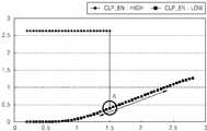
도 4는 본 발명에 따른 이미지 센서에 포함되는 활성 화소의 리셋 신호 레벨과 일반적인 이미지 센서에 포함되는 활성 화소의 리셋 신호 레벨을 비교한 시뮬레이션 결과를 나타내는 그래프이다.4 is a graph illustrating a simulation result comparing a reset signal level of an active pixel included in an image sensor and a reset signal level of an active pixel included in a general image sensor according to the present invention.
도 4를 참조하면, 보정 인에이블 신호(CLP_EN)가 논리 로우 레벨인 경우에는, 즉, 본 발명에 따른 이미지 센서(100)가 활성 화소의 리셋 레벨을 보정하지 않 는 경우에는, 활성 화소의 리셋 레벨이 낮아지는 것을 알 수 있다.Referring to FIG. 4, when the correction enable signal CLP_EN is at a logic low level, that is, when the
반면에, 보정 인에이블 신호(CLP_EN)가 논리 하이 레벨인 경우에는, 즉, 본 발명에 따른 이미지 센서(100)가 활성 화소의 리셋 레벨을 보정하는 경우에는, 활성 화소의 리셋 레벨이 약 2.6V 정도로 보정되는 것을 알 수 있다.On the other hand, when the correction enable signal CLP_EN is at a logic high level, that is, when the
도 5(a)는 일반적인 이미지 센서가 고휘도의 피사체를 촬상한 결과를 나타내는 도면이다.5A is a diagram illustrating a result of photographing a high-luminance subject by a general image sensor.
도 5(b)는 본 발명에 따른 이미지 센서가 고휘도의 피사체를 촬상한 결과를 나타내는 도면이다.5B is a diagram illustrating a result of capturing a high-luminance subject by the image sensor according to the present invention.
도 5(a)를 참조하면, 일반적인 이미지 센서가 고휘도의 피사체를 촬상한 경우, 고휘도 피사체의 영상의 일부분이 검게 나타나는 것을 알 수 있다. 반면에, 도 5(b)를 참조하면, 본 발명에 따른 이미지 센서가 고휘도의 피사체를 촬상한 경우, 고휘도 피사체의 영상이 정상적으로 나타나는 것을 알 수 있다.Referring to FIG. 5A, when a general image sensor photographs a high-luminance subject, a portion of an image of the high-luminance subject appears black. On the other hand, referring to Figure 5 (b), it can be seen that when the image sensor according to the present invention picked up a high-luminance subject, the image of the high-luminance subject appears normally.
도 6(a)는 도 5(a)의 결과가 나오는 과정을 설명하는 도면이다.FIG. 6 (a) is a diagram for explaining a process of outputting the result of FIG. 5 (a).
도 6(b)는 도 5(b)의 결과가 나오는 과정을 설명하는 도면이다.FIG. 6 (b) is a diagram illustrating a process of outputting the result of FIG. 5 (b).
도 6(a)를 참조하면, 일반적인 이미지 센서가 고휘도의 피사체를 촬상한 경우, 활성화소의 리셋 신호 레벨이 낮아진다. 그에 따라, 일반적인 이미지 센서가 출력하는 고휘도 피사체의 영상 신호 레벨은 실제 고휘도 피사체의 영상 신호 레벨보다 낮아진다.Referring to FIG. 6A, when a general image sensor photographs a high-brightness subject, the reset signal level of the activation element is lowered. Accordingly, the video signal level of the high brightness subject output by the general image sensor is lower than the video signal level of the actual high brightness subject.
반면에, 도 6(b)를 참조하면, 본 발명에 따른 이미지 센서가 고휘도의 피사체를 촬상한 경우, 활성화소의 리셋 레벨은 낮아지지 않는다. 그에 따라, 본 발명 에 따른 이미지 센서가 출력하는 고휘도 피사체의 영상 신호 레벨은 실제 고휘도 피사체의 영상 신호 레벨을 그대로 나타낸다.On the other hand, referring to FIG. 6 (b), when the image sensor according to the present invention captures a high brightness subject, the reset level of the activation element is not lowered. Accordingly, the video signal level of the high brightness subject output by the image sensor according to the present invention represents the actual video signal level of the high brightness subject.
도 7은 본 발명에 따른 이미지 센서의 활성 화소의 리셋 신호 레벨 보정방법을 나타내는 순서도이다.7 is a flowchart illustrating a method of correcting a reset signal level of an active pixel of an image sensor according to the present invention.
도 7을 참조하면, 본 발명에 따른 리셋 신호 레벨 보정방법(600)은 복수개의 활성 화소들을 포함하는 활성 화소 어레이 및 복수개의 옵티컬 블랙 화소들을 포함하는 옵티컬 블랙 화소 어레이를 포함하는 이미지 센서의 활성 화소의 리셋 신호 레벨 보정방법이다. 본 발명에 따른 리셋 신호 레벨 보정방법(600)은 옵티컬 블랙 화소들이 출력하는 옵티컬 블랙 리셋 신호 레벨들의 평균값을 계산하는 단계(610) 및 옵티컬 블랙 리셋 신호 레벨들의 평균값에 응답하여, 상기 활성 화소들이 출력하는 활성 리셋 신호 레벨들을 보정하는 단계를 구비한다.Referring to FIG. 7, the reset signal
활성 리셋 신호 레벨들을 보정하는 단계는 각각의 활성 화소가 출력하는 각각의 활성 리셋 레벨과 옵티컬 블랙 리셋 레벨들의 평균값을 비교하는 단계(650) 및 활성 리셋 레벨이 옵티컬 블랙 리셋 레벨들의 평균값보다 큰 경우 활성 리셋 레벨을 출력하고, 활성 리셋 레벨이 옵티컬 블랙 리셋 레벨들의 평균값보다 작은 경우 소정의 전압 레벨을 출력하는 단계(670, 690)를 구비한다.Compensating the active reset signal levels may include comparing the average value of the optical black reset levels with each active reset level output by each active pixel, and active if the active reset level is greater than the average value of the optical black reset levels. Outputting a reset level and outputting a predetermined voltage level if the active reset level is less than the average value of the optical black reset levels (670, 690).
본 발명에 따른 리셋 신호 레벨 보정방법(600)은 옵티컬 블랙 리셋 레벨들의 평균값을 조정하는 단계(630)를 더 구비할 수 있다.The reset signal
본 발명에 따른 리셋 신호 레벨 보정방법(600)은 앞서 설명된 본 발명에 따른 이미지 센서(100)와 기술적 사상이 동일하며, 본 발명에 따른 이미지 센서(100) 의 동작에 대응된다. 그러므로 당업자라면 앞서의 설명으로부터 본 발명에 따른 리셋 신호 레벨 보정방법(600)에 대해서 이해할 수 있을 것이므로, 그에 대한 설명은 생략된다.The reset signal
이상에서와 같이 도면과 명세서에서 최적 실시예가 개시되었다. 여기서 특정한 용어들이 사용되었으나, 이는 단지 본 발명을 설명하기 위한 목적에서 사용된 것이지 의미한정이나 특허청구범위에 기재된 본 발명의 범위를 제한하기 위하여 사용된 것은 아니다. 그러므로 본 기술분야의 통상의 지식을 가진 자라면 이로부터 다양한 변형 및 균등한 타 실시예가 가능하다는 점을 이해할 것이다. 따라서, 본 발명의진정한 기술적 보호범위는 첨부된 특허청구범위의 기술적 사상에 의해 정해져야 할 것이다.As described above, optimal embodiments have been disclosed in the drawings and the specification. Although specific terms have been used herein, they are used only for the purpose of describing the present invention and are not intended to limit the scope of the present invention as defined in the claims or the claims. Therefore, those skilled in the art will understand that various modifications and equivalent other embodiments are possible therefrom. Therefore, the true technical protection scope of the present invention will be defined by the technical spirit of the appended claims.
상술한 바와 같이 본 발명에 따른 이미지 센서는 옵티컬 블랙 화소들 및 활성 화소들의 산포에 관계없이, 안정적인 레벨의 활성 리셋 신호를 출력할 수 있는 장점이 있다.As described above, the image sensor according to the present invention has an advantage of outputting an active reset signal having a stable level regardless of the distribution of the optical black pixels and the active pixels.
Claims (17)
Translated fromKoreanPriority Applications (2)
| Application Number | Priority Date | Filing Date | Title |
|---|---|---|---|
| KR1020060014246AKR100790982B1 (en) | 2006-02-14 | 2006-02-14 | A method of correcting the reset signal level of an active pixel of an image sensor and an image sensor for correcting the reset signal level of an active pixel using an average value of the reset signal levels of the optical black pixels. |
| US11/674,851US20070188641A1 (en) | 2006-02-14 | 2007-02-14 | Method and Image Sensor for Compensating for Reset Signal Levels of Active Pixels |
Applications Claiming Priority (1)
| Application Number | Priority Date | Filing Date | Title |
|---|---|---|---|
| KR1020060014246AKR100790982B1 (en) | 2006-02-14 | 2006-02-14 | A method of correcting the reset signal level of an active pixel of an image sensor and an image sensor for correcting the reset signal level of an active pixel using an average value of the reset signal levels of the optical black pixels. |
Publications (2)
| Publication Number | Publication Date |
|---|---|
| KR20070081937A KR20070081937A (en) | 2007-08-20 |
| KR100790982B1true KR100790982B1 (en) | 2008-01-03 |
Family
ID=38367981
Family Applications (1)
| Application Number | Title | Priority Date | Filing Date |
|---|---|---|---|
| KR1020060014246AExpired - Fee RelatedKR100790982B1 (en) | 2006-02-14 | 2006-02-14 | A method of correcting the reset signal level of an active pixel of an image sensor and an image sensor for correcting the reset signal level of an active pixel using an average value of the reset signal levels of the optical black pixels. |
Country Status (2)
| Country | Link |
|---|---|
| US (1) | US20070188641A1 (en) |
| KR (1) | KR100790982B1 (en) |
Cited By (1)
| Publication number | Priority date | Publication date | Assignee | Title |
|---|---|---|---|---|
| US12395755B2 (en) | 2023-02-21 | 2025-08-19 | Samsung Electronics Co., Ltd. | Image sensor device and operation method thereof with dummy code generator |
Families Citing this family (10)
| Publication number | Priority date | Publication date | Assignee | Title |
|---|---|---|---|---|
| US7916186B2 (en)* | 2005-04-07 | 2011-03-29 | Micron Technology, Inc. | Anti-eclipse circuitry with tracking of floating diffusion reset level |
| KR100744118B1 (en)* | 2005-12-13 | 2007-08-01 | 삼성전자주식회사 | An image sensor having a saturation level detection circuit of the image sensor, a saturation level detection method of the image sensor, and a saturation level detection circuit. |
| TW200919298A (en)* | 2007-08-01 | 2009-05-01 | Silverbrook Res Pty Ltd | Interactive handheld scanner |
| JP5531417B2 (en) | 2009-02-12 | 2014-06-25 | 株式会社ニコン | Solid-state imaging device |
| KR102159261B1 (en)* | 2014-01-21 | 2020-09-23 | 삼성전자 주식회사 | Image sensor capable of correcting output signal |
| KR102443218B1 (en)* | 2016-01-06 | 2022-09-15 | 삼성전자주식회사 | Electronic apparatus and operating method thereof |
| WO2018046617A1 (en)* | 2016-09-07 | 2018-03-15 | Starship Technologies Oü | Method and system for calibrating multiple cameras |
| US10419697B2 (en) | 2016-09-08 | 2019-09-17 | Gvbb Holdings S.A.R.L. | System and method for high dynamic range digital double sampling |
| KR20220122172A (en)* | 2021-02-26 | 2022-09-02 | 에스케이하이닉스 주식회사 | Image sensor and how the image sensor works |
| US12289556B2 (en)* | 2023-04-13 | 2025-04-29 | Semiconductor Components Industries, Llc | Pixel array readout circuitry |
Citations (2)
| Publication number | Priority date | Publication date | Assignee | Title |
|---|---|---|---|---|
| JP2004015712A (en)* | 2002-06-11 | 2004-01-15 | Sony Corp | Solid-state image pickup device and fixed pattern noise removing method therefor |
| KR20050079095A (en)* | 2004-02-04 | 2005-08-09 | 삼성전자주식회사 | Clamp circuit for cmos image sensor |
Family Cites Families (10)
| Publication number | Priority date | Publication date | Assignee | Title |
|---|---|---|---|---|
| US4468704A (en)* | 1982-10-28 | 1984-08-28 | Xerox Corporation | Adaptive thresholder |
| JPH06189130A (en)* | 1992-12-16 | 1994-07-08 | Fuji Xerox Co Ltd | Image processing device |
| US6522355B1 (en)* | 1997-04-10 | 2003-02-18 | Texas Instruments Incorporated | Digital nonuniformity correction for image sensors |
| JP3673620B2 (en)* | 1997-07-18 | 2005-07-20 | キヤノン株式会社 | Photoelectric conversion device |
| US6829007B1 (en)* | 1999-09-03 | 2004-12-07 | Texas Instruments Incorporated | Digital scheme for noise filtering of optical black and offset correction in CCD signal processing |
| US6774942B1 (en)* | 2000-08-17 | 2004-08-10 | Exar Corporation | Black level offset calibration system for CCD image digitizer |
| US6816196B1 (en)* | 2001-06-18 | 2004-11-09 | Ess Technology, Inc. | CMOS imager with quantized correlated double sampling |
| US7259787B2 (en)* | 2003-03-27 | 2007-08-21 | Eastman Kodak Company | Digital black clamp circuit in electronic imaging systems |
| US20050243193A1 (en)* | 2004-04-30 | 2005-11-03 | Bob Gove | Suppression of row-wise noise in an imager |
| US7477298B2 (en)* | 2004-08-30 | 2009-01-13 | Micron Technology, Inc. | Anti-eclipsing circuit for image sensors |
- 2006
- 2006-02-14KRKR1020060014246Apatent/KR100790982B1/ennot_activeExpired - Fee Related
- 2007
- 2007-02-14USUS11/674,851patent/US20070188641A1/ennot_activeAbandoned
Patent Citations (2)
| Publication number | Priority date | Publication date | Assignee | Title |
|---|---|---|---|---|
| JP2004015712A (en)* | 2002-06-11 | 2004-01-15 | Sony Corp | Solid-state image pickup device and fixed pattern noise removing method therefor |
| KR20050079095A (en)* | 2004-02-04 | 2005-08-09 | 삼성전자주식회사 | Clamp circuit for cmos image sensor |
Cited By (1)
| Publication number | Priority date | Publication date | Assignee | Title |
|---|---|---|---|---|
| US12395755B2 (en) | 2023-02-21 | 2025-08-19 | Samsung Electronics Co., Ltd. | Image sensor device and operation method thereof with dummy code generator |
Also Published As
| Publication number | Publication date |
|---|---|
| US20070188641A1 (en) | 2007-08-16 |
| KR20070081937A (en) | 2007-08-20 |
Similar Documents
| Publication | Publication Date | Title |
|---|---|---|
| KR100790982B1 (en) | A method of correcting the reset signal level of an active pixel of an image sensor and an image sensor for correcting the reset signal level of an active pixel using an average value of the reset signal levels of the optical black pixels. | |
| US20220150426A1 (en) | Anti-eclipse circuitry with tracking of floating diffusion reset level | |
| US8035728B2 (en) | Method and apparatus providing rule-based auto exposure technique preserving scene dynamic range | |
| US7379104B2 (en) | Correction apparatus | |
| US9736406B2 (en) | Image capturing apparatus and control method thereof | |
| US20070182845A1 (en) | Auto exposure for digital imagers | |
| US8339482B2 (en) | Image capturing apparatus with correction using optical black areas, control method therefor and program | |
| US20060007331A1 (en) | Image sensor | |
| US7443442B2 (en) | Image apparatus and method for compensating for high and low luminance image portions via exposure control and gamma correction | |
| US20120162467A1 (en) | Image capture device | |
| US20060176519A1 (en) | Black out correction device | |
| US8537254B2 (en) | Image signal processing device and solid-state imaging device | |
| KR100776134B1 (en) | How to adjust image sensor and image brightness distribution | |
| US7903146B2 (en) | Image capturing apparatus with image signal and object luminance detection for exposure control | |
| JP2004282282A (en) | Camera system and camera control method | |
| JP6568368B2 (en) | Imaging apparatus, control method therefor, program, and storage medium | |
| CN108322680B (en) | Temperature self-adaptive black level calibration method and system of image sensor | |
| US7839442B2 (en) | Solid-state image sensing device including reset circuitry and image sensing device including the solid-state image sensing device and method for operating the same | |
| US6867409B2 (en) | Solid-state image sensing device | |
| US20170213322A1 (en) | Image processing device, image processing method, and storage medium | |
| KR100975444B1 (en) | Image sensor with reset voltage compensation | |
| CN114882853B (en) | Exposure time adjustment method, device, adjustment equipment and storage medium | |
| US8625008B2 (en) | Image processing apparatus having luminance-type gamma correction circuit capable of changing nonlinear characteristic, and image processing method therefor | |
| KR101571476B1 (en) | Camera module control device and method | |
| US9549131B2 (en) | Imaging apparatus and imaging method using independently corrected color values |
Legal Events
| Date | Code | Title | Description |
|---|---|---|---|
| A201 | Request for examination | ||
| PA0109 | Patent application | St.27 status event code:A-0-1-A10-A12-nap-PA0109 | |
| PA0201 | Request for examination | St.27 status event code:A-1-2-D10-D11-exm-PA0201 | |
| AMND | Amendment | ||
| P11-X000 | Amendment of application requested | St.27 status event code:A-2-2-P10-P11-nap-X000 | |
| P13-X000 | Application amended | St.27 status event code:A-2-2-P10-P13-nap-X000 | |
| D13-X000 | Search requested | St.27 status event code:A-1-2-D10-D13-srh-X000 | |
| D14-X000 | Search report completed | St.27 status event code:A-1-2-D10-D14-srh-X000 | |
| E902 | Notification of reason for refusal | ||
| PE0902 | Notice of grounds for rejection | St.27 status event code:A-1-2-D10-D21-exm-PE0902 | |
| AMND | Amendment | ||
| P11-X000 | Amendment of application requested | St.27 status event code:A-2-2-P10-P11-nap-X000 | |
| P13-X000 | Application amended | St.27 status event code:A-2-2-P10-P13-nap-X000 | |
| PG1501 | Laying open of application | St.27 status event code:A-1-1-Q10-Q12-nap-PG1501 | |
| E601 | Decision to refuse application | ||
| PE0601 | Decision on rejection of patent | St.27 status event code:N-2-6-B10-B15-exm-PE0601 | |
| J201 | Request for trial against refusal decision | ||
| PJ0201 | Trial against decision of rejection | St.27 status event code:A-3-3-V10-V11-apl-PJ0201 | |
| AMND | Amendment | ||
| E13-X000 | Pre-grant limitation requested | St.27 status event code:A-2-3-E10-E13-lim-X000 | |
| P11-X000 | Amendment of application requested | St.27 status event code:A-2-2-P10-P11-nap-X000 | |
| P13-X000 | Application amended | St.27 status event code:A-2-2-P10-P13-nap-X000 | |
| PB0901 | Examination by re-examination before a trial | St.27 status event code:A-6-3-E10-E12-rex-PB0901 | |
| B701 | Decision to grant | ||
| PB0701 | Decision of registration after re-examination before a trial | St.27 status event code:A-3-4-F10-F13-rex-PB0701 | |
| GRNT | Written decision to grant | ||
| PR0701 | Registration of establishment | St.27 status event code:A-2-4-F10-F11-exm-PR0701 | |
| PR1002 | Payment of registration fee | St.27 status event code:A-2-2-U10-U11-oth-PR1002 Fee payment year number:1 | |
| PG1601 | Publication of registration | St.27 status event code:A-4-4-Q10-Q13-nap-PG1601 | |
| G170 | Re-publication after modification of scope of protection [patent] | ||
| PG1701 | Publication of correction | St.27 status event code:A-5-5-P10-P19-oth-PG1701 Patent document republication publication date:20080411 Republication note text:Request for Correction Notice (Document Request) Gazette number:1007909820000 Gazette reference publication date:20080103 | |
| PR1001 | Payment of annual fee | St.27 status event code:A-4-4-U10-U11-oth-PR1001 Fee payment year number:4 | |
| PR1001 | Payment of annual fee | St.27 status event code:A-4-4-U10-U11-oth-PR1001 Fee payment year number:5 | |
| R18-X000 | Changes to party contact information recorded | St.27 status event code:A-5-5-R10-R18-oth-X000 | |
| FPAY | Annual fee payment | Payment date:20121130 Year of fee payment:6 | |
| PR1001 | Payment of annual fee | St.27 status event code:A-4-4-U10-U11-oth-PR1001 Fee payment year number:6 | |
| FPAY | Annual fee payment | Payment date:20131129 Year of fee payment:7 | |
| PR1001 | Payment of annual fee | St.27 status event code:A-4-4-U10-U11-oth-PR1001 Fee payment year number:7 | |
| LAPS | Lapse due to unpaid annual fee | ||
| PC1903 | Unpaid annual fee | St.27 status event code:A-4-4-U10-U13-oth-PC1903 Not in force date:20141227 Payment event data comment text:Termination Category : DEFAULT_OF_REGISTRATION_FEE | |
| PC1903 | Unpaid annual fee | St.27 status event code:N-4-6-H10-H13-oth-PC1903 Ip right cessation event data comment text:Termination Category : DEFAULT_OF_REGISTRATION_FEE Not in force date:20141227 |