KR100790881B1 - Microfluidic reaction chip and manufacturing method thereof - Google Patents
Microfluidic reaction chip and manufacturing method thereofDownload PDFInfo
- Publication number
- KR100790881B1 KR100790881B1KR1020060063536AKR20060063536AKR100790881B1KR 100790881 B1KR100790881 B1KR 100790881B1KR 1020060063536 AKR1020060063536 AKR 1020060063536AKR 20060063536 AKR20060063536 AKR 20060063536AKR 100790881 B1KR100790881 B1KR 100790881B1
- Authority
- KR
- South Korea
- Prior art keywords
- chamber
- channel
- reaction chip
- microfluidic reaction
- substrate
- Prior art date
- Legal status (The legal status is an assumption and is not a legal conclusion. Google has not performed a legal analysis and makes no representation as to the accuracy of the status listed.)
- Expired - Fee Related
Links
Images


Classifications
- B—PERFORMING OPERATIONS; TRANSPORTING
- B01—PHYSICAL OR CHEMICAL PROCESSES OR APPARATUS IN GENERAL
- B01J—CHEMICAL OR PHYSICAL PROCESSES, e.g. CATALYSIS OR COLLOID CHEMISTRY; THEIR RELEVANT APPARATUS
- B01J19/00—Chemical, physical or physico-chemical processes in general; Their relevant apparatus
- B01J19/0093—Microreactors, e.g. miniaturised or microfabricated reactors
- B—PERFORMING OPERATIONS; TRANSPORTING
- B01—PHYSICAL OR CHEMICAL PROCESSES OR APPARATUS IN GENERAL
- B01L—CHEMICAL OR PHYSICAL LABORATORY APPARATUS FOR GENERAL USE
- B01L3/00—Containers or dishes for laboratory use, e.g. laboratory glassware; Droppers
- B01L3/50—Containers for the purpose of retaining a material to be analysed, e.g. test tubes
- B01L3/502—Containers for the purpose of retaining a material to be analysed, e.g. test tubes with fluid transport, e.g. in multi-compartment structures
- B01L3/5027—Containers for the purpose of retaining a material to be analysed, e.g. test tubes with fluid transport, e.g. in multi-compartment structures by integrated microfluidic structures, i.e. dimensions of channels and chambers are such that surface tension forces are important, e.g. lab-on-a-chip
- B01L3/502707—Containers for the purpose of retaining a material to be analysed, e.g. test tubes with fluid transport, e.g. in multi-compartment structures by integrated microfluidic structures, i.e. dimensions of channels and chambers are such that surface tension forces are important, e.g. lab-on-a-chip characterised by the manufacture of the container or its components
- B—PERFORMING OPERATIONS; TRANSPORTING
- B01—PHYSICAL OR CHEMICAL PROCESSES OR APPARATUS IN GENERAL
- B01L—CHEMICAL OR PHYSICAL LABORATORY APPARATUS FOR GENERAL USE
- B01L3/00—Containers or dishes for laboratory use, e.g. laboratory glassware; Droppers
- B01L3/50—Containers for the purpose of retaining a material to be analysed, e.g. test tubes
- B01L3/502—Containers for the purpose of retaining a material to be analysed, e.g. test tubes with fluid transport, e.g. in multi-compartment structures
- B01L3/5027—Containers for the purpose of retaining a material to be analysed, e.g. test tubes with fluid transport, e.g. in multi-compartment structures by integrated microfluidic structures, i.e. dimensions of channels and chambers are such that surface tension forces are important, e.g. lab-on-a-chip
- B01L3/502746—Containers for the purpose of retaining a material to be analysed, e.g. test tubes with fluid transport, e.g. in multi-compartment structures by integrated microfluidic structures, i.e. dimensions of channels and chambers are such that surface tension forces are important, e.g. lab-on-a-chip characterised by the means for controlling flow resistance, e.g. flow controllers, baffles
- B—PERFORMING OPERATIONS; TRANSPORTING
- B81—MICROSTRUCTURAL TECHNOLOGY
- B81C—PROCESSES OR APPARATUS SPECIALLY ADAPTED FOR THE MANUFACTURE OR TREATMENT OF MICROSTRUCTURAL DEVICES OR SYSTEMS
- B81C1/00—Manufacture or treatment of devices or systems in or on a substrate
- B81C1/00015—Manufacture or treatment of devices or systems in or on a substrate for manufacturing microsystems
- B81C1/00023—Manufacture or treatment of devices or systems in or on a substrate for manufacturing microsystems without movable or flexible elements
- B81C1/00119—Arrangement of basic structures like cavities or channels, e.g. suitable for microfluidic systems
- B—PERFORMING OPERATIONS; TRANSPORTING
- B01—PHYSICAL OR CHEMICAL PROCESSES OR APPARATUS IN GENERAL
- B01J—CHEMICAL OR PHYSICAL PROCESSES, e.g. CATALYSIS OR COLLOID CHEMISTRY; THEIR RELEVANT APPARATUS
- B01J2219/00—Chemical, physical or physico-chemical processes in general; Their relevant apparatus
- B01J2219/00781—Aspects relating to microreactors
- B01J2219/00783—Laminate assemblies, i.e. the reactor comprising a stack of plates
- B—PERFORMING OPERATIONS; TRANSPORTING
- B01—PHYSICAL OR CHEMICAL PROCESSES OR APPARATUS IN GENERAL
- B01J—CHEMICAL OR PHYSICAL PROCESSES, e.g. CATALYSIS OR COLLOID CHEMISTRY; THEIR RELEVANT APPARATUS
- B01J2219/00—Chemical, physical or physico-chemical processes in general; Their relevant apparatus
- B01J2219/00781—Aspects relating to microreactors
- B01J2219/00819—Materials of construction
- B01J2219/00822—Metal
- B—PERFORMING OPERATIONS; TRANSPORTING
- B01—PHYSICAL OR CHEMICAL PROCESSES OR APPARATUS IN GENERAL
- B01J—CHEMICAL OR PHYSICAL PROCESSES, e.g. CATALYSIS OR COLLOID CHEMISTRY; THEIR RELEVANT APPARATUS
- B01J2219/00—Chemical, physical or physico-chemical processes in general; Their relevant apparatus
- B01J2219/00781—Aspects relating to microreactors
- B01J2219/00819—Materials of construction
- B01J2219/00824—Ceramic
- B01J2219/00828—Silicon wafers or plates
- B—PERFORMING OPERATIONS; TRANSPORTING
- B01—PHYSICAL OR CHEMICAL PROCESSES OR APPARATUS IN GENERAL
- B01J—CHEMICAL OR PHYSICAL PROCESSES, e.g. CATALYSIS OR COLLOID CHEMISTRY; THEIR RELEVANT APPARATUS
- B01J2219/00—Chemical, physical or physico-chemical processes in general; Their relevant apparatus
- B01J2219/00781—Aspects relating to microreactors
- B01J2219/00819—Materials of construction
- B01J2219/00833—Plastic
- B—PERFORMING OPERATIONS; TRANSPORTING
- B01—PHYSICAL OR CHEMICAL PROCESSES OR APPARATUS IN GENERAL
- B01J—CHEMICAL OR PHYSICAL PROCESSES, e.g. CATALYSIS OR COLLOID CHEMISTRY; THEIR RELEVANT APPARATUS
- B01J2219/00—Chemical, physical or physico-chemical processes in general; Their relevant apparatus
- B01J2219/00781—Aspects relating to microreactors
- B01J2219/00819—Materials of construction
- B01J2219/00837—Materials of construction comprising coatings other than catalytically active coatings
- B—PERFORMING OPERATIONS; TRANSPORTING
- B01—PHYSICAL OR CHEMICAL PROCESSES OR APPARATUS IN GENERAL
- B01J—CHEMICAL OR PHYSICAL PROCESSES, e.g. CATALYSIS OR COLLOID CHEMISTRY; THEIR RELEVANT APPARATUS
- B01J2219/00—Chemical, physical or physico-chemical processes in general; Their relevant apparatus
- B01J2219/00781—Aspects relating to microreactors
- B01J2219/00873—Heat exchange
- B—PERFORMING OPERATIONS; TRANSPORTING
- B01—PHYSICAL OR CHEMICAL PROCESSES OR APPARATUS IN GENERAL
- B01J—CHEMICAL OR PHYSICAL PROCESSES, e.g. CATALYSIS OR COLLOID CHEMISTRY; THEIR RELEVANT APPARATUS
- B01J2219/00—Chemical, physical or physico-chemical processes in general; Their relevant apparatus
- B01J2219/00781—Aspects relating to microreactors
- B01J2219/0095—Control aspects
- B01J2219/00952—Sensing operations
- B01J2219/00968—Type of sensors
- B01J2219/0097—Optical sensors
- B—PERFORMING OPERATIONS; TRANSPORTING
- B01—PHYSICAL OR CHEMICAL PROCESSES OR APPARATUS IN GENERAL
- B01L—CHEMICAL OR PHYSICAL LABORATORY APPARATUS FOR GENERAL USE
- B01L2200/00—Solutions for specific problems relating to chemical or physical laboratory apparatus
- B01L2200/12—Specific details about manufacturing devices
- B—PERFORMING OPERATIONS; TRANSPORTING
- B01—PHYSICAL OR CHEMICAL PROCESSES OR APPARATUS IN GENERAL
- B01L—CHEMICAL OR PHYSICAL LABORATORY APPARATUS FOR GENERAL USE
- B01L2300/00—Additional constructional details
- B01L2300/08—Geometry, shape and general structure
- B01L2300/0887—Laminated structure
- B—PERFORMING OPERATIONS; TRANSPORTING
- B01—PHYSICAL OR CHEMICAL PROCESSES OR APPARATUS IN GENERAL
- B01L—CHEMICAL OR PHYSICAL LABORATORY APPARATUS FOR GENERAL USE
- B01L2300/00—Additional constructional details
- B01L2300/12—Specific details about materials
- B—PERFORMING OPERATIONS; TRANSPORTING
- B01—PHYSICAL OR CHEMICAL PROCESSES OR APPARATUS IN GENERAL
- B01L—CHEMICAL OR PHYSICAL LABORATORY APPARATUS FOR GENERAL USE
- B01L2300/00—Additional constructional details
- B01L2300/18—Means for temperature control
- B01L2300/1805—Conductive heating, heat from thermostatted solids is conducted to receptacles, e.g. heating plates, blocks
- B—PERFORMING OPERATIONS; TRANSPORTING
- B01—PHYSICAL OR CHEMICAL PROCESSES OR APPARATUS IN GENERAL
- B01L—CHEMICAL OR PHYSICAL LABORATORY APPARATUS FOR GENERAL USE
- B01L3/00—Containers or dishes for laboratory use, e.g. laboratory glassware; Droppers
- B01L3/50—Containers for the purpose of retaining a material to be analysed, e.g. test tubes
- B01L3/502—Containers for the purpose of retaining a material to be analysed, e.g. test tubes with fluid transport, e.g. in multi-compartment structures
- B01L3/5025—Containers for the purpose of retaining a material to be analysed, e.g. test tubes with fluid transport, e.g. in multi-compartment structures for parallel transport of multiple samples
- B—PERFORMING OPERATIONS; TRANSPORTING
- B01—PHYSICAL OR CHEMICAL PROCESSES OR APPARATUS IN GENERAL
- B01L—CHEMICAL OR PHYSICAL LABORATORY APPARATUS FOR GENERAL USE
- B01L7/00—Heating or cooling apparatus; Heat insulating devices
- B01L7/52—Heating or cooling apparatus; Heat insulating devices with provision for submitting samples to a predetermined sequence of different temperatures, e.g. for treating nucleic acid samples
Landscapes
- Chemical & Material Sciences (AREA)
- Health & Medical Sciences (AREA)
- Engineering & Computer Science (AREA)
- Dispersion Chemistry (AREA)
- Chemical Kinetics & Catalysis (AREA)
- Analytical Chemistry (AREA)
- General Health & Medical Sciences (AREA)
- Hematology (AREA)
- Clinical Laboratory Science (AREA)
- Manufacturing & Machinery (AREA)
- Organic Chemistry (AREA)
- Microelectronics & Electronic Packaging (AREA)
- Automatic Analysis And Handling Materials Therefor (AREA)
- Micromachines (AREA)
- Physical Or Chemical Processes And Apparatus (AREA)
Abstract
Translated fromKoreanDescription
Translated fromKorean도 1은 종래의 미세유체 반응칩의 채널에 언더컷(undercut)이 발생된 모습을 도시한 평면도이다.1 is a plan view showing the appearance of an undercut in the channel of a conventional microfluidic reaction chip.
도 2는 본 발명의 바람직한 실시예에 따른 미세유체 반응칩의 평면도이다.2 is a plan view of a microfluidic reaction chip according to a preferred embodiment of the present invention.
도 3은 도 2를 III-III에 따라 절개하여 도시한 단면도이다.FIG. 3 is a cross-sectional view of FIG. 2 taken along line III-III.
도 4a 내지 도 4c는 챔버에 버블이 형성되는 과정이 순차적으로 도시된 컴퓨터 시뮬레이션 자료이다.4A to 4C are computer simulation data sequentially illustrating a process of forming bubbles in a chamber.
도 5a 내지 도 5j는 본 발명의 바람직한 실시예에 따른 미세유체 반응칩을 제조하는 과정을 순차적으로 도시한 단면도이다.5A to 5J are cross-sectional views sequentially illustrating a process of manufacturing a microfluidic reaction chip according to a preferred embodiment of the present invention.
도 6은 비교 대상인 3 종류의 미세유체 반응칩에서 PCR(polymerase chain reaction)을 수행하고 얻어진 형광 검출값을 나타낸 그래프이다.FIG. 6 is a graph illustrating fluorescence detection values obtained by performing polymerase chain reaction (PCR) on three types of microfluidic reaction chips.
<도면의 주요부분에 대한 부호의 설명><Description of the symbols for the main parts of the drawings>
100 ...미세유체 반응칩105 ...하부 기판100 ...
110 ...챔버115 ...상부 기판110
117, 118 ...채널121 ...인렛홀117, 118
122 ...아웃렛홀125 ...소수성 코팅층122 ...
본 발명은 미체유체 공학(microfluidics)에 관한 것으로, 보다 상세하게는 미세유체 반응이 일어나는 미세유체 반응칩과, 이의 제조방법에 관한 것이다.The present invention relates to microfluidics, and more particularly, to a microfluidic reaction chip in which a microfluidic reaction occurs and a method of manufacturing the same.
미세유체 반응 용기는 미량의 유체를 수용하고 그 유체에 예컨대, 중합효소 연쇄반응(PCR: polymerase chain reaction)과 같은 생화학적 반응을 일으켜 상기 유체에 포함된 유전자 발현 양상, 유전자 결함, 단백질 분포 등의 생화학적 특성을 분석할 수 있게 한 용기를 의미한다.Microfluidic reaction vessels contain microfluidic fluids and cause biochemical reactions, such as polymerase chain reactions (PCRs), in such fluids such as gene expression patterns, gene defects, and protein distribution. Refers to a container capable of analyzing biochemical properties.
USP 6,168,948 또는 USP 7,027,638 에는 종래의 미세유체 반응칩의 예가 개시되어 있다. 상기 자료에 개시된 미세유체 반응칩은 복수의 기판을 적층하고 접착하여 만들어지며, 하나의 기판에만 챔버(chamber)와 채널(channel)이 형성되어 있고, 다른 기판에는 챔버 또는 채널이 형성되지 않는다. 이와 같은 미세유체 반응칩은 제조가 비교적 용이하다는 장점은 있으나, 챔버와 채널이 하나의 기판에 형성되어야 하므로, 많은 수의 챔버와 그에 대응하는 채널을 일정한 사이즈(size)의 미세유체 반응칩에 집적하기는 어렵다는 문제점이 있다. 특히, 근래에는 열전도가 우수한 실리콘(Si)이 기판의 재질로 자주 이용되는데, 상기 실리콘(Si) 기판에 습식 에칭(wet etching)에 의해 채널을 형성하면 언더컷(undercut)이 발생될 수 있다. 도 1은 종래의 미세유체 반응칩의 채널 패턴에 언더컷(undercut)이 발생된 모습을 도시한 평면도인데, 이하에서 상기 도 1을 참조하여 언더컷을 설명한다.USP 6,168,948 or USP 7,027,638 discloses examples of conventional microfluidic reaction chips. The microfluidic reaction chip disclosed in the material is made by stacking and adhering a plurality of substrates, and a chamber and a channel are formed in only one substrate, and no chamber or channel is formed in another substrate. Such a microfluidic reaction chip has an advantage of being relatively easy to manufacture, but since a chamber and a channel must be formed on a single substrate, a large number of chambers and corresponding channels are integrated into a microfluidic reaction chip of a predetermined size. There is a problem that it is difficult to do. In particular, recently, silicon (Si) having excellent thermal conductivity is frequently used as a material of a substrate, and undercut may occur when a channel is formed on the silicon (Si) substrate by wet etching. FIG. 1 is a plan view illustrating a state in which an undercut is generated in a channel pattern of a conventional microfluidic reaction chip. Hereinafter, an undercut will be described with reference to FIG. 1.
도 1을 참조하면, 실리콘 기판(10)에 습식 에칭에 의해 채널(15)을 형성하면 실리콘의 결정면에 따른 에칭율(etching rate)의 차이로 인하여 굽어진 부분에서 실선으로 도시된 설계 라인(D)과 가상선으로 도시된 에칭 라인(E)이 달라지게 되는데, 이를 언더컷이라고 한다. 이러한 언더컷은 기판에 굴곡진 부분이 많은 채널을 설계하기 곤란하게 하는 장애 요소가 되므로, 미세유체 반응칩에 챔버와 채널을 집적되게 설계하는데 한계가 있다. 만약, 건식 에칭(dry etching)에 의해 채널을 형성하면 상기한 언더컷은 발생되지 않으나 습식 에칭에 비해 비용이 증대되고, 챔버와 채널 간 에칭 깊이를 차별화하기 위하여 부가적인 공정 단계가 더 필요하게 되어 챔버와 채널을 집적되게 설계하는데 여전히 어려움이 있다.Referring to FIG. 1, when the
본 발명은 상기한 문제점을 해결하기 위한 것으로, 챔버와 채널을 집적되게 설계하기 용이하도록 구조가 개선된 미세유체 반응칩 및, 이의 제조방법을 제공하는 것을 기술적 과제로 한다.The present invention is to solve the above problems, to provide a microfluidic reaction chip having an improved structure to facilitate the design of the chamber and the channel integrated, and to provide a method of manufacturing the same.
상기한 기술적 과제를 달성하기 위하여 본 발명은, 하부 기판; 상기 하부 기판의 상면에, 하면이 대면하여 본딩(bonding)되는 상부 기판; 상기 하부 기판의 상면에 형성된, 유체가 수용되는 적어도 하나 이상의 챔버(chamber); 및, 상기 상부 기판의 하면에 형성된, 상기 챔버에 연결되는 적어도 하나 이상의 채널(channel);을 구비한 것을 특징으로 하는 미세유체 반응칩을 제공한다.The present invention to achieve the above technical problem, the lower substrate; An upper substrate having a lower surface facing and bonded to an upper surface of the lower substrate; At least one chamber formed on an upper surface of the lower substrate to accommodate a fluid; And at least one channel connected to the chamber formed on a lower surface of the upper substrate.
바람직하게는, 상기 하부 기판은 상기 상부 기판에 비하여 상대적으로 열전 도가 클 수 있다.Preferably, the lower substrate may have a greater thermal conductivity than the upper substrate.
바람직하게는, 상기 하부 기판의 재질은 실리콘(Si) 또는 열전도성 금속일 수 있다.Preferably, the material of the lower substrate may be silicon (Si) or a thermally conductive metal.
바람직하게는, 상기 열전도성 금속은 은(Ag), 구리(Cu), 알루미늄(Al), 철(Fe), 및 이들의 합금 중에서 선택된 어느 하나일 수 있다.Preferably, the thermally conductive metal may be any one selected from silver (Ag), copper (Cu), aluminum (Al), iron (Fe), and alloys thereof.
바람직하게는, 상기 상부 기판은 챔버에서의 유체 반응을 형광 검출할 수 있도록 투명할 수 있다.Preferably, the upper substrate may be transparent to fluoresce the fluid reaction in the chamber.
바람직하게는, 상기 상부 기판의 재질은 유리 또는 플라스틱일 수 있다.Preferably, the material of the upper substrate may be glass or plastic.
바람직하게는, 상기 플라스틱은 PMMA(poly methyl meta acrylate), PC(poly carbonate), 및 PDMS(poly dimethyl siloxane) 중에서 선택된 어느 하나일 수 있다.Preferably, the plastic may be any one selected from poly methyl meta acrylate (PMMA), poly carbonate (PC), and poly dimethyl siloxane (PDMS).
바람직하게는, 상기 미세유체 반응칩은 상기 상부 기판에 유체의 유입 및 유출을 위한 인렛홀(inlet hole) 및 아웃렛홀(outlet hole)을 구비할 수 있다.Preferably, the microfluidic reaction chip may include an inlet hole and an outlet hole for inflow and outflow of fluid in the upper substrate.
바람직하게는, 상기 미세유체 반응칩은 상기 챔버 및 상기 채널의 내면에 소수성 물질(hydrophobic material)의 코팅에 의해 형성된 소수성 코팅층을 구비할 수 있다.Preferably, the microfluidic reaction chip may include a hydrophobic coating layer formed by coating a hydrophobic material on the inner surface of the chamber and the channel.
바람직하게는, 상기 소수성 물질은 페렐린(parylene) 계열 또는 테프론(Teflon®) 계열 물질일 수 있다.Preferably, the hydrophobic material may be a parylene-based or Teflon®-based material.
바람직하게는, 상기 소수성 코팅층은 상기 소수성 물질의 화학기상증착(CVD)에 의해 형성된 것일 수 있다.Preferably, the hydrophobic coating layer may be formed by chemical vapor deposition (CVD) of the hydrophobic material.
바람직하게는, 상기 소수성 물질은 상기 챔버 및 채널의 내면에 대하여 직접 코팅될 수 있다.Preferably, the hydrophobic material may be coated directly to the inner surface of the chamber and channel.
삭제delete
바람직하게는, 상기 챔버의 깊이가 채널의 깊이보다 깊을 수 있다.Preferably, the depth of the chamber may be deeper than the depth of the channel.
또한, 본 발명은, 하부 기판의 상면에 유체가 수용되는 적어도 하나 이상의 챔버(chamber)를 형성하는 챔버 형성 단계; 상부 기판의 하면에 유체의 유로가 되는 적어도 하나 이상의 채널(channel)을 형성하는 채널 형성 단계; 및, 상기 챔버와 채널이 연결되도록, 상기 하부 기판의 상면과 상부 기판의 하면을 본딩(bonding)하는 본딩 단계;를 포함하는 것을 특징으로 하는 미세유체 반응칩의 제조방법을 제공한다.In addition, the present invention, the chamber forming step of forming at least one chamber (chamber) for receiving the fluid on the upper surface of the lower substrate; A channel forming step of forming at least one channel that becomes a flow path of the fluid on the lower surface of the upper substrate; And a bonding step of bonding the upper surface of the lower substrate and the lower surface of the upper substrate so that the chamber and the channel are connected to each other.
바람직하게는, 상기 챔버 형성 단계는, 포토리소그래피(photolithography)에 의해 상기 하부 기판의 상면에 챔버가 형성될 자리가 노출된 챔버용 패턴을 형성하는 단계와, 상기 노출된 챔버가 형성될 자리를 에칭(etching)하는 단계와, 상기 챔버용 패턴을 제거하는 단계를 포함할 수 있다.Preferably, the chamber forming step comprises the steps of forming a pattern for the chamber in which the place where the chamber is to be formed is exposed on the upper surface of the lower substrate by photolithography, and etching the place where the exposed chamber is to be formed. (etching) and removing the chamber pattern.
바람직하게는, 상기 채널 형성 단계는, 포토리소그래피에 의해 상기 상부 기판의 하면에 채널이 형성될 자리가 노출된 채널용 패턴을 형성하는 단계와, 상기 노출된 채널이 형성될 자리를 샌드 블라스팅(sand blasting)하는 단계와, 상기 채널용 패턴을 제거하는 단계를 포함할 수 있다.Preferably, the channel forming step may include forming a pattern for a channel where the channel is formed on the bottom surface of the upper substrate by photolithography, and sand blasting the position where the exposed channel is to be formed. blasting) and removing the channel pattern.
바람직하게는, 상기 본딩 단계에서 하부 기판과 상부 기판은 어노딕 본 딩(anodic bonding), 퓨전 본딩(fusion bonding), 접착제 본딩(adhesive bonding), 및 폴리머 본딩(polymer bonding) 중에서 선택된 어느 하나의 본딩 방법에 의해 결합될 수 있다.Preferably, in the bonding step, the lower substrate and the upper substrate may be any one selected from anodical bonding, fusion bonding, adhesive bonding, and polymer bonding. It can be combined by the method.
바람직하게는, 상기 하부 기판의 재질은 실리콘(Si) 또는 열전도성 금속일 수 있다.Preferably, the material of the lower substrate may be silicon (Si) or a thermally conductive metal.
바람직하게는, 상기 열전도성 금속은 은(Ag), 구리(Cu), 알루미늄(Al), 철(Fe), 및 이들의 합금 중에서 선택된 어느 하나일 수 있다.Preferably, the thermally conductive metal may be any one selected from silver (Ag), copper (Cu), aluminum (Al), iron (Fe), and alloys thereof.
바람직하게는, 상기 상부 기판은 챔버에서의 유체 반응을 형광 검출할 수 있도록 투명할 수 있다.Preferably, the upper substrate may be transparent to fluoresce the fluid reaction in the chamber.
바람직하게는, 상기 상부 기판의 재질은 유리 또는 플라스틱일 수 있다.Preferably, the material of the upper substrate may be glass or plastic.
바람직하게는, 상기 플라스틱은 PMMA(poly methyl meta acrylate), PC(poly carbonate), 및 PDMS(poly dimethyl siloxane) 중에서 선택된 어느 하나일 수 있다.Preferably, the plastic may be any one selected from poly methyl meta acrylate (PMMA), poly carbonate (PC), and poly dimethyl siloxane (PDMS).
바람직하게는, 상기 미세유체 반응칩의 제조방법은 상기 하부 기판과 상부 기판을 본딩하기에 앞서서, 상기 상부 기판에 유체의 유입 및 유출을 위한 인렛홀(inlet hole) 및 아웃렛홀(outlet hole)을 형성하는 홀 형성 단계를 더 포함할 수 있다.Preferably, the method of manufacturing the microfluidic reaction chip includes an inlet hole and an outlet hole for inflow and outflow of fluid into the upper substrate prior to bonding the lower substrate and the upper substrate. The method may further include forming a hole.
바람직하게는, 상기 홀 형성 단계는, 포토리소그래피에 의해 상기 상부 기판의 상면에 인렛홀 및 아웃렛홀이 형성될 자리가 노출된 홀(hole)용 패턴을 형성하는 단계와, 상기 노출된 인렛홀 및 아웃렛홀이 형성될 자리를 샌드 블라스팅하는 단계와, 상기 홀용 패턴을 제거하는 단계를 포함할 수 있다.Preferably, the hole forming step comprises the steps of forming a pattern for a hole in which an inlet hole and an outlet hole are formed on the upper surface of the upper substrate by photolithography; Sandblasting a place where the outlet hole is to be formed, and removing the hole pattern.
바람직하게는, 상기 미세유체 반응칩의 제조방법은 상기 챔버 및 상기 채널의 내면에 소수성 물질(hydrophobic material)을 코팅하여 소수성 코팅층을 형성하는 단계를 더 포함할 수 있다.Preferably, the method of manufacturing the microfluidic reaction chip may further include forming a hydrophobic coating layer by coating a hydrophobic material on an inner surface of the chamber and the channel.
바람직하게는, 상기 소수성 물질은 페렐린(parylene) 계열 또는 테프론(Teflon®) 계열 물질일 수 있다.Preferably, the hydrophobic material may be a parylene-based or Teflon®-based material.
바람직하게는, 상기 소수성 물질을 화학기상증착(CVD)에 의해 챔버와 채널의 내면에 증착하여 상기 소수성 코팅층을 형성할 수 있다.Preferably, the hydrophobic material may be deposited on the inner surface of the chamber and the channel by chemical vapor deposition (CVD) to form the hydrophobic coating layer.
바람직하게는, 상기 소수성 물질을 상기 챔버 및 채널의 내면에 대하여 직접 코팅하여 소수성 코팅층을 형성할 수 있다.Preferably, the hydrophobic material may be directly coated on the inner surfaces of the chamber and the channel to form a hydrophobic coating layer.
바람직하게는, 상기 챔버는 상기 채널보다 그 깊이가 더 깊게 형성될 수 있다.Preferably, the chamber may be formed deeper than the channel.
삭제delete
이하, 첨부된 도면을 참조하여 본 발명의 바람직한 실시예에 따른 미세유체 반응칩 및, 이의 제조방법을 상세하게 설명한다.Hereinafter, with reference to the accompanying drawings will be described in detail a microfluidic reaction chip and a method for manufacturing the same according to a preferred embodiment of the present invention.
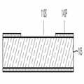
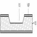
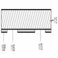
도 2는 본 발명의 바람직한 실시예에 따른 미세유체 반응칩의 평면도이고, 도 3은 도 2를 III-III에 따라 절개하여 도시한 단면도이다.FIG. 2 is a plan view of a microfluidic reaction chip according to a preferred embodiment of the present invention, and FIG. 3 is a cross-sectional view of FIG. 2 taken along line III-III.
도 2 및 도 3을 참조하면, 본 발명의 미세유체 반응칩(100)은 하부 기판(105)과, 상기 하부 기판(105)의 상측에 적층하여 본딩(bonding)된 상부 기 판(115)을 구비한다. 또한, 상기 하부 기판(105)의 상면에 형성된 챔버(chamber, 110)와, 상기 상부 기판(115)의 하면에 형성된 채널(channel, 117, 118)을 구비한다. 상기 하부 기판(105)의 상면과 상부 기판(115)의 하면은 서로 대면하여 본딩되어 있다. 또한, 상기 미세유체 반응칩(100)은 상부 기판(115)에 형성된 인렛홀(inlet hole, 121)과 아웃렛홀(outlet hole, 122)을 구비한다.2 and 3, the
상기 챔버(110)는 유체가 수용되고, 수용된 유체의 생화학 반응이 일어나는 장소로서, 상기 챔버(110)에서 일어난 생화학 반응은 형광 검출법 등의 방법으로 검출될 수 있다. 상기 채널(117, 118)은 유체가 챔버(110)로 유입되는 유로를 형성하는 인렛 채널(inlet channel, 117)과, 유체가 챔버(110)로부터 유출되는 유로를 형성하는 아웃렛 채널(118)로 구분된다. 상기 인렛 채널(117)의 일단은 챔버(110)에 연결되고 타단은 인렛홀(121)에 연결된다. 상기 아웃렛 채널(118)의 일단은 챔버(110)에 연결되고 타단은 아웃렛홀(122)에 연결된다. 상기 인렛홀(121)을 통해 유체가 미세유체 반응칩(100) 내부로 유입되고, 상기 아웃렛홀(122)을 통해 유체가 미세유체 반응칩(100) 외부로 유출된다.The
바람직한 실시예에서 상기 챔버(110)의 깊이(D1)가 채널(117, 118)의 깊이(D2)보다 깊다. 이에 의해, 미세유체 반응칩(100) 내부의 전체 유체 수용 볼륨(volume)에서 챔버(110)가 차지하는 유체 수용 볼륨의 비율이 종래에 비해 증대될 수 있다. 이는 생화학 반응 결과를 검출하는 데 필요한 유체의 최소량이 종래의 경우보다 작아지고, 이에 따라 LOD(limit of detection) 특성이 향상될 수 있음을 의미한다.In a preferred embodiment the depth D1 of the
상기 하부 기판(105)은 PCR 등의 생화학 반응에서 히터(heater)의 열이 챔버(110)에 빨리 전달될 수 있도록 열전도도가 비교적 큰 실리콘(Si) 또는 열전도성 금속 재질의 기판이 바람직하다. 상기 열전도성 금속의 구체적인 예에는 은(Ag), 구리(Cu), 알루미늄(Al), 철(Fe) 및, 상기 금속들의 합금이 포함된다.The
상기 상부 기판(115)은 하부 기판(105)에 비해 열전도도는 작아도 무방하다. 그러나, 챔버(110)에 비해 상대적으로 미세한 폭을 가지며, 굴곡진 라인 형태로 설계되는 채널(117, 118)을 설계 형상대로 정밀하게 가공할 수 있도록 상부 기판(115)은 하부 기판(105)보다 가공성이 우수한 재질로 이루어진 것이 바람직하다. 또한, 상기 상부 기판(115)은 유체의 생화학 반응을 형광 검출법에 의해 검출할 수 있도록 투명한 재질의 기판이 바람직하다. 따라서, 상기 상부 기판(115)의 재질은 유리 또는 플라스틱이 바람직하다. 상기 플라스틱의 구체적 예에는 PMMA(poly methyl meta acrylate), PC(poly carbonate), 및 PDMS(poly dimethyl siloxane)이 포함된다. 도시된 실시예에서 상부 기판(115)은 유리 재질의 기판이 채용되며, 더욱 구체적으로는 상품명 pyrex 7740'인 유리 재질로 된 기판이 채용될 수 있다.The
상기 챔버(110), 인렛 채널(117), 아웃렛 채널(118), 인렛홀(121) 및, 아웃렛홀(122)의 내면에는 소수성 물질(hydrophobic material)이 코팅에 의해 형성된 소수성 코팅층(125)이 마련된다. 실리콘(Si)은 공기중의 산소에 의해 표면이 쉽게 산화하는 특징이 있다. 실리콘 산화물, 즉 SiO2 이 코팅된 표면은 물과의 접촉각(contact angle)이 10 내지 20도인 친수성 표면(hydrophilic surface)이 된다.On the inner surface of the
도 4a 내지 도 4c는 챔버에 버블이 형성되는 과정이 순차적으로 도시된 컴퓨 터 시뮬레이션 자료로서, 유체가 인렛 채널(117)로부터 실리콘(Si) 재질의 기판에 형성된 챔버(110)에 유입되면, SiO2 가 표면에 분포된 챔버 내면을 타고 유체가 흘러 아웃렛 채널(118)로 바로 빠져 나가게 되어, 챔버(110) 내부에 버블(B)이 쉽게 형성될 수 있음을 보여준다. 상기 버블(B)은 챔버(110)에서 유체의 생화학 반응을 검출하기 어렵게 만든다. 따라서, 상기 미세유체 반응칩(100) 내부에 형성된 공간의 내면에는 이러한 버블(B) 형성을 억제하기 위하여 상기한 소수성 코팅층(125)이 형성된다.4A to 4C are computer simulation data sequentially illustrating a process of forming bubbles in a chamber. When fluid flows from the
상기 소수성 코팅층(125)은 페렐린(parylene) 계열 물질 또는 테프론(Teflon®) 계열 물질로 이루어질 수 있다. 도시된 실시예에서 상기 소수성 코팅층(125)은 페렐린으로 이루어져 있으며, 소수성 물질인 페렐린 이합체(dimer)를 화상기상증착(CVD)하여 형성된다. 하부 기판(105)과 상부 기판(115)의 본딩에는 고온 조건 또는 고전압 조건이 요구되므로 본딩 과정 이후에 소수성 코팅층(125)을 형성하는 것이 바람직하다. 화학기상증착 과정에서 페렐린 이합체가 미세한 챔버(117, 118)의 내면에 조밀하게 부착되고, 또한 미세한 챔버(117, 118)를 용이하게 통과할 수 있도록 페렐린 이합체 가운데 입자 크기가 작은 N-타입(type) 페렐린 이합체가 사용되는 것이 바람직하다. 한편, 통상적으로 페렐린 증착에는 실렌(silane) 계열 물질을 부착 촉진자(adhesion promoter)로 사용하나, 본 발명의 바람직한 실시예에서는 이러한 부착 촉진자의 도움 없이 페렐린 계열 물질이 직접 챔버(110), 채널(117, 118), 인렛홀(121) 및, 아웃렛홀(122)의 내면에 증착된다. 그 이유에 대해서는 후술한다.The
도 5a 내지 도 5j는 본 발명의 바람직한 실시예에 따른 미세유체 반응칩을 제조하는 과정을 순차적으로 도시한 단면도로서, 이하에서 상기 도면들을 참조하여 본 발명의 바람직한 실시예에 따른 미세유체 반응칩의 제조방법을 상세하게 설명한다.5A to 5J are cross-sectional views sequentially illustrating a process of manufacturing a microfluidic reaction chip according to a preferred embodiment of the present invention. Hereinafter, a microfluidic reaction chip according to a preferred embodiment of the present invention will be described with reference to the drawings. The manufacturing method will be described in detail.
도 5a 내지 도 5j를 참조하면, 미세유체 반응칩(100)의 제조방법은 크게, 하부 기판(105)에 챔버(110)를 형성하는 챔버 형성 단계(도 5a 내지 5d 참조)와, 상부 기판(115)에 채널(117, 118)을 형성하는 채널 형성 단계(도 5e 및 도 5f 참조)와, 상부 기판(115)에 인렛홀(121)과 아웃렛홀(122)을 형성하는 홀 형성 단계(도 5g 및 도 5h 참조)와, 하부 기판(105)과 상부 기판(115)을 본딩(bonding)하는 본딩 단계(도 5i 참조)와, 소수성 코팅층(125) 형성 단계(도 5j 참조)를 포함한다.5A to 5J, the method of manufacturing the
상기 챔버 형성 단계는, 도 5a 및 도 5b에 순차로 도시된 바와 같이 포토리소그래피(photolithography)에 의해 하부 기판(105)의 상면에 챔버용 패턴(140P)을 형성하는 단계와, 도 5c에 도시된 바와 같이 에칭(etching)하여 챔버(110)를 형성하는 단계와, 도 5c에 도시된 바와 같이 상기 챔버용 패턴(140P)을 제거하는 단계를 포함한다. 챔버용 패턴(140P)은, 도 5a에 도시된 바와 같이 실리콘(Si) 재질의 하부 기판(105)에 액상의 포토레지스트(photoresist, 140)를 스핀 코팅하고, 노광(exposure) 및, 현상(development) 과정을 통해 챔버(110)가 형성될 자리를 노출시킴에 의해 형성할 수 있다. 현상 과정에서 상기 챔버 자리(110S)를노출시키기 위하여 BOE(Buffered Exide Etchant) 용액을 이용하여 포토레지스트를 부분적으로 제거한다. 챔버(110)를 형성하는 데 사용되는 에칭 방법은 습식 에칭(wet etching)이든 건식 에칭(dry etching)이든 무방하나, 챔버(110)의 형태가 단순하므로, 비용 측면을 고려하여 습식 에칭이 바람직하다. 습식 에칭의 구체적인 예로, TMAH(tetra methyl ammonium hydroxide) 용액이 채워진 욕조에 상기 챔버용 패턴(140P)이 형성된 하부 기판(105)을 침잠시키는 방법이 사용될 수 있다. 챔버(110) 형성 후에는 HF 용액에 하부 기판(105)을 침잠시켜 상기 챔버용 패턴(140P)을 제거할 수 있다.The chamber forming step may include forming the
한편, 하부 기판이 열전도성 금속으로 이루어진 경우에는 사출 성형(injection molding), 프레스 가공 등의 일반적인 금속 성형 방법을 이용하여 챔버를 형성할 수 있다.On the other hand, when the lower substrate is made of a thermally conductive metal, the chamber may be formed using a general metal forming method such as injection molding or press working.
상기 채널 형성 단계는, 도 5e에 도시된 바와 같이 포토리소그래피에 의해 유리 재질의 상부 기판(115)의 하면에 채널용 패턴(150P)을 형성하는 단계와, 도 5f에 도시된 바와 같이 상부 기판(115)을 샌드 블라스팅(sand blasting)하여 채널(117, 118)을 형성하는 단계와, 상기 채널용 패턴(150P)을 제거하는 단계를 포함한다. 채널용 패턴(150P)은, 도 5e에 도시된 바와 같이 유리 재질의 상부 기판(115)의 하면에 필름 형태의 DFR(dry filim resister)을 라미네이팅(laminating)하고, 노광(exposure) 및, 현상(development) 과정을 통해 채널(117, 118)이 형성될 자리(117S, 118S)를 노출시킴에 의해 형성할 수 있다. 상부 기판(115)이 유리 재질로 이루어진 점을 고려하면 습식 에칭이나 건식 에칭보다는 샌드 블라스팅에 의해 상기 노출면(117S, 118S)에 채널(117, 118)을 형성하는 것이 바람직하다. 챔 버(110)와 채널(117, 118)의 형성 과정에서 챔버(110)의 깊이(D1)가 채널(117, 118)의 깊이(D2)보다 더 깊게 형성된다.The channel forming step may include forming a
한편, 상부 기판이 플라스틱으로 이루어진 경우에는 사출 성형(injection molding), 프레스 가공, 밀링(milling) 가공 등의 일반적인 플라스틱 성형 방법을 이용하여 채널을 형성할 수 있다.On the other hand, when the upper substrate is made of plastic, the channel may be formed using a general plastic molding method such as injection molding, press working, or milling.
상기 홀 형성 단계는, 도 5g에 도시된 바와 같이 포토리소그래피에 의해 유리 재질의 상부 기판(115)의 상면에 홀(hole)용 패턴(160P)을 형성하는 단계와, 도 5h에 도시된 바와 같이 상부 기판(115)을 샌드 블라스팅(sand blasting)하여 인렛홀(121)과 아웃렛홀(122)을 형성하는 단계와, 상기 홀용 패턴(160P)을 제거하는 단계를 포함한다. 상기 홀용 패턴(160P)은, 채널용 패턴(150P)과 마찬가지로 유리 재질의 상부 기판(115)의 상면에 필름 형태의 DFR(dry filim resister)을 라미네이팅(laminating)하고, 노광(exposure) 및, 현상(development) 과정을 통해 인렛홀(121)과 아웃렛홀(122)이 형성될 자리(121S, 122S)를 노출시킴에 의해 형성할 수 있다. 채널(117, 118) 형성 단계에서 설명한 바와 같이 샌드 블라스팅에 의해 인렛홀(121)과 아웃렛홀(122)을 형성하는 것이 바람직하다.The hole forming step may include forming a
한편, 상부 기판이 플라스틱으로 이루어진 경우에는 사출 성형, 프레스 가공, 드릴링(drilling) 가공 등의 일반적인 플라스틱 성형 방법을 이용하여 인렛홀과 아웃렛홀을 형성할 수 있다.Meanwhile, when the upper substrate is made of plastic, the inlet hole and the outlet hole may be formed by using a general plastic molding method such as injection molding, press working, or drilling.
상기 본딩 단계에서 도 5i에 도시된 바와 같이, 하부 기판(105)에 형성된 챔버(110)와 상부 기판(115)에 형성된 하부 기판(105)이 서로 연결되도록, 하부 기 판(105)의 상면과 상부 기판(115)의 하면이 대면하여 본딩된다. 도시된 바람직한 실시예에서 실리콘(Si) 재질의 하부 기판(105)과 유리 재질의 상부 기판(115)은 어노딕 본딩(anodic bonding)에 의해 결합된다. 개략적인 어노딕 본딩의 과정은 다음과 같다. 유리 재질의 상부 기판(115)을 예열하여 유리에 포함된 Na, K 등의 불순물이 전하를 띠게 하고 상기 상부 기판(115)과 하부 기판(105) 사이에 강한 직류 전압을 가한다. 그리하면, 상기 전하를 띤 불순물들이 전극 측으로 이동하고, 상부 기판(115)과 하부 기판(105)의 계면에서는 강한 대전 현상에 의해 실리콘(Si)과 유리가 접합된다.In the bonding step, as shown in FIG. 5I, the upper surface of the
한편, 도시된 바람직한 실시예와 달리 상부 기판과 하부 기판이 동일한 재질로 이루어진 경우에는, 고온 가열하여 상부 기판과 하부 기판을 용융시켜 본딩하는 퓨전 본딩(fusion bonding)도 적용될 수 있다. 또한, 상부 기판과 하부 기판이 금속 또는 플라스틱으로 이루어진 경우에는, 접착제를 도포하여 본딩하는 접착제 본딩(adhesive bonding) 또는 접착제는 아니지만 특정 조건하에서 점착성을 갖는 폴리머를 도포하여 본딩하는 폴리머 본딩(polymer bonding)도 적용될 수 있다.Meanwhile, unlike the illustrated exemplary embodiment, when the upper substrate and the lower substrate are made of the same material, fusion bonding for melting and bonding the upper substrate and the lower substrate by high temperature heating may also be applied. In addition, when the upper substrate and the lower substrate are made of metal or plastic, adhesive bonding for applying and bonding an adhesive or polymer bonding for applying and bonding a polymer having adhesiveness under a specific condition but not an adhesive May also be applied.
상기 소수성 코팅층(125) 형성 단계에서, 상부 기판(115)과 하부 기판(105)이 본딩된 칩(100B)을 화학기상증착(CVD) 장비에 넣고 N-타입 페릴린 이합체를 가하여 챔버(110), 채널(117, 118), 인렛홀(121) 및, 아웃렛홀(122)의 내면에 약 1500 A(angstrom) 두께의 소수성 코팅층(125)을 형성한다. 페릴린 계열 물질로 이루어진 소수성 코팅층(125)은 대체로 투명하여 형광 검출에 큰 방해가 되지 않는다. 그러나, 유체의 생화학 반응이 형광 검출법에 의해 보다 명확하게 검출될 수 있도록 페릴린 증착에 앞서 상부 기판(115) 상면의 인렛홀(121)과 아웃렛(122)을 제외한 부분에 테이핑(taping)에 의해 증착 방지 마스크(mask)를 형성하고, 페릴린 증착 후에 상기 마스크를 제거할 수 있다. 도 2에 가상선으로 도시된 영역이 증착 방지 마스크가 형성되는 영역(M)일 수 있다.In the forming of the
통상적으로 페렐린 증착에는 실렌(silane) 계열 물질, 예컨대 A-174 와 같은 물질을 부착 촉진자(adhesion promoter)로 사용하였다. 그러나, PCR을 형광 검출하는데 사용되는 염료(dye)들, 예컨대, SYBR Green I, TOTO, YOYO, Hoechst, DAPI, BEBO, BETO 등의 염료들은 DNA와의 결합보다 상기 실렌(silane) 계열 물질과의 결합 성향이 더 강한 것으로 알려져 있다. 따라서, 소수성 코팅층(125)을 형성하는데 상기 실렌(silane) 계열 물질을 부착 촉진자로 사용하면 상기 염료들이 DNA와 결합하지 않고 상기 실렌 계열 물질과 결합하여 PCR의 형광 검출이 방해될 수 있다. 따라서, 본 발명의 바람직한 실시예에서는 소수성 코팅층(125)에 실렌 계열 물질이 포함되지 않으며, 부착 촉진자(adhesion promoter)의 도움 없이 페렐린 계열 물질이 직접 챔버(110), 채널(117, 118), 인렛홀(121) 및, 아웃렛홀(122)의 내면에 증착된다.Typically, silane based materials such as A-174 are used as adhesion promoters for perelin deposition. However, dyes used for fluorescence detection of PCR, such as dyes such as SYBR Green I, TOTO, YOYO, Hoechst, DAPI, BEBO, BETO, and the like, bind to the silane-based material rather than to DNA. It is known that the propensity is stronger. Therefore, when the silane-based material is used as an adhesion promoter to form the
본 발명의 발명자는 챔버 등의 내면에 소수성 코팅층이 형성되지 않은 제1 타입 미세유체 반응칩(도 5i의 100B 참조)과, 챔버 등의 내면에 실렌 계열 물질만으로 이루어진 코팅층을 갖는 제2 타입 미세유체 반응칩과, 챔버 등의 내면에 페렐린 계열 물질만으로 이루어진 소수성 코팅층을 갖는 제3 타입 미세유체 반응칩(도 5j의 100 참조)에서 각각 PCR을 수행하고 그 결과가 형광 검출되는지 실험하였다. HBV 플라스미드(plasmid) DNA 106copy/㎕ 의 농도를 갖는 시료 유체를 상기 3 종류의 미세유체 반응칩에 주입하여 40 주기(cycle)의 열주기(thermal cycling)로 PCR을 수행하고, 광다이오드(photo diode)로 형광값을 측정하였다. PCR 형광 검출에 사용된 염료는 SYBR Green I 이었다.The inventor of the present invention has a first type microfluidic reaction chip in which a hydrophobic coating layer is not formed on an inner surface of a chamber or the like (see 100B of FIG. 5I), and a second type microfluid having a coating layer composed of only a silane-based material on an inner surface of a chamber or the like. PCR was performed on a reaction chip and a third type microfluidic reaction chip (see 100 of FIG. 5J) each having a hydrophobic coating layer composed only of a perelin-based material on the inner surface of the chamber and the like. A sample fluid having a concentration of
도 6은 상기 3 종류의 미세유체 반응칩에서 PCR(polymerase chain reaction)을 수행하고 얻어진 형광 검출값을 나타낸 그래프로서, 한 종류당 20개의 미세유체 반응칩을 준비하여 각 미세유체 반응칩에 PCR을 수행하고, 40 번째 열주기(thermal cycle) 이후의 형광 검출값을 측정하여 플로팅한 결과이다. 도 6을 참조하면, 제1 타입과 제3 타입의 미세유체 반응칩에서는 PCR 수행에 따라 양호한 형광 검출값(Rn)이 측정됨을 알 수 있다. 그러나, 제2 타입의 미세유체 반응칩에서는 상기 제1 타입과 제3 타입의 경우보다 현저히 불량한 형광 검출값(Rn)이 측정됨을 알 수 있다. 상기 실험 결과를 통하여 본 발명의 바람직한 실시예에 해당하는 제1 타입과 제3 타입 미세유체 반응칩은 생화학 반응의 형광 검출에 적용될 수 있으며, 챔버 등의 내면에 형성된 코팅층에 실렌 계열 물질이 포함되면 생화학 반응의 형광 검출에 적용되기에 부적합하다는 것을 알 수 있다.FIG. 6 is a graph showing fluorescence detection values obtained by performing PCR (polymerase chain reaction) on the three types of microfluidic reaction chips, and preparing 20 microfluidic reaction chips for each type to perform PCR on each microfluidic reaction chip. The result is a result of measuring and plotting the fluorescence detection value after the 40th thermal cycle. Referring to FIG. 6, it can be seen that in the microfluidic reaction chips of the first type and the third type, a good fluorescence detection value Rn is measured according to PCR. However, it can be seen that in the second type of microfluidic reaction chip, the fluorescence detection value Rn is significantly worse than that of the first type and the third type. Through the above experimental results, the first type and the third type microfluidic reaction chips corresponding to the preferred embodiments of the present invention can be applied to the fluorescence detection of the biochemical reaction. It can be seen that it is not suitable for application to the fluorescence detection of biochemical reactions.
본 발명은 도면에 도시된 실시예를 참고로 설명되었으나 이는 예시적인 것에 불과하며, 당해 분야에서 통상의 지식을 가진 자라면 이로부터 다양한 변형 및 균등한 타 실시예가 가능함을 이해할 수 있을 것이다. 따라서 본 발명의 진정한 보호범위는 첨부된 특허청구범위에 의해서만 정해져야 할 것이다.Although the present invention has been described with reference to the embodiments shown in the drawings, this is merely exemplary, and it will be understood by those skilled in the art that various modifications and equivalent other embodiments are possible. Therefore, the true scope of protection of the present invention should be defined only by the appended claims.
본 발명의 미세유체 반응칩은 챔버와 채널을 하부 기판과 상부 기판에 분리함으로써 형성함에 의해 일정한 칩 사이즈에 보다 많은 수의 챔버와 채널을 포함시켜 미세유체 반응칩을 보다 집적되게 설계할 수 있다.The microfluidic reaction chip of the present invention is formed by separating chambers and channels from the lower substrate and the upper substrate so that the microfluidic reaction chip can be designed to be more integrated by including a larger number of chambers and channels in a predetermined chip size.
또한, 소수성 코팅층이 챔버 등의 내면에 형성된 본 발명의 바람직한 실시예에 따른 미세유체 반응칩에 따르면, 챔버에 유체가 버블(bubble) 없이 채워지므로 생화학 반응의 형광 검출 작업이 보다 용이해진다.In addition, according to the microfluidic reaction chip according to the preferred embodiment of the present invention in which the hydrophobic coating layer is formed on the inner surface of the chamber, the fluid is filled in the chamber without bubbles, which makes the fluorescence detection of the biochemical reaction easier.
또한, 페릴린(parylene) 계열 물질이 상기 소수성 코팅층을 형성하는 본 발명의 바람직한 실시예에 따르면, 별도의 부착 촉진자(adhesion promoter)를 매개로 하지 않고 상기 페릴린 계열 물질이 직접 챔버 등의 내면에 증착되므로 제조 공정 단축 및 그로 인한 비용 절감 효과가 있다.In addition, according to a preferred embodiment of the present invention in which the parylene-based material forms the hydrophobic coating layer, the perylene-based material is directly on the inner surface of the chamber, etc., without a separate adhesion promoter. The deposition reduces the manufacturing process and thus the cost savings.
또한, 상기 페릴린 계열 물질은 반응성이 없는 안정한 물질로 생화학 반응에 영향을 주지 않는다. 따라서, 종래의 생화학 반응 형광 검출에서 행해졌던, 시료 유체의 종류에 따라 달라지는 챔버 내면의 반응을 억제하는데 필요한 첨가제의 종류와 양을 결정하기 위한 실험을 하는 번거로움이 없다.In addition, the perylene-based material is a stable material that is not reactive and does not affect the biochemical reaction. Therefore, there is no hassle of experimenting to determine the type and amount of additives required for suppressing the reaction of the inner surface of the chamber, which depends on the type of the sample fluid, which has been performed in conventional biochemical reaction fluorescence detection.
Claims (31)
Translated fromKoreanPriority Applications (2)
| Application Number | Priority Date | Filing Date | Title |
|---|---|---|---|
| KR1020060063536AKR100790881B1 (en) | 2006-07-06 | 2006-07-06 | Microfluidic reaction chip and manufacturing method thereof |
| US11/673,291US20080008628A1 (en) | 2006-07-06 | 2007-02-09 | Microfluidic reaction chip and method of manufacturing the same |
Applications Claiming Priority (1)
| Application Number | Priority Date | Filing Date | Title |
|---|---|---|---|
| KR1020060063536AKR100790881B1 (en) | 2006-07-06 | 2006-07-06 | Microfluidic reaction chip and manufacturing method thereof |
Publications (1)
| Publication Number | Publication Date |
|---|---|
| KR100790881B1true KR100790881B1 (en) | 2008-01-02 |
Family
ID=38919314
Family Applications (1)
| Application Number | Title | Priority Date | Filing Date |
|---|---|---|---|
| KR1020060063536AExpired - Fee RelatedKR100790881B1 (en) | 2006-07-06 | 2006-07-06 | Microfluidic reaction chip and manufacturing method thereof |
Country Status (2)
| Country | Link |
|---|---|
| US (1) | US20080008628A1 (en) |
| KR (1) | KR100790881B1 (en) |
Cited By (10)
| Publication number | Priority date | Publication date | Assignee | Title |
|---|---|---|---|---|
| WO2009125997A1 (en)* | 2008-04-11 | 2009-10-15 | Incyto Co., Ltd. | Microfluidic circuit element comprising microfluidic channel with nano interstices and fabrication method thereof |
| KR101032971B1 (en) | 2009-06-15 | 2011-05-09 | (주)펨토사이언스 | Affinity Biochips |
| US8444933B2 (en) | 2009-12-22 | 2013-05-21 | Samsung Electronics Co., Ltd. | Microfluidic device and method of manufacturing the same |
| US9321051B2 (en) | 2009-12-22 | 2016-04-26 | Samsung Electronics Co., Ltd. | Microfluidic device and method of manufacturing the same |
| CN106215986A (en)* | 2016-08-10 | 2016-12-14 | 杭州电子科技大学 | A kind of PDMS microfluidic chip structure and preparation method thereof |
| KR101771493B1 (en)* | 2015-12-09 | 2017-09-05 | 광주과학기술원 | A micro polymerase chain reaction chip and the manufacturing method thereof |
| KR101818566B1 (en) | 2016-03-10 | 2018-01-15 | 한국기계연구원 | Micro-fluidic chip and fabrication method thereof |
| US10005082B2 (en) | 2008-04-11 | 2018-06-26 | Incyto Co., Ltd. | Microfluidic circuit element comprising microfluidic channel with nano interstices and fabrication method thereof |
| KR20190031748A (en)* | 2017-09-18 | 2019-03-27 | 한국기계연구원 | Cover of microfluidic device, method of making the same cover and microfluidic device having the same cover |
| CN113134400A (en)* | 2021-05-22 | 2021-07-20 | 杭州霆科生物科技有限公司 | Micro-fluidic chip capable of removing bubbles |
Families Citing this family (14)
| Publication number | Priority date | Publication date | Assignee | Title |
|---|---|---|---|---|
| KR100714988B1 (en)* | 2005-08-09 | 2007-05-09 | 삼성전자주식회사 | DNA refining method and refining apparatus using the surface of silicon structure with oxide film formed on the surface |
| DE102011079698B4 (en) | 2011-07-25 | 2022-08-04 | Robert Bosch Gmbh | Microfluidic device having a chamber for storing a liquid |
| WO2013176767A1 (en) | 2012-05-25 | 2013-11-28 | The University Of North Carolina At Chapel Hill | Microfluidic devices, solid supports for reagents and related methods |
| US20140030165A1 (en)* | 2012-07-27 | 2014-01-30 | University Of Southern California | Microfluidic devices having solvent-resistant coating and method of manufacture thereof |
| DE102013220445B4 (en)* | 2013-10-10 | 2016-04-07 | Robert Bosch Gmbh | Outlet protection unit for a microfluidic device, microfluidic device, method for operating such a leakage protection unit and method for producing such a leakage protection unit |
| KR101562318B1 (en) | 2014-02-10 | 2015-10-22 | 나노바이오시스 주식회사 | Microfluidic chip and real-time analyzing apparatus using the same |
| US9230918B1 (en)* | 2014-07-02 | 2016-01-05 | Taiwan Semiconductor Manufacturing Co., Ltd. | Semiconductor package structure, alignment structure, and alignment method |
| WO2016188532A1 (en)* | 2015-05-27 | 2016-12-01 | Vestas Wind Systems A/S | Control of a wind turbine taking fatigue measure into account |
| US20170284896A1 (en)* | 2016-03-31 | 2017-10-05 | General Electric Company | System and method for unsupervised anomaly detection on industrial time-series data |
| EP3401665A1 (en)* | 2017-05-12 | 2018-11-14 | University College Dublin National University Of Ireland, Dublin | A system and device for analysis of specific matter in liquid samples by optical microscopy |
| CN112154190A (en) | 2018-05-18 | 2020-12-29 | 北卡罗来纳-查佩尔山大学 | Composition, device and method for improving surface properties of a substrate |
| JP7246041B2 (en)* | 2018-11-07 | 2023-03-27 | ウシオ電機株式会社 | CELL CULTURE CHIP AND MANUFACTURING METHOD THEREOF |
| JP2022049382A (en)* | 2020-09-16 | 2022-03-29 | 株式会社エンプラス | Fluid handling device and manufacturing method of fluid handling device |
| CN115625440B (en)* | 2022-10-19 | 2025-05-09 | 西安交通大学 | A method for laser cutting water and its application in processing microfluidic chips |
Citations (3)
| Publication number | Priority date | Publication date | Assignee | Title |
|---|---|---|---|---|
| KR20030090636A (en)* | 2001-02-07 | 2003-11-28 | 바이오마이크로 시스템즈, 인크. | Three-dimensional microfluidics incorporating passive fluid control structures |
| KR20030094280A (en)* | 2001-03-09 | 2003-12-11 | 바이오마이크로 시스템즈, 인크. | Method and system for microfluidic interfacing to arrays |
| US20040238484A1 (en) | 2001-06-08 | 2004-12-02 | Bruno Le Pioufle | Method of manufacturing a microfluidic structure, in particular a biochip, and structure obtained by said method |
Family Cites Families (12)
| Publication number | Priority date | Publication date | Assignee | Title |
|---|---|---|---|---|
| US5856174A (en)* | 1995-06-29 | 1999-01-05 | Affymetrix, Inc. | Integrated nucleic acid diagnostic device |
| US6168948B1 (en)* | 1995-06-29 | 2001-01-02 | Affymetrix, Inc. | Miniaturized genetic analysis systems and methods |
| US6235471B1 (en)* | 1997-04-04 | 2001-05-22 | Caliper Technologies Corp. | Closed-loop biochemical analyzers |
| GB9800220D0 (en)* | 1998-01-06 | 1998-03-04 | Central Research Lab Ltd | Method of forming interconnections between channels and chambers |
| US6123798A (en)* | 1998-05-06 | 2000-09-26 | Caliper Technologies Corp. | Methods of fabricating polymeric structures incorporating microscale fluidic elements |
| US6326083B1 (en)* | 1999-03-08 | 2001-12-04 | Calipher Technologies Corp. | Surface coating for microfluidic devices that incorporate a biopolymer resistant moiety |
| US6878540B2 (en)* | 1999-06-25 | 2005-04-12 | Cepheid | Device for lysing cells, spores, or microorganisms |
| WO2002014926A2 (en)* | 2000-08-15 | 2002-02-21 | Nanostream, Inc. | Optical devices with fluidic systems |
| US6773566B2 (en)* | 2000-08-31 | 2004-08-10 | Nanolytics, Inc. | Electrostatic actuators for microfluidics and methods for using same |
| GB0028647D0 (en)* | 2000-11-24 | 2001-01-10 | Nextgen Sciences Ltd | Apparatus for chemical assays |
| KR100425447B1 (en)* | 2001-05-10 | 2004-03-30 | 삼성전자주식회사 | Method of grey level compensation and selective wafer-defect inspection for patterns and recording medium recorded thereof |
| US20060057209A1 (en)* | 2004-09-16 | 2006-03-16 | Predicant Biosciences, Inc. | Methods, compositions and devices, including microfluidic devices, comprising coated hydrophobic surfaces |
- 2006
- 2006-07-06KRKR1020060063536Apatent/KR100790881B1/ennot_activeExpired - Fee Related
- 2007
- 2007-02-09USUS11/673,291patent/US20080008628A1/ennot_activeAbandoned
Patent Citations (3)
| Publication number | Priority date | Publication date | Assignee | Title |
|---|---|---|---|---|
| KR20030090636A (en)* | 2001-02-07 | 2003-11-28 | 바이오마이크로 시스템즈, 인크. | Three-dimensional microfluidics incorporating passive fluid control structures |
| KR20030094280A (en)* | 2001-03-09 | 2003-12-11 | 바이오마이크로 시스템즈, 인크. | Method and system for microfluidic interfacing to arrays |
| US20040238484A1 (en) | 2001-06-08 | 2004-12-02 | Bruno Le Pioufle | Method of manufacturing a microfluidic structure, in particular a biochip, and structure obtained by said method |
Cited By (13)
| Publication number | Priority date | Publication date | Assignee | Title |
|---|---|---|---|---|
| US10005082B2 (en) | 2008-04-11 | 2018-06-26 | Incyto Co., Ltd. | Microfluidic circuit element comprising microfluidic channel with nano interstices and fabrication method thereof |
| KR100998535B1 (en)* | 2008-04-11 | 2010-12-07 | 인싸이토 주식회사 | Microfluidic circuit device equipped with microfluidic channel having nanogap and manufacturing method thereof |
| US10471424B2 (en) | 2008-04-11 | 2019-11-12 | Incyto Co., Ltd. | Microfluidic circuit element comprising microfluidic channel with nano interstices and fabrication method thereof |
| WO2009125997A1 (en)* | 2008-04-11 | 2009-10-15 | Incyto Co., Ltd. | Microfluidic circuit element comprising microfluidic channel with nano interstices and fabrication method thereof |
| KR101032971B1 (en) | 2009-06-15 | 2011-05-09 | (주)펨토사이언스 | Affinity Biochips |
| US8444933B2 (en) | 2009-12-22 | 2013-05-21 | Samsung Electronics Co., Ltd. | Microfluidic device and method of manufacturing the same |
| US9321051B2 (en) | 2009-12-22 | 2016-04-26 | Samsung Electronics Co., Ltd. | Microfluidic device and method of manufacturing the same |
| KR101771493B1 (en)* | 2015-12-09 | 2017-09-05 | 광주과학기술원 | A micro polymerase chain reaction chip and the manufacturing method thereof |
| KR101818566B1 (en) | 2016-03-10 | 2018-01-15 | 한국기계연구원 | Micro-fluidic chip and fabrication method thereof |
| CN106215986A (en)* | 2016-08-10 | 2016-12-14 | 杭州电子科技大学 | A kind of PDMS microfluidic chip structure and preparation method thereof |
| KR20190031748A (en)* | 2017-09-18 | 2019-03-27 | 한국기계연구원 | Cover of microfluidic device, method of making the same cover and microfluidic device having the same cover |
| KR102012242B1 (en)* | 2017-09-18 | 2019-08-21 | 한국기계연구원 | Cover of microfluidic device, method of making the same cover and microfluidic device having the same cover |
| CN113134400A (en)* | 2021-05-22 | 2021-07-20 | 杭州霆科生物科技有限公司 | Micro-fluidic chip capable of removing bubbles |
Also Published As
| Publication number | Publication date |
|---|---|
| US20080008628A1 (en) | 2008-01-10 |
Similar Documents
| Publication | Publication Date | Title |
|---|---|---|
| KR100790881B1 (en) | Microfluidic reaction chip and manufacturing method thereof | |
| CA2304641C (en) | Moving and mixing of microdroplets through microchannels | |
| CA2418270C (en) | Methods for liquid metering in microchannels | |
| KR100998535B1 (en) | Microfluidic circuit device equipped with microfluidic channel having nanogap and manufacturing method thereof | |
| US6851846B2 (en) | Mixing method, mixing structure, micromixer and microchip having the mixing structure | |
| EP1579191B1 (en) | Method and microfluidic device for separation of blood | |
| Lei | Materials and fabrication techniques for nano-and microfluidic devices | |
| KR20120030130A (en) | Fluidic devices with diaphragm valves | |
| KR100773552B1 (en) | Microfluidic reaction vessel, preparation method thereof, and microfluidic reaction method using the same | |
| EP2709760B1 (en) | Systems and methods for valving on a sample processing device | |
| JP2000514928A (en) | Apparatus and method for using centripetal acceleration to drive flow motion in microfluidics systems | |
| WO2004005507A1 (en) | Polymerase chain reaction container and process for producing the same | |
| JP7372150B2 (en) | Trap array for robust microfluidic sample digitization | |
| EP2444149A1 (en) | Manufacturing method for small-sized reactors and small-sized reactors | |
| Chen et al. | A rapid and low-cost procedure for fabrication of glass microfluidic devices | |
| KR100961850B1 (en) | Powerless Microfluidic Chips Using Hydrophilic Films | |
| CN107002071A (en) | Array of light spots substrate, its manufacture method, nucleic acid polymers analytic method and device | |
| WO2013048742A1 (en) | Liquid ejection device with planarized nozzle plate | |
| WO2012158990A1 (en) | Systems and methods for volumetric metering on a sample processing device | |
| Bahadorimehr | Fabrication of glass-based microfluidic devices with photoresist as mask | |
| CN104412110A (en) | Microchip and method for producing microchip | |
| JP2012185000A (en) | Sample analysis chip and sample analysis method using the same | |
| KR100492284B1 (en) | Method of manufacturing microchip | |
| JP2002055098A (en) | Liquid sample analyzing element and method for manufacturing the same | |
| US11179727B2 (en) | Method for integrating structures in a support and associated device |
Legal Events
| Date | Code | Title | Description |
|---|---|---|---|
| A201 | Request for examination | ||
| PA0109 | Patent application | St.27 status event code:A-0-1-A10-A12-nap-PA0109 | |
| PA0201 | Request for examination | St.27 status event code:A-1-2-D10-D11-exm-PA0201 | |
| P11-X000 | Amendment of application requested | St.27 status event code:A-2-2-P10-P11-nap-X000 | |
| P13-X000 | Application amended | St.27 status event code:A-2-2-P10-P13-nap-X000 | |
| D13-X000 | Search requested | St.27 status event code:A-1-2-D10-D13-srh-X000 | |
| D14-X000 | Search report completed | St.27 status event code:A-1-2-D10-D14-srh-X000 | |
| E902 | Notification of reason for refusal | ||
| PE0902 | Notice of grounds for rejection | St.27 status event code:A-1-2-D10-D21-exm-PE0902 | |
| E13-X000 | Pre-grant limitation requested | St.27 status event code:A-2-3-E10-E13-lim-X000 | |
| P11-X000 | Amendment of application requested | St.27 status event code:A-2-2-P10-P11-nap-X000 | |
| P13-X000 | Application amended | St.27 status event code:A-2-2-P10-P13-nap-X000 | |
| E701 | Decision to grant or registration of patent right | ||
| PE0701 | Decision of registration | St.27 status event code:A-1-2-D10-D22-exm-PE0701 | |
| GRNT | Written decision to grant | ||
| PR0701 | Registration of establishment | St.27 status event code:A-2-4-F10-F11-exm-PR0701 | |
| PR1002 | Payment of registration fee | St.27 status event code:A-2-2-U10-U11-oth-PR1002 Fee payment year number:1 | |
| PG1601 | Publication of registration | St.27 status event code:A-4-4-Q10-Q13-nap-PG1601 | |
| PR1001 | Payment of annual fee | St.27 status event code:A-4-4-U10-U11-oth-PR1001 Fee payment year number:4 | |
| PR1001 | Payment of annual fee | St.27 status event code:A-4-4-U10-U11-oth-PR1001 Fee payment year number:5 | |
| R18-X000 | Changes to party contact information recorded | St.27 status event code:A-5-5-R10-R18-oth-X000 | |
| FPAY | Annual fee payment | Payment date:20121115 Year of fee payment:6 | |
| PR1001 | Payment of annual fee | St.27 status event code:A-4-4-U10-U11-oth-PR1001 Fee payment year number:6 | |
| FPAY | Annual fee payment | Payment date:20131122 Year of fee payment:7 | |
| PR1001 | Payment of annual fee | St.27 status event code:A-4-4-U10-U11-oth-PR1001 Fee payment year number:7 | |
| FPAY | Annual fee payment | Payment date:20141119 Year of fee payment:8 | |
| PR1001 | Payment of annual fee | St.27 status event code:A-4-4-U10-U11-oth-PR1001 Fee payment year number:8 | |
| LAPS | Lapse due to unpaid annual fee | ||
| PC1903 | Unpaid annual fee | St.27 status event code:A-4-4-U10-U13-oth-PC1903 Not in force date:20151227 Payment event data comment text:Termination Category : DEFAULT_OF_REGISTRATION_FEE | |
| PC1903 | Unpaid annual fee | St.27 status event code:N-4-6-H10-H13-oth-PC1903 Ip right cessation event data comment text:Termination Category : DEFAULT_OF_REGISTRATION_FEE Not in force date:20151227 |