KR100789086B1 - In-Plane Switching mode Liquid Crystal Display Device - Google Patents
In-Plane Switching mode Liquid Crystal Display DeviceDownload PDFInfo
- Publication number
- KR100789086B1 KR100789086B1KR1020020086636AKR20020086636AKR100789086B1KR 100789086 B1KR100789086 B1KR 100789086B1KR 1020020086636 AKR1020020086636 AKR 1020020086636AKR 20020086636 AKR20020086636 AKR 20020086636AKR 100789086 B1KR100789086 B1KR 100789086B1
- Authority
- KR
- South Korea
- Prior art keywords
- liquid crystal
- data line
- crystal display
- color filter
- array substrate
- Prior art date
- Legal status (The legal status is an assumption and is not a legal conclusion. Google has not performed a legal analysis and makes no representation as to the accuracy of the status listed.)
- Expired - Lifetime
Links
- 239000004973liquid crystal related substanceSubstances0.000titleclaimsabstractdescription76
- 239000000758substrateSubstances0.000claimsabstractdescription95
- 125000006850spacer groupChemical group0.000claimsabstractdescription53
- 239000011159matrix materialSubstances0.000claimsabstractdescription37
- 230000005684electric fieldEffects0.000claimsabstractdescription27
- 238000000034methodMethods0.000claimsdescription22
- 238000005530etchingMethods0.000claimsdescription18
- 229920002120photoresistant polymerPolymers0.000claimsdescription8
- 239000010409thin filmSubstances0.000claimsdescription7
- 238000004519manufacturing processMethods0.000claims2
- 239000000463materialSubstances0.000claims1
- 239000010408filmSubstances0.000description6
- 230000015572biosynthetic processEffects0.000description3
- 230000007547defectEffects0.000description2
- 230000003287optical effectEffects0.000description2
- 239000000565sealantSubstances0.000description2
- 239000000853adhesiveSubstances0.000description1
- 230000001070adhesive effectEffects0.000description1
- 230000000694effectsEffects0.000description1
- WABPQHHGFIMREM-UHFFFAOYSA-Nlead(0)Chemical compound[Pb]WABPQHHGFIMREM-UHFFFAOYSA-N0.000description1
- 239000007788liquidSubstances0.000description1
- 239000002245particleSubstances0.000description1
- 238000000206photolithographyMethods0.000description1
- 230000010287polarizationEffects0.000description1
- 238000011160researchMethods0.000description1
- 238000004528spin coatingMethods0.000description1
- 230000000007visual effectEffects0.000description1
Images


Classifications
- G—PHYSICS
- G02—OPTICS
- G02F—OPTICAL DEVICES OR ARRANGEMENTS FOR THE CONTROL OF LIGHT BY MODIFICATION OF THE OPTICAL PROPERTIES OF THE MEDIA OF THE ELEMENTS INVOLVED THEREIN; NON-LINEAR OPTICS; FREQUENCY-CHANGING OF LIGHT; OPTICAL LOGIC ELEMENTS; OPTICAL ANALOGUE/DIGITAL CONVERTERS
- G02F1/00—Devices or arrangements for the control of the intensity, colour, phase, polarisation or direction of light arriving from an independent light source, e.g. switching, gating or modulating; Non-linear optics
- G02F1/01—Devices or arrangements for the control of the intensity, colour, phase, polarisation or direction of light arriving from an independent light source, e.g. switching, gating or modulating; Non-linear optics for the control of the intensity, phase, polarisation or colour
- G02F1/13—Devices or arrangements for the control of the intensity, colour, phase, polarisation or direction of light arriving from an independent light source, e.g. switching, gating or modulating; Non-linear optics for the control of the intensity, phase, polarisation or colour based on liquid crystals, e.g. single liquid crystal display cells
- G02F1/133—Constructional arrangements; Operation of liquid crystal cells; Circuit arrangements
- G02F1/1333—Constructional arrangements; Manufacturing methods
- G02F1/1339—Gaskets; Spacers; Sealing of cells
- G02F1/13394—Gaskets; Spacers; Sealing of cells spacers regularly patterned on the cell subtrate, e.g. walls, pillars
- G—PHYSICS
- G02—OPTICS
- G02F—OPTICAL DEVICES OR ARRANGEMENTS FOR THE CONTROL OF LIGHT BY MODIFICATION OF THE OPTICAL PROPERTIES OF THE MEDIA OF THE ELEMENTS INVOLVED THEREIN; NON-LINEAR OPTICS; FREQUENCY-CHANGING OF LIGHT; OPTICAL LOGIC ELEMENTS; OPTICAL ANALOGUE/DIGITAL CONVERTERS
- G02F1/00—Devices or arrangements for the control of the intensity, colour, phase, polarisation or direction of light arriving from an independent light source, e.g. switching, gating or modulating; Non-linear optics
- G02F1/01—Devices or arrangements for the control of the intensity, colour, phase, polarisation or direction of light arriving from an independent light source, e.g. switching, gating or modulating; Non-linear optics for the control of the intensity, phase, polarisation or colour
- G02F1/13—Devices or arrangements for the control of the intensity, colour, phase, polarisation or direction of light arriving from an independent light source, e.g. switching, gating or modulating; Non-linear optics for the control of the intensity, phase, polarisation or colour based on liquid crystals, e.g. single liquid crystal display cells
- G02F1/133—Constructional arrangements; Operation of liquid crystal cells; Circuit arrangements
- G02F1/1333—Constructional arrangements; Manufacturing methods
- G02F1/1335—Structural association of cells with optical devices, e.g. polarisers or reflectors
- G02F1/133509—Filters, e.g. light shielding masks
- G02F1/133512—Light shielding layers, e.g. black matrix
- G—PHYSICS
- G02—OPTICS
- G02F—OPTICAL DEVICES OR ARRANGEMENTS FOR THE CONTROL OF LIGHT BY MODIFICATION OF THE OPTICAL PROPERTIES OF THE MEDIA OF THE ELEMENTS INVOLVED THEREIN; NON-LINEAR OPTICS; FREQUENCY-CHANGING OF LIGHT; OPTICAL LOGIC ELEMENTS; OPTICAL ANALOGUE/DIGITAL CONVERTERS
- G02F1/00—Devices or arrangements for the control of the intensity, colour, phase, polarisation or direction of light arriving from an independent light source, e.g. switching, gating or modulating; Non-linear optics
- G02F1/01—Devices or arrangements for the control of the intensity, colour, phase, polarisation or direction of light arriving from an independent light source, e.g. switching, gating or modulating; Non-linear optics for the control of the intensity, phase, polarisation or colour
- G02F1/13—Devices or arrangements for the control of the intensity, colour, phase, polarisation or direction of light arriving from an independent light source, e.g. switching, gating or modulating; Non-linear optics for the control of the intensity, phase, polarisation or colour based on liquid crystals, e.g. single liquid crystal display cells
- G02F1/133—Constructional arrangements; Operation of liquid crystal cells; Circuit arrangements
- G02F1/1333—Constructional arrangements; Manufacturing methods
- G02F1/1343—Electrodes
- G02F1/134309—Electrodes characterised by their geometrical arrangement
- G02F1/134363—Electrodes characterised by their geometrical arrangement for applying an electric field parallel to the substrate, i.e. in-plane switching [IPS]
Landscapes
- Physics & Mathematics (AREA)
- Nonlinear Science (AREA)
- Mathematical Physics (AREA)
- Chemical & Material Sciences (AREA)
- Crystallography & Structural Chemistry (AREA)
- General Physics & Mathematics (AREA)
- Optics & Photonics (AREA)
- Geometry (AREA)
- Liquid Crystal (AREA)
Abstract
Translated fromKoreanDescription
Translated fromKorean도 1은 횡전계 방식 액정표시장치용 어레이 기판의 일부를 도시한 평면도.1 is a plan view showing a part of an array substrate for a transverse electric field type liquid crystal display device;
도 2는 도 1의 특정부분(A-A')에 대한 단면을 포함한 종래의 횡전계 방식 액정표시장치의 단면도.2 is a cross-sectional view of a conventional transverse electric field type liquid crystal display device including a cross section of a specific portion A-A 'of FIG.
도 3a 내지 도 3d는 액정표시장치의 스페이서 형성 방법을 도시한 공정 단면도.3A to 3D are cross-sectional views illustrating a method of forming a spacer of a liquid crystal display device.
도 4는 본 발명의 일 실시예에 의한 횡전계 방식의 액정표시장치의 단면도.4 is a cross-sectional view of a transverse electric field type liquid crystal display device according to an embodiment of the present invention.
도 5는 본 발명의 다른 실시예에 의한 횡전계 방식의 액정표시장치의 단면도.5 is a cross-sectional view of a transverse electric field type liquid crystal display device according to another embodiment of the present invention.
<도면의 주요 부분에 대한 부호의 설명><Explanation of symbols for the main parts of the drawings>
5 : 컬러필터 기판6 : 서브 컬러필터5: color filter substrate 6: sub color filter
8 : 블랙매트릭스20 : 액정8: black matrix 20: liquid crystal
15, 15' : 데이터 라인39 : 블록15, 15 ': data line 39: block
54a, 54a' : 공통전극40, 50 : 패턴 스페이서54a, 54a ':
본 발명은 액정표시장치에 관한 것으로, 특히 데이터 라인 및 상기 데이터 라인과 인접한 공통전극 사이에 해당하는 어레이 기판 상의 영역에 패턴 스페이서를 형성하는 횡전계 방식의 액정표시장치에 관한 것이다.BACKGROUND OF THE
일반적으로 액정표시장치의 구동원리는 액정의 광학적 이방성과 분극성질을 이용한다. 상기 액정은 구조가 가늘고 길기 때문에 분자의 배열에 방향성을 가지고 있으며, 인위적으로 액정에 전기장을 인가하여 분자배열의 방향을 제어할 수 있다.In general, the driving principle of the liquid crystal display device uses the optical anisotropy and polarization of the liquid crystal. Since the liquid crystal is thin and long in structure, the liquid crystal has directivity in the arrangement of molecules, and the direction of the molecular arrangement can be controlled by artificially applying an electric field to the liquid crystal.
이에 따라, 상기 액정의 분자배열 방향을 임의로 조절하면, 액정의 분자배열이 변하게 되고, 광학적 이방성에 의하여 편광된 빛이 임의로 변조되어 화상정보를 표현할 수 있는 것이다.Accordingly, if the molecular arrangement direction of the liquid crystal is arbitrarily adjusted, the molecular arrangement of the liquid crystal is changed, and light polarized by optical anisotropy may be arbitrarily modulated to express image information.
현재 주로 사용되고 있는 액정표시소자 중 하나로 트위스트 네마틱(TN : twisted nematic) 방식의 액정표시소자를 들 수 있다. 상기 트위스트 네마틱 방식은 두 기판에 각각 전극을 설치하고 액정 방향자가 90°트위스트 되도록 배열한 다음 전극에 전압을 가하여 액정 방향자를 구동하는 방식이다.One of the liquid crystal display devices currently used is a twisted nematic (TN) type liquid crystal display device. The twisted nematic method is a method of driving the liquid crystal director by installing electrodes on two substrates, arranging the liquid crystal directors to be twisted by 90 °, and then applying a voltage to the electrodes.
그러나, 상기 TN방식(twisted nematic mode) 액정표시소자는 시야각이 좁다는 큰 단점이 있다.However, the TN (twisted nematic mode) liquid crystal display device has a big disadvantage that the viewing angle is narrow.
그래서, 최근에 상기 협소한 시야각 문제를 해결하기 위하여 여러 가지 새로운 방식을 채용한 액정표시소자에 대한 연구가 활발하게 진행되고 있는데, 상기 방식으로 횡전계 방식(IPS : In-Plane-Switching mode) 또는 OCB방식(Optically Compensated Birefringence mode) 등이 있다.Recently, researches on liquid crystal display devices employing various new methods have been actively conducted to solve the narrow viewing angle problem. In this method, an in-plane switching mode (IPS) or OCB method (Optically Compensated Birefringence mode).
이 가운데 상기 횡전계 방식 액정표시소자는 액정 분자를 기판에 대해서 수평을 유지한 상태로 회전시키기 위하여 2개의 전극을 동일한 기판 상에 형성하고, 상기 2개의 전극 사이에 전압을 인가하여 기판에 대해서 수평방향으로 전계를 발생시킨다. 즉, 액정 분자의 장축이 기판에 대하여 일어서지 않게 된다.Among these, the transverse electric field type liquid crystal display device has two electrodes formed on the same substrate in order to rotate the liquid crystal molecules in a horizontal state with respect to the substrate, and a voltage is applied between the two electrodes so as to be horizontal to the substrate. Generate an electric field in the direction. In other words, the long axis of the liquid crystal molecules does not stand on the substrate.
이 때문에, 시각방향에 대한 액정의 복굴절의 변화가 작아 종래의 TN방식 액정표시소자에 비해 시야각 특성이 월등하게 우수하다는 장점이 있다.For this reason, the change in the birefringence of the liquid crystal in the visual direction is small, so that the viewing angle characteristic is much superior to the conventional TN type liquid crystal display device.
도 1은 횡전계 방식 액정표시장치용 어레이 기판의 일부를 도시한 평면도이다.1 is a plan view showing a part of an array substrate for a transverse electric field type liquid crystal display device.
도 1을 참조하면, 상기 어레이 기판은 가로방향으로 다수의 게이트 라인(13)과 공통 라인(54)이 평행을 이루며 형성되어 있고, 세로방향으로 다수의 데이터 라인(15)이 상기 게이트 라인(13) 및 공통 라인(54)과 수직을 이루며 형성되어 있다.Referring to FIG. 1, the array substrate has a plurality of
이와 같이 상기 게이트 라인(13)과 공통 라인(54) 및 데이터 라인(15, 15')에 의해 둘러싸인 부분으로써 상기 어레이 기판 내의 서브 픽셀(10)이 정의된다.As such, the
또한, 상기 게이트 라인(13)의 일 측에는 게이트 전극(31)이 형성되어 있으며, 상기 게이트 전극(31) 부근의 상기 데이터 라인(15)에는 소스 전극(33)이 상기 게이트 전극(31)과 소정 면적 겹쳐져 형성되어 있고, 상기 소스전극(33)과 갭(gap)을 두고 대응되는 위치에 드레인 전극(35)이 형성되어 상기 서브 픽셀(10) 내에 박막트랜지스터 영역(T)을 형성한다.In addition, a
또한, 상기 공통 라인(54)은 상기 공통 라인(54)에서 분기된 다수개의 공통전극(54a)이 형성되어 있으며, 상기 드레인 전극(35)에는 인출배선(37)이 연결되어 있고, 상기 인출배선(37)에서 분기된 다수개의 화소전극(37a)이 형성되어 있다.In addition, the
여기서, 상기 공통전극(54a)과 상기 화소전극(37a)은 서로 엇갈리게 구성되어 있으며, 상기 엇갈리게 구성된 다수의 공통전극(54a) 및 화소전극(37a)에 의해 상기 서브 픽셀(10)의 화상표시 영역이 형성되는 것이다.Here, the
이와 같은 상기 서브 픽셀(10) 내에 구성된 공통전극(54a)은 공통 라인(54)에서 입력받은 공통전압이 항상 인가되는 상태이며, 또한 상기 화소전극(37a)에는 상기 게이트 전극(31)에 인가된 게이트 전압의 레벨에 따라, 상기 데이터 라인(15)을 통해 다양한 레벨의 화상신호가 인가된다.The
따라서, 각각 서로 인접한 상기 화소전극(37a) 및 공통전극(54a)에 인가된 전압에 의해 횡전계가 분포하게 되고, 이러한 전계의 세기에 따라 액정의 배열정도가 달라짐으로써 화상을 표시하게 되는 것이다.Accordingly, the lateral electric field is distributed by the voltages applied to the
이렇게 상기 화소전극(37a) 및 공통전극(54a)에 의해 횡전계가 분포되어 화상을 표시하게 되는 영역을 블록(39)이라 하며, 상기 블록(39)은 상기 서브 픽셀(10) 내에 다수가 형성되고, 일반적으로 도 1에 도시된 바와 같이 하나의 서브 픽셀(10)에 4개의 블록(39)이 존재하는 4블록 형태가 많이 사용되고 있다.In this way, a region in which the lateral electric field is distributed by the
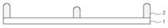
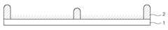
도 2는 도 1의 특정부분(A-A')에 대한 단면을 포함한 종래의 횡전계 방식 액정표시장치의 단면도이다.2 is a cross-sectional view of a conventional transverse electric field type liquid crystal display device including a cross section of a specific portion A-A 'of FIG. 1.
도 2를 참조하면, 종래의 횡전계 방식의 액정표시장치는 블랙매트릭스(8)와 서브 컬러필터(6)이 형성된 컬러필터 기판(5)과, 도 1에 도시된 서브픽셀(10)이 매트릭스 형태로 배열된 어레이 기판(22)으로 구성되고, 상기 컬러필터 기판(5)과 어레이 기판(22) 사이에는 앞서 설명한 액정(20)이 삽입되며, 상기 기판의 가장자리에 도포된 실런트(sealant)(미도시)에 의해 합착된다. 또한, 상기 컬러필터 기판(5)과 어레이 기판(22) 사이에 상기 액정(20)이 주입될 수 있는 공간을 마련하기 위해 스페이서(spacer)(미도시)가 산포된다.Referring to FIG. 2, a conventional transverse electric field type liquid crystal display device includes a matrix of a
도 1 및 도 2를 참조하면, 어레이 기판(22)에 형성된 서브픽셀(10)의 화상 표시영역 즉, 4블록(39)을 제외하고는 빛이 투과되지 않는 영역이 되는 것이며, 이에 따라 상기 4블록(39) 영역을 제외한 영역에 대해서는 상기 컬러필터 기판(5)의 블랙매트릭스(8)가 형성되어 있어 불필요한 빛을 차단하게 된다.
그러나, 상기 데이터 라인(15, 15')과 상기 데이터라인(15, 15')과 인접한 공통전극(54a, 54a')은 상기 블록(39) 영역에 해당하지 않아 도 2에 도시된 바와 같이 블랙매트릭스(8)에 의해 가려지게 되는데, 이와 같이 블랙매트릭스(8)로 상기 영역을 차단하는 경우에도 컬러필터 기판 및 어레이 기판(5, 22)의 미스얼라인(misalign)이 발생할 경우 빛샘 불량이 발생하게 된다.
특히 기판 크기가 커질 경우 상기 컬러필터 기판 및 어레이 기판(5, 22)의 미스얼라인 정도는 더욱 심해짐으로 도 2에 도시된 바와 같이 컬러필터 기판(5)의 블랙매트릭스(8) 폭이 상기 블록(39) 영역 일부를 덮도록 그 폭을 크게 가져가야 하며, 이 경우 최종적인 개구율의 감소를 가져온다.
또한, 도 2에 도시된 바와 같이 상기 블랙매트릭스(8)의 폭을 넓힌다 하더라도 이 부분에서의 빛의 굴절 효과에 의한 빛샘 현상이 발생할 수도 있는 것이다.
이와 같은 상기 빛샘 현상에 의해, 종래의 구조에 의한 횡전계 방식의 액정표시장치의 경우에는 액정표시장치의 표시 화면에 얼룩이 나타나는 현상이 발생된다.1 and 2, an image display area of the
However, the
In particular, when the substrate size increases, the misalignment degree of the color filter substrate and the
In addition, even if the width of the
Such a light leakage phenomenon causes a phenomenon in which a spot appears on the display screen of the liquid crystal display device in the case of a horizontal electric field type liquid crystal display device having a conventional structure.
삭제delete
삭제delete
본 발명은 데이터 라인 및 상기 데이터 라인 상에 또는 상기 데이터 라인과 인접한 공통전극 사이에 해당하는 어레이 기판 상의 영역에 패턴 스페이서를 형성하여, 상기 영역에 액정이 위치하지 않게 함으로써 빛샘 현상을 방지하는 횡전계 방식의 액정표시장치를 제공함에 그 목적이 있다.The present invention forms a pattern spacer in a region on an array substrate corresponding to a data line and the data line or between a common electrode adjacent to the data line, thereby preventing a liquid leakage in the region, thereby preventing a light leakage phenomenon. It is an object of the present invention to provide a liquid crystal display device.
상기 목적을 달성하기 위하여 본 발명에 의한 횡전계 방식의 액정표시장치는, 다수의 게이트 라인, 공통 라인, 데이터 라인에 의해 둘러싸여 정의되는 서브픽셀이 매트릭스 형태로 배열된 어레이 기판과, 블랙매트릭스와 서브 컬러필터가 형성된 컬러필터 기판과, 상기 데이터 라인 상에 형성되는 스페이서와, 상기 어레이 기판 및 컬러필터 기판 사이에 개재된 액정층이 포함되는 것을 특징으로 한다.In order to achieve the above object, a transverse electric field type liquid crystal display according to the present invention includes an array substrate in which subpixels defined by a plurality of gate lines, a common line, and a data line are arranged in a matrix form, a black matrix and a sub matrix. And a liquid crystal layer interposed between the color filter substrate on which the color filter is formed, the spacer formed on the data line, and the array substrate and the color filter substrate.
또한, 상기 어레이 기판 상에 형성된 다수의 게이트 라인 및 공통라인은 가로방향으로 서로 평행을 이루며 형성되어 있고, 상기 다수의 데이터 라인은 세로방향으로 상기 게이트 라인 및 공통 라인과 교차하여 형성됨을 특징으로 한다.In addition, the plurality of gate lines and the common line formed on the array substrate are formed parallel to each other in the horizontal direction, and the plurality of data lines are formed to cross the gate line and the common line in the longitudinal direction. .
또한, 상기 서브 픽셀은 박막트랜지스터와, 상기 공통 라인에서 분기된 다수의 공통전극과, 상기 박막트랜지스터의 드레인 전극과 연결된 인출배선에서 분기된 다수의 화소전극으로 구성되며, 상기 다수의 공통전극과 상기 화소전극은 서로 엇갈리게 구성되어 있음을 특징으로 한다.The subpixel may include a thin film transistor, a plurality of common electrodes branched from the common line, and a plurality of pixel electrodes branched from a drawing wiring connected to the drain electrode of the thin film transistor. The pixel electrodes are characterized in that they are alternate with each other.
또한, 상기 스페이서는 상기 포토레지스트막으로 이루어지며, 상기 데이터 라인 및 상기 데이터 라인과 인접한 공통전극 사이를 포함하는 어레이 기판 상의 영역에 패터닝되어 형성됨을 특징으로 한다.In addition, the spacer is formed of the photoresist layer and is patterned and formed in an area on the array substrate including the data line and the common electrode adjacent to the data line.
또한, 상기 블랙매트릭스는 어레이 기판 상의 상기 데이터 라인 및 상기 데이터 라인과 인접한 공통전극 사이를 포함한 영역을 통과한 빛이 차단되는 컬러필터 기판 상의 영역에 형성됨을 특징으로 한다.The black matrix may be formed in an area on a color filter substrate in which light passing through an area including an area between the data line and the common line adjacent to the data line is blocked.
또한, 상기 스페이서는 상기 데이터 라인 및 상기 데이터 라인과 인접한 공통전극 사이에 해당하는 어레이 기판 상의 영역에 형성되며, 상기 데이터 라인의 상부 영역에는 액정이 위치하고, 상기 액정을 중심으로 스페이서가 분리되어 형성됨을 특징으로 한다.In addition, the spacer is formed in a region on the array substrate corresponding to the data line and the common electrode adjacent to the data line, the liquid crystal is located in the upper region of the data line, the spacer is formed by separating the spacer around the liquid crystal. It features.
이와 같은 본 발명에 의하면, 빛샘 현상을 방지하여 표시화면에 얼룩이 발생되는 것을 최소화하며, 또한, 컬러필터 기판에 형성되는 블랙매트릭스의 폭을 줄여 결과적으로 개구율을 향상시키게 한다.According to the present invention, the light leakage phenomenon is prevented to minimize the occurrence of unevenness on the display screen, and also the width of the black matrix formed on the color filter substrate is reduced to improve the aperture ratio.
본 발명에 의한 횡전계방식의 액정표시장치에 대한 설명에 앞서 액정표시장치에 있어서 컬러필터 기판과 어레이 기판 간의 일정한 공간을 형성하기 위해 삽입되는 스페이서(spacer)에 대해 설명하도록 한다.Prior to the description of the transverse electric field type liquid crystal display device according to the present invention, a spacer inserted to form a predetermined space between the color filter substrate and the array substrate in the liquid crystal display device will be described.
상기 스페이서는 셀 갭을 균일하게 유지하기 위해 산포하는 것으로 섬유 모양의 스페이서, 탄성볼 스페이서 및 고착성 스페이서 등의 종류가 있다. 그러나, 이러한 스페이서 입자는 기판 상에 무 작위로 산포되기 때문에 유효 화소부 내에 상기 스페이서가 존재하면 스페이서가 비치거나, 입사광이 산란되어 액정 패널의 콘트라스트가 저하되는 문제가 있었다.The spacers are dispersed in order to maintain the cell gap uniformly, and there are kinds of spacers such as fibrous spacers, elastic ball spacers, and adhesive spacers. However, since the spacer particles are randomly scattered on the substrate, when the spacer is present in the effective pixel portion, there is a problem that the spacer is reflected or the incident light is scattered and the contrast of the liquid crystal panel is lowered.
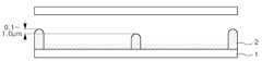
상기 문제를 해결하기 위해 스페이서를 포토리소그래피(photolithography) 공정을 이용한 방법으로 형성하는 것이 제안되었다. 이 방법은 포토레지스트막을 기판에 도포하고, 소정의 마스크(mask)를 통하여 자외선을 조사한 다음 현상하여 도트(dot)나 스트라이프(stripe) 형태의 스페이서를 형성시킬 수 있기 때문에 유효 화소부 이외의 부분에 스페이서를 형성시킬 수 있게 되며, 상기 셀 갭을 포토레지스트막의 두께로 조절할 수 있기 때문에 갭 폭의 조절이 용이하고, 정밀도가 높은 장점이 있다. 이와 같은 액정표시장치의 스페이서 형성 방법을 첨부한 도 3a 내지 도 3d의 공정 단면도를 참조하여 설명하면 다음과 같다.In order to solve the above problem, it has been proposed to form a spacer by a method using a photolithography process. In this method, a photoresist film is applied to a substrate, ultraviolet rays are irradiated through a predetermined mask, and then developed to form a dot or stripe-shaped spacer. Since the spacers can be formed and the cell gap can be adjusted by the thickness of the photoresist film, the gap width can be easily adjusted and the precision is high. Referring to the process cross-sectional view of FIGS. 3A to 3D attached to the spacer forming method of the liquid crystal display device as follows.
도 3a 내지 도 3d는 액정표시장치의 스페이서 형성 방법을 도시한 공정 단면도이다.3A to 3D are cross-sectional views illustrating a method of forming a spacer of a liquid crystal display device.
먼저, 도 3a에 도시한 바와 같이 하부 기판(1) 즉, 어레이 기판 상에 포토레지스트막(2)을 스핀-코팅(spin-coating) 방법 등으로 도포한다. 이 때의 상기 하부기판은 서브픽셀이 매트릭스 형태로 배열된 상태의 하부기판을 의미하는 것이다.First, as shown in FIG. 3A, the
그리고, 도 3b에 도시한 바와 같이 상기 포토레지스트막(2)에 마스크(미도시)를 사용하여 자외선을 선택적으로 조사한 다음 현상하여 포토레지스트막(2)의 패턴을 형성한다.As shown in FIG. 3B, ultraviolet rays are selectively irradiated onto the
다음으로 도 3c에 도시한 바와 같이 상기 포토레지스트막(2)의 패턴이 형성된 하부 기판(1) 상에 러빙(rubbing)을 수행하여 후속 액정이 채워질 때, 원하는 배향을 갖도록 한다.
마지막으로 도 3d에 도시한 바와 같이 상기 러빙이 수행된 상기 어레이 기판 즉 하부 기판(1) 상에 컬러필터 기판(3)을 합착시킨다.
이하 첨부된 도면을 참조하여 본 발명에 의한 실시예를 상세히 설명하도록 한다.
도 4는 본 발명의 일 실시예에 의한 횡전계 방식의 액정표시장치의 단면도이다.
단, 도 4는 어레이 기판의 특정 서브픽셀 영역을 포함한 단면도이며, 본 발명에 의한 어레이 기판은 도 1에 도시된 종래의 어레이 기판과 그 구성이 동일하다. 따라서, 도 1과 동일한 구성요소의 경우에는 동일한 도면부호를 사용한다.Next, as shown in FIG. 3C, rubbing is performed on the
Finally, as shown in FIG. 3D, the color filter substrate 3 is bonded onto the array substrate, ie, the
Hereinafter, exemplary embodiments of the present invention will be described in detail with reference to the accompanying drawings.
4 is a cross-sectional view of a transverse electric field type liquid crystal display device according to an exemplary embodiment of the present invention.
4 is a cross-sectional view including a specific subpixel region of the array substrate, and the array substrate according to the present invention has the same configuration as the conventional array substrate shown in FIG. Therefore, the same reference numerals are used for the same components as in FIG. 1.
삭제delete
삭제delete
삭제delete
도 4를 참조하면, 본 발명의 일 실시예에 의한 횡전계 방식의 액정표시장치는 블랙매트릭스(8)와 서브 컬러필터(6)가 형성된 컬러필터 기판(5)과, 도 1에 도시된 서브픽셀(10)이 매트릭스 형태로 배열된 어레이 기판(22)으로 구성되고, 상기 컬러필터 기판(5)과 어레이 기판(22) 사이에는 앞서 설명한 액정(20)이 삽입되며, 상기 기판(5, 22)의 가장자리에 도포된 실런트(sealant)(미도시)에 의해 합착된다. 또한, 상기 컬러필터 기판(5)과 어레이 기판(22) 사이에 상기 액정(20)이 주입될 수 있는 공간을 마련하기 위해 스페이서(spacer)(40)가 형성된다.Referring to FIG. 4, a transverse electric field type liquid crystal display according to an exemplary embodiment of the present invention includes a
단, 상기 스페이서는 패턴 스페이서(pattern spacer)(40)로서 도 3에 도시된 형성 방법에 의해 형성되며, 그 형성 영역이 데이터 라인(15, 15') 및 상기 데이터 라인(15, 15')에 인접한 공통전극(54a, 54a') 사이를 포함하는 어레이 기판(22) 상의 영역임을 그 특징으로 한다.However, the spacer is formed as a
도 4를 참조하면, 어레이 기판(22)에 형성된 서브픽셀의 화상 표시영역 즉, 4블록(39) 영역을 제외하고는 빛이 투과되지 않는 영역이 되는 것이며, 이에 따라 상기 4블록(39) 영역을 제외한 영역에 대해서는 상기 컬러필터 기판(5)의 블랙매트릭스(8)가 형성되어 있어 불필요한 빛을 차단하게 된다.Referring to FIG. 4, the light is not transmitted except the image display area of the subpixel formed on the
이 때, 종래의 경우에는 도 2에 도시된 바와 같이 데이터 라인(15, 15')과 상기 데이터 라인(15, 15')과 인접한 공통전극(54a, 54a')은 상기 블록(39) 영역에 해당하지 않아 블랙매트릭스(8)에 의해 가려지게 되는데, 이와 같이 블랙매트릭스(8)로 상기 영역을 차단하는 경우에도 상기 컬러필터 기판(5)과 어레이 기판(22) 사이에 형성된 액정(20)에 의해 하부 백 라이트의 빛이 굴절되어 상기 블랙매트릭스(8)가 형성되지 않은 영역으로 투과되어 불량을 일으키게 된다. 또한, 이 경우 상기 블랙매트릭스(8)은 그 폭이 상기 블록(39) 영역 일부를 덮도록 넓게 형성되어 개구율이 감소된다.In this case, as shown in FIG. 2, the data lines 15 and 15 ′ and the
이를 극복하기 위해 본 발명의 일 실시예는 도 4에 도시된 바와 같이 상기 데이터 라인(15, 15') 및 상기 데이터 라인(15, 15')에 인접한 공통전극(54a, 54a') 사이를 포함하는 어레이 기판(22) 상의 영역에 상기 패턴 스페이서(40)를 형성한다.In order to overcome this, an embodiment of the present invention includes a gap between the data lines 15 and 15 'and the
이와 같이 패턴 스페이서(40)를 상기 데이터 라인(15, 15') 및 상기 데이터 라인(15, 15')과 인접한 공통전극(54a, 54a') 사이를 포함하는 어레이 기판(22) 상의 영역에 형성하면, 상기 영역에 대해서는 액정(20)이 위치할 수 없게 되므로 결국 상기 영역을 투과하는 하부 백 라이트의 빛이 normally black mode 일 경우 자동적으로 투과되지 않는다. 따라서, 컬러필터 기판(5) 및 어레이 기판(22)이 미스얼라인 되더라도 빛샘 현상을 근원적으로 차단할 수 있다.
결국 이에 의해 종래의 경우와 같이 상기 빛샘 현상을 최소화하기 위해 블랙매트릭스(8)의 폭을 늘릴 필요가 없게 되어 화면 표시 영역의 개구율이 향상되는 것이다.
이에 더하여, 상기 패턴 스페이서(40)의 에지는 상기 데이터 라인(15, 15')과 마주하는 상기 공통전극(54a, 54a')의 제 1 식각면과 대향하는 제 2 식각면과 일치할 수 있다. 또한, 상기 블랙매트릭스(8)의 식각면은 상기 제 2 식각면과 일치할 수 있다. 이에 따라, 상기 패턴 스페이서(40)의 에지는 상기 블랙매트릭스(8)의 식각면과 일치할 수 있다.
도 5는 본 발명의 다른 실시예에 의한 횡전계 방식의 액정표시장치의 단면도이다.
단, 도 5는 어레이 기판의 특정 서브픽셀 영역을 포함한 단면도이며, 본 발명에 의한 어레이 기판은 도 1에 도시된 종래의 어레이 기판과 그 구성이 동일하다. 따라서, 도 1과 동일한 구성요소의 경우에는 동일한 도면부호를 사용한다.
도 5를 참조하면, 도 4와 전체적인 구성이 유사하며, 다만, 상기 어레이 기판(22)과 컬러필터 기판(5) 사이에 개재되는 패턴 스페이서(50)의 형성 위치가 다른 점에서 그 특징이 있다.
도 5에 도시된 본 발명의 다른 실시예는 어레이 기판(22) 상에 배열된 데이터 라인(15, 15')의 폭이 넓은 경우에 적용되는 것으로 상기 패턴 스페이서(50)가 데이터 라인(15, 15') 및 상기 데이터 라인(15, 15')과 인접한 공통전극(54a, 54a') 사이에 해당하는 어레이 기판(22) 상의 영역에 형성된다.
즉, 상기 패턴 스페이서(50)는 상기 각 데이터 라인(15, 15')의 양측에 배치된다. 또한, 상기 패턴 스페이서(50)의 에지는 상기 데이터 라인(15, 15')과 마주하는 상기 공통전극(54a, 54a')의 제 1 식각면과 대향하는 제 2 식각면과 일치할 수 있다. 또한, 상기 블랙매트릭스(8)의 식각면은 상기 패턴 스페이서(50)의 에지와 일치할 수 있다. 따라서, 상기 블랙매트릭스(8)의 식각면은 상기 공통전극(54a, 54a')의 제 2 식각면과 일치할 수 있다.
즉, 상기 데이터 라인(15, 15')의 상부 영역에는 상기 패턴 스페이서(50)가 형성되어 있지 않아 그 영역에는 액정(20)이 위치할 수 있는 것이다.
결국, 상기 데이터 라인(15, 15')의 상부 영역에는 액정(20)이 위치하며, 상기 액정(20)을 중심으로 스페이서(50)가 분리되어 형성되어 있는 것이다. 그러나, 이 경우에도 상기 데이터 라인(15, 15')의 상부에 위치한 액정(20)에 빛이 비춰지더라도 블랙매트릭스(8)에 의해 모두 차단되므로 빛샘 현상이 발생되지 못한다.
결국 도 5에 도시된 바와 같이 패턴 스페이서(50)를 상기 데이터 라인(15, 15') 및 상기 데이터 라인(15, 15')과 인접한 공통전극(54a, 54a') 사이에 해당하는 어레이 기판(22) 상의 영역에 형성하면, 상기 영역에 대해서는 액정(20)이 위치할 수 없게 되므로 액정(20)에 의한 빛의 굴절이 발생되지 않으므로 빛샘 현상이 발생되지 않게 된다.
또한, 이 경우에도 종래의 경우와 같이 상기 빛샘 현상을 최소화하기 위해 블랙매트릭스(8)의 폭을 늘릴 필요가 없으므로 화면 표시 영역의 개구율이 향상되는 효과가 있는 것이다.As such, the
As a result, it is not necessary to increase the width of the
In addition, an edge of the
5 is a cross-sectional view of a transverse electric field type liquid crystal display device according to another exemplary embodiment of the present invention.
5 is a cross-sectional view including a specific subpixel region of the array substrate, and the array substrate according to the present invention has the same configuration as the conventional array substrate shown in FIG. Therefore, the same reference numerals are used for the same components as in FIG. 1.
Referring to FIG. 5, the overall configuration is similar to that of FIG. 4, except that the formation positions of the pattern spacers 50 interposed between the
Another embodiment of the present invention shown in FIG. 5 is applicable to the case where the widths of the data lines 15 and 15 'arranged on the
That is, the
That is, since the
As a result, the
As a result, as shown in FIG. 5, the patterned
Also in this case, since the width of the
삭제delete
삭제delete
삭제delete
삭제delete
삭제delete
삭제delete
삭제delete
이상의 설명에서와 같이 본 발명에 따른 횡전계 방식의 액정표시장치에 의하면, 빛샘 현상을 방지하여 표시화면에 얼룩이 발생되는 것을 최소화하며, 또한, 컬러필터 기판에 형성되는 블랙매트릭스의 폭을 줄여 결과적으로 개구율을 향상시키는 장점이 있다.According to the liquid crystal display device of the transverse electric field method according to the present invention as described above, to prevent light leakage phenomenon to minimize the occurrence of stains on the display screen, and also to reduce the width of the black matrix formed on the color filter substrate as a result There is an advantage of improving the aperture ratio.
Claims (17)
Translated fromKoreanPriority Applications (2)
| Application Number | Priority Date | Filing Date | Title |
|---|---|---|---|
| KR1020020086636AKR100789086B1 (en) | 2002-12-30 | 2002-12-30 | In-Plane Switching mode Liquid Crystal Display Device |
| US10/465,840US6930747B2 (en) | 2002-12-30 | 2003-06-20 | In-plane switching mode liquid crystal display device |
Applications Claiming Priority (1)
| Application Number | Priority Date | Filing Date | Title |
|---|---|---|---|
| KR1020020086636AKR100789086B1 (en) | 2002-12-30 | 2002-12-30 | In-Plane Switching mode Liquid Crystal Display Device |
Publications (2)
| Publication Number | Publication Date |
|---|---|
| KR20040060107A KR20040060107A (en) | 2004-07-06 |
| KR100789086B1true KR100789086B1 (en) | 2007-12-26 |
Family
ID=32653224
Family Applications (1)
| Application Number | Title | Priority Date | Filing Date |
|---|---|---|---|
| KR1020020086636AExpired - LifetimeKR100789086B1 (en) | 2002-12-30 | 2002-12-30 | In-Plane Switching mode Liquid Crystal Display Device |
Country Status (2)
| Country | Link |
|---|---|
| US (1) | US6930747B2 (en) |
| KR (1) | KR100789086B1 (en) |
Cited By (1)
| Publication number | Priority date | Publication date | Assignee | Title |
|---|---|---|---|---|
| US8810745B2 (en) | 2011-09-29 | 2014-08-19 | Samsung Display Co., Ltd. | Liquid crystal display |
Families Citing this family (11)
| Publication number | Priority date | Publication date | Assignee | Title |
|---|---|---|---|---|
| TW591287B (en)* | 2003-04-10 | 2004-06-11 | Au Optronics Corp | Liquid crystal display with an uniform common voltage and method thereof |
| KR20060024939A (en)* | 2004-09-15 | 2006-03-20 | 엘지.필립스 엘시디 주식회사 | Color filter substrate for liquid crystal display device and manufacturing method thereof |
| JP2006098623A (en)* | 2004-09-29 | 2006-04-13 | Hitachi Displays Ltd | Liquid crystal display |
| KR100672648B1 (en)* | 2004-12-14 | 2007-01-24 | 엘지.필립스 엘시디 주식회사 | Liquid crystal display and manufacturing method thereof |
| TW200643531A (en)* | 2005-06-03 | 2006-12-16 | Innolux Display Corp | Liquid crystal display device |
| CN100426101C (en)* | 2005-06-25 | 2008-10-15 | 群康科技(深圳)有限公司 | Liquid crystal display device |
| JP4876470B2 (en)* | 2005-07-29 | 2012-02-15 | 三菱電機株式会社 | Display element |
| WO2012094402A1 (en) | 2011-01-04 | 2012-07-12 | Espinosa Thomas M | Building with roof trusses directly connected to the foundation |
| US11656552B2 (en)* | 2015-07-16 | 2023-05-23 | Ming-An Hsu | Device having color resists pattern and method for manufacturing the same |
| CN207164424U (en)* | 2017-09-30 | 2018-03-30 | 合肥鑫晟光电科技有限公司 | Array base palte, display panel and display device |
| US11700977B2 (en) | 2019-12-30 | 2023-07-18 | Pardha S. Gadde | Automatic system for providing full body shower to a user |
Citations (4)
| Publication number | Priority date | Publication date | Assignee | Title |
|---|---|---|---|---|
| JP2000019526A (en)* | 1998-06-30 | 2000-01-21 | Hitachi Ltd | Liquid crystal display |
| JP2000019527A (en) | 1998-06-30 | 2000-01-21 | Hitachi Ltd | Liquid crystal display |
| JP2000275654A (en) | 1999-03-24 | 2000-10-06 | Hitachi Ltd | Liquid crystal display device and manufacturing method thereof |
| KR20000062978A (en)* | 1999-03-26 | 2000-10-25 | 가네꼬 히사시 | Liquid crystal display device of latitudinal electric field type having protruded spacer |
Family Cites Families (7)
| Publication number | Priority date | Publication date | Assignee | Title |
|---|---|---|---|---|
| KR100225910B1 (en)* | 1996-04-04 | 1999-10-15 | 구자홍 | LIQUID CRYSTAL DISPLAY DEVICE |
| US6337730B1 (en)* | 1998-06-02 | 2002-01-08 | Denso Corporation | Non-uniformly-rigid barrier wall spacers used to correct problems caused by thermal contraction of smectic liquid crystal material |
| JP2001021902A (en)* | 1999-07-09 | 2001-01-26 | Toshiba Corp | Liquid crystal display |
| KR100545020B1 (en) | 1999-12-31 | 2006-01-24 | 엘지.필립스 엘시디 주식회사 | Liquid crystal panel in planar switching mode and its manufacturing method |
| TWI225558B (en)* | 2000-04-24 | 2004-12-21 | Nec Lcd Technologies Ltd | Liquid crystal display and fabrication method thereof |
| JP4609679B2 (en)* | 2000-07-19 | 2011-01-12 | 日本電気株式会社 | Liquid crystal display |
| US7179512B2 (en)* | 2002-05-14 | 2007-02-20 | Fujitsu Limited | Liquid crystal display and manufacturing method of same |
- 2002
- 2002-12-30KRKR1020020086636Apatent/KR100789086B1/ennot_activeExpired - Lifetime
- 2003
- 2003-06-20USUS10/465,840patent/US6930747B2/ennot_activeExpired - Lifetime
Patent Citations (4)
| Publication number | Priority date | Publication date | Assignee | Title |
|---|---|---|---|---|
| JP2000019526A (en)* | 1998-06-30 | 2000-01-21 | Hitachi Ltd | Liquid crystal display |
| JP2000019527A (en) | 1998-06-30 | 2000-01-21 | Hitachi Ltd | Liquid crystal display |
| JP2000275654A (en) | 1999-03-24 | 2000-10-06 | Hitachi Ltd | Liquid crystal display device and manufacturing method thereof |
| KR20000062978A (en)* | 1999-03-26 | 2000-10-25 | 가네꼬 히사시 | Liquid crystal display device of latitudinal electric field type having protruded spacer |
Cited By (1)
| Publication number | Priority date | Publication date | Assignee | Title |
|---|---|---|---|---|
| US8810745B2 (en) | 2011-09-29 | 2014-08-19 | Samsung Display Co., Ltd. | Liquid crystal display |
Also Published As
| Publication number | Publication date |
|---|---|
| US6930747B2 (en) | 2005-08-16 |
| KR20040060107A (en) | 2004-07-06 |
| US20040125301A1 (en) | 2004-07-01 |
Similar Documents
| Publication | Publication Date | Title |
|---|---|---|
| KR100403648B1 (en) | Liquid crystal display device and method of fabricating the same | |
| KR20090083060A (en) | Liquid crystal display | |
| JP4202062B2 (en) | Liquid crystal display | |
| US8451411B2 (en) | Display panel having a domain divider | |
| KR20100007081A (en) | Display substrate and display panel having the same | |
| KR100789086B1 (en) | In-Plane Switching mode Liquid Crystal Display Device | |
| KR100959367B1 (en) | Transverse electric field type liquid crystal display device | |
| KR20130104224A (en) | Liquid crystal display device | |
| KR100831278B1 (en) | Multi Domain Liquid Crystal Display | |
| KR101540302B1 (en) | Display substrate and liquid crystal display panel having the same | |
| KR100603829B1 (en) | Fringe field switching mode LCD | |
| KR100582598B1 (en) | LCD to prevent light leakage | |
| KR100903650B1 (en) | Liquid crystal display | |
| KR20040061786A (en) | Method for fabricating for an array substrate for In-Plane switching mode LCD | |
| US20050190337A1 (en) | Liquid crystal display device and method for manufacturing the same | |
| KR100630878B1 (en) | Fringe Field Switching Mode Liquid Crystal Display Device and Method for Manufacturing the same | |
| KR101048701B1 (en) | Manufacturing method of color filter substrate | |
| KR20090036870A (en) | LCD Display | |
| KR101174145B1 (en) | liquid crystal display device | |
| KR100867167B1 (en) | LCD and its manufacturing method | |
| KR102081136B1 (en) | Liquid crystal display device | |
| KR20060057956A (en) | Liquid crystal display device comprising a counter electrode having a hole and a manufacturing method thereof | |
| KR20030033833A (en) | Multi-domain Liquid Crystal Display Device And Method For Fabricating The Same | |
| KR101192630B1 (en) | Array substrate for In-Plane switching mode LCD | |
| KR100936951B1 (en) | LCD Display |
Legal Events
| Date | Code | Title | Description |
|---|---|---|---|
| PA0109 | Patent application | Patent event code:PA01091R01D Comment text:Patent Application Patent event date:20021230 | |
| PG1501 | Laying open of application | ||
| A201 | Request for examination | ||
| PA0201 | Request for examination | Patent event code:PA02012R01D Patent event date:20060726 Comment text:Request for Examination of Application Patent event code:PA02011R01I Patent event date:20021230 Comment text:Patent Application | |
| E902 | Notification of reason for refusal | ||
| PE0902 | Notice of grounds for rejection | Comment text:Notification of reason for refusal Patent event date:20070917 Patent event code:PE09021S01D | |
| E701 | Decision to grant or registration of patent right | ||
| PE0701 | Decision of registration | Patent event code:PE07011S01D Comment text:Decision to Grant Registration Patent event date:20071130 | |
| GRNT | Written decision to grant | ||
| PR0701 | Registration of establishment | Comment text:Registration of Establishment Patent event date:20071218 Patent event code:PR07011E01D | |
| PR1002 | Payment of registration fee | Payment date:20071218 End annual number:3 Start annual number:1 | |
| PG1601 | Publication of registration | ||
| G170 | Re-publication after modification of scope of protection [patent] | ||
| PG1701 | Publication of correction | ||
| PR1001 | Payment of annual fee | Payment date:20100929 Start annual number:4 End annual number:4 | |
| PR1001 | Payment of annual fee | Payment date:20110915 Start annual number:5 End annual number:5 | |
| FPAY | Annual fee payment | Payment date:20120928 Year of fee payment:6 | |
| PR1001 | Payment of annual fee | Payment date:20120928 Start annual number:6 End annual number:6 | |
| FPAY | Annual fee payment | Payment date:20130930 Year of fee payment:7 | |
| PR1001 | Payment of annual fee | Payment date:20130930 Start annual number:7 End annual number:7 | |
| FPAY | Annual fee payment | Payment date:20141124 Year of fee payment:8 | |
| PR1001 | Payment of annual fee | Payment date:20141124 Start annual number:8 End annual number:8 | |
| FPAY | Annual fee payment | Payment date:20161118 Year of fee payment:10 | |
| PR1001 | Payment of annual fee | Payment date:20161118 Start annual number:10 End annual number:10 | |
| FPAY | Annual fee payment | Payment date:20171116 Year of fee payment:11 | |
| PR1001 | Payment of annual fee | Payment date:20171116 Start annual number:11 End annual number:11 | |
| FPAY | Annual fee payment | Payment date:20181114 Year of fee payment:12 | |
| PR1001 | Payment of annual fee | Payment date:20181114 Start annual number:12 End annual number:12 | |
| FPAY | Annual fee payment | Payment date:20191113 Year of fee payment:13 | |
| PR1001 | Payment of annual fee | Payment date:20191113 Start annual number:13 End annual number:13 | |
| PR1001 | Payment of annual fee | Payment date:20201119 Start annual number:14 End annual number:14 | |
| PR1001 | Payment of annual fee | Payment date:20211116 Start annual number:15 End annual number:15 | |
| PR1001 | Payment of annual fee | Payment date:20221115 Start annual number:16 End annual number:16 | |
| PC1801 | Expiration of term | Termination date:20230629 Termination category:Expiration of duration |