KR100788361B1 - Formation method of MOSFET device - Google Patents
Formation method of MOSFET deviceDownload PDFInfo
- Publication number
- KR100788361B1 KR100788361B1KR1020060126088AKR20060126088AKR100788361B1KR 100788361 B1KR100788361 B1KR 100788361B1KR 1020060126088 AKR1020060126088 AKR 1020060126088AKR 20060126088 AKR20060126088 AKR 20060126088AKR 100788361 B1KR100788361 B1KR 100788361B1
- Authority
- KR
- South Korea
- Prior art keywords
- insulating film
- gate insulating
- forming
- present
- dielectric constant
- Prior art date
- Legal status (The legal status is an assumption and is not a legal conclusion. Google has not performed a legal analysis and makes no representation as to the accuracy of the status listed.)
- Expired - Fee Related
Links
Images


Classifications
- H—ELECTRICITY
- H01—ELECTRIC ELEMENTS
- H01L—SEMICONDUCTOR DEVICES NOT COVERED BY CLASS H10
- H01L21/00—Processes or apparatus adapted for the manufacture or treatment of semiconductor or solid state devices or of parts thereof
- H01L21/02—Manufacture or treatment of semiconductor devices or of parts thereof
- H01L21/04—Manufacture or treatment of semiconductor devices or of parts thereof the devices having potential barriers, e.g. a PN junction, depletion layer or carrier concentration layer
- H01L21/18—Manufacture or treatment of semiconductor devices or of parts thereof the devices having potential barriers, e.g. a PN junction, depletion layer or carrier concentration layer the devices having semiconductor bodies comprising elements of Group IV of the Periodic Table or AIIIBV compounds with or without impurities, e.g. doping materials
- H01L21/28—Manufacture of electrodes on semiconductor bodies using processes or apparatus not provided for in groups H01L21/20 - H01L21/268
- H01L21/28008—Making conductor-insulator-semiconductor electrodes
- H01L21/28017—Making conductor-insulator-semiconductor electrodes the insulator being formed after the semiconductor body, the semiconductor being silicon
- H01L21/28158—Making the insulator
- H01L21/28167—Making the insulator on single crystalline silicon, e.g. using a liquid, i.e. chemical oxidation
- H01L21/28202—Making the insulator on single crystalline silicon, e.g. using a liquid, i.e. chemical oxidation in a nitrogen-containing ambient, e.g. nitride deposition, growth, oxynitridation, NH3 nitridation, N2O oxidation, thermal nitridation, RTN, plasma nitridation, RPN
- H—ELECTRICITY
- H01—ELECTRIC ELEMENTS
- H01L—SEMICONDUCTOR DEVICES NOT COVERED BY CLASS H10
- H01L21/00—Processes or apparatus adapted for the manufacture or treatment of semiconductor or solid state devices or of parts thereof
- H01L21/02—Manufacture or treatment of semiconductor devices or of parts thereof
- H01L21/04—Manufacture or treatment of semiconductor devices or of parts thereof the devices having potential barriers, e.g. a PN junction, depletion layer or carrier concentration layer
- H01L21/18—Manufacture or treatment of semiconductor devices or of parts thereof the devices having potential barriers, e.g. a PN junction, depletion layer or carrier concentration layer the devices having semiconductor bodies comprising elements of Group IV of the Periodic Table or AIIIBV compounds with or without impurities, e.g. doping materials
- H01L21/28—Manufacture of electrodes on semiconductor bodies using processes or apparatus not provided for in groups H01L21/20 - H01L21/268
- H01L21/28008—Making conductor-insulator-semiconductor electrodes
- H01L21/28017—Making conductor-insulator-semiconductor electrodes the insulator being formed after the semiconductor body, the semiconductor being silicon
- H01L21/28158—Making the insulator
- H01L21/28167—Making the insulator on single crystalline silicon, e.g. using a liquid, i.e. chemical oxidation
- H01L21/28185—Making the insulator on single crystalline silicon, e.g. using a liquid, i.e. chemical oxidation with a treatment, e.g. annealing, after the formation of the gate insulator and before the formation of the definitive gate conductor
- H—ELECTRICITY
- H01—ELECTRIC ELEMENTS
- H01L—SEMICONDUCTOR DEVICES NOT COVERED BY CLASS H10
- H01L21/00—Processes or apparatus adapted for the manufacture or treatment of semiconductor or solid state devices or of parts thereof
- H01L21/02—Manufacture or treatment of semiconductor devices or of parts thereof
- H01L21/04—Manufacture or treatment of semiconductor devices or of parts thereof the devices having potential barriers, e.g. a PN junction, depletion layer or carrier concentration layer
- H01L21/18—Manufacture or treatment of semiconductor devices or of parts thereof the devices having potential barriers, e.g. a PN junction, depletion layer or carrier concentration layer the devices having semiconductor bodies comprising elements of Group IV of the Periodic Table or AIIIBV compounds with or without impurities, e.g. doping materials
- H01L21/28—Manufacture of electrodes on semiconductor bodies using processes or apparatus not provided for in groups H01L21/20 - H01L21/268
- H01L21/28008—Making conductor-insulator-semiconductor electrodes
- H01L21/28017—Making conductor-insulator-semiconductor electrodes the insulator being formed after the semiconductor body, the semiconductor being silicon
- H01L21/28158—Making the insulator
- H01L21/28167—Making the insulator on single crystalline silicon, e.g. using a liquid, i.e. chemical oxidation
- H01L21/28194—Making the insulator on single crystalline silicon, e.g. using a liquid, i.e. chemical oxidation by deposition, e.g. evaporation, ALD, CVD, sputtering, laser deposition
- H—ELECTRICITY
- H10—SEMICONDUCTOR DEVICES; ELECTRIC SOLID-STATE DEVICES NOT OTHERWISE PROVIDED FOR
- H10D—INORGANIC ELECTRIC SEMICONDUCTOR DEVICES
- H10D64/00—Electrodes of devices having potential barriers
- H10D64/60—Electrodes characterised by their materials
- H10D64/66—Electrodes having a conductor capacitively coupled to a semiconductor by an insulator, e.g. MIS electrodes
- H10D64/68—Electrodes having a conductor capacitively coupled to a semiconductor by an insulator, e.g. MIS electrodes characterised by the insulator, e.g. by the gate insulator
- H10D64/681—Electrodes having a conductor capacitively coupled to a semiconductor by an insulator, e.g. MIS electrodes characterised by the insulator, e.g. by the gate insulator having a compositional variation, e.g. multilayered
- H10D64/685—Electrodes having a conductor capacitively coupled to a semiconductor by an insulator, e.g. MIS electrodes characterised by the insulator, e.g. by the gate insulator having a compositional variation, e.g. multilayered being perpendicular to the channel plane
- H—ELECTRICITY
- H10—SEMICONDUCTOR DEVICES; ELECTRIC SOLID-STATE DEVICES NOT OTHERWISE PROVIDED FOR
- H10D—INORGANIC ELECTRIC SEMICONDUCTOR DEVICES
- H10D64/00—Electrodes of devices having potential barriers
- H10D64/60—Electrodes characterised by their materials
- H10D64/66—Electrodes having a conductor capacitively coupled to a semiconductor by an insulator, e.g. MIS electrodes
- H10D64/68—Electrodes having a conductor capacitively coupled to a semiconductor by an insulator, e.g. MIS electrodes characterised by the insulator, e.g. by the gate insulator
- H10D64/691—Electrodes having a conductor capacitively coupled to a semiconductor by an insulator, e.g. MIS electrodes characterised by the insulator, e.g. by the gate insulator comprising metallic compounds, e.g. metal oxides or metal silicates
Landscapes
- Engineering & Computer Science (AREA)
- Microelectronics & Electronic Packaging (AREA)
- Condensed Matter Physics & Semiconductors (AREA)
- General Physics & Mathematics (AREA)
- Manufacturing & Machinery (AREA)
- Computer Hardware Design (AREA)
- Physics & Mathematics (AREA)
- Power Engineering (AREA)
- Chemical & Material Sciences (AREA)
- Chemical Kinetics & Catalysis (AREA)
- Crystallography & Structural Chemistry (AREA)
- General Chemical & Material Sciences (AREA)
- Insulated Gate Type Field-Effect Transistor (AREA)
- Formation Of Insulating Films (AREA)
Abstract
Translated fromKoreanDescription
Translated fromKorean도 1a 내지 도 1c는 본 발명의 실시예에 따른 모스펫 소자의 형성 방법을 설명하기 위한 순차적인 공정 단면도.1A to 1C are sequential process cross-sectional views for explaining a method of forming a MOSFET device according to an embodiment of the present invention.
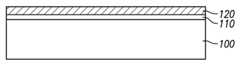
도 2는 본 발명에 따라 형성된 모스펫 소자의 게이트 절연막을 도시한 단면도.2 is a cross-sectional view showing a gate insulating film of the MOSFET device formed in accordance with the present invention.
< 도면의 주요 부분에 대한 부호의 설명 ><Description of Symbols for Main Parts of Drawings>
100 : 실리콘 반도체 기판100: silicon semiconductor substrate
110 : 제 1 게이트 절연막110: first gate insulating film
120 : 제 2 게이트 절연막120: second gate insulating film
본 발명은 모스펫 소자의 형성 방법에 관한 것으로, 특히 고 유전 상수(high-k)를 갖는 절연막으로 이루어진 게이트 절연막에 대해 어닐링(annealing) 공정을 수행함으로써 게이트 절연막의 신뢰성 및 소자의 동작 특성을 크게 향상시킬 수 있는 모스펫 소자의 형성 방법에 관한 것이다.BACKGROUND OF THE INVENTION 1. Field of the Invention The present invention relates to a method for forming a MOSFET device, and in particular, by performing an annealing process on a gate insulating film made of an insulating film having a high dielectric constant (high-k), greatly improving the reliability of the gate insulating film and the operation characteristics of the device. The present invention relates to a method for forming a MOSFET device.
일반적으로, MOSFET(Metal Oxide Silicon Field Effect Transistor)은 게이 트(gate) 전극, 소스/드레인(source/drain) 전극이 절연층(dielectric layer)을 사이에 두고 실리콘 기판에 형성된 구조를 갖는다.In general, a metal oxide silicon field effect transistor (MOSFET) has a structure in which a gate electrode and a source / drain electrode are formed on a silicon substrate with an insulating layer interposed therebetween.
현재, 반도체 소자의 소형화, 경량화, 박막화의 추세에 따라 MOSFET의 크기 또한 축소(scale down)되고 있는데, 이러한 트랜지스터의 축소는 게이트 전극의 유효 채널 길이(channel length)를 감소시켜 소스와 드레인 사이의 펀치쓰루(punch-through) 특성을 열화시키는 쇼트 채널 효과(short channel effect)를 발생시킨다.At present, the size of the MOSFET is also scaled down with the trend of miniaturization, weight reduction, and thinning of semiconductor devices. The reduction of the transistor reduces the effective channel length of the gate electrode to punch between the source and drain. It generates a short channel effect that degrades the punch-through characteristic.
또한, 90nm 이하의 소자에서는 게이트 누설 전류(leakeage current)의 급격한 증가로 인하여 SiO2를 기반으로 하는 게이트 절연막을 적용하는 것에는 한계가 있다. 따라서, 최근 HfO2, Al2O3와 같은 고 유전 상수(high-k)를 갖는 절연물질을 게이트 절연막으로 적용하기 위한 연구가 활발히 진행되고 있다. 특히, 다른 고 유전 상수를 갖는 절연물질에 비하여 열 안정성이 우수한 HfO2 계열의 절연물질을 이용한 게이트 절연막을 형성하기 위한 연구가 진행되고 있다.In addition, there is a limit in applying a gate insulating film based on SiO2 in a device of 90 nm or less due to a sudden increase in the gate leakage current. Therefore, recently, studies for applying an insulating material having a high dielectric constant (high-k) such as HfO2 and Al2 O3 as a gate insulating film have been actively conducted. In particular, research is being conducted to form a gate insulating film using an HfO2 series insulating material having excellent thermal stability as compared with other high dielectric constant insulating materials.
그러나, 고 유전 상수를 갖는 절연물질로 이루어진 게이트 절연막은 통상적인 SiO2의 게이트 절연막에 비해 실리콘(Si) 기판과의 계면에서의 트랩(trap)이 많이 발생하고, 거칠기(roughness) 등이 나쁘기 때문에 전하 이동(carrier mobility) 속도가 감소하여 소자의 성능 및 신뢰성이 저하된다.However, since a gate insulating film made of an insulating material having a high dielectric constant has a lot of traps at the interface with a silicon (Si) substrate and a bad roughness, etc., compared to a conventional SiO2 gate insulating film. The rate of carrier mobility is reduced, which degrades device performance and reliability.
전술한 문제를 해결하기 위해 본 발명은, 고 유전 상수(high-k)를 갖는 절연 물질로 이루어진 게이트 절연막에 대해 어닐링(annealing) 공정을 수행함으로써 게 이트 절연막의 신뢰성 및 소자의 동작 특성을 크게 향상시킬 수 있는 모스펫 소자의 형성 방법을 제공하는데 목적이 있다.In order to solve the above problems, the present invention performs an annealing process on a gate insulating film made of an insulating material having a high dielectric constant (high-k), thereby greatly improving the reliability of the gate insulating film and the operation characteristics of the device. It is an object of the present invention to provide a method for forming a MOSFET device.
전술한 목적을 달성하기 위해 본 발명은, 반도체 기판상에 제 1 게이트 절연막을 형성하는 단계와, 상기 제 1 게이트 절연막에 대해 플라즈마 질화(plasma nitridation) 공정을 수행하는 단계와, 상기 플라즈마 질화 공정이 수행된 제 1 게이트 절연막 상에 제 2 게이트 절연막을 형성하는 단계와, 상기 제 2 게이트 절연막 및 상기 제 1 게이트 절연막의 계면에 불소(Fluorine)가 주입되도록 어닐링(annealing) 공정을 수행하는 단계를 포함하는 모스펫 소자의 형성 방법을 제공한다.In order to achieve the above object, the present invention, forming a first gate insulating film on a semiconductor substrate, performing a plasma nitridation process for the first gate insulating film, and the plasma nitridation process Forming a second gate insulating film on the performed first gate insulating film, and performing an annealing process such that fluorine is injected into an interface between the second gate insulating film and the first gate insulating film. It provides a method for forming a MOSFET device.
본 발명에서, 제 1 게이트 절연막은 SiO2를 이용하여 0nm를 초과하여 1nm까지의 두께로 성장시킨다.In the present invention, the first gate insulating film is grown to a thickness of more than 0 nm up to 1 nm using SiO2 .
본 발명에서, 상기 플라즈마 질화 공정은 플라즈마의 전원을 150 ~ 200W로 설정하고, 100 ~ 150초 동안 질소가 10 ~ 20%의 함량으로 포함한다.In the present invention, the plasma nitriding process is to set the power of the plasma to 150 ~ 200W, and contains the nitrogen content of 10 to 20% for 100 to 150 seconds.
본 발명에서, 상기 플라즈마 질화 공정이 수행된 제 1 게이트 절연막에 대해 1000 ~ 1015℃에서 8 ~ 10초 동안 어닐링하는 큐어링(curing) 공정단계를 포함한다.In the present invention, a curing process step of annealing for 8 to 10 seconds at 1000 ~ 1015 ℃ to the first gate insulating film subjected to the plasma nitridation process.
본 발명에서, 상기 제 2 게이트 절연막은 ALD(Atomic Layer Deposition) 방법을 통해 고 유전 상수(high-k)를 갖는 절연물질을 이용하여 0nm를 초과하여 2nm 까지의 두께로 형성한다.In the present invention, the second gate insulating layer is formed to a thickness of more than 0nm to 2nm using an insulating material having a high dielectric constant (high-k) through the ALD (Atomic Layer Deposition) method.
본 발명에서, 상기 제 2 게이트 절연막은 고 유전 상수를 갖는 절연막으로서 HfO2 또는 Al2O3를 포함한다.In the present invention, the second gate insulating film includes HfO2 or Al2 O3 as an insulating film having a high dielectric constant.
본 발명에서, 상기 어닐링 공정은 400 ~ 500℃의 온도에서 50 ~ 60분 동안 수행한다.In the present invention, the annealing process is performed for 50 to 60 minutes at a temperature of 400 ~ 500 ℃.
이하에서는 첨부한 도면을 참조하여 본 발명의 실시예에 따른 모스펫 소자의 형성 방법을 자세히 설명한다.Hereinafter, a method of forming a MOSFET device according to an embodiment of the present invention will be described in detail with reference to the accompanying drawings.
본 발명이 속하는 기술 분야에 익히 알려져 있고 본 발명과 직접적으로 관련이 없는 기술 내용에 대해서는 설명을 생략한다. 이는 불필요한 설명을 생략함으로써 본 발명의 요지를 흐리지 않고 더욱 명확히 전달하기 위함이다.Descriptions of technical contents that are well known in the art to which the present invention pertains and are not directly related to the present invention will be omitted. This is to more clearly communicate without obscure the subject matter of the present invention by omitting unnecessary description.
먼저, 도 1a에 도시된 바와 같이, 실리콘 반도체 기판(100)에 대해 통상적인 방법으로 열산화 공정을 수행하여 SiO2의 실리콘 산화막을 성장시켜 제 1 게이트 절연막(110)을 형성한다. 이때, SiO2의 제 1 게이트 절연막(110)은 0nm를 초과하여 1nm까지의 두께로 아주 얇게 형성하는데, 이것은 후속의 공정으로 기판(100)상에 HfO2를 포함하는 고유전 상수(high-k)를 갖는 절연막 형성시 실리콘(Si)과 고유전 상수를 갖는 절연막이 직접 닿았을 때에 반응하는 문제를 방지하기 위함이다.First, as illustrated in FIG. 1A, a thermal oxidation process is performed on a
이어서, 기판(100)상에 형성된 SiO2의 제 1 게이트 절연막(110)에 대해 플라즈마 질화(plasma nitridation) 공정을 수행한다. 여기서, 플라즈마 질화 공정은 플라즈마의 전원을 150 ~ 200W로 설정하고, 100 ~ 150초 동안 질소가 10 ~ 20%의 함량으로 포함되도록 수행한다. 즉, 실리콘(Si) 기판과 질소가 8 ~ 10 : 1의 비율로 형성되도록 한다. 이러한 공정조건은 SiO2의 산화막 두께나 질소의 농도에 따라 조절할 수 있다.Subsequently, a plasma nitridation process is performed on the first
따라서, 이러한 플라즈마 질화 공정을 통해 EOT(Electrical Oxide Thickness)를 보다 낮출 수 있다. 즉, 질소가 SiO2의 산화막에 함유되면 절연 상수(dielectric constant)가 높아지기 때문에 산화막의 두께가 줄어드는 효과가 있다.Therefore, the electrical nitride thickness (EOT) can be lowered through the plasma nitridation process. That is, when nitrogen is contained in the oxide film of SiO2 , since the dielectric constant is high, the thickness of the oxide film is reduced.
이어서, 플라즈마 질화공정이 수행된 제 1 게이트 절연막에 대해 1000 ~ 1015℃에서 8 ~ 10초 동안 어닐링하는 큐어링(curing) 공정을 수행한다. 이러한 큐어링 공정은 플라즈마 질화공정에 의한 데미지(damage)를 회복하기 위함이다.Subsequently, a curing process of annealing at 1000 to 1015 ° C. for 8 to 10 seconds is performed on the first gate insulating film on which the plasma nitriding process is performed. This curing process is to recover damage caused by the plasma nitriding process.
다음으로, 도 1b에 도시된 바와 같이, 플라즈마 질화 공정이 수행된 제 1 게이트 절연막(110) 상에 고유전 상수를 갖는 제 2 게이트 절연막(120)을 형성한다. 여기서, 제 2 게이트 절연막(120)은 ALD(Atomic Layer Deposition) 방법을 통해 고유전 상수(high-k)를 갖는 절연물질 예를 들어, HfO2 또는 Al2O3를 이용하여 0nm를 초과하여 2nm까지의 두께로 형성한다. 본 발명에서는 HfO2 계열의 고유전 상수를 갖는 절연막을 증착하여 제 2 게이트 절연막(120)을 형성하는 것이 바람직하다.Next, as shown in FIG. 1B, a second
다음으로, 도 1c에 도시된 바와 같이, 실리콘 반도체 기판(100)상에 제 1 게이트 절연막(110) 및 제 2 게이트 절연막(120)의 적층구조로 이루어진 게이트 절연 막이 형성된 상태에서, 제 2 게이트 절연막 상부에서 불소(Fluorine) 가스가 주입되도록 어닐링(anneling) 공정을 수행한다. 이때, 어닐링 공정은 400 ~ 500℃의 온도에서 50 ~ 60분 동안 수행하는 것이 바람직하다.Next, as shown in FIG. 1C, the second gate insulating film is formed on the
즉, 고유전 상수를 갖는 절연막으로 이루어진 제 2 게이트 절연막(120)과 제 2 게이트 절연막(120) 하부에 형성된 SiO2의 제 1 게이트 절연막(110)의 계면(interface)으로 불소 가스가 주입되도록 충분히 확산(diffusion) 시킨다. 이때 주입된 불소가스의 위치를 다음과 같이, 2에 도시하였다.That is, fluorine gas is sufficiently injected into the interface between the second gate
도 2에 도시된 바와 같이, 불소 가스가 SiO2의 제 1 게이트 절연막(110)과 HfO2의 제 2 게이트 절연막(120)의 계면(A)에 위치하게 함으로써 계면(A)에서의 트랩(trap)으로 인한 전하 이동(carrier mobility) 속도가 감소하는 것을 효과적으로 개선할 수 있다. 이에 따라, 게이트 절연막의 신뢰성 및 소자의 성능이 향상될 수 있다.As shown in FIG. 2, the fluorine gas is positioned at the interface A between the first gate
지금까지 본 발명의 구체적인 구현예를 도면을 참조로 설명하였지만 이것은 본 발명이 속하는 기술분야에서 평균적 지식을 가진 자가 쉽게 이해할 수 있도록 하기 위한 것이고 발명의 기술적 범위를 제한하기 위한 것이 아니다. 따라서 본 발명의 기술적 범위는 특허청구범위에 기재된 사항에 의하여 정하여지며, 도면을 참조로 설명한 구현예는 본 발명의 기술적 사상과 범위 내에서 얼마든지 변형하거나 수정할 수 있다.Although specific embodiments of the present invention have been described with reference to the drawings, this is intended to be easily understood by those skilled in the art and is not intended to limit the technical scope of the present invention. Therefore, the technical scope of the present invention is determined by the matters described in the claims, and the embodiments described with reference to the drawings may be modified or modified as much as possible within the technical spirit and scope of the present invention.
이상에서 설명한 바와 같이 본 발명에 의하면, SiO2 및 HfO2계열의 고 유전 상수를 갖는 적층구조의 게이트 절연막의 계면에 대해 불소(Fluorine) 가스가 주입되도록 어닐링(anneal) 공정을 수행함으로써 트랩(trap)으로 인한 전하 이동(carrier mobility) 속도가 감소하는 것을 효과적으로 개선할 수 있다. 이에 따라, 게이트 절연막의 신뢰성 및 소자의 성능이 향상될 수 있다.As described above, according to the present invention, a trap is formed by performing an annealing process such that a fluorine gas is injected into an interface of a gate insulating film having a high dielectric constant of SiO2 and HfO2 series. It is possible to effectively improve the decrease of the carrier mobility due to). Accordingly, the reliability of the gate insulating film and the performance of the device can be improved.
Claims (7)
Translated fromKoreanPriority Applications (2)
| Application Number | Priority Date | Filing Date | Title |
|---|---|---|---|
| KR1020060126088AKR100788361B1 (en) | 2006-12-12 | 2006-12-12 | Formation method of MOSFET device |
| US11/932,206US20080135984A1 (en) | 2006-12-12 | 2007-10-31 | Semiconductor device |
Applications Claiming Priority (1)
| Application Number | Priority Date | Filing Date | Title |
|---|---|---|---|
| KR1020060126088AKR100788361B1 (en) | 2006-12-12 | 2006-12-12 | Formation method of MOSFET device |
Publications (1)
| Publication Number | Publication Date |
|---|---|
| KR100788361B1true KR100788361B1 (en) | 2008-01-02 |
Family
ID=39215933
Family Applications (1)
| Application Number | Title | Priority Date | Filing Date |
|---|---|---|---|
| KR1020060126088AExpired - Fee RelatedKR100788361B1 (en) | 2006-12-12 | 2006-12-12 | Formation method of MOSFET device |
Country Status (2)
| Country | Link |
|---|---|
| US (1) | US20080135984A1 (en) |
| KR (1) | KR100788361B1 (en) |
Families Citing this family (7)
| Publication number | Priority date | Publication date | Assignee | Title |
|---|---|---|---|---|
| CN102751183B (en)* | 2012-07-04 | 2017-06-27 | 上海华虹宏力半导体制造有限公司 | The forming method of CMOS gate oxides |
| CN103779280B (en)* | 2012-10-26 | 2017-07-28 | 中芯国际集成电路制造(上海)有限公司 | The manufacture method of high dielectric layer metal gate device |
| US9960053B2 (en) | 2015-12-15 | 2018-05-01 | Taiwan Semiconductor Manufacturing Company, Ltd. | FinFET doping methods and structures thereof |
| US10854459B2 (en)* | 2017-09-28 | 2020-12-01 | Taiwan Semiconductor Manufacturing Co., Ltd. | Gate structure passivating species drive-in method and structure formed thereby |
| US10522344B2 (en) | 2017-11-06 | 2019-12-31 | Taiwan Semiconductor Manufacturing Co., Ltd. | Integrated circuits with doped gate dielectrics |
| JP7340538B2 (en)* | 2018-04-06 | 2023-09-07 | アプライド マテリアルズ インコーポレイテッド | Method for conformal doping of three-dimensional structures |
| US11088029B2 (en) | 2018-09-26 | 2021-08-10 | Taiwan Semiconductor Manufacturing Co., Ltd. | Gate stack treatment |
Citations (4)
| Publication number | Priority date | Publication date | Assignee | Title |
|---|---|---|---|---|
| KR20040004836A (en)* | 2002-07-05 | 2004-01-16 | 삼성전자주식회사 | Method for fabricating gate dielectrics with lowered device leakage current |
| US20050070120A1 (en) | 2003-08-28 | 2005-03-31 | International Sematech | Methods and devices for an insulated dielectric interface between high-k material and silicon |
| KR20050116667A (en)* | 2004-06-08 | 2005-12-13 | 주식회사 하이닉스반도체 | Method for manufacturing gate electrode of semiconductor device including aluminum nitride flim there under |
| KR20060007676A (en)* | 2004-07-20 | 2006-01-26 | 주식회사 하이닉스반도체 | Method for formig gate of semiconductor device |
Family Cites Families (3)
| Publication number | Priority date | Publication date | Assignee | Title |
|---|---|---|---|---|
| US6380104B1 (en)* | 2000-08-10 | 2002-04-30 | Taiwan Semiconductor Manufacturing Company | Method for forming composite gate dielectric layer equivalent to silicon oxide gate dielectric layer |
| US7902018B2 (en)* | 2006-09-26 | 2011-03-08 | Applied Materials, Inc. | Fluorine plasma treatment of high-k gate stack for defect passivation |
| KR100897288B1 (en)* | 2006-10-20 | 2009-05-14 | 삼성전자주식회사 | Nonvolatile Memory Device and Formation Method |
- 2006
- 2006-12-12KRKR1020060126088Apatent/KR100788361B1/ennot_activeExpired - Fee Related
- 2007
- 2007-10-31USUS11/932,206patent/US20080135984A1/ennot_activeAbandoned
Patent Citations (4)
| Publication number | Priority date | Publication date | Assignee | Title |
|---|---|---|---|---|
| KR20040004836A (en)* | 2002-07-05 | 2004-01-16 | 삼성전자주식회사 | Method for fabricating gate dielectrics with lowered device leakage current |
| US20050070120A1 (en) | 2003-08-28 | 2005-03-31 | International Sematech | Methods and devices for an insulated dielectric interface between high-k material and silicon |
| KR20050116667A (en)* | 2004-06-08 | 2005-12-13 | 주식회사 하이닉스반도체 | Method for manufacturing gate electrode of semiconductor device including aluminum nitride flim there under |
| KR20060007676A (en)* | 2004-07-20 | 2006-01-26 | 주식회사 하이닉스반도체 | Method for formig gate of semiconductor device |
Also Published As
| Publication number | Publication date |
|---|---|
| US20080135984A1 (en) | 2008-06-12 |
Similar Documents
| Publication | Publication Date | Title |
|---|---|---|
| EP1463121B1 (en) | Semiconductor device and production method therefor | |
| KR100563748B1 (en) | Manufacturing method of semiconductor device | |
| JP6027531B2 (en) | MOS transistor including SiON gate dielectric with increased nitrogen concentration at its sidewall | |
| US8809141B2 (en) | High performance CMOS transistors using PMD liner stress | |
| US8198184B2 (en) | Method to maximize nitrogen concentration at the top surface of gate dielectrics | |
| US20050070123A1 (en) | Method for forming a thin film and method for fabricating a semiconductor device | |
| US7507632B2 (en) | Semiconductor device and manufacturing method thereof | |
| KR100788361B1 (en) | Formation method of MOSFET device | |
| US7939396B2 (en) | Base oxide engineering for high-K gate stacks | |
| CN104347418A (en) | Forming method of MOS (Metal Oxide Semiconductor) transistor | |
| US10068984B2 (en) | Method of manufacturing high-k dielectric using HfO/Ti/Hfo layers | |
| US20080233692A1 (en) | Method and System for Forming a Controllable Gate Oxide | |
| CN102569394B (en) | Transistor and manufacture method thereof | |
| WO2012071843A1 (en) | Semiconductor structure and method of manufacturing the same | |
| US7741183B2 (en) | Method of forming a gate dielectric | |
| US8932926B2 (en) | Method for forming gate oxide film of sic semiconductor device using two step oxidation process | |
| US8334220B2 (en) | Method of selectively forming a silicon nitride layer | |
| CN103794482B (en) | The forming method of metal gates | |
| US8759182B2 (en) | Manufacturing method for semiconductor device | |
| US20060270166A1 (en) | Laser spike annealing for gate dielectric materials | |
| US20070210421A1 (en) | Semiconductor device fabricated using a carbon-containing film as a contact etch stop layer | |
| JP5050351B2 (en) | Manufacturing method of semiconductor device | |
| TW540111B (en) | Method for making a semiconductor device | |
| CN110323137A (en) | Semiconductor structure and forming method thereof | |
| KR100611389B1 (en) | Formation method of gate oxide film |
Legal Events
| Date | Code | Title | Description |
|---|---|---|---|
| A201 | Request for examination | ||
| PA0109 | Patent application | St.27 status event code:A-0-1-A10-A12-nap-PA0109 | |
| PA0201 | Request for examination | St.27 status event code:A-1-2-D10-D11-exm-PA0201 | |
| R17-X000 | Change to representative recorded | St.27 status event code:A-3-3-R10-R17-oth-X000 | |
| E701 | Decision to grant or registration of patent right | ||
| PE0701 | Decision of registration | St.27 status event code:A-1-2-D10-D22-exm-PE0701 | |
| GRNT | Written decision to grant | ||
| PR0701 | Registration of establishment | St.27 status event code:A-2-4-F10-F11-exm-PR0701 | |
| PR1002 | Payment of registration fee | St.27 status event code:A-2-2-U10-U11-oth-PR1002 Fee payment year number:1 | |
| PG1601 | Publication of registration | St.27 status event code:A-4-4-Q10-Q13-nap-PG1601 | |
| PR1001 | Payment of annual fee | St.27 status event code:A-4-4-U10-U11-oth-PR1001 Fee payment year number:4 | |
| FPAY | Annual fee payment | Payment date:20111121 Year of fee payment:5 | |
| PR1001 | Payment of annual fee | St.27 status event code:A-4-4-U10-U11-oth-PR1001 Fee payment year number:5 | |
| LAPS | Lapse due to unpaid annual fee | ||
| PC1903 | Unpaid annual fee | St.27 status event code:A-4-4-U10-U13-oth-PC1903 Not in force date:20121218 Payment event data comment text:Termination Category : DEFAULT_OF_REGISTRATION_FEE | |
| PC1903 | Unpaid annual fee | St.27 status event code:N-4-6-H10-H13-oth-PC1903 Ip right cessation event data comment text:Termination Category : DEFAULT_OF_REGISTRATION_FEE Not in force date:20121218 | |
| P22-X000 | Classification modified | St.27 status event code:A-4-4-P10-P22-nap-X000 |