KR100787464B1 - Thin film transistor, and manufacturing method thereof - Google Patents
Thin film transistor, and manufacturing method thereofDownload PDFInfo
- Publication number
- KR100787464B1 KR100787464B1KR1020070002172AKR20070002172AKR100787464B1KR 100787464 B1KR100787464 B1KR 100787464B1KR 1020070002172 AKR1020070002172 AKR 1020070002172AKR 20070002172 AKR20070002172 AKR 20070002172AKR 100787464 B1KR100787464 B1KR 100787464B1
- Authority
- KR
- South Korea
- Prior art keywords
- active layer
- region
- source
- electrode
- drain
- Prior art date
- Legal status (The legal status is an assumption and is not a legal conclusion. Google has not performed a legal analysis and makes no representation as to the accuracy of the status listed.)
- Active
Links
- 239000010409thin filmSubstances0.000titleabstractdescription29
- 238000004519manufacturing processMethods0.000titleabstractdescription16
- 229910052739hydrogenInorganic materials0.000claimsabstractdescription43
- 239000001257hydrogenSubstances0.000claimsabstractdescription43
- 239000000758substrateSubstances0.000claimsabstractdescription31
- 229910007717ZnSnOInorganic materials0.000claimsabstractdescription10
- 239000010410layerSubstances0.000claimsdescription100
- UFHFLCQGNIYNRP-UHFFFAOYSA-NHydrogenChemical compound[H][H]UFHFLCQGNIYNRP-UHFFFAOYSA-N0.000claimsdescription22
- 238000000034methodMethods0.000claimsdescription21
- -1hydrogen ionsChemical class0.000claimsdescription20
- GPRLSGONYQIRFK-UHFFFAOYSA-NhydronChemical compound[H+]GPRLSGONYQIRFK-UHFFFAOYSA-N0.000claimsdescription10
- 239000011229interlayerSubstances0.000claimsdescription8
- 238000005468ion implantationMethods0.000claimsdescription8
- 239000007943implantSubstances0.000claimsdescription7
- 238000010438heat treatmentMethods0.000claimsdescription6
- 238000002513implantationMethods0.000claimsdescription6
- 239000004065semiconductorSubstances0.000abstractdescription16
- 125000004435hydrogen atomChemical class[H]*0.000abstract1
- 239000010408filmSubstances0.000description15
- 229920002120photoresistant polymerPolymers0.000description15
- 239000000463materialSubstances0.000description10
- 239000003990capacitorSubstances0.000description7
- 239000004020conductorSubstances0.000description6
- XUIMIQQOPSSXEZ-UHFFFAOYSA-NSiliconChemical compound[Si]XUIMIQQOPSSXEZ-UHFFFAOYSA-N0.000description5
- 229910052710siliconInorganic materials0.000description5
- 239000010703siliconSubstances0.000description5
- 238000001994activationMethods0.000description4
- 229910052782aluminiumInorganic materials0.000description4
- 229910052804chromiumInorganic materials0.000description3
- 150000001875compoundsChemical class0.000description3
- 230000000694effectsEffects0.000description3
- 229910052750molybdenumInorganic materials0.000description3
- 229910052759nickelInorganic materials0.000description3
- 239000002356single layerSubstances0.000description3
- 229910052721tungstenInorganic materials0.000description3
- 238000012986modificationMethods0.000description2
- 230000004048modificationEffects0.000description2
- 238000000059patterningMethods0.000description2
- 239000004593EpoxySubstances0.000description1
- 229910052581Si3N4Inorganic materials0.000description1
- VYPSYNLAJGMNEJ-UHFFFAOYSA-NSilicium dioxideChemical compoundO=[Si]=OVYPSYNLAJGMNEJ-UHFFFAOYSA-N0.000description1
- NIXOWILDQLNWCW-UHFFFAOYSA-Nacrylic acid groupChemical groupC(C=C)(=O)ONIXOWILDQLNWCW-UHFFFAOYSA-N0.000description1
- 230000004913activationEffects0.000description1
- 230000008021depositionEffects0.000description1
- 239000002019doping agentSubstances0.000description1
- 229910052733galliumInorganic materials0.000description1
- 239000011521glassSubstances0.000description1
- 229910010272inorganic materialInorganic materials0.000description1
- 239000011147inorganic materialSubstances0.000description1
- 239000002184metalSubstances0.000description1
- 229910052751metalInorganic materials0.000description1
- 239000011368organic materialSubstances0.000description1
- 238000000206photolithographyMethods0.000description1
- 229920000052poly(p-xylylene)Polymers0.000description1
- HQVNEWCFYHHQES-UHFFFAOYSA-Nsilicon nitrideChemical compoundN12[Si]34N5[Si]62N3[Si]51N64HQVNEWCFYHHQES-UHFFFAOYSA-N0.000description1
- 229910052814silicon oxideInorganic materials0.000description1
Images


Classifications
- H—ELECTRICITY
- H01—ELECTRIC ELEMENTS
- H01L—SEMICONDUCTOR DEVICES NOT COVERED BY CLASS H10
- H01L21/00—Processes or apparatus adapted for the manufacture or treatment of semiconductor or solid state devices or of parts thereof
- H01L21/02—Manufacture or treatment of semiconductor devices or of parts thereof
- H01L21/04—Manufacture or treatment of semiconductor devices or of parts thereof the devices having potential barriers, e.g. a PN junction, depletion layer or carrier concentration layer
- H01L21/18—Manufacture or treatment of semiconductor devices or of parts thereof the devices having potential barriers, e.g. a PN junction, depletion layer or carrier concentration layer the devices having semiconductor bodies comprising elements of Group IV of the Periodic Table or AIIIBV compounds with or without impurities, e.g. doping materials
- H01L21/26—Bombardment with radiation
- H01L21/263—Bombardment with radiation with high-energy radiation
- H01L21/265—Bombardment with radiation with high-energy radiation producing ion implantation
- H—ELECTRICITY
- H10—SEMICONDUCTOR DEVICES; ELECTRIC SOLID-STATE DEVICES NOT OTHERWISE PROVIDED FOR
- H10D—INORGANIC ELECTRIC SEMICONDUCTOR DEVICES
- H10D30/00—Field-effect transistors [FET]
- H10D30/60—Insulated-gate field-effect transistors [IGFET]
- H10D30/67—Thin-film transistors [TFT]
- H10D30/6704—Thin-film transistors [TFT] having supplementary regions or layers in the thin films or in the insulated bulk substrates for controlling properties of the device
- H10D30/6713—Thin-film transistors [TFT] having supplementary regions or layers in the thin films or in the insulated bulk substrates for controlling properties of the device characterised by the properties of the source or drain regions, e.g. compositions or sectional shapes
- H—ELECTRICITY
- H10—SEMICONDUCTOR DEVICES; ELECTRIC SOLID-STATE DEVICES NOT OTHERWISE PROVIDED FOR
- H10D—INORGANIC ELECTRIC SEMICONDUCTOR DEVICES
- H10D30/00—Field-effect transistors [FET]
- H10D30/60—Insulated-gate field-effect transistors [IGFET]
- H10D30/67—Thin-film transistors [TFT]
- H10D30/674—Thin-film transistors [TFT] characterised by the active materials
- H10D30/6755—Oxide semiconductors, e.g. zinc oxide, copper aluminium oxide or cadmium stannate
- H—ELECTRICITY
- H10—SEMICONDUCTOR DEVICES; ELECTRIC SOLID-STATE DEVICES NOT OTHERWISE PROVIDED FOR
- H10D—INORGANIC ELECTRIC SEMICONDUCTOR DEVICES
- H10D86/00—Integrated devices formed in or on insulating or conducting substrates, e.g. formed in silicon-on-insulator [SOI] substrates or on stainless steel or glass substrates
- H10D86/01—Manufacture or treatment
- H10D86/021—Manufacture or treatment of multiple TFTs
- H10D86/0221—Manufacture or treatment of multiple TFTs comprising manufacture, treatment or patterning of TFT semiconductor bodies
- H—ELECTRICITY
- H10—SEMICONDUCTOR DEVICES; ELECTRIC SOLID-STATE DEVICES NOT OTHERWISE PROVIDED FOR
- H10D—INORGANIC ELECTRIC SEMICONDUCTOR DEVICES
- H10D86/00—Integrated devices formed in or on insulating or conducting substrates, e.g. formed in silicon-on-insulator [SOI] substrates or on stainless steel or glass substrates
- H10D86/40—Integrated devices formed in or on insulating or conducting substrates, e.g. formed in silicon-on-insulator [SOI] substrates or on stainless steel or glass substrates characterised by multiple TFTs
- H10D86/411—Integrated devices formed in or on insulating or conducting substrates, e.g. formed in silicon-on-insulator [SOI] substrates or on stainless steel or glass substrates characterised by multiple TFTs characterised by materials, geometry or structure of the substrates
- H—ELECTRICITY
- H10—SEMICONDUCTOR DEVICES; ELECTRIC SOLID-STATE DEVICES NOT OTHERWISE PROVIDED FOR
- H10D—INORGANIC ELECTRIC SEMICONDUCTOR DEVICES
- H10D86/00—Integrated devices formed in or on insulating or conducting substrates, e.g. formed in silicon-on-insulator [SOI] substrates or on stainless steel or glass substrates
- H10D86/40—Integrated devices formed in or on insulating or conducting substrates, e.g. formed in silicon-on-insulator [SOI] substrates or on stainless steel or glass substrates characterised by multiple TFTs
- H10D86/421—Integrated devices formed in or on insulating or conducting substrates, e.g. formed in silicon-on-insulator [SOI] substrates or on stainless steel or glass substrates characterised by multiple TFTs having a particular composition, shape or crystalline structure of the active layer
- H10D86/423—Integrated devices formed in or on insulating or conducting substrates, e.g. formed in silicon-on-insulator [SOI] substrates or on stainless steel or glass substrates characterised by multiple TFTs having a particular composition, shape or crystalline structure of the active layer comprising semiconductor materials not belonging to the Group IV, e.g. InGaZnO
- H—ELECTRICITY
- H10—SEMICONDUCTOR DEVICES; ELECTRIC SOLID-STATE DEVICES NOT OTHERWISE PROVIDED FOR
- H10D—INORGANIC ELECTRIC SEMICONDUCTOR DEVICES
- H10D86/00—Integrated devices formed in or on insulating or conducting substrates, e.g. formed in silicon-on-insulator [SOI] substrates or on stainless steel or glass substrates
- H10D86/40—Integrated devices formed in or on insulating or conducting substrates, e.g. formed in silicon-on-insulator [SOI] substrates or on stainless steel or glass substrates characterised by multiple TFTs
- H10D86/60—Integrated devices formed in or on insulating or conducting substrates, e.g. formed in silicon-on-insulator [SOI] substrates or on stainless steel or glass substrates characterised by multiple TFTs wherein the TFTs are in active matrices
Landscapes
- Physics & Mathematics (AREA)
- High Energy & Nuclear Physics (AREA)
- Engineering & Computer Science (AREA)
- Health & Medical Sciences (AREA)
- Toxicology (AREA)
- Condensed Matter Physics & Semiconductors (AREA)
- General Physics & Mathematics (AREA)
- Manufacturing & Machinery (AREA)
- Computer Hardware Design (AREA)
- Microelectronics & Electronic Packaging (AREA)
- Power Engineering (AREA)
- Thin Film Transistor (AREA)
Abstract
Translated fromKoreanDescription
Translated fromKorean도 1a 내지 도 1g는 본 발명의 일 실시예에 따른 박막 트랜지스터의 제조방법을 개략적으로 도시하는 단면도들이다.1A to 1G are cross-sectional views schematically illustrating a method of manufacturing a thin film transistor according to an exemplary embodiment of the present invention.
도 2a 내지 도 2h는 본 발명의 다른 일 실시예에 따른 박막 트랜지스터의 제조방법을 개략적으로 도시하는 단면도들이다.2A to 2H are cross-sectional views schematically illustrating a method of manufacturing a thin film transistor according to another exemplary embodiment of the present invention.
본 발명은 박막 트랜지스터 및 그 제조방법에 관한 것으로서, 더 상세하게는 소스 전극 및 드레인 전극과 활성층 사이의 오믹 컨택을 이룰 수 있는 박막 트랜지스터 및 그 제조방법에 관한 것이다.The present invention relates to a thin film transistor and a method of manufacturing the same, and more particularly, to a thin film transistor and a method for manufacturing the ohmic contact between the source electrode and the drain electrode and the active layer.
박막 트랜지스터는 활성층으로서 반도체재를 이용한 박막 트랜지스터로서, 최근 유기 발광 디스플레이 장치 등과 같은 평판 디스플레이 장치의 화소 영역 등에 구비되어 광이 박막 트랜지스터를 통과하여 외부로 취출되는 구조에 사용하기 위한 연구가 활발히 진행되고 있다. The thin film transistor is a thin film transistor using a semiconductor material as an active layer. Recently, the thin film transistor is provided in a pixel area of a flat panel display device such as an organic light emitting display device and the like and is actively researched for use in a structure in which light passes through the thin film transistor and is taken out to the outside. have.
통상적으로 박막 트랜지스터의 소스 전극 및 드레인 전극과 반도체층과의 컨 택 특성은 박막 트랜지스터의 특성을 결정하는 중요한 요소이다. 따라서 종래의 실리콘 반도체층을 활성층으로 사용한 실리콘 박막 트랜지스터의 경우에는 실리콘 반도체층을 도핑함으로써 소스 전극 및 드레인 전극과 실리콘 반도체층 사이의 컨택 특성을 향상시켜 결과적으로 실리콘 박막 트랜지스터 자체의 특성 향상을 시도하였다.In general, the contact characteristics between the source electrode and the drain electrode of the thin film transistor and the semiconductor layer are important factors for determining the characteristics of the thin film transistor. Therefore, in the case of a silicon thin film transistor using a conventional silicon semiconductor layer as an active layer, the silicon semiconductor layer is doped to improve the contact characteristics between the source electrode and the drain electrode and the silicon semiconductor layer. .
한편 최근 평판 디스플레이 장치에 있어서 광이 디스플레이부에 구비된 박막 트랜지스터를 통과하여 외부로 취출되는 구조를 적용하기 위하여 반도체재를 활성층으로 이용하는 박막 트랜지스터에 관한 연구가 활발히 진행되고 있는데, 이러한 박막 트랜지스터에 있어서도 소스 전극 및 드레인 전극과 활성층 사이의 컨택 특성을 향상시키는 것이 중요한 과제이다.On the other hand, in the flat panel display device, a research into a thin film transistor using a semiconductor material as an active layer has been actively conducted in order to apply a structure in which light passes through a thin film transistor provided in the display unit to the outside. It is an important problem to improve contact characteristics between the source electrode and the drain electrode and the active layer.
반도체재로 주목받고 있는 산화물 반도체의 경우, 산화물 반도체와 소스 및 드레인 전극의 10-5 Ω㎠ 이하의 저저항 오믹(ohmic) 콘택 형성이 필수적이다. 이를 위해 기존 실리콘 도핑의 경우와 같이 Ga 및 Al 과 같은 도펀트를 이온주입공정으로 적용할 수도 있으나, 이 경우 액티베이션(activation) 공정의 온도가 500℃ 이상으로 높기 때문에, 플렉시블 소자를 구현하기 위한 플라스틱 기판을 사용하는 경우에는 적용될 수 없는 한계가 있다.In the case of an oxide semiconductor, which is attracting attention as a semiconductor material, it is essential to form a low resistance ohmic contact of 10−5 m 2 or less between the oxide semiconductor and the source and drain electrodes. To this end, dopants such as Ga and Al may be applied to the ion implantation process as in the case of conventional silicon doping, but in this case, since the temperature of the activation process is higher than 500 ° C., a plastic substrate for realizing a flexible device There is a limit that cannot be applied when using.
본 발명은 상기와 같은 문제점을 포함하여 여러 문제점들을 해결하기 위한 것으로서, 소스 전극 및 드레인 전극과 반도체층 사이의 오믹 콘택을 이루면서도, 플라스틱 기판에 적용할 수 있는 박막 트랜지스터 및 그 제조방법을 제공하는 것을 목적으로 한다.Disclosure of Invention The present invention has been made to solve various problems including the above problems, and provides a thin film transistor and a method of manufacturing the same, making an ohmic contact between a source electrode and a drain electrode and a semiconductor layer. For the purpose of
본 발명은, 기판과, 상기 기판 상에 ZnO, InZnO, ZnSnO 또는 ZnInGaO로 형성되고, 채널영역, 소스 영역 및 드레인 영역을 갖는 활성층과, 상기 활성층에 절연된 게이트 전극과, 상기 게이트 전극에 절연되고, 상기 소스 영역 및 드레인 영역에 각각 전기적으로 연결된 소스 전극 및 드레인 전극을 포함하고, 상기 활성층의 소스 영역 및 드레인 영역은 수소를 포함하는 박막 트랜지스터를 제공한다.The present invention provides a substrate, an active layer formed of ZnO, InZnO, ZnSnO or ZnInGaO on the substrate, the active layer having a channel region, a source region and a drain region, a gate electrode insulated from the active layer, and insulated from the gate electrode. And a source electrode and a drain electrode electrically connected to the source region and the drain region, respectively, wherein the source region and the drain region of the active layer include hydrogen.
상기 활성층의 소스 영역 및 드레인 영역의 수소 농도는 1018/㎤이상 1021/㎤ 이하일 수 있다.The hydrogen concentration of the source region and the drain region of the active layer is 1018 / cm 3 1021 / cm 3 or less.
본 발명은, 또한, 기판과, 상기 기판 상에 형성된 게이트 전극과, 상기 게이트 전극에 절연되고, ZnO, InZnO, ZnSnO 또는 ZnInGaO로 형성되며, 채널영역, 소스 영역 및 드레인 영역을 갖는 활성층과, 상기 게이트 전극에 절연되고, 상기 소스 영역 및 드레인 영역에 각각 전기적으로 연결된 소스 전극 및 드레인 전극을 포함하고, 상기 활성층의 소스 영역 및 드레인 영역은 수소를 포함하는 박막 트랜지스터를 제공한다.The present invention also provides a substrate, a gate electrode formed on the substrate, an active layer insulated from the gate electrode and formed of ZnO, InZnO, ZnSnO or ZnInGaO, and having a channel region, a source region and a drain region, A thin film transistor comprising a source electrode and a drain electrode insulated from a gate electrode and electrically connected to the source region and the drain region, respectively, wherein the source region and the drain region of the active layer include hydrogen.
상기 활성층의 소스 영역 및 드레인 영역의 수소 농도는 1018/㎤이상 1021/㎤ 이하일 수 있다.The hydrogen concentration of the source region and the drain region of the active layer is 1018 / cm 3 1021 / cm 3 or less.
본 발명은, 기판 상에 ZnO, InZnO, ZnSnO 또는 ZnInGaO로 채널영역, 소스 영역 및 드레인 영역을 갖는 활성층을 형성하는 단계와, 상기 활성층을 덮도록 게이트 절연막을 형성하는 단계와, 상기 게이트 절연막 상에 게이트 전극을 형성하는 단계와, 상기 게이트 절연막 상에 수소 이온을 임플란트해, 상기 소스 영역 및 드레인 영역에 수소를 주입하는 단계와, 상기 활성층의 상기 소스 영역 및 드레인 영역에 전기적으로 연결된 소스 전극 및 드레인 전극을 형성하는 단계를 포함하는 박막 트랜지스터의 제조방법을 제공한다.The present invention provides a method for forming an active layer including ZnO, InZnO, ZnSnO, or ZnInGaO on a substrate, the active layer having a channel region, a source region, and a drain region, forming a gate insulating film to cover the active layer; Forming a gate electrode, implanting hydrogen ions on the gate insulating film to implant hydrogen into the source and drain regions, and source and drain electrically connected to the source and drain regions of the active layer It provides a method of manufacturing a thin film transistor comprising the step of forming an electrode.
상기 수소 이온의 임플란트 시, 상기 수소 도우즈의 양은 1e16/㎠이상 1e18/㎠ 이하일 수 있다.When implanting the hydrogen ions, the amount of hydrogen dose is 1e16 / ㎠ It may be less than or equal to 1e18 / cm 2.
상기 수소 이온의 임플란트 시, 상기 수소 이온 주입 에너지는 50keV 이상 150keV 이하일 수 있다.When implanting the hydrogen ions, the hydrogen ion implantation energy may be 50 keV or more and 150 keV or less.
상기 수소 이온의 임플란트 이후에, 상기 활성층의 열처리 단계를 더 포함할 수 있다.After the implantation of the hydrogen ions, it may further comprise a heat treatment step of the active layer.
기판 상에 게이트 전극을 형성하는 단계와, 상기 게이트 전극을 덮도록 게이트 절연막을 형성하는 단계와, 상기 게이트 절연막 상에 ZnO, InZnO, ZnSnO 또는 ZnInGaO로 채널영역, 소스 영역 및 드레인 영역을 갖는 활성층을 형성하는 단계와, 상기 활성층을 덮도록 층간 절연막을 형성하는 단계와, 상기 층간 절연막 상에 수소 이온을 임플란트해, 상기 소스 영역 및 드레인 영역에 수소를 주입하는 단계와, 상기 활성층의 상기 소스 영역 및 드레인 영역에 전기적으로 연결된 소스 전극 및 드레인 전극을 형성하는 단계를 포함하는 박막 트랜지스터의 제조방법을 제공한다.Forming a gate electrode on the substrate, forming a gate insulating film to cover the gate electrode, and forming an active layer having a channel region, a source region, and a drain region on the gate insulating layer using ZnO, InZnO, ZnSnO, or ZnInGaO. Forming an interlayer insulating film to cover the active layer, implanting hydrogen ions onto the interlayer insulating film, implanting hydrogen into the source region and the drain region, the source region of the active layer, and It provides a method of manufacturing a thin film transistor comprising the step of forming a source electrode and a drain electrode electrically connected to the drain region.
상기 수소 이온의 임플란트 시, 상기 수소 도우즈의 양은 1e16/㎠이상 1e18/㎠ 이하일 수 있다.When implanting the hydrogen ions, the amount of hydrogen dose is 1e16 / ㎠ It may be less than or equal to 1e18 / cm 2.
상기 수소 이온의 임플란트 시, 상기 수소 이온 주입 에너지는 50keV 이상 150keV 이하일 수 있다.When implanting the hydrogen ions, the hydrogen ion implantation energy may be 50 keV or more and 150 keV or less.
상기 수소 이온의 임플란트 이후에, 상기 활성층의 열처리 단계를 더 포함할 수 있다.After the implantation of the hydrogen ions, it may further comprise a heat treatment step of the active layer.
이하, 첨부된 도면들을 참조하여 본 발명의 실시예를 상세히 설명하면 다음과 같다.Hereinafter, exemplary embodiments of the present invention will be described in detail with reference to the accompanying drawings.
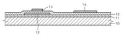
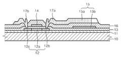
도 1a 내지 도 1g는 본 발명의 일 실시예에 따른 박막 트랜지스터의 제조방법을 개략적으로 도시하는 단면도들이다.1A to 1G are cross-sectional views schematically illustrating a method of manufacturing a thin film transistor according to an exemplary embodiment of the present invention.
먼저 도 1a에 도시된 것과 같이 상면에 버퍼층(11)이 형성된 기판(10) 상에 활성층(12)을 형성한다.First, as shown in FIG. 1A, the
기판(10)으로는 글라스재 기판뿐만 아니라 아크릴과 같은 다양한 플라스틱재 기판을 사용할 수도 있다. 상기 기판(10) 상에 박막 트랜지스터를 형성하고 그 상부에 디스플레이 소자를 형성한 후 박막 트랜지스터를 통하여 외부로 광이 취출되도록 할 경우에는 한 기판을 이용할 수도 있다. 물론, 기판(10) 상에 박막 트랜지스터를 형성하고 그 상부에 디스플레이 소자를 형성한 후 기판(10)으로 금속과 같 은 반사성 기판을 이용할 수도 있는데, 이 경우에는 디스플레이 소자와 기판 사이에서 광이 박막 트랜지스터를 통과하여 광공진이 일어나도록 할 수도 있는 등 다양한 목적을 위한 다양한 변형이 가능하다.As the
상기 버퍼층(11) 상에 패터닝된 활성층(12)을 형성한다. 이러한 활성층(12)은 반도체재인 산화물로 형성될 수 있는데, 구체적으로는 ZnO, InZnO, ZnSnO 또는 ZnInGaO와 같은 ZnO를 포함하는 물질로 형성될 수 있다. 물론 본 발명이 이에 한정되는 것은 아니며, 이 외의 반도체 특성을 갖는 다양한 물질을 이용할 수 있다. 이러한 패터닝된 활성층(12)은 마스크를 이용한 증착 등을 통하여 도 1a에 도시된 것과 같이 패터닝된 형태로 형성될 수도 있고, 이와 달리 기판(10)의 전면에 대응하도록 반도체재를 형성한 후 이를 패터닝하여 형성될 수도 있다.The patterned
활성층(12)을 형성한 후, 도 1b에 도시된 바와 같이 이 활성층(12) 상에 게이트 절연막(13)을 형성한다. After the
게이트 절연막(13)은 다양한 물질로 형성될 수 있는데, 절연성을 가진 파릴렌(parylene) 또는 에폭시(epoxy) 등과 같은 유기물을 이용할 수 있다. 물론 이 게이트 절연막(13)은 무기물로 형성될 수도 있으며, 또한 게이트 절연막(13)이 할 필요가 있을 경우에는 실리콘 옥사이드 또는 실리콘 나이트라이드 등과 같은 재료를 이용할 수도 있다.The
다음, 게이트 절연막(13) 위에 게이트 전극(14)과 캐패시터의 하부 전극(15)을 형성한다. 게이트 전극(14)과 캐패시터 하부 전극(15)은 Al, Mo, W, Cr, Ni 또는 이들의 화합물과 같은 다양한 도전성 재료로 형성될 수 있다. 물론 박막 트랜 지스터의 활성층 외에 다른 구성요소까지도 광이 통과할 필요성이 있을 경우에는, 게이트 전극(14) 및 캐패시터 하부 전극(15)이 ITO 또는 IZO 등과 같은 다양한 도전성 재료로 형성될 수 있다. 이러한 게이트 전극(15) 및 캐패시터 하부 전극(15)은 단일층 또는 다층으로 구비될 수 있다.Next, the
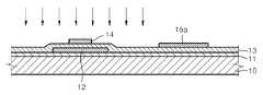
이렇게 게이트 전극(14)까지 형성한 이후, 도 1b에서 볼 수 있듯이, 게이트 전극(14)을 셀프 얼라인(self-align) 마스크로 하여 활성층(12)에 수소 이온의 임플란트를 행한다. 즉, 게이트 전극(14)이 활성층(12)의 채널 영역을 가리는 상태가 되기 때문에, 수소 이온의 임플란트 시 활성층(12)의 소스 및 드레인 영역이 이온 도핑될 수 있게 된다.After forming the
이 때의 수소 도우즈(dose)의 양은 1e16/㎠이상 1e18/㎠이하가 되도록 하고, 수소 이온 주입 에너지는 50keV이상 150keV이하가 되도록 한다.수소 도우즈의 양이 1e16/㎠보다 낮을 경우, 접촉저항 개선효과가 낮게 되고, 수소 도우즈의 양이 1e18/㎠보다 높을 경우 고용한계(solubility limit)를 넘게 되어 도핑 효율이 감소하게 된다. 수소 이온 주입 에너지가 50keV보다 낮을 경우 표면부터 도우즈의 투사깊이가 작아지는 문제가 있고, 150keV보다 클 경우 평균 이온주입장비의 가격이 상승하는 문제가 있게 된다.At this time, the amount of hydrogen dose is 1e16 / cm 2 or more and 1e18 / cm 2 or less, and the hydrogen ion implantation energy is 50keV or more and 150keV or less.If the amount of hydrogen doseis lower than1e16/ ㎠, the effect of improving the contact resistance is low, and if the amount of hydrogen doseis higher than1e18/ ㎠ it exceeds the solubility limit to reduce the doping efficiency. . When the hydrogen ion implantation energy is lower than 50 keV, the projection depth of the dose is reduced from the surface, and when larger than 150 keV, the price of the average ion implantation equipment increases.
이에 따라 도 1e에서 볼 수 있듯이, 활성층(12)의 소스 영역(12b) 및 드레인 영역(12c)이 오믹 콘택을 위한 n+층이 되도록 할 수 있다.Accordingly, as shown in FIG. 1E, the
이에 따라 소스 영역(12b) 및 드레인 영역(12c)에는 수소 농도가 1018/㎤이상 1021/㎤이하가 되도록 할 수 있다.소스 영역(12b) 및 드레인 영역(12c)의 수소 농도가 1018/㎤보다 낮을 경우, 접촉저항 개선효과가 낮게 되고, 1021/㎤보다 높을 경우 고용한계(solubility limit)를 넘게 되어 도핑 효율이 감소하게 된다.Accordingly, the hydrogen concentration in the
본 발명의 경우, 상기와 같이 수소 이온 임플란트를 행한 이후에 별다른 액티베이션(activation) 공정을 거치지 않아도 무방하다.In the case of the present invention, after performing the hydrogen ion implant as described above, there is no need to go through a different activation process.
따라서, 본 발명은 고온 열처리 공정이 불가능한 플라스틱제 기판에 적용하기에 충분하다.Therefore, the present invention is sufficient for application to plastic substrates in which high temperature heat treatment processes are impossible.
수소 이온의 임플란트를 행한 후에 액티베이션 공정을 거치는 경우에도 200℃ 이하의 저온 열처리 만으로도 충분하게 액티베이션 효과를 올릴 수 있다. 따라서, 열처리를 행한다 하더라도 플라스틱 기판에 충분히 적용할 수 있다.Even when the activation process is performed after the implantation of hydrogen ions, a low temperature heat treatment of 200 ° C. or lower can sufficiently increase the activation effect. Therefore, even if heat processing is performed, it can fully apply to a plastic substrate.
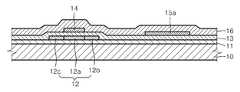
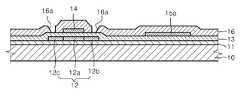
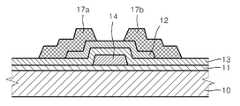
상기와 같이 수소 이온의 주입 공정이 끝난 후에는 도1e에서 볼 수 있듯이, 게이트 전극(14) 및 캐패시터 하부 전극(15a)을 덮도록 층간 절연막(16)을 형성한 후, 도 1f에서 볼 수 있도록 이 층간 절연막(16)에 콘택 홀(16a)을 형성한 후, 도 1g에서 볼 수 있도록 층간 절연막(16) 상에 소스 전극(17a) 및 드레인 전극(17b)을 형성한다. 소스 전극(17a)의 형성 시에 이 소스 전극(17a)과 일체가 되도록 캐패시터(15)의 상부 전극(15b)을 형성한다.After the implantation process of hydrogen ions is completed, as shown in FIG. 1E, the
상기 소스 전극(17a) 및 드레인 전극(17b)과 캐패시터(15)의 상부 전극(15b)은 Al, Mo, W, Cr, Ni 또는 이들의 화합물, ITO 또는 IZO 등과 같은 도전물질 등 의 다양한 도전성 재료로 단일층 또는 다층으로 구비될 수 있다.The
이렇게 하여 박막 트랜지스터를 제조한 후에는 상기 드레인 전극(17b)에 콘택되도록 유기 발광 소자를 더 적층 형성하여, 유기 발광 표시장치로서 형성할 수 있다.After the thin film transistor is manufactured in this manner, an organic light emitting diode may be further stacked to contact the
이 경우, 박막 트랜지스터의 활성층(12)이 하므로, 기판(10)의 방향으로 발광이 이루어지는 배면 발광형에 적용하기에도 무방하다.In this case, since the
다음으로, 도 2a 내지 도 2i는 본 발명의 다른 일 실시예에 따른 박막 트랜지스터의 제조방법을 순차로 도시한 것이다. 도면에 도시된 부호는 도1a 내지 도 1g의 부재와 동일한 부재에 대해서는 동일 부호로서 도시하였다.Next, FIGS. 2A to 2I sequentially illustrate a method of manufacturing a thin film transistor according to another exemplary embodiment of the present invention. Reference numerals shown in the drawings are shown as the same reference numerals for the same members as those in Figs.
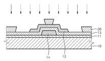
먼저 도 2a에 도시된 것과 같이 기판(10) 상에 게이트 전극(14)을 형성한다.기판(10)상에는 전술한 바와 같이 버퍼층(11)이 더 형성되어 있다.First, as shown in FIG. 2A, the
게이트 전극(14)을 형성한 후, 도 2b에 도시된 바와 같이 이 게이트 전극(14) 상에 게이트 절연막(13)을 형성한다. 도 2b에서는 게이트 절연막(13)이 게이트 전극(14)을 덮는 것으로 도시되어 있으나, 본 실시예에 따른 제조방법이 이에 한정되는 것은 아니다.After the
게이트 절연막(13)을 형성한 후, 도 2c에 도시된 것과 같이 게이트 절연막(13) 상에 패터닝된 활성층(12)을 형성한다. 이러한 활성층(12)은 전술한 바와 같이, 산화물 반도체재로 형성될 수 있다.After the
활성층(12)을 형성한 후, 이 활성층(12)의 소스 영역과 드레인 영역이 노출되도록 활성층(12) 상에 포토리지스트층을 형성한다. 이를 상세히 설명하면, 먼 저 도 2d에 도시된 것과 같이 기판(10)의 전면에 대응하도록 포토리지스트층(30)을 형성하고, 그 후 도 2e에 도시된 것과 같이 활성층(12)의 소스 영역(12b)과 드레인 영역(12c)이 노출되도록 포토리지스트층(30)을 패터닝한다. 이러한 포토리지스트층(30)의 패터닝은 통상적인 포토리소그래피법을 이용하여 이루어질 수 있다. After the
그 후, 도 2f에 도시된 것과 같이 패터닝된 포토리지스트층(30)을 마스크로 이용하여 활성층(12)의 채널 영역(12a)을 가린 상태에서, 노출된 소스 영역(12b)과 드레인 영역(12c)에 대해 수소 이온 임플란트를 행한다. 이 때, 포토리지스트층(30)의 형성 전에 층간 절연막(미도시)을 더 형성한 후, 포토리지스트층(30)을 전술한 바와 같이 형성, 패터닝하여도 무방하다. 수소 이온의 임플란트에 대해서는 전술한 바와 동일하므로 상세한 설명은 생략한다.Thereafter, as shown in FIG. 2F, using the patterned
다음으로, 도 2g에 도시된 것과 같이 기판(10)의 전면(全面)에 대응하도록 도전층(17)을 형성한다. 이때 패터닝된 포토리지스트층(30)이 존재하기 때문에 도전층(17)은 기판(10)의 전면에 있어서 모두 일체로 형성되는 것이 아니라, 포토리지스트층(30) 상에 형성되기도 하고 활성층(12)의 노출된 소스 영역과 드레인 영역 상에 형성되기도 한다. 이때 포토리지스트층(30)의 단차에 의하여, 활성층(12)의 노출된 소스 영역과 드레인 영역 상에 형성된 도전층과 포토리지스트층(30) 상에 형성된 도전층은 도 2g에 도시된 것과 같이 서로 분리된다. 이러한 도전층(17)은 Al, Mo, W, Cr, Ni 또는 이들의 화합물, ITO 또는 IZO 등과 같은 도전물질 등의 다양한 도전성 재료로 단일층 또는 다층으로 구비될 수 있다.Next, as shown in FIG. 2G, the
그 후 포토리지스트층(30)을 리프트-오프(lift-off)법을 이용하여 제거함으 로써, 도 2h에 도시된 것과 같이 도전층이 패터닝되도록, 즉 활성층(12)의 소스 영역에 접하는 소스 전극(17a)과 활성층(12)의 드레인 영역에 접하는 드레인 전극(17b)을 형성한다.The
위 실시예에서는 이와 같이 활성층(12)의 소스 영역 및 드레인 영역을 수소 이온으로 임플란트하기 위하여 포토리지스트층을 형성하였는 바, 이 포토리지스트층은 결과적으로 소스 전극(17a)과 드레인 전극(17b)을 형성하기 위해서도 사용된다. 따라서 반도체층을 도핑하기 위한 공정과 소스 전극 및 드레인 전극을 형성하기 위한 공정에서 각각 별도로 패터닝 공정을 거치거나 각각 별도의 마스크 공정을 거쳐야만 했던 종래의 제조방법과 달리, 포토리지스트층의 패터닝이라는 한 번의 패터닝 공정 또는 한번의 마스크 공정만을 거치게 된다. 따라서 제조비용이 절감되고 수율을 향상시킬 수 있다.In the above embodiment, a photoresist layer is formed to implant the source region and the drain region of the
상기한 바와 같이 이루어진 본 발명의 박막 트랜지스터의 제조방법에 따르면, 소스 전극 및 드레인 전극과 활성층 사이의 오믹 컨택을 이룰 수 있는 박막 트랜지스터를 제공할 수 있다.According to the manufacturing method of the thin film transistor of the present invention made as described above, it is possible to provide a thin film transistor capable of making an ohmic contact between the source electrode and the drain electrode and the active layer.
본 발명은 도면에 도시된 실시예를 참고로 설명되었으나 이는 예시적인 것에 불과하며, 당해 기술 분야에서 통상의 지식을 가진 자라면 이로부터 다양한 변형 및 균등한 다른 실시예가 가능하다는 점을 이해할 것이다. 따라서, 본 발명의 진정한 기술적 보호 범위는 첨부된 특허청구범위의 기술적 사상에 의하여 정해져야 할 것이다.Although the present invention has been described with reference to the embodiments shown in the drawings, these are merely exemplary, and those skilled in the art will understand that various modifications and equivalent other embodiments are possible. Therefore, the true technical protection scope of the present invention will be defined by the technical spirit of the appended claims.
Claims (12)
Translated fromKoreanPriority Applications (3)
| Application Number | Priority Date | Filing Date | Title |
|---|---|---|---|
| KR1020070002172AKR100787464B1 (en) | 2007-01-08 | 2007-01-08 | Thin film transistor, and manufacturing method thereof |
| US11/763,373US8698215B2 (en) | 2007-01-08 | 2007-06-14 | Transparent thin film transistor, and method of manufacturing the same |
| US14/168,967US20140145188A1 (en) | 2007-01-08 | 2014-01-30 | Transparent thin film transistor, and method of manufacturing the same |
Applications Claiming Priority (1)
| Application Number | Priority Date | Filing Date | Title |
|---|---|---|---|
| KR1020070002172AKR100787464B1 (en) | 2007-01-08 | 2007-01-08 | Thin film transistor, and manufacturing method thereof |
Publications (1)
| Publication Number | Publication Date |
|---|---|
| KR100787464B1true KR100787464B1 (en) | 2007-12-26 |
Family
ID=39147568
Family Applications (1)
| Application Number | Title | Priority Date | Filing Date |
|---|---|---|---|
| KR1020070002172AActiveKR100787464B1 (en) | 2007-01-08 | 2007-01-08 | Thin film transistor, and manufacturing method thereof |
Country Status (2)
| Country | Link |
|---|---|
| US (2) | US8698215B2 (en) |
| KR (1) | KR100787464B1 (en) |
Cited By (5)
| Publication number | Priority date | Publication date | Assignee | Title |
|---|---|---|---|---|
| US8638030B2 (en) | 2010-01-05 | 2014-01-28 | Samsung Display Co., Ltd. | Organic light emitting display device including pixel electrode not formed in light transmissive region |
| KR101493305B1 (en) | 2008-07-31 | 2015-02-13 | 가부시키가이샤 한도오따이 에네루기 켄큐쇼 | Method for manufacturing semiconductor device |
| KR101561924B1 (en) | 2014-06-12 | 2015-10-22 | 연세대학교 산학협력단 | Method for post-treating oxide thin film, and method for fabricating semiconductor device using the same |
| KR101611908B1 (en)* | 2009-11-11 | 2016-04-12 | 엘지디스플레이 주식회사 | Thin Film Transistor Array Substrate and Method for Manufacturing the Same |
| US10205030B2 (en) | 2008-08-08 | 2019-02-12 | Semiconductor Energy Laboratory Co., Ltd. | Method for manufacturing semiconductor device |
Families Citing this family (21)
| Publication number | Priority date | Publication date | Assignee | Title |
|---|---|---|---|---|
| JP5105842B2 (en) | 2006-12-05 | 2012-12-26 | キヤノン株式会社 | Display device using oxide semiconductor and manufacturing method thereof |
| JP5616012B2 (en)* | 2008-10-24 | 2014-10-29 | 株式会社半導体エネルギー研究所 | Method for manufacturing semiconductor device |
| EP2515337B1 (en) | 2008-12-24 | 2016-02-24 | Semiconductor Energy Laboratory Co., Ltd. | Driver circuit and semiconductor device |
| KR101097454B1 (en)* | 2009-02-16 | 2011-12-23 | 네오뷰코오롱 주식회사 | Pixel circuit for organic light emitting diode(oled) panel, display device having the same, and method of driving oled panel using the same |
| US20100224880A1 (en)* | 2009-03-05 | 2010-09-09 | Semiconductor Energy Laboratory Co., Ltd. | Semiconductor device |
| US8012773B2 (en)* | 2009-06-11 | 2011-09-06 | Canon Kabushiki Kaisha | Method for manufacturing liquid discharge head |
| KR101751908B1 (en)* | 2009-10-21 | 2017-06-28 | 가부시키가이샤 한도오따이 에네루기 켄큐쇼 | Voltage regulator circuit |
| KR102393447B1 (en) | 2009-11-13 | 2022-05-03 | 가부시키가이샤 한도오따이 에네루기 켄큐쇼 | Semiconductor device and manufacturing method thereof |
| TW201133857A (en)* | 2010-03-26 | 2011-10-01 | Prime View Int Co Ltd | Oxide thin film transistor, display device, and method for manufacturing same |
| CN102237411A (en)* | 2010-05-05 | 2011-11-09 | 元太科技工业股份有限公司 | Oxide thin film transistor and manufacturing method thereof |
| US9473714B2 (en)* | 2010-07-01 | 2016-10-18 | Semiconductor Energy Laboratory Co., Ltd. | Solid-state imaging device and semiconductor display device |
| WO2012002197A1 (en)* | 2010-07-02 | 2012-01-05 | Semiconductor Energy Laboratory Co., Ltd. | Liquid crystal display device |
| KR101824125B1 (en)* | 2010-09-10 | 2018-02-01 | 가부시키가이샤 한도오따이 에네루기 켄큐쇼 | Display device |
| TWI535014B (en)* | 2010-11-11 | 2016-05-21 | 半導體能源研究所股份有限公司 | Semiconductor device and method of manufacturing same |
| JP6013685B2 (en)* | 2011-07-22 | 2016-10-25 | 株式会社半導体エネルギー研究所 | Semiconductor device |
| TW201322341A (en)* | 2011-11-21 | 2013-06-01 | Ind Tech Res Inst | Semiconductor component and method of manufacturing the same |
| CN108054175A (en) | 2012-08-03 | 2018-05-18 | 株式会社半导体能源研究所 | Semiconductor device |
| KR102241249B1 (en) | 2012-12-25 | 2021-04-15 | 가부시키가이샤 한도오따이 에네루기 켄큐쇼 | Resistor, display device, and electronic device |
| KR102680781B1 (en) | 2012-12-25 | 2024-07-04 | 가부시키가이샤 한도오따이 에네루기 켄큐쇼 | Semiconductor device |
| KR102660292B1 (en)* | 2016-06-23 | 2024-04-24 | 삼성디스플레이 주식회사 | Thin film transistor array panel and manufacturing method thereof |
| US11444204B2 (en)* | 2018-03-28 | 2022-09-13 | Intel Corporation | Transistor device with channel recess structure and method of providing same |
Citations (6)
| Publication number | Priority date | Publication date | Assignee | Title |
|---|---|---|---|---|
| KR20010015419A (en)* | 1999-07-22 | 2001-02-26 | 야마자끼 순페이 | Contact structure and semiconductor device |
| KR20010014785A (en)* | 1999-04-20 | 2001-02-26 | 야마자끼 순페이 | Semiconductor device and manufacturing method thereof |
| KR20030004111A (en)* | 2001-07-02 | 2003-01-14 | 가부시키가이샤 한도오따이 에네루기 켄큐쇼 | Semiconductor device and method of manufacturing the same |
| JP2005033172A (en)* | 2003-06-20 | 2005-02-03 | Sharp Corp | Semiconductor device, manufacturing method thereof, and electronic device |
| KR20060001322A (en)* | 2004-06-30 | 2006-01-06 | 삼성에스디아이 주식회사 | Thin film transistor, and flat panel display device having same |
| KR20070069187A (en)* | 2004-10-20 | 2007-07-02 | 가부시키가이샤 한도오따이 에네루기 켄큐쇼 | Laser irradiation method, laser irradiation device, and semiconductor device manufacturing method |
Family Cites Families (8)
| Publication number | Priority date | Publication date | Assignee | Title |
|---|---|---|---|---|
| US5834827A (en)* | 1994-06-15 | 1998-11-10 | Seiko Epson Corporation | Thin film semiconductor device, fabrication method thereof, electronic device and its fabrication method |
| US6716768B2 (en)* | 2000-02-15 | 2004-04-06 | Matsushita Electric Industrial Co., Ltd. | Method of manufacturing thin-film transistor, and liquid-crystal display |
| TWI247182B (en)* | 2000-09-29 | 2006-01-11 | Toshiba Corp | Flat panel display device and method for manufacturing the same |
| US7244627B2 (en)* | 2003-08-25 | 2007-07-17 | Lg.Philips Lcd Co., Ltd. | Method for fabricating liquid crystal display device |
| TWI221341B (en)* | 2003-09-18 | 2004-09-21 | Ind Tech Res Inst | Method and material for forming active layer of thin film transistor |
| AU2005302964B2 (en)* | 2004-11-10 | 2010-11-04 | Canon Kabushiki Kaisha | Field effect transistor employing an amorphous oxide |
| KR100953596B1 (en)* | 2004-11-10 | 2010-04-21 | 캐논 가부시끼가이샤 | Light emitting device |
| US20060240275A1 (en)* | 2005-04-25 | 2006-10-26 | Gadkaree Kishor P | Flexible display substrates |
- 2007
- 2007-01-08KRKR1020070002172Apatent/KR100787464B1/enactiveActive
- 2007-06-14USUS11/763,373patent/US8698215B2/enactiveActive
- 2014
- 2014-01-30USUS14/168,967patent/US20140145188A1/ennot_activeAbandoned
Patent Citations (6)
| Publication number | Priority date | Publication date | Assignee | Title |
|---|---|---|---|---|
| KR20010014785A (en)* | 1999-04-20 | 2001-02-26 | 야마자끼 순페이 | Semiconductor device and manufacturing method thereof |
| KR20010015419A (en)* | 1999-07-22 | 2001-02-26 | 야마자끼 순페이 | Contact structure and semiconductor device |
| KR20030004111A (en)* | 2001-07-02 | 2003-01-14 | 가부시키가이샤 한도오따이 에네루기 켄큐쇼 | Semiconductor device and method of manufacturing the same |
| JP2005033172A (en)* | 2003-06-20 | 2005-02-03 | Sharp Corp | Semiconductor device, manufacturing method thereof, and electronic device |
| KR20060001322A (en)* | 2004-06-30 | 2006-01-06 | 삼성에스디아이 주식회사 | Thin film transistor, and flat panel display device having same |
| KR20070069187A (en)* | 2004-10-20 | 2007-07-02 | 가부시키가이샤 한도오따이 에네루기 켄큐쇼 | Laser irradiation method, laser irradiation device, and semiconductor device manufacturing method |
Cited By (10)
| Publication number | Priority date | Publication date | Assignee | Title |
|---|---|---|---|---|
| KR101493305B1 (en) | 2008-07-31 | 2015-02-13 | 가부시키가이샤 한도오따이 에네루기 켄큐쇼 | Method for manufacturing semiconductor device |
| US9087745B2 (en) | 2008-07-31 | 2015-07-21 | Semiconductor Energy Laboratory Co., Ltd. | Semiconductor device and method for manufacturing the same |
| US9111804B2 (en) | 2008-07-31 | 2015-08-18 | Semiconductor Energy Laboratory Co., Ltd. | Semiconductor device and method for manufacturing the same |
| US10937897B2 (en) | 2008-07-31 | 2021-03-02 | Semiconductor Energy Laboratory Co., Ltd. | Semiconductor device and method for manufacturing the same |
| US12074210B2 (en) | 2008-07-31 | 2024-08-27 | Semiconductor Energy Laboratory Co., Ltd. | Semiconductor device and method for manufacturing the same |
| US10205030B2 (en) | 2008-08-08 | 2019-02-12 | Semiconductor Energy Laboratory Co., Ltd. | Method for manufacturing semiconductor device |
| KR101611908B1 (en)* | 2009-11-11 | 2016-04-12 | 엘지디스플레이 주식회사 | Thin Film Transistor Array Substrate and Method for Manufacturing the Same |
| US8638030B2 (en) | 2010-01-05 | 2014-01-28 | Samsung Display Co., Ltd. | Organic light emitting display device including pixel electrode not formed in light transmissive region |
| KR101561924B1 (en) | 2014-06-12 | 2015-10-22 | 연세대학교 산학협력단 | Method for post-treating oxide thin film, and method for fabricating semiconductor device using the same |
| US9484419B2 (en) | 2014-06-12 | 2016-11-01 | Industry-Academic Cooperation Foundation, Yonsei University | Oxide thin film, method for post-treating oxide thin film and electronic apparatus |
Also Published As
| Publication number | Publication date |
|---|---|
| US20080166475A1 (en) | 2008-07-10 |
| US8698215B2 (en) | 2014-04-15 |
| US20140145188A1 (en) | 2014-05-29 |
Similar Documents
| Publication | Publication Date | Title |
|---|---|---|
| KR100787464B1 (en) | Thin film transistor, and manufacturing method thereof | |
| US8399274B2 (en) | Organic light emitting display and method of manufacturing the same | |
| JP5498177B2 (en) | THIN FILM TRANSISTOR, ITS MANUFACTURING METHOD, AND ORGANIC ELECTROLUMINESCENT DISPLAY | |
| US9059432B2 (en) | Organic light emitting display device and method for fabricating the same | |
| US9768323B2 (en) | Manufacture method of dual gate oxide semiconductor TFT substrate and structure thereof | |
| CN103021820B (en) | Manufacture the method for thin-film transistor and manufacture the method for oganic light-emitting display device | |
| US9437627B2 (en) | Thin film transistor and manufacturing method thereof | |
| US9543442B2 (en) | Manufacture method of dual gate oxide semiconductor TFT substrate and structure thereof | |
| CN107681063B (en) | Array substrate and preparation method thereof, and display device | |
| CN103730510B (en) | A kind of thin film transistor (TFT) and preparation method thereof, array base palte, display device | |
| CN109037343B (en) | A double-layer channel thin film transistor and preparation method thereof, and display panel | |
| WO2016008226A1 (en) | Thin film transistor and preparation method for same, array substrate and display device | |
| CN102403313B (en) | Semiconductor element and manufacturing method thereof | |
| KR20140139773A (en) | Flat panel display device having oxide thin film transistor and method for fabricating thereof | |
| CN105097841A (en) | TFT substrate and manufacturing method thereof | |
| CN105097552A (en) | Manufacturing methods of thin film transistor and array substrate, array substrate and display device | |
| US9419029B1 (en) | Method for manufacturing thin film transistor array substrate and thin film transistor array substrate for the same | |
| JP3748827B2 (en) | Organic EL display device manufacturing method | |
| KR102060377B1 (en) | A Display device, method of fabricating the same, and method of fabricating an image sensor device | |
| KR20150026322A (en) | Display substrate and method of manufacturing a display substrate | |
| CN102339835A (en) | Semiconductor component, electroluminescent component and manufacturing method thereof | |
| CN107819012A (en) | N-type TFT and preparation method thereof, OLED display panel and preparation method thereof | |
| US10361226B2 (en) | Array substrate, manufacturing method for the same and display panel | |
| KR100982314B1 (en) | Thin film transistor, manufacturing method thereof and organic light emitting display device comprising same | |
| US20190221672A1 (en) | Low temperature polysilicon thin film transistor and preparation method thereof |
Legal Events
| Date | Code | Title | Description |
|---|---|---|---|
| A201 | Request for examination | ||
| PA0109 | Patent application | Patent event code:PA01091R01D Comment text:Patent Application Patent event date:20070108 | |
| PA0201 | Request for examination | ||
| E701 | Decision to grant or registration of patent right | ||
| PE0701 | Decision of registration | Patent event code:PE07011S01D Comment text:Decision to Grant Registration Patent event date:20071126 | |
| GRNT | Written decision to grant | ||
| PR0701 | Registration of establishment | Comment text:Registration of Establishment Patent event date:20071213 Patent event code:PR07011E01D | |
| PR1002 | Payment of registration fee | Payment date:20071214 End annual number:3 Start annual number:1 | |
| PG1601 | Publication of registration | ||
| PR1001 | Payment of annual fee | Payment date:20101129 Start annual number:4 End annual number:4 | |
| PR1001 | Payment of annual fee | Payment date:20111129 Start annual number:5 End annual number:5 | |
| FPAY | Annual fee payment | Payment date:20121130 Year of fee payment:6 | |
| PR1001 | Payment of annual fee | Payment date:20121130 Start annual number:6 End annual number:6 | |
| FPAY | Annual fee payment | Payment date:20131129 Year of fee payment:7 | |
| PR1001 | Payment of annual fee | Payment date:20131129 Start annual number:7 End annual number:7 | |
| FPAY | Annual fee payment | Payment date:20141128 Year of fee payment:8 | |
| PR1001 | Payment of annual fee | Payment date:20141128 Start annual number:8 End annual number:8 | |
| FPAY | Annual fee payment | Payment date:20181126 Year of fee payment:12 | |
| PR1001 | Payment of annual fee | Payment date:20181126 Start annual number:12 End annual number:12 | |
| FPAY | Annual fee payment | Payment date:20191202 Year of fee payment:13 | |
| PR1001 | Payment of annual fee | Payment date:20191202 Start annual number:13 End annual number:13 | |
| PR1001 | Payment of annual fee | Payment date:20201201 Start annual number:14 End annual number:14 | |
| PR1001 | Payment of annual fee | Payment date:20211125 Start annual number:15 End annual number:15 | |
| PR1001 | Payment of annual fee | Payment date:20241125 Start annual number:18 End annual number:18 |