KR100787463B1 - Glass frit, composition for forming sealing material, light emitting device and manufacturing method of light emitting device - Google Patents
Glass frit, composition for forming sealing material, light emitting device and manufacturing method of light emitting deviceDownload PDFInfo
- Publication number
- KR100787463B1 KR100787463B1KR1020070001681AKR20070001681AKR100787463B1KR 100787463 B1KR100787463 B1KR 100787463B1KR 1020070001681 AKR1020070001681 AKR 1020070001681AKR 20070001681 AKR20070001681 AKR 20070001681AKR 100787463 B1KR100787463 B1KR 100787463B1
- Authority
- KR
- South Korea
- Prior art keywords
- ions
- sealing material
- light emitting
- composition
- emitting device
- Prior art date
- Legal status (The legal status is an assumption and is not a legal conclusion. Google has not performed a legal analysis and makes no representation as to the accuracy of the status listed.)
- Active
Links
- 239000003566sealing materialSubstances0.000titleclaimsabstractdescription179
- 239000000203mixtureSubstances0.000titleclaimsabstractdescription125
- 239000011521glassSubstances0.000titleclaimsabstractdescription99
- 238000004519manufacturing processMethods0.000titleclaimsabstractdescription19
- 150000002500ionsChemical class0.000claimsabstractdescription336
- 239000000758substrateSubstances0.000claimsabstractdescription108
- 238000000034methodMethods0.000claimsabstractdescription62
- 238000007789sealingMethods0.000claimsabstractdescription19
- 239000000945fillerSubstances0.000claimsdescription73
- 239000003638chemical reducing agentSubstances0.000claimsdescription32
- 238000010438heat treatmentMethods0.000claimsdescription30
- 239000011701zincSubstances0.000claimsdescription26
- 239000002245particleSubstances0.000claimsdescription23
- 239000011347resinSubstances0.000claimsdescription22
- 229920005989resinPolymers0.000claimsdescription22
- 239000012298atmosphereSubstances0.000claimsdescription20
- RWWJXIAEEFWUSU-UHFFFAOYSA-KP(=O)([O-])([O-])[O-].[W+4].[Zr+4]Chemical compoundP(=O)([O-])([O-])[O-].[W+4].[Zr+4]RWWJXIAEEFWUSU-UHFFFAOYSA-K0.000claimsdescription13
- VYPSYNLAJGMNEJ-UHFFFAOYSA-NSilicium dioxideChemical compoundO=[Si]=OVYPSYNLAJGMNEJ-UHFFFAOYSA-N0.000claimsdescription13
- 229910052749magnesiumInorganic materials0.000claimsdescription10
- 229910052726zirconiumInorganic materials0.000claimsdescription10
- 229910052718tinInorganic materials0.000claimsdescription9
- QCWXUUIWCKQGHC-UHFFFAOYSA-NZirconiumChemical compound[Zr]QCWXUUIWCKQGHC-UHFFFAOYSA-N0.000claimsdescription8
- 229910052782aluminiumInorganic materials0.000claimsdescription8
- 230000015572biosynthetic processEffects0.000claimsdescription8
- -1ion ionChemical class0.000claimsdescription8
- 229910000166zirconium phosphateInorganic materials0.000claimsdescription8
- LEHFSLREWWMLPU-UHFFFAOYSA-Bzirconium(4+);tetraphosphateChemical compound[Zr+4].[Zr+4].[Zr+4].[O-]P([O-])([O-])=O.[O-]P([O-])([O-])=O.[O-]P([O-])([O-])=O.[O-]P([O-])([O-])=OLEHFSLREWWMLPU-UHFFFAOYSA-B0.000claimsdescription8
- 239000003822epoxy resinSubstances0.000claimsdescription7
- 229920000647polyepoxidePolymers0.000claimsdescription7
- 239000004925Acrylic resinSubstances0.000claimsdescription6
- 229920000178Acrylic resinPolymers0.000claimsdescription6
- OKTJSMMVPCPJKN-UHFFFAOYSA-NCarbonChemical compound[C]OKTJSMMVPCPJKN-UHFFFAOYSA-N0.000claimsdescription6
- 229910052799carbonInorganic materials0.000claimsdescription6
- 229910052802copperInorganic materials0.000claimsdescription6
- LNEPOXFFQSENCJ-UHFFFAOYSA-NhaloperidolChemical compoundC1CC(O)(C=2C=CC(Cl)=CC=2)CCN1CCCC(=O)C1=CC=C(F)C=C1LNEPOXFFQSENCJ-UHFFFAOYSA-N0.000claimsdescription6
- 230000001678irradiating effectEffects0.000claimsdescription6
- 125000005641methacryl groupChemical group0.000claimsdescription6
- 230000003287optical effectEffects0.000claimsdescription6
- 239000000377silicon dioxideSubstances0.000claimsdescription6
- 239000002904solventSubstances0.000claimsdescription6
- 229920002803thermoplastic polyurethanePolymers0.000claimsdescription6
- RBNWAMSGVWEHFP-UHFFFAOYSA-Ntrans-p-Menthane-1,8-diolChemical compoundCC(C)(O)C1CCC(C)(O)CC1RBNWAMSGVWEHFP-UHFFFAOYSA-N0.000claimsdescription6
- 125000000391vinyl groupChemical group[H]C([*])=C([H])[H]0.000claimsdescription6
- 229920002554vinyl polymerPolymers0.000claimsdescription6
- 229910052725zincInorganic materials0.000claimsdescription6
- OAYXUHPQHDHDDZ-UHFFFAOYSA-N2-(2-butoxyethoxy)ethanolChemical compoundCCCCOCCOCCOOAYXUHPQHDHDDZ-UHFFFAOYSA-N0.000claimsdescription5
- VXQBJTKSVGFQOL-UHFFFAOYSA-N2-(2-butoxyethoxy)ethyl acetateChemical compoundCCCCOCCOCCOC(C)=OVXQBJTKSVGFQOL-UHFFFAOYSA-N0.000claimsdescription5
- 229910000505Al2TiO5Inorganic materials0.000claimsdescription5
- 239000004110Zinc silicateSubstances0.000claimsdescription5
- PNEYBMLMFCGWSK-UHFFFAOYSA-Naluminium oxideInorganic materials[O-2].[O-2].[O-2].[Al+3].[Al+3]PNEYBMLMFCGWSK-UHFFFAOYSA-N0.000claimsdescription5
- AABBHSMFGKYLKE-SNAWJCMRSA-Npropan-2-yl (e)-but-2-enoateChemical compoundC\C=C\C(=O)OC(C)CAABBHSMFGKYLKE-SNAWJCMRSA-N0.000claimsdescription5
- XSMMCTCMFDWXIX-UHFFFAOYSA-Nzinc silicateChemical compound[Zn+2].[O-][Si]([O-])=OXSMMCTCMFDWXIX-UHFFFAOYSA-N0.000claimsdescription5
- 235000019352zinc silicateNutrition0.000claimsdescription5
- CKQGKSPXCTWTCX-UHFFFAOYSA-Nbutanoic acid;2,2,4-trimethylpentane-1,3-diolChemical compoundCCCC(O)=O.CC(C)C(O)C(C)(C)COCKQGKSPXCTWTCX-UHFFFAOYSA-N0.000claimsdescription4
- 239000012461cellulose resinSubstances0.000claimsdescription4
- 229910052878cordieriteInorganic materials0.000claimsdescription4
- JSKIRARMQDRGJZ-UHFFFAOYSA-Ndimagnesium dioxido-bis[(1-oxido-3-oxo-2,4,6,8,9-pentaoxa-1,3-disila-5,7-dialuminabicyclo[3.3.1]nonan-7-yl)oxy]silaneChemical compound[Mg++].[Mg++].[O-][Si]([O-])(O[Al]1O[Al]2O[Si](=O)O[Si]([O-])(O1)O2)O[Al]1O[Al]2O[Si](=O)O[Si]([O-])(O1)O2JSKIRARMQDRGJZ-UHFFFAOYSA-N0.000claimsdescription4
- 230000005496eutecticsEffects0.000claimsdescription4
- 238000002360preparation methodMethods0.000claimsdescription3
- 238000007669thermal treatmentMethods0.000claims1
- 229910052720vanadiumInorganic materials0.000claims1
- 230000006866deteriorationEffects0.000abstractdescription5
- 238000000576coating methodMethods0.000abstractdescription2
- 239000010410layerSubstances0.000description32
- 239000010949copperSubstances0.000description11
- 239000012044organic layerSubstances0.000description11
- 239000012299nitrogen atmosphereSubstances0.000description10
- 239000011135tinSubstances0.000description10
- 230000000052comparative effectEffects0.000description9
- 239000010408filmSubstances0.000description9
- 238000002834transmittanceMethods0.000description8
- 239000011368organic materialSubstances0.000description7
- 229920000642polymerPolymers0.000description7
- 238000005538encapsulationMethods0.000description6
- 229910052751metalInorganic materials0.000description6
- 239000002184metalSubstances0.000description6
- 229910052760oxygenInorganic materials0.000description6
- 229920003023plasticPolymers0.000description6
- 239000011241protective layerSubstances0.000description6
- 239000004065semiconductorSubstances0.000description6
- 239000011777magnesiumSubstances0.000description5
- 238000012986modificationMethods0.000description5
- 230000004048modificationEffects0.000description5
- 239000004033plasticSubstances0.000description5
- BASFCYQUMIYNBI-UHFFFAOYSA-NplatinumSubstances[Pt]BASFCYQUMIYNBI-UHFFFAOYSA-N0.000description5
- 229910004298SiO 2Inorganic materials0.000description4
- QVGXLLKOCUKJST-UHFFFAOYSA-Natomic oxygenChemical compound[O]QVGXLLKOCUKJST-UHFFFAOYSA-N0.000description4
- 238000001035dryingMethods0.000description4
- 239000000463materialSubstances0.000description4
- 239000001301oxygenSubstances0.000description4
- 238000002161passivationMethods0.000description4
- 229910052697platinumInorganic materials0.000description4
- 239000001856Ethyl celluloseSubstances0.000description3
- ZZSNKZQZMQGXPY-UHFFFAOYSA-NEthyl celluloseChemical compoundCCOCC1OC(OC)C(OCC)C(OCC)C1OC1C(O)C(O)C(OC)C(CO)O1ZZSNKZQZMQGXPY-UHFFFAOYSA-N0.000description3
- 229910004205SiNXInorganic materials0.000description3
- 229920001249ethyl cellulosePolymers0.000description3
- 235000019325ethyl celluloseNutrition0.000description3
- 229910000174eucryptiteInorganic materials0.000description3
- 238000011156evaluationMethods0.000description3
- 229910052737goldInorganic materials0.000description3
- 229910052741iridiumInorganic materials0.000description3
- 150000002739metalsChemical class0.000description3
- 229910052759nickelInorganic materials0.000description3
- 229910052757nitrogenInorganic materials0.000description3
- 229910052763palladiumInorganic materials0.000description3
- 230000035515penetrationEffects0.000description3
- 230000035699permeabilityEffects0.000description3
- 229920000767polyanilinePolymers0.000description3
- 239000010936titaniumSubstances0.000description3
- MKPHQUIFIPKXJL-UHFFFAOYSA-N1,2-dihydroxypropyl 2-methylprop-2-enoateChemical compoundCC(O)C(O)OC(=O)C(C)=CMKPHQUIFIPKXJL-UHFFFAOYSA-N0.000description2
- GOXQRTZXKQZDDN-UHFFFAOYSA-N2-Ethylhexyl acrylateChemical compoundCCCCC(CC)COC(=O)C=CGOXQRTZXKQZDDN-UHFFFAOYSA-N0.000description2
- 229910018072Al 2 O 3Inorganic materials0.000description2
- ODINCKMPIJJUCX-UHFFFAOYSA-NCalcium oxideChemical compound[Ca]=OODINCKMPIJJUCX-UHFFFAOYSA-N0.000description2
- 239000004593EpoxySubstances0.000description2
- CERQOIWHTDAKMF-UHFFFAOYSA-MMethacrylateChemical compoundCC(=C)C([O-])=OCERQOIWHTDAKMF-UHFFFAOYSA-M0.000description2
- WHNWPMSKXPGLAX-UHFFFAOYSA-NN-Vinyl-2-pyrrolidoneChemical compoundC=CN1CCCC1=OWHNWPMSKXPGLAX-UHFFFAOYSA-N0.000description2
- 229910052779NeodymiumInorganic materials0.000description2
- 239000000020NitrocelluloseSubstances0.000description2
- URLKBWYHVLBVBO-UHFFFAOYSA-NPara-XyleneChemical groupCC1=CC=C(C)C=C1URLKBWYHVLBVBO-UHFFFAOYSA-N0.000description2
- YTPLMLYBLZKORZ-UHFFFAOYSA-NThiopheneChemical compoundC=1C=CSC=1YTPLMLYBLZKORZ-UHFFFAOYSA-N0.000description2
- XTXRWKRVRITETP-UHFFFAOYSA-NVinyl acetateChemical compoundCC(=O)OC=CXTXRWKRVRITETP-UHFFFAOYSA-N0.000description2
- FJWGYAHXMCUOOM-QHOUIDNNSA-N[(2s,3r,4s,5r,6r)-2-[(2r,3r,4s,5r,6s)-4,5-dinitrooxy-2-(nitrooxymethyl)-6-[(2r,3r,4s,5r,6s)-4,5,6-trinitrooxy-2-(nitrooxymethyl)oxan-3-yl]oxyoxan-3-yl]oxy-3,5-dinitrooxy-6-(nitrooxymethyl)oxan-4-yl] nitrateChemical compoundO([C@@H]1O[C@@H]([C@H]([C@H](O[N+]([O-])=O)[C@H]1O[N+]([O-])=O)O[C@H]1[C@@H]([C@@H](O[N+]([O-])=O)[C@H](O[N+]([O-])=O)[C@@H](CO[N+]([O-])=O)O1)O[N+]([O-])=O)CO[N+](=O)[O-])[C@@H]1[C@@H](CO[N+]([O-])=O)O[C@@H](O[N+]([O-])=O)[C@H](O[N+]([O-])=O)[C@H]1O[N+]([O-])=OFJWGYAHXMCUOOM-QHOUIDNNSA-N0.000description2
- 238000010521absorption reactionMethods0.000description2
- 150000001252acrylic acid derivativesChemical class0.000description2
- 229910045601alloyInorganic materials0.000description2
- 239000000956alloySubstances0.000description2
- 229910001423beryllium ionInorganic materials0.000description2
- 230000000903blocking effectEffects0.000description2
- CQEYYJKEWSMYFG-UHFFFAOYSA-Nbutyl acrylateChemical compoundCCCCOC(=O)C=CCQEYYJKEWSMYFG-UHFFFAOYSA-N0.000description2
- 229910052791calciumInorganic materials0.000description2
- 229920002678cellulosePolymers0.000description2
- 239000001913celluloseSubstances0.000description2
- 229910052804chromiumInorganic materials0.000description2
- 150000002118epoxidesChemical class0.000description2
- UHESRSKEBRADOO-UHFFFAOYSA-Nethyl carbamate;prop-2-enoic acidChemical classOC(=O)C=C.CCOC(N)=OUHESRSKEBRADOO-UHFFFAOYSA-N0.000description2
- 238000002347injectionMethods0.000description2
- 239000007924injectionSubstances0.000description2
- 238000007641inkjet printingMethods0.000description2
- 229910010272inorganic materialInorganic materials0.000description2
- 239000011147inorganic materialSubstances0.000description2
- 239000011229interlayerSubstances0.000description2
- 229910052744lithiumInorganic materials0.000description2
- 229910001425magnesium ionInorganic materials0.000description2
- 239000000155meltSubstances0.000description2
- 229910044991metal oxideInorganic materials0.000description2
- 150000004706metal oxidesChemical class0.000description2
- 229920001220nitrocellulosPolymers0.000description2
- 230000008569processEffects0.000description2
- 229910052709silverInorganic materials0.000description2
- 239000007787solidSubstances0.000description2
- 239000000126substanceSubstances0.000description2
- 239000010409thin filmSubstances0.000description2
- OGIDPMRJRNCKJF-UHFFFAOYSA-Ntitanium oxideInorganic materials[Ti]=OOGIDPMRJRNCKJF-UHFFFAOYSA-N0.000description2
- YOZHUJDVYMRYDM-UHFFFAOYSA-N4-(4-anilinophenyl)-3-naphthalen-1-yl-n-phenylanilineChemical compoundC=1C=C(C=2C(=CC(NC=3C=CC=CC=3)=CC=2)C=2C3=CC=CC=C3C=CC=2)C=CC=1NC1=CC=CC=C1YOZHUJDVYMRYDM-UHFFFAOYSA-N0.000description1
- MBPCKEZNJVJYTC-UHFFFAOYSA-N4-[4-(n-phenylanilino)phenyl]anilineChemical compoundC1=CC(N)=CC=C1C1=CC=C(N(C=2C=CC=CC=2)C=2C=CC=CC=2)C=C1MBPCKEZNJVJYTC-UHFFFAOYSA-N0.000description1
- 229910015902Bi 2 O 3Inorganic materials0.000description1
- YCKRFDGAMUMZLT-UHFFFAOYSA-NFluorine atomChemical compound[F]YCKRFDGAMUMZLT-UHFFFAOYSA-N0.000description1
- UFHFLCQGNIYNRP-UHFFFAOYSA-NHydrogenChemical compound[H][H]UFHFLCQGNIYNRP-UHFFFAOYSA-N0.000description1
- 229910000583Nd alloyInorganic materials0.000description1
- 229920001609Poly(3,4-ethylenedioxythiophene)Polymers0.000description1
- 239000004698PolyethyleneSubstances0.000description1
- 229910052581Si3N4Inorganic materials0.000description1
- XUIMIQQOPSSXEZ-UHFFFAOYSA-NSiliconChemical compound[Si]XUIMIQQOPSSXEZ-UHFFFAOYSA-N0.000description1
- 229910010413TiO 2Inorganic materials0.000description1
- GWEVSGVZZGPLCZ-UHFFFAOYSA-NTitan oxideChemical compoundO=[Ti]=OGWEVSGVZZGPLCZ-UHFFFAOYSA-N0.000description1
- NRTOMJZYCJJWKI-UHFFFAOYSA-NTitanium nitrideChemical compound[Ti]#NNRTOMJZYCJJWKI-UHFFFAOYSA-N0.000description1
- GEIAQOFPUVMAGM-UHFFFAOYSA-NZrOInorganic materials[Zr]=OGEIAQOFPUVMAGM-UHFFFAOYSA-N0.000description1
- 229910052783alkali metalInorganic materials0.000description1
- 229910000272alkali metal oxideInorganic materials0.000description1
- 150000001340alkali metalsChemical class0.000description1
- 150000001408amidesChemical class0.000description1
- 229910021417amorphous siliconInorganic materials0.000description1
- 238000004458analytical methodMethods0.000description1
- 150000008378aryl ethersChemical class0.000description1
- UMIVXZPTRXBADB-UHFFFAOYSA-NbenzocyclobuteneChemical groupC1=CC=C2CCC2=C1UMIVXZPTRXBADB-UHFFFAOYSA-N0.000description1
- 239000011230binding agentSubstances0.000description1
- 229910000420cerium oxideInorganic materials0.000description1
- 230000008859changeEffects0.000description1
- 238000012512characterization methodMethods0.000description1
- 239000003795chemical substances by applicationSubstances0.000description1
- 239000002131composite materialSubstances0.000description1
- 150000001875compoundsChemical class0.000description1
- 239000004020conductorSubstances0.000description1
- 238000001816coolingMethods0.000description1
- PMHQVHHXPFUNSP-UHFFFAOYSA-Mcopper(1+);methylsulfanylmethane;bromideChemical compoundBr[Cu].CSCPMHQVHHXPFUNSP-UHFFFAOYSA-M0.000description1
- 238000000151depositionMethods0.000description1
- 239000002274desiccantSubstances0.000description1
- 229910052731fluorineInorganic materials0.000description1
- 239000011737fluorineSubstances0.000description1
- 229910052735hafniumInorganic materials0.000description1
- RBTKNAXYKSUFRK-UHFFFAOYSA-Nheliogen blueChemical compound[Cu].[N-]1C2=C(C=CC=C3)C3=C1N=C([N-]1)C3=CC=CC=C3C1=NC([N-]1)=C(C=CC=C3)C3=C1N=C([N-]1)C3=CC=CC=C3C1=N2RBTKNAXYKSUFRK-UHFFFAOYSA-N0.000description1
- 230000005525hole transportEffects0.000description1
- 229910052739hydrogenInorganic materials0.000description1
- 239000001257hydrogenSubstances0.000description1
- 239000003230hygroscopic agentSubstances0.000description1
- 150000003949imidesChemical class0.000description1
- 230000006872improvementEffects0.000description1
- 239000012535impuritySubstances0.000description1
- 229910052738indiumInorganic materials0.000description1
- PJXISJQVUVHSOJ-UHFFFAOYSA-Nindium(III) oxideInorganic materials[O-2].[O-2].[O-2].[In+3].[In+3]PJXISJQVUVHSOJ-UHFFFAOYSA-N0.000description1
- 239000012212insulatorSubstances0.000description1
- 230000031700light absorptionEffects0.000description1
- 239000011159matrix materialSubstances0.000description1
- 229910052750molybdenumInorganic materials0.000description1
- 150000002894organic compoundsChemical class0.000description1
- 239000005416organic matterSubstances0.000description1
- TWNQGVIAIRXVLR-UHFFFAOYSA-Noxo(oxoalumanyloxy)alumaneChemical compoundO=[Al]O[Al]=OTWNQGVIAIRXVLR-UHFFFAOYSA-N0.000description1
- BMMGVYCKOGBVEV-UHFFFAOYSA-Noxo(oxoceriooxy)ceriumChemical compound[Ce]=O.O=[Ce]=OBMMGVYCKOGBVEV-UHFFFAOYSA-N0.000description1
- SLIUAWYAILUBJU-UHFFFAOYSA-NpentaceneChemical compoundC1=CC=CC2=CC3=CC4=CC5=CC=CC=C5C=C4C=C3C=C21SLIUAWYAILUBJU-UHFFFAOYSA-N0.000description1
- ISWSIDIOOBJBQZ-UHFFFAOYSA-Nphenol groupChemical groupC1(=CC=CC=C1)OISWSIDIOOBJBQZ-UHFFFAOYSA-N0.000description1
- 229920003229poly(methyl methacrylate)Polymers0.000description1
- 229920000058polyacrylatePolymers0.000description1
- 229910021420polycrystalline siliconInorganic materials0.000description1
- 229920000573polyethylenePolymers0.000description1
- 239000004926polymethyl methacrylateSubstances0.000description1
- 229920005591polysiliconPolymers0.000description1
- 229920002451polyvinyl alcoholPolymers0.000description1
- 239000000843powderSubstances0.000description1
- 238000007639printingMethods0.000description1
- 230000001681protective effectEffects0.000description1
- 238000011160researchMethods0.000description1
- 229910052703rhodiumInorganic materials0.000description1
- 229910052707rutheniumInorganic materials0.000description1
- 238000007650screen-printingMethods0.000description1
- 239000000565sealantSubstances0.000description1
- 229910052710siliconInorganic materials0.000description1
- 239000010703siliconSubstances0.000description1
- HQVNEWCFYHHQES-UHFFFAOYSA-Nsilicon nitrideChemical compoundN12[Si]34N5[Si]62N3[Si]51N64HQVNEWCFYHHQES-UHFFFAOYSA-N0.000description1
- 229910052814silicon oxideInorganic materials0.000description1
- 238000004528spin coatingMethods0.000description1
- 238000003756stirringMethods0.000description1
- MZLGASXMSKOWSE-UHFFFAOYSA-Ntantalum nitrideChemical compound[Ta]#NMZLGASXMSKOWSE-UHFFFAOYSA-N0.000description1
- 229930192474thiopheneNatural products0.000description1
- XOLBLPGZBRYERU-UHFFFAOYSA-Ntin dioxideChemical compoundO=[Sn]=OXOLBLPGZBRYERU-UHFFFAOYSA-N0.000description1
- 229910001887tin oxideInorganic materials0.000description1
- QHGNHLZPVBIIPX-UHFFFAOYSA-Ntin(II) oxideInorganic materials[Sn]=OQHGNHLZPVBIIPX-UHFFFAOYSA-N0.000description1
- 238000012546transferMethods0.000description1
- 239000012780transparent materialSubstances0.000description1
- TVIVIEFSHFOWTE-UHFFFAOYSA-Ktri(quinolin-8-yloxy)alumaneChemical compound[Al+3].C1=CN=C2C([O-])=CC=CC2=C1.C1=CN=C2C([O-])=CC=CC2=C1.C1=CN=C2C([O-])=CC=CC2=C1TVIVIEFSHFOWTE-UHFFFAOYSA-K0.000description1
- XLYOFNOQVPJJNP-UHFFFAOYSA-NwaterSubstancesOXLYOFNOQVPJJNP-UHFFFAOYSA-N0.000description1
- ZVWKZXLXHLZXLS-UHFFFAOYSA-Nzirconium nitrideChemical compound[Zr]#NZVWKZXLXHLZXLS-UHFFFAOYSA-N0.000description1
Images


Classifications
- H—ELECTRICITY
- H05—ELECTRIC TECHNIQUES NOT OTHERWISE PROVIDED FOR
- H05B—ELECTRIC HEATING; ELECTRIC LIGHT SOURCES NOT OTHERWISE PROVIDED FOR; CIRCUIT ARRANGEMENTS FOR ELECTRIC LIGHT SOURCES, IN GENERAL
- H05B33/00—Electroluminescent light sources
- H05B33/02—Details
- H05B33/04—Sealing arrangements, e.g. against humidity
- C—CHEMISTRY; METALLURGY
- C03—GLASS; MINERAL OR SLAG WOOL
- C03C—CHEMICAL COMPOSITION OF GLASSES, GLAZES OR VITREOUS ENAMELS; SURFACE TREATMENT OF GLASS; SURFACE TREATMENT OF FIBRES OR FILAMENTS MADE FROM GLASS, MINERALS OR SLAGS; JOINING GLASS TO GLASS OR OTHER MATERIALS
- C03C23/00—Other surface treatment of glass not in the form of fibres or filaments
- C03C23/0005—Other surface treatment of glass not in the form of fibres or filaments by irradiation
- C03C23/0025—Other surface treatment of glass not in the form of fibres or filaments by irradiation by a laser beam
- C—CHEMISTRY; METALLURGY
- C03—GLASS; MINERAL OR SLAG WOOL
- C03C—CHEMICAL COMPOSITION OF GLASSES, GLAZES OR VITREOUS ENAMELS; SURFACE TREATMENT OF GLASS; SURFACE TREATMENT OF FIBRES OR FILAMENTS MADE FROM GLASS, MINERALS OR SLAGS; JOINING GLASS TO GLASS OR OTHER MATERIALS
- C03C17/00—Surface treatment of glass, not in the form of fibres or filaments, by coating
- C03C17/02—Surface treatment of glass, not in the form of fibres or filaments, by coating with glass
- C03C17/04—Surface treatment of glass, not in the form of fibres or filaments, by coating with glass by fritting glass powder
- C—CHEMISTRY; METALLURGY
- C03—GLASS; MINERAL OR SLAG WOOL
- C03C—CHEMICAL COMPOSITION OF GLASSES, GLAZES OR VITREOUS ENAMELS; SURFACE TREATMENT OF GLASS; SURFACE TREATMENT OF FIBRES OR FILAMENTS MADE FROM GLASS, MINERALS OR SLAGS; JOINING GLASS TO GLASS OR OTHER MATERIALS
- C03C8/00—Enamels; Glazes; Fusion seal compositions being frit compositions having non-frit additions
- C03C8/02—Frit compositions, i.e. in a powdered or comminuted form
- C03C8/04—Frit compositions, i.e. in a powdered or comminuted form containing zinc
- C—CHEMISTRY; METALLURGY
- C03—GLASS; MINERAL OR SLAG WOOL
- C03C—CHEMICAL COMPOSITION OF GLASSES, GLAZES OR VITREOUS ENAMELS; SURFACE TREATMENT OF GLASS; SURFACE TREATMENT OF FIBRES OR FILAMENTS MADE FROM GLASS, MINERALS OR SLAGS; JOINING GLASS TO GLASS OR OTHER MATERIALS
- C03C8/00—Enamels; Glazes; Fusion seal compositions being frit compositions having non-frit additions
- C03C8/14—Glass frit mixtures having non-frit additions, e.g. opacifiers, colorants, mill-additions
- C03C8/20—Glass frit mixtures having non-frit additions, e.g. opacifiers, colorants, mill-additions containing titanium compounds; containing zirconium compounds
- H—ELECTRICITY
- H05—ELECTRIC TECHNIQUES NOT OTHERWISE PROVIDED FOR
- H05B—ELECTRIC HEATING; ELECTRIC LIGHT SOURCES NOT OTHERWISE PROVIDED FOR; CIRCUIT ARRANGEMENTS FOR ELECTRIC LIGHT SOURCES, IN GENERAL
- H05B33/00—Electroluminescent light sources
- H05B33/10—Apparatus or processes specially adapted to the manufacture of electroluminescent light sources
- H—ELECTRICITY
- H10—SEMICONDUCTOR DEVICES; ELECTRIC SOLID-STATE DEVICES NOT OTHERWISE PROVIDED FOR
- H10K—ORGANIC ELECTRIC SOLID-STATE DEVICES
- H10K50/00—Organic light-emitting devices
- H10K50/80—Constructional details
- H10K50/84—Passivation; Containers; Encapsulations
- H10K50/842—Containers
- H10K50/8426—Peripheral sealing arrangements, e.g. adhesives, sealants
- H—ELECTRICITY
- H10—SEMICONDUCTOR DEVICES; ELECTRIC SOLID-STATE DEVICES NOT OTHERWISE PROVIDED FOR
- H10K—ORGANIC ELECTRIC SOLID-STATE DEVICES
- H10K59/00—Integrated devices, or assemblies of multiple devices, comprising at least one organic light-emitting element covered by group H10K50/00
- H10K59/80—Constructional details
- H10K59/87—Passivation; Containers; Encapsulations
- H10K59/871—Self-supporting sealing arrangements
- H10K59/8722—Peripheral sealing arrangements, e.g. adhesives, sealants
- C—CHEMISTRY; METALLURGY
- C03—GLASS; MINERAL OR SLAG WOOL
- C03C—CHEMICAL COMPOSITION OF GLASSES, GLAZES OR VITREOUS ENAMELS; SURFACE TREATMENT OF GLASS; SURFACE TREATMENT OF FIBRES OR FILAMENTS MADE FROM GLASS, MINERALS OR SLAGS; JOINING GLASS TO GLASS OR OTHER MATERIALS
- C03C2218/00—Methods for coating glass
- C03C2218/10—Deposition methods
- C03C2218/13—Deposition methods from melts
- Y—GENERAL TAGGING OF NEW TECHNOLOGICAL DEVELOPMENTS; GENERAL TAGGING OF CROSS-SECTIONAL TECHNOLOGIES SPANNING OVER SEVERAL SECTIONS OF THE IPC; TECHNICAL SUBJECTS COVERED BY FORMER USPC CROSS-REFERENCE ART COLLECTIONS [XRACs] AND DIGESTS
- Y10—TECHNICAL SUBJECTS COVERED BY FORMER USPC
- Y10T—TECHNICAL SUBJECTS COVERED BY FORMER US CLASSIFICATION
- Y10T428/00—Stock material or miscellaneous articles
- Y10T428/24—Structurally defined web or sheet [e.g., overall dimension, etc.]
- Y10T428/24479—Structurally defined web or sheet [e.g., overall dimension, etc.] including variation in thickness
- Y10T428/24612—Composite web or sheet
- Y—GENERAL TAGGING OF NEW TECHNOLOGICAL DEVELOPMENTS; GENERAL TAGGING OF CROSS-SECTIONAL TECHNOLOGIES SPANNING OVER SEVERAL SECTIONS OF THE IPC; TECHNICAL SUBJECTS COVERED BY FORMER USPC CROSS-REFERENCE ART COLLECTIONS [XRACs] AND DIGESTS
- Y10—TECHNICAL SUBJECTS COVERED BY FORMER USPC
- Y10T—TECHNICAL SUBJECTS COVERED BY FORMER US CLASSIFICATION
- Y10T428/00—Stock material or miscellaneous articles
- Y10T428/31—Surface property or characteristic of web, sheet or block
- Y10T428/315—Surface modified glass [e.g., tempered, strengthened, etc.]
Landscapes
- Chemical & Material Sciences (AREA)
- Engineering & Computer Science (AREA)
- Materials Engineering (AREA)
- Chemical Kinetics & Catalysis (AREA)
- General Chemical & Material Sciences (AREA)
- Geochemistry & Mineralogy (AREA)
- Life Sciences & Earth Sciences (AREA)
- Organic Chemistry (AREA)
- Physics & Mathematics (AREA)
- Optics & Photonics (AREA)
- Health & Medical Sciences (AREA)
- Toxicology (AREA)
- Manufacturing & Machinery (AREA)
- Electroluminescent Light Sources (AREA)
- Glass Compositions (AREA)
Abstract
Translated fromKoreanDescription
Translated fromKorean도 1은 본 발명을 따르는 발광 장치의 일 구현예를 개략적으로 도시한 단면도이고,1 is a cross-sectional view schematically showing an embodiment of a light emitting device according to the present invention;
도 2는 본 발명을 따르는 발광 장치에 구비된 발광 소자의 일 구현예를 개략적으로 도시한 단면도이고,2 is a cross-sectional view schematically showing an embodiment of a light emitting device provided in the light emitting device according to the present invention;
도 3a 내지 도 3g는 본 발명을 따르는 발광 장치의 제조 방법의 일 구현예를 설명한 도면이고,3A to 3G are views illustrating an embodiment of a method of manufacturing a light emitting device according to the present invention.
도 4는 실시예 1로부터 얻은 N2 분위기 하에서 열처리된 실링재 형성용 조성물 및 비교예 1로부터 얻은 대기(air) 분위기 하에서 열처리된 실링재 형성용 조성물의 광투과율 그래프를 각각 나타낸 도면이고,FIG. 4 is a graph showing light transmittance graphs of the composition for forming a sealing material heat-treated under N2 atmosphere obtained in Example 1 and the composition for forming a sealing material heat-treated under air atmosphere obtained in Comparative Example 1;
도 5는 실시예 2로부터 얻은 실링재의 실폭(seal width)을 나타낸 도면이고,5 is a view showing a seal width of the sealing material obtained in Example 2,
도 6a는 실시예 2의 유기 발광 장치의 수명 특성을 나타낸 것이고,6A illustrates lifespan characteristics of the organic light emitting device of Example 2,
도 6b는 비교예 2의 유기 발광 장치의 수명 특성을 나타낸 것이다.6B illustrates lifespan characteristics of the organic light emitting device of Comparative Example 2. FIG.
<도면의 주요 부호에 대한 간단한 설명><Brief description of the major symbols in the drawings>
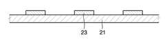
11, 21 : 제1기판13, 23 : 발광 소자11, 21:
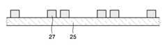
15, 25 : 제2기판18, 28 : 실링재15, 25:
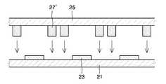
27 : 실링재 형성용 조성물27' : 열처리된 실링재 형성용 조성물27: Composition for forming sealing material 27 ': Composition for forming heat-treated sealing material
29 : 전자기파29: electromagnetic waves
본 발명은 글래스 프릿, 실링재 형성용 조성물, 발광 장치 및 발광 장치의 제조 방법에 관한 것으로서, 보다 상세하기로는, V+4 이온을 포함한 글래스 프릿, V+5 이온 및 필러를 포함한 글래스 프릿, 상기 글래스 프릿을 포함한 실링재 형성용 조성물, 상기 실링재 형성용 조성물을 이용하여 형성한 실링재를 구비한 발광 장치 및 상기 발광 장치의 제조 방법에 관한 것이다. 상기 발광 장치의 실링재는 도포법 및 전자기파 조사에 의하여 간단히 형성될 수 있어, 제조 단가가 낮으며, 실링재 형성시 발광 소자의 열화도 실질적으로 방지된다. 또한, 실링재의 실링 특성도 우수하여, 고수명을 갖는 발광 장치를 얻을 수 있다.The present invention relates to a glass frit, a composition for forming a sealing material, a light emitting device and a manufacturing method of a light emitting device, and more specifically, a glass frit containing V+4 ions, a glass frit containing V+5 ions and a filler, the glass A light emitting device comprising a composition for forming a sealing material including a frit, a sealing material formed using the composition for forming a sealing material, and a method for manufacturing the light emitting device. Since the sealing material of the light emitting device can be simply formed by the coating method and the electromagnetic wave irradiation, the manufacturing cost is low, and the deterioration of the light emitting device is substantially prevented when the sealing material is formed. Moreover, the sealing characteristic of a sealing material is also excellent, and the light emitting device which has a long lifetime can be obtained.
유기 발광 소자, 전자 방출 소자, 디스플레이 패널 등의 전자 소자는 수분 및/또는 산소의 침투에 의하여 열화되는 특성을 갖고 있다. 따라서, 상기 전자 소자의 안정적인 구동과 수명의 확보를 위하여 봉지 구조가 요구된다.Electronic devices such as organic light emitting devices, electron emitting devices, and display panels have properties that deteriorate due to penetration of moisture and / or oxygen. Therefore, an encapsulation structure is required in order to ensure stable driving and lifespan of the electronic device.
종래에는 금속 캔이나 글래스를 홈을 가지도록 캡 형태로 가공하여 그 홈에 수분 흡수를 위한 건습제를 파우더 형태로 탑재하거나 필름 형태로 제조하여 양면 테이프를 이용하여 접착하는 방법을 이용하였다.Conventionally, a metal can or glass is processed in a cap shape to have a groove, and a drying or drying agent for water absorption is mounted in a powder form or manufactured in a film form to adhere to the double-sided tape.
일본 특허공개 공보 평 9-148066호는 유기 화합물로 된 유기 발광층이 서로 대향하는 한 쌍의 전극간에 놓인 구조를 갖는 적층체와 이러한 적층체를 외기와 차단하는 기밀성 용기와 기밀성 용기 내에 배치된 알칼리 금속 산화물, 알칼리 금속 산화물과 같은 건조수단을 갖는 유기 전계 발광 표시 소자를 개시하고 있다. 그런데 이러한 유기 전계 발광 소자는 그 기밀성 용기의 형상으로 인하여 표시 장치 전체의 두께가 두꺼워진다. 또한 건조수단이 수분을 흡착한 후 고체 상태를 유지한다고 하더라도 불투명하여 전면발광에 적용할 수는 없다.Japanese Patent Laid-Open No. 9-148066 discloses a laminate having a structure in which an organic light emitting layer made of an organic compound is placed between a pair of electrodes facing each other, and an alkali metal disposed in an airtight container and an airtight container that shield the laminate from outside air. An organic electroluminescent display device having drying means such as an oxide and an alkali metal oxide is disclosed. However, due to the shape of the hermetic container, the organic electroluminescent device has a thick thickness of the entire display device. In addition, even if the drying means retains a solid state after adsorbing moisture, the drying means is not opaque and cannot be applied to front emission.
미국 특허 제6,226,890호는 0.1 내지 200㎛의 입자 크기를 갖는 고체 입자를 포함하는 흡습제 및 바인더를 이용하여 형성된 흡습층을 채용한 유기 전계 발광 소자를 개시하고 있다.U. S. Patent No. 6,226, 890 discloses an organic electroluminescent device employing a hygroscopic layer formed using a hygroscopic agent and a binder comprising solid particles having a particle size of 0.1 to 200 mu m.
그러나, 이와 같은 종래의 봉지 방법으로는 만족할 만한 수준의 수명 특성을 갖는 유기 발광 장치를 얻을 수 없는 바, 이의 개선이 필요하다.However, such an organic encapsulation method cannot obtain an organic light emitting device having satisfactory lifespan characteristics, and thus an improvement thereof is required.
본 발명이 이루고자 하는 기술적 과제는 밀봉 특성이 우수한 실링재를 구비하여 고수명을 갖는 발광 장치를 제공하는 것을 목적으로 한다. 아울러, 상기 발광 장치를 제공할 수 있는 글래스 프릿, 실링재 형성용 조성물 및 상기 발광 장치의 제조 방법도 제공하는 것을 목적으로 한다.SUMMARY OF THE INVENTION An object of the present invention is to provide a light emitting device having a high lifetime by providing a sealing material excellent in sealing properties. In addition, an object of the present invention is to provide a glass frit, a sealing material forming composition, and a manufacturing method of the light emitting device, which can provide the light emitting device.
상기 본 발명의 기술적 과제를 이루기 위하여, 본 발명은, V+4 이온을 포함한 글래스 프릿을 제공한다.In order to achieve the above technical problem, the present invention provides a glass frit containing V+ 4 ions.
본 발명의 다른 기술적 과제를 이루기 위하여, 본 발명은 V+4 이온을 포함한 글래스 프릿을 포함한 실링재 형성용 조성물을 제공한다. 상기 실링재 형성용 조성물은 지르코늄-텅스텐-포스페이트계 필러를 더 포함할 수 있다.In order to achieve the other technical problem of the present invention, the present invention provides a composition for forming a sealing material comprising a glass frit containing V+ 4 ions. The sealing material forming composition may further include a zirconium-tungsten-phosphate filler.
본 발명의 또 다른 기술적 과제를 이루기 위하여, 본 발명은 V+5 이온을 포함한 글래스 프릿 및 지르코늄-텅스텐-포스페이트계 필러를 포함한 실링재 형성용 조성물을 제공한다.In order to achieve another technical problem of the present invention, the present invention provides a composition for forming a sealing material comprising a glass frit and a zirconium-tungsten-phosphate filler containing V+5 ions.
본 발명의 또 다른 기술적 과제를 이루기 위하여, 본 발명은, 제1기판과, 제2기판과, 상기 제1기판과 상기 제2기판 사이에 구비된 발광 소자 및 상기 제1기판과 상기 제2기판을 접착시키며, 상기 발광 소자를 밀봉시키는 실링재를 구비한 발광 장치로서, 상기 실링재가 V+4 이온을 포함한 발광 장치를 제공한다.According to another aspect of the present invention, there is provided a light emitting device provided between a first substrate, a second substrate, the first substrate, and the second substrate, and the first substrate and the second substrate. A light-emitting device having a sealing material to seal the light-emitting element, wherein the sealing material contains V+4 ions.
상기 발광 장치의 실링재는 200nm 내지 10,000nm 범위의 전자기파를 방출할 수 있는 전자기파 소스를 조사하여 형성된 것일 수 있다.The sealing material of the light emitting device may be formed by irradiating an electromagnetic wave source capable of emitting electromagnetic waves in the range of 200 nm to 10,000 nm.
본 발명의 또 다른 기술적 과제를 이루기 위하여, 본 발명은, 발광 소자가 구비된 제1기판을 준비하는 단계, 전술한 바와 같은 실링재 형성용 조성물을 준비하는 단계, 상기 실링재 형성용 조성물을 제2기판의 실링재 형성 영역에 제공하는 단계, 상기 실링재 형성용 조성물이 도포된 제2기판을 열처리하는 단계, 상기 열처 리된 실링재 형성용 조성물 및 상기 발광 소자가 상기 제1기판과 상기 제2기판 사이에 구비되도록, 상기 제1기판과 상기 제2기판을 합착시키는 단계 및 열처리된 실링재 형성용 조성물에 전자기파 소스를 조사하여 실링재를 형성하는 단계를 포함하는 발광 장치의 제조 방법을 제공한다.According to another aspect of the present invention, there is provided a method of preparing a first substrate having a light emitting device, preparing a composition for forming a sealing material as described above, and forming the composition for forming a sealing material on a second substrate. Providing a sealing material forming region of the sealing material, heat treating a second substrate coated with the sealing material forming composition, and the thermally treated sealing material forming composition and the light emitting device are provided between the first substrate and the second substrate. And bonding the first substrate and the second substrate and irradiating an electromagnetic wave source to the heat-treated composition for forming a sealing material to form a sealing material.
전술한 바와 같은 본 발명을 따르는 글래스 프릿, 실링재 형성용 조성물 및 발광 장치의 제조 방법을 이용하면, 제조 단가가 낮으며, 실링 특성이 우수하고, 실링재 형성시 발광 소자의 열화가 방지되어, 장수명을 갖는 발광 장치를 얻을 수 있다.When the glass frit, the sealing composition forming composition, and the light emitting device manufacturing method according to the present invention as described above are used, the manufacturing cost is low, the sealing properties are excellent, and the deterioration of the light emitting device when forming the sealing material is prevented, resulting in long life. The light emitting device can be obtained.
이하, 본 발명을 상세히 설명한다.Hereinafter, the present invention will be described in detail.
본 발명을 따르는 글래스 프릿은 1종 이상의 이온을 포함한 산화물로서, V+4 이온을 포함한다. V+4 이온은 다양한 파장의 전자기파(electro-magnetic wave)를 흡수할 수 있는 바, V+4 이온을 포함한 글래스 프릿은 전자기파의 조사에 의하여 연화될 수 있다. 예를 들어, V+4 이온은 810nm의 레이저광을 흡수할 수 있다.Glass frit according to the present invention is an oxide containing at least one ion, and includes V+4 ions. V+4 ions can absorb electromagnetic waves of various wavelengths, glass frit containing V+4 ions can be softened by the irradiation of electromagnetic waves. For example, V+4 ions can absorb 810 nm laser light.
상기 글래스 프릿은 V+4 이온 외에도, 각종 이온을 더 포함할 수 있다. 예를 들면, V+5 이온, Ba+2 이온, Zn+2 이온, Te+4 이온, Fe+3 이온, Cu+2 이온, Nd+2 이온, K+1 이온, Sb+3 이온, P+5 이온, Ti+2 이온, Al+3 이온, B+3 이온, W+6 이온, Sn+2 이온, Bi+3 이온, Ca+2 이온, Si+4 이온, Zr+4 이온 및 Mg+2 이온으로 이루어진 군으로부터 선택된 하나 이상의 이온을 더 포함할 수 있으나, 이에 한정되는 것은 아니다.The glass frit may further include various ions in addition to V+4 ions. For example, V+5 ions, Ba+2 ions, Zn+2 ions, Te+4 ions, Fe+3 ions, Cu+2 ions, Nd+2 ions, K+1 ions, Sb+3 ions, P+5 ions, Ti+2 ions, Al+3 ions, B+3 ions, W+6 ions, Sn+2 ions, Bi+3 ions, Ca+2 ions, Si+4 ions, Zr+4 ions and Mg It may further include one or more ions selected from the group consisting of+2 ions, but is not limited thereto.
보다 구체적으로, 상기 글래스 프릿은 V+5 이온, Ba+2 이온, Zn+2 이온 및 Te+4 이온을 더 포함할 수 있다. 또는, 상기 글래스 프릿은 Ba+2 이온, Zn+2 이온 및 Te+4 이온을 더 포함할 수 있다.More specifically, the glass frit may further include V+5 ions, Ba+2 ions, Zn+2 ions, and Te+4 ions. Alternatively, the glass frit may further include Ba+2 ions, Zn+2 ions, and Te+4 ions.
상기 글래스 프릿에 포함된 이온들 중 일부는 글래스 프릿 중 V+5 이온을 V+4 이온으로 환원시키기 위한 환원제로부터 유래된 이온일 수 있다. 예를 들면, Al+3 이온, Sn2+ 이온, Mg+2 이온, Cu+2 이온, Zn+2 이온 등은, 본 발명을 따르는 글래스 프릿 중 V+5 이온을 V+4 이온으로 환원시키기 위하여, 글래스 프릿 제조시 첨가된 환원제인 Al, Sn, Mg, Cu, Zn 등으로부터 유래된 것일 수 있다. 또한, 본 발명을 따르는 글래스 프릿 중, V+5 이온을 V+4 이온으로 환원시키는 환원제로서 C(carbon)을 이용할 수 있다. 상기 환원제로서 C를 이용할 경우, 이는 글래스 프릿에 소량의 유기물로서 잔류할 수 있다.Some of the ions included in the glass frit may be ions derived from a reducing agent for reducing V+5 ions in the glass frit to V+4 ions. For example, Al+3 ions, Sn+2 ion, Mg ion+2, Cu+2 ion, Zn+2 ion and the like, to reduce the present invention that follows the glass frit of V+5 to V+4 ion ion In order to, the glass frit may be derived from Al, Sn, Mg, Cu, Zn, and the like, which are added during the preparation of the glass frit. In the glass frit according to the present invention, C (carbon) may be used as a reducing agent for reducing V+5 ions to V+4 ions. When C is used as the reducing agent, it may remain in the glass frit as a small amount of organic matter.
상기 글래스 프릿은 전자기파를 효과적으로 흡수할 수 있도록, 0.1㎛ 내지 30㎛, 바람직하게는, 0.5㎛ 내지 15㎛의 평균 입경을 가질 수 있다. 한편, 상기 글래스 프릿의 최대 입경은 1㎛ 내지 150㎛, 바람직하게는 3㎛ 내지 30㎛의 최대 입자 크기를 가질 수 있다.The glass frit may have an average particle diameter of 0.1 μm to 30 μm, preferably 0.5 μm to 15 μm, to effectively absorb electromagnetic waves. Meanwhile, the maximum particle diameter of the glass frit may have a maximum particle size of 1 μm to 150 μm, preferably 3 μm to 30 μm.
전술한 바와 같은 V+4 이온을 포함한 글래스 프릿을 제조하는 방법의 일 구현예는 다음과 같다.One embodiment of the method for manufacturing the glass frit including the V+4 ions as described above is as follows.
먼저, V2O5를 포함한 각종 산화물 및 V+5 이온을 V+4 이온으로 환원시키는 환원제를 혼합한다.First, various oxides including V2 O5 and a reducing agent for reducing V+5 ions to V+4 ions are mixed.
V2O5 외에 사용가능한 각종 산화물의 예로는 BaO, ZnO, TeO2, Fe2O3, CuO, NdO, K2O, Sb2O3, P2O5, TiO, Al2O3, B2O3, WO6, SnO, Bi2O3, CaO, SiO2, ZrO2 등이 있으나, 이에 한정되는 것은 아니다. 한편, 상기 환원제의 예로는 Al, Sn, Mg, Cu, Zn, 탄소 등이 있으나, 이에 한정되는 것은 아니다.Examples of various oxides that can be used in addition to V2 O5 include BaO, ZnO, TeO2 , Fe2 O3 , CuO, NdO, K2 O, Sb2 O3 , P2 O5 , TiO, Al2 O3 , B2 O3 , WO6 , SnO, Bi2 O3 , CaO, SiO2 , ZrO2 and the like, but is not limited thereto. Meanwhile, examples of the reducing agent include Al, Sn, Mg, Cu, Zn, carbon, and the like, but are not limited thereto.
그리고 나서, 이를 도가니에 넣고, 열처리한다. 열처리 온도 및 열처리 온도는 용융시키고자 하는 산화물 및 환원제의 종류 및 양에 따라 상이하나, 대략적으로 600℃ 내지 1200℃의 온도 범위 및 10분 내지 240분의 온도 범위에서 선택될 수 있다. 이로부터 얻은 융해물을 냉각시켜 글래스를 얻은 다음, 이를 분쇄하여 V+4 이온을 포함한 글래스 프릿을 얻을 수 있다.It is then placed in a crucible and heat treated. The heat treatment temperature and the heat treatment temperature vary depending on the type and amount of the oxide and the reducing agent to be melted, but may be selected from a temperature range of approximately 600 ° C. to 1200 ° C. and a temperature range of 10 minutes to 240 minutes. The resulting melt can be cooled to obtain glass and then ground to obtain a glass frit containing V+4 ions.
전술한 바와 같은 V+4 이온을 포함한 글래스 프릿은 발광 장치의 실링재 형성용 조성물에 포함될 수 있다. 상기 V+4 이온을 포함한 글래스 프릿에 대한 상세한 설명은 전술한 바를 참조한다.The glass frit including the V+4 ions as described above may be included in the composition for forming a sealing material of the light emitting device. For a detailed description of the glass frit containing the V+4 ions refer to the foregoing.
상기 실링재 형성용 조성물은, V+4 이온을 포함한 글래스 프릿을 포함하는 바, 200nm 내지 10,000nm 파장 범위의 전자기파를 흡수할 수 있다. 따라서, 상기 실링재 형성용 조성물은 전술한 바와 같은 파장 범위를 갖는 전자기파 조사에 의하여 효과적으로 연화될 수 있다.The sealing material forming composition may include a glass frit including V+4 ions, and may absorb electromagnetic waves in a wavelength range of 200 nm to 10,000 nm. Therefore, the composition for forming the sealing material can be effectively softened by the electromagnetic wave irradiation having a wavelength range as described above.
상기 실링재 형성용 조성물은 전자기파 조사에 의하여 연화되면서 그 체적이 팽창될 수 있다. 이 경우, 우수한 밀봉 특성을 갖는 실링재를 얻기 곤란할 수 있다. 따라서, 상기 실링재 형성용 조성물은 열팽창 계수를 낮출 수 있는 필러를 더 포함할 수 있다.The sealing material forming composition may be expanded in volume while being softened by electromagnetic wave irradiation. In this case, it may be difficult to obtain a sealing material having excellent sealing properties. Therefore, the sealing material forming composition may further include a filler capable of lowering the coefficient of thermal expansion.
상기 필러의 구체예로는 지르코늄-텅스텐-포스페이트계 필러, 지르코늄-포스페이트계 필러(예를 들면, 인산 지르코늄), 지르코늄계 필러(예를 들면, 지르코늄), 유크립타이트계 필러(예를 들면, β-유크립타이트), 코디어라이트계 필러, 알루미나, 실리카, 규산 아연, 티탄산 알루미늄 등을 들 수 있으나, 이에 한정되는 것은 아니다. 이 중, 2 이상의 조합을 사용할 수 있음은 물론이다.Specific examples of the filler include zirconium-tungsten-phosphate fillers, zirconium-phosphate fillers (e.g. zirconium phosphate), zirconium fillers (e.g. zirconium), eutectic fillers (e.g. β-eucryptite), cordierite-based fillers, alumina, silica, zinc silicate, aluminum titanate, and the like, but are not limited thereto. Of course, two or more combinations can be used.
보다 구체적으로, 상기 지르코늄-텅스텐-포스페이트계 필러는 예를 들면, (Zr2(WO4)(PO4)2)일 수 있으나, 이에 한정되는 것은 아니다.More specifically, the zirconium-tungsten-phosphate filler may be, for example, (Zr2 (WO4 ) (PO4 )2 ), but is not limited thereto.
전술한 바와 같은 실링재 형성용 조성물에 포함될 수 있는 필러는 전자기파 조사에 의하여 효과적으로 연화되는 것이 바람직하다. 이를 고려하여, 상기 필러의 평균 입경은 0.1㎛ 내지 30㎛, 바람직하게는 0.5㎛ 내지 15㎛일 수 있다. 한편, 상기 필러의 최대 입경은 1㎛ 내지 150㎛, 바람직하게는 3㎛ 내지 30㎛일 수 있다.The filler that may be included in the composition for forming a sealing material as described above is preferably softened by electromagnetic wave irradiation. In consideration of this, the average particle diameter of the filler may be 0.1㎛ to 30㎛, preferably 0.5㎛ to 15㎛. On the other hand, the maximum particle diameter of the filler may be 1㎛ to 150㎛, preferably 3
전술한 바와 같은 실링재 형성용 조성물의 열팽창 계수는 25 x 10-7/℃ 내지 95 x 10-7/℃, 바람직하게는, 35 x 10-7/℃ 내지 65 x 10-7/℃가 될 수 있다. 이로써, 본 발명을 따르는 발광 장치의 실링재 형성시 전자기파 조사에 의한 체적 변화에 따른 기판 간 부정합을 방지할 수 있다.The coefficient of thermal expansion of the composition for forming a sealing material as described above may be 25 x 10-7 / ℃ to 95 x 10-7 / ℃, preferably, 35 x 10-7 / ℃ to 65 x 10-7 / ℃ have. As a result, when the sealing material of the light emitting device according to the present invention is formed, misalignment between substrates due to volume changes due to electromagnetic wave irradiation can be prevented.
전술한 바와 같은 필러의 함량은 전술한 바와 같은 열팽창 계수 범위를 얻을 수 있으면서도, 글래스 프릿의 함량이 지나치게 감소되지 않는 범위 내에서 선택될 수 있다. 예를 들면, 상기 필러의 함량은 글래스 프릿의 함량 및 필러의 함량의 합 100중량부 당 5중량부 내지 80중량부, 바람직하게는 20중량부 내지 60중량부 범위에서 선택될 수 있다.The content of the filler as described above can be selected within the range in which the content of the glass frit is not excessively reduced while the thermal expansion coefficient range as described above can be obtained. For example, the content of the filler may be selected from 5 parts by weight to 80 parts by weight, preferably 20 parts by weight to 60 parts by weight, per 100 parts by weight of the content of the glass frit and the content of the filler.
한편, 상기 실링재 형성용 조성물은 적절한 인쇄성, 점도, 흐름성 등을 얻기 위하여 비이클을 더 포함할 수 있다. 상기 비이클은 실링재 형성용 조성물을 기판에 제공한 다음, 열처리 시 분해될 수 있도록 유기물일 수 있다.On the other hand, the sealing material forming composition may further comprise a vehicle to obtain a suitable printability, viscosity, flowability and the like. The vehicle may be an organic material to provide a composition for forming a sealing material to a substrate and then decompose during heat treatment.
예를 들면, 상기 비이클은 수지 및 용매를 포함할 수 있다. 상기 수지는, 예를 들면, 아크릴계 수지, 메타크릴계 수지, 비닐계 수지, 에폭시계 수지, 우레탄계 수지 및 셀롤로오즈계 수지로 이루어진 군으로부터 선택된 하나 이상의 수지일 수 있으나, 이에 한정되는 것은 아니다. 상기 용매는, 테르피놀(terpinol), 디히드로테르피놀(dihydro terpinol), 부틸카르비톨아세티이트(butylcarbitolacetate), 부틸카르비톨(butyl carbitol) 및 2,2,4-트리메틸-1,3-펜탄디올모노부티레이 트(2,2,4-trimethyl- 1,3-pentadiol monobutyrate)으로 이루어진 군으로부터 선택된 하나 이상일 수 있으나, 이에 한정되는 것은 아니다.For example, the vehicle may include a resin and a solvent. The resin may be, for example, one or more resins selected from the group consisting of acrylic resins, methacryl resins, vinyl resins, epoxy resins, urethane resins and cellulose resins, but is not limited thereto. The solvent includes terpinol, dihydro terpinol, butylcarbitolacetate, butyl carbitol and 2,2,4-trimethyl-1,3-pentane Diol monobutyrate (2,2,4-trimethyl-1,3-pentadiol monobutyrate) may be one or more selected from the group consisting of, but is not limited thereto.
보다 구체적으로서, 상기 아크릴계 수지의 예로서, 부틸아그릴레이트, 에틸헥실아크릴레이트 등이 있고, 상기 메타크릴계 수지의 예로서, 프로필렌글리콜메타크릴레이트,테트라하이드로퍼프리 메타크릴레이트 등이 있고, 상기 비닐계 수지의 예로서 비닐아세테이트,N-비닐피롤리돈 등이 있고, 에폭시계 수지의 예로서, 싸이클로알리파틱 에폭사이드, 에폭시 아크릴레이트 등이 있고, 우레탄계 수지의 예로서, 우레탄 아크릴레이트 등이 있고, 셀룰로오즈계 수지의 예로서, 에틸셀룰로오즈, 셀룰로오즈나이트레이트 등이 있으나 이에 한정되는 것은 아니다.More specifically, examples of the acrylic resin include butyl acrylate, ethylhexyl acrylate, and the like. Examples of the methacryl resin include propylene glycol methacrylate, tetrahydrofurfree methacrylate, and the like. Examples of the vinyl resins include vinyl acetate, N-vinylpyrrolidone, and the like. Examples of the epoxy resins include cycloaliphatic epoxides and epoxy acrylates. Examples of the urethane resins include urethane acrylates and the like. Examples of the cellulose-based resin include, but are not limited to, ethyl cellulose, cellulose nitrate, and the like.
상기 비이클의 함량은 실링재 형성용 조성물의 인쇄성, 점도, 흐름성 등을 고려하여 선택될 수 있는데, 예를 들면, 상기 실링재 형성용 조성물 100중량부 당 10중량부 내지 60중량부, 바람직하게는, 20중량부 내지 50중량부의 범위 내에서 선택될 수 있다.The content of the vehicle may be selected in consideration of printability, viscosity, flowability, etc. of the composition for forming the sealing material, for example, 10 parts by weight to 60 parts by weight, preferably 100 parts by weight of the composition for forming the sealing material. It can be selected within the range of 20 parts by weight to 50 parts by weight.
한편, 본 발명을 따르는 실링재 형성용 조성물은 V+5 이온을 포함한 글래스 프릿 및 필러를 포함하되, 상기 필러를 지르코늄-텅스텐-포스페이트계 필러일 수 있다.Meanwhile, the composition for forming a sealing material according to the present invention includes a glass frit and a filler including V+5 ions, and the filler may be a zirconium-tungsten-phosphate filler.
본 명세서에 있어서, "V+5 이온을 포함한 글래스 프릿"은 V+4 이온을 포함하지 않은 글래스 프릿을 의미한다. 후술하는 바와 같이 본 발명을 따르는 발광 장치의 실링재는 반드시 V+4 이온을 포함하나, 상기 V+4 이온은 다양한 방법으로 실링 재에 포함될 수 있다. 예를 들면, 앞서 언급한 바와 같이 글래스 프릿 자체가 V+4 이온을 포함할 수도 있으나, V+4 이온을 포함하지 않은 글래스 프릿을 이용하더라도, 환원제를 이용하거나, 환원 분위기 하에서 열처리하여 V+5 이온을 V+4 이온으로 환원시킬 수 있다. 즉, 상기 V+5 이온을 포함한 글래스 프릿 및 필러를 포함한 실링재 형성용 조성물은 글래스 프릿 자체가 V+4 이온을 포함하지는 않지만, 환원제를 이용하거나, 환원 분위기 하에서 열처리 됨으로서, V+4 이온을 포함할 수 있다.In the present specification, "glass frit containing V+5 ions" means glass frit not containing V+4 ions. Sealing materials must include, V+4 ion, the V+4 ion of the light-emitting device according to an embodiment of the present invention as described below can be included in the sealing material in a variety of ways. For example, as mentioned above, the glass frit itself may include V+4 ions, but even if glass frit containing no V+4 ions is used, V+5 may be used by using a reducing agent or by heat treatment in a reducing atmosphere. Ions can be reduced to V+4 ions. That is, the V composition for forming a sealing material including a glass frit and filler including+5 ions the glass frit does not include V+4 ion itself, by being heat-treated under using a reducing agent, or a reducing atmosphere, include V+4 ion can do.
상기 실링재 형성용 조성물 중 V+5 이온을 포함한 글래스 프릿은 Ba+2 이온, Zn+2 이온, Te+4 이온, Fe+3 이온, Cu+2 이온, Nd+2 이온, K+1 이온, Sb+3 이온, P+5 이온, Ti+2 이온, Al+3 이온, B+3 이온, W+6 이온, Sn+2 이온 및 Bi+3 이온, Ca+2 이온, Si+4 이온, Zr+4 이온 및 Mg+2 이온으로 이루어진 군으로부터 선택된 하나 이상의 이온을 더 포함할 수 있으나, 이에 한정되는 것은 아니다.Glass frit containing V+5 ions in the composition for forming the sealing material is Ba+2 ions, Zn+2 ions, Te+4 ions, Fe+3 ions, Cu+2 ions, Nd+2 ions, K+1 ions, Sb+3 ions, P+5 ions, Ti+2 ions, Al+3 ions, B+3 ions, W+6 ions, Sn+2 ions and Bi+3 ions, Ca+2 ions, Si+4 ions, It may further include one or more ions selected from the group consisting of Zr+4 ions and Mg+2 ions, but is not limited thereto.
보다 구체적으로, 상기 V+5 이온을 포함한 글래스 프릿은 Ba+2 이온, Zn+2 이온 및 Te+4 이온을 더 포함할 수 있다.More specifically, the glass frit including the V+5 ions may further include Ba+2 ions, Zn+2 ions, and Te+4 ions.
상기 글래스 프릿은 전자기파를 효과적으로 흡수할 수 있도록, 0.1㎛ 내지 30㎛, 바람직하게는, 0.5㎛ 내지 15㎛의 평균 입경을 가질 수 있다. 한편, 상기 글래스 프릿의 최대 입경은 1㎛ 내지 150㎛, 바람직하게는 3㎛ 내지 30㎛일 수 있다.The glass frit may have an average particle diameter of 0.1 μm to 30 μm, preferably 0.5 μm to 15 μm, to effectively absorb electromagnetic waves. Meanwhile, the maximum particle diameter of the glass frit may be 1 μm to 150 μm, preferably 3 μm to 30 μm.
한편, 상기 실링재 형성용 조성물에 포함된 지르코늄-텅스텐-포스페이트계 필러는 (Zr2(WO4)(PO4)2)일 수 있으나, 이에 한정되는 것은 아니다.Meanwhile, the zirconium-tungsten-phosphate filler included in the sealing material forming composition may be (Zr2 (WO4 ) (PO4 )2 ), but is not limited thereto.
상기 실링재 형성용 조성물은 지르코늄-포스페이트계 필러(예를 들면, 인산 지르코늄), 지르코늄계 필러(예를 들면, 지르코늄), 유크립타이트계 필러(예를 들면, β-유크립타이트), 코디어라이트계 필러, 알루미나, 실리카, 규산 아연 및 티탄산 알루미늄으로 이루어진 군으로부터 선택된 필러를 더 포함할 수 있으나, 이에 한정되는 것은 아니다.The sealing material forming composition may be a zirconium-phosphate filler (for example, zirconium phosphate), a zirconium filler (for example zirconium), a eu cryptite filler (for example β-eucryptite), cordier The light filler may further include a filler selected from the group consisting of alumina, silica, silica, zinc silicate, and aluminum titanate, but is not limited thereto.
전술한 바와 같은 실링재 형성용 조성물에 포함될 수 있는 필러는 전자기파 조사에 의하여 효과적으로 연화되는 것이 바람직하다. 이를 고려하여, 상기 필러의 평균 입경은 0.1㎛ 내지 30㎛, 바람직하게는 0.5㎛ 내지 15㎛일 수 있다. 한편, 상기 필러의 최대 입경은 1㎛ 내지 150㎛, 바람직하게는 3㎛ 내지 60㎛일 수 있다.The filler that may be included in the composition for forming a sealing material as described above is preferably softened by electromagnetic wave irradiation. In consideration of this, the average particle diameter of the filler may be 0.1㎛ to 30㎛, preferably 0.5㎛ to 15㎛. On the other hand, the maximum particle diameter of the filler may be 1㎛ to 150㎛, preferably 3㎛ to 60㎛.
전술한 바와 같은 실링재 형성용 조성물의 열팽창 계수는 25 x 10-7/℃ 내지 95 x 10-7/℃, 바람직하게는, 35 x 10-7/℃ 내지 65 x 10-7/℃가 될 수 있다. 이로써, 본 발명을 따르는 발광 장치의 실링재 형성시 전자기파 조사에 의한 체적 변화에 따른 기판 간 부정합을 방지할 수 있다.The coefficient of thermal expansion of the composition for forming a sealing material as described above may be 25 x 10-7 / ℃ to 95 x 10-7 / ℃, preferably, 35 x 10-7 / ℃ to 65 x 10-7 / ℃ have. As a result, when the sealing material of the light emitting device according to the present invention is formed, misalignment between substrates due to volume changes due to electromagnetic wave irradiation can be prevented.
전술한 바와 같은 필러의 함량은 전술한 바와 같은 열팽창 계수 범위를 얻을 수 있으면서도, 글래스 프릿의 함량이 지나치게 감소되지 않는 범위 내에서 선택될 수 있다. 예를 들면, 상기 필러의 함량은 글래스 프릿의 함량 및 필러의 함량 합 100중량부 당 5중량부 내지 80중량부, 바람직하게는 20중량부 내지 60중량부 범위에서 선택될 수 있다.The content of the filler as described above can be selected within the range in which the content of the glass frit is not excessively reduced while the thermal expansion coefficient range as described above can be obtained. For example, the content of the filler may be selected from 5 parts by weight to 80 parts by weight, preferably 20 parts by weight to 60 parts by weight, per 100 parts by weight of the content of the glass frit and the content of the filler.
한편, 상기 V+5 이온을 포함한 글래스 프릿 및 필러를 포함한 실링재 헝성용 조성물은 환원제를 더 포함할 수 있다. 상기 환원제는 V+5 이온을 V+4 이온으로 환원시키는 역할을 한다. 예를 들면, 본 발명을 따르는 실링재 형성용 조성물은 기판에 도포된 다음, 전자기파 소스로 조사되기 전 열처리 과정을 거치는데, 이 때, 실링재 형성용 조성물에 포함된 환원제에 의하여, 글래스 프릿 중 V+5 이온은 V+4 이온으로 환원될 수 있다.On the other hand, the sealing material for the composition for forming a sealing material comprising a glass frit and filler containing the V+5 ion may further comprise a reducing agent. The reducing agent serves to reduce V+5 ions to V+4 ions. For example, the sealing material forming composition according to the present invention is applied to a substrate, and then subjected to a heat treatment process before being irradiated with an electromagnetic wave source, wherein, by the reducing agent included in the sealing material forming composition, V+ of the glass frit5 ions can be reduced to V+4 ions.
상기 환원제의 예로는 Al, Sn, Mg, Cu, Zn, 탄소 등이 있으나, 이에 한정되는 것은 아니다.Examples of the reducing agent include Al, Sn, Mg, Cu, Zn, carbon and the like, but is not limited thereto.
상기 환원제의 함량은 글래스 프릿의 함량, 실링재 형성용 조성물의 열처리 온도 및 시간에 의하여 상이할 것이나, 대략적으로, 글래스 프릿 100중량부 당 0.01중량부 내지 20중량부, 바람직하게는 0.1중량부 내지 2중량부의 범위 내에서 선택될 수 있다.The content of the reducing agent will be different depending on the content of the glass frit, the heat treatment temperature and time of the composition for forming the sealing material, but approximately, 0.01 to 20 parts by weight, preferably 0.1 to 2 parts by weight per 100 parts by weight of glass frit. It may be selected within the range of parts by weight.
한편, 상기 실링재 형성용 조성물은 적절한 인쇄성, 점도, 흐름성 등을 얻기 위하여 비이클을 더 포함할 수 있다. 상기 비이클은 실링재 형성용 조성물을 기판에 제공한 다음, 열처리 시 분해될 수 있도록 유기물일 수 있다.On the other hand, the sealing material forming composition may further comprise a vehicle to obtain a suitable printability, viscosity, flowability and the like. The vehicle may be an organic material to provide a composition for forming a sealing material to a substrate and then decompose during heat treatment.
예를 들면, 상기 비이클은 수지 및 용매를 포함할 수 있다. 상기 수지는,예를 들면, 아크릴계 수지, 메타크릴계 수지, 비닐계 수지, 에폭시계 수지, 우레탄계 수지 및 셀롤로오즈계 수지로 이루어진 군으로부터 선택된 하나 이상일 수 있으나, 이에 한정되는 것은 아니다. 한편, 상기 용매는 테르피놀(terpinol), 디히드로테르피놀(dihydroterpinol), 부틸카르비톨아세티이트(butylcarbitolacetate), 부틸카르비톨(butylcarbitol) 및 2,2,4-트리메틸-1,3-펜탄디올모노부티레이트(2,2,4-trimethyl- 1,3-pentadiol monobutyrate)로 이루어진 군으로부터 선택된 하나 이상일 수 있으나, 이에 한정되는 것은 아니다.For example, the vehicle may include a resin and a solvent. The resin may be, for example, at least one selected from the group consisting of acrylic resins, methacryl resins, vinyl resins, epoxy resins, urethane resins, and cellulose resins, but is not limited thereto. On the other hand, the solvent is terpinol (terpinol), dihydroterpinol (dihydroterpinol), butylcarbitolacetate (butylcarbitolacetate), butylcarbitol (butylcarbitol) and 2,2,4-trimethyl-1,3-pentanediol Monobutyrate (2,2,4-trimethyl-1,3-pentadiol monobutyrate) may be one or more selected from the group consisting of, but is not limited thereto.
한편, 상기 비이클 중 일부 이상은 전술한 바와 같은 V+5 이온을 V+4 이온으로 환원시키는 환원제로의 역할을 수행할 수도 있다.Meanwhile, at least some of the vehicle may serve as a reducing agent for reducing V+5 ions to V+4 ions as described above.
보다 구체적으로서, 상기 아크릴계 수지의 예로서, 부틸아그릴레이트, 에틸헥실아크릴레이트 등이 있고, 상기 메타크릴계 수지의 예로서, 프로필렌글리콜메타크릴레이트,테트라하이드로퍼프리 메타크릴레이트 등이 있고, 상기 비닐계 수지의 예로서 비닐아세테이트,N-비닐피롤리돈 등이 있고, 에폭시계 수지의 예로서, 싸이클로알리파틱 에폭사이드, 에폭시 아크릴레이트 등이 있고, 우레탄계 수지의 예로서, 우레탄 아크릴레이트 등이 있고, 셀룰로오즈계 수지의 예로서, 에틸셀룰로오즈, 셀룰로오즈나이트레이트 등이 있으나 이에 한정되는 것은 아니다.More specifically, examples of the acrylic resin include butyl acrylate, ethylhexyl acrylate, and the like. Examples of the methacryl resin include propylene glycol methacrylate, tetrahydrofurfree methacrylate, and the like. Examples of the vinyl resins include vinyl acetate, N-vinylpyrrolidone, and the like. Examples of the epoxy resins include cycloaliphatic epoxides and epoxy acrylates. Examples of the urethane resins include urethane acrylates and the like. Examples of the cellulose-based resin include, but are not limited to, ethyl cellulose, cellulose nitrate, and the like.
상기 비이클의 함량은 실링재 형성용 조성물의 인쇄성, 점도, 흐름성 등을 고려하여 선택될 수 있는데, 예를 들면, 실링재 형성용 조성물 100중량부 당 10중 량부 내지 60중량부, 바람직하게는, 20중량부 내지 50중량부의 범위 내에서 선택될 수 있다.The content of the vehicle may be selected in consideration of printability, viscosity, flowability, etc. of the composition for forming a sealing material, for example, 10 parts by weight to 60 parts by weight, preferably, per 100 parts by weight of the composition for forming a sealing material. It may be selected within the range of 20 parts by weight to 50 parts by weight.
이상, 살펴본 바와 같은 i) V+4 이온을 포함한 글래스 프릿을 포함한 실링재 형성용 조성물 및 ii) V+5 이온을 포함한 글래스 프릿을 포함한 실링재 형성용 조성물은 각종 전자 장치, 예를 들면 유기 발광 표시 장치, 전자 방출 표시 장치, 플라즈마 디스플레이 패널 등에 있어서, 발광 소자를 산소 및/또는 수분으로부터 차단하여 밀봉하는 실링재를 형성하는데 사용될 수 있다.As described above, the composition for forming a sealing material including the glass frit containing i) V+ 4 ions and the composition for forming the sealing material including the glass frit containing V+ 5 ions are described in various electronic devices, for example, an organic light emitting display device. In an electron emission display device, a plasma display panel, or the like, the light emitting device may be used to form a sealing material that seals off a light emitting element from oxygen and / or moisture.
한편, i) V+4 이온을 포함한 글래스 프릿을 포함한 실링재 형성용 조성물 중, V+4 이온을 포함한 글래스 프릿은 V+4 이온 외에도 V+5 이온을 더 포함할 수 있으므로, 필요에 따라, ii) V+5 이온을 포함한 글래스 프릿을 포함한 실링재 형성용 조성물에 추가될 수 있는 환원제를 더 포함하여, 잔존하는 V+5 이온을 추가로 환원시킬 수도 있다.On the other hand, i) of the V+4 for sealing material including a glass frit containing an ion-forming composition, the glass frit includes V+4 V+4 ion in addition to ion can further include V+5 ion, as needed, ii ) further comprises a reducing agent that can be added to the composition for forming a sealing material including a glass frit including the V+5 ion it may be reduced by adding V+5 ion remaining.
본 발명을 따르는 발광 장치는, 제1기판, 제2기판, 상기 제1기판과 상기 제2기판 사이에 구비된 발광 소자 및 상기 제1기판과 상기 제2기판을 접착시키고, 상기 발광 소자를 밀봉시키는 실링재를 포함한다. 본 발명을 따르는 발광 장치의 일 구현예를 도시한 도 1을 참조하여, 본 발명을 따르는 발광 장치를 보다 상세히 설명하기로 한다.A light emitting device according to the present invention includes a first substrate, a second substrate, a light emitting element provided between the first substrate and the second substrate, and the first substrate and the second substrate are bonded to each other, and the light emitting element is sealed. Sealing material to be included. With reference to FIG. 1, which shows an embodiment of a light emitting device according to the present invention, a light emitting device according to the present invention will be described in more detail.
도 1은 본 발명을 따르는 발광 장치의 일 구현예로서, 발광 소자가 유기 발광 소자인 유기 발광 장치의 단면도를 개략적으로 도시한 것이다.1 schematically shows a cross-sectional view of an organic light emitting device in which the light emitting device is an organic light emitting device as an embodiment of the light emitting device according to the present invention.
도 1의 발광 장치(10)는 제1기판(11) 및 제2기판(15)을 구비하고, 상기 제1기판(11) 상부에는 발광 소자(13)가 구비되어 있다. 도 1의 발광 장치(1) 중 제2기판(15)은 봉지 기판의 역할을 한다. 그리고, 상기 제1기판(11)과 제2기판(15) 사이에는, 제1기판(11)과 제2기판(15)을 서로 접착시키고, 발광 소자를 밀봉시키는 실링재(18)가 구비되어 있다. 상기 실링재(18)은 V+4 이온을 포함한다.The
상기 제1기판(11)은 각종 발광 장치에서 통상적으로 사용할 수 있는 기판이라면 특별히 한정되지 않는다. 예를 들면, 유리 기판, 금속 기판, 플라스틱재 기판 등을 사용할 수 있으나, 이에 한정되는 것은 아니다.The
상기 기판(11) 상부에는 유기 발광 소자(13)가 구비되어 있다.The organic
도 2는 상기 유기 발광 소자(13)의 일 구현예의 단면도를 개략적으로 도시한 것이다. 보다 구체적으로, 도 2는 능동(active matrix type:AM) 구동형 유기 발광 소자의 일 구현예의 단면도를 개략적으로 도시한 것이다.2 is a schematic cross-sectional view of an embodiment of the organic
기판(11)의 상면에는 기판(11)의 평활성과 불순 원소의 침투를 차단하기 위하여 버퍼층(41)이 구비되어 있다. 버퍼층(41)은 SiO2 및/또는 SiNx 등으로 형성할 수 있으나, 이에 한정되는 것은 아니다.The upper surface of the
기판(11)의 상면에 박막 트랜지스터(TFT)가 구비되어 있다. 상기 박막 트랜지스터(TFT)는 각 화소별로 하나 이상 구비될 수 있다.The thin film transistor TFT is provided on the upper surface of the
구체적으로 버퍼층(41)상에 소정 패턴의 반도체층(42)이 형성되어 있다. 반도체층(42)은 아모퍼스 실리콘 또는 폴리 실리콘과 같은 무기 반도체 물질 또는 펜타센 등과 같은 유기 반도체 물질을 포함할 수 있으며, 소스 영역, 드레인 영역 및 채널 영역을 포함한다.Specifically, the
반도체층(42)의 상부에는 SiO2, SiNx 등으로 형성되는 게이트 절연막(43)이 구비되어 있으며, 상기 게이트 절연막(43) 상부에는 게이트 전극(44)이 구비되어 있다. 게이트 전극(44)은 MoW, Al/Cu 등과 같은 물질을 포함하나, 이에 한정되는 것은 아니며, 인접층과의 밀착성, 적층되는 층의 평탄성, 전기 저항 및 가공성 등을 고려하여 다양한 재료로 이루어질 수 있다.A
게이트 전극(44)은 TFT 온/오프 신호를 인가하는 게이트 라인(미도시)과 연결되어 있다.The
게이트 전극(44)의 상부로는 층간 절연막(45)이 구비되어 있고, 층간 절연막(45) 상부로는 소스 전극(46) 및 드레인 전극(47)이 구비되어 있다. 상기 소스 전극(46) 및 드레인 전극(47)은 예를 들면, Au, Pd, Pt, Ni, Rh, Ru, Ir, Os, Al, Mo, 외에도, Al:Nd 합금, MoW 합금 등과 같은 2 종 이상의 금속으로 이루어진 합금을 사용할 수 있으며, 금속의 산화물로서는 ITO, IZO, NiO, Ag2O, In2O3-Ag2O, CuAlO2, SrCu2O2 및 Zr으로 도핑된 ZnO 등을 사용할 수 있으나, 이에 한정되는 것은 아니다. 전술한 바와 같은 금속 또는 금속 산화물 중 2 이상을 조합하여 사용할 수 있음은 물론이다.An interlayer insulating
상기 소스 전극(46) 및 드레인 전극(47)은 콘택홀을 통하여 각각 반도체층(42)의 소스 및 드레인 영역에 전기적으로 연결될 수 있다. 이와 같은 TFT 상부에는 패시베이션막(48)이 구비되어 있다.The
패시베이션막(48)은 무기물 및/또는 유기물을 포함할 수 있다. 상기 무기물의 예에는 SiO2, SiNx, SiON, Al2O3, TiO2, Ta2O5, HfO2, ZrO2, BST, PZT 등을 포함할 수 있고, 상기 유기물의 예로는 일반 범용고분자(PMMA, PS), phenol그룹을 갖는 고분자 유도체, 아크릴계 고분자, 이미드계 고분자, 아릴에테르계 고분자, 아마이드계 고분자, 불소계고분자, p-자일렌계 고분자, 비닐알콜계 고분자 및 이들의 블렌드 등을 포함할 수 있으나, 이에 한정되는 것은 아니다. 상기 패시베이션막(48)은 무기 절연막과 유기 절연막의 복합 적층체로도 형성할 수 있다.The
패시베이션막(48) 상부에는 유기 발광 소자(50)의 애노드 전극이 될 수 있는 제1전극(51)이 구비되어 있다. 상기 제1전극(51)은 예를 들면, 일함수가 높은 ITO, IZO, ZnO, 또는 In2O3 등을 이용하여 투명 전극으로 구비될 수 있다. 또는, Ag, Mg, Al, Pt, Pd, Au, Ni, Nd, Ir, Cr, Li, Ca 및 이들의 조합을 포함하는 반사막을 형성한 후, 그 위에 일함수가 높은 ITO, IZO, ZnO, 또는 In2O3 등을 형성함으로써, 반사 전극으로서 구비될 수 있는 등, 다양한 변형예가 가능하다. 상기 제1전극(51)은 TFT의 드레인 전극(47)과 전기적으로 연결되어 있다.The
상기 제1전극(51) 상부로는 화소 정의막(49)(pixel define layer)이 구비되어 있는데, 상기 화소 정의막(49)은 제1전극(51)의 일부 이상을 노출시키며 유기 층(52)이 구비될 수 있는 개구부를 갖는다. 상기 화소 정의막(49)의 개구부에는 유기층(52)이 구비되어 있으며, 그 상부로는 캐소드 전극이 되는 제2전극(53)이 구비되어 있다.The
제1전극(51)과 제2전극(53)의 사이에 개재된 유기층(52)은 제1전극(51)과 제2전극(53)의 전기적 구동에 의해 발광한다. 유기층(52)은 저분자 또는 고분자 유기물을 사용할 수 있다. 한편, 상기 유기층(52)는 정공 주입층, 정공 수송층, 전자 저지층, 발광층, 정공 저지층, 전자 수송층 및 전자 주입층으로 이루어진 군으로부터 선택된 하나 이상의 층을 필요에 따라 포함할 수 있다. 사용 가능한 저분자 유기 재료로는 구리 프탈로시아닌(CuPc: copper phthalocyanine), N,N-디(나프탈렌-1-일)-N,N'-디페닐-벤지딘 (N,N'-Di(naphthalene-1-yl)-N,N'-diphenyl-benzidine: NPB) , 트리스-8-하이드록시퀴놀린 알루미늄(tris-8-hydroxyquinoline aluminum)(Alq3) 등을 들 수 있으며, 고분자 유기 재료로는 폴리에틸렌 디히드록시티오펜 (PEDOT: poly-(2,4)-ethylene-dihydroxy thiophene)이나, 폴리아닐린(PANI: polyaniline) 등을 이용할 수 있으나, 이에 한정되지 않음은 물론이다. 상기 유기층(52)은 증착법, 레이저를 이용한 열전사 방식, 잉크젯 프린팅, 스핀 코팅법 등과 같은 다양한 방법을 이용하여 형성될 수 있다.The
상기 제2 전극(53)은 일함수가 작은 금속 즉, Ag, Mg, Al, Pt, Pd, Au, Ni, Nd, Ir, Cr, Li, Ca 등을 이용한 투명 전극 또는 반사 전극일 있다. 또는, ITO, IZO, ZnO, 또는 In2O3 등의 투명 도전물질로 보조 전극층이나 버스 전극 라인을 추 가로 형성할 수 있는 등 다양한 변형예가 가능하다.The
비록 미도시하였으나, 상기 제2전극(53) 상부로는 보호층을 추가로 형성할 수 있는데, 상기 보호층은 내열성, 내화학성, 내투습성을 제공하여, 유기층(52)에 수분 및/또는 산소가 침투하는 것을 추가로 방지하는 역할을 한다. 상기 보호층은 무기층이거나, 무기층과 유기층이 교대로 적층된 구조를 가질 수 있는 등, 다양한 변형예가 가능하다.Although not shown, a protective layer may be further formed on the
상기 보호층에 포함될 수 있는 무기층은 실리콘 질화물, 알루미늄 질화물, 지르코늄 질화물, 티타늄 질화물, 하프늄 질화물, 탄탈륨 질화물, 실리콘 산화물, 알루미늄 산화물, 티타늄 산화물, 주석산화물, 세륨 산화물 및 실리콘 산화질화물(SiON)로 이루어진 군으로부터 선택된 하나 이상의 금속 산화물을 포함할 수 있으나, 이에 한정되는 것은 아니다.Inorganic layers that may be included in the protective layer include silicon nitride, aluminum nitride, zirconium nitride, titanium nitride, hafnium nitride, tantalum nitride, silicon oxide, aluminum oxide, titanium oxide, tin oxide, cerium oxide, and silicon oxynitride (SiON). One or more metal oxides selected from the group consisting of, but is not limited thereto.
상기 보호층에 포함될 수 있는 유기층은 벤조사이클로부텐 고리 함유 화합물의 가교체 또는 하이드로실세스퀴옥산 등으로 이루어질 수 있으나, 이에 한정되는 것은 아니다.The organic layer that may be included in the protective layer may be formed of a crosslinked product of benzocyclobutene ring-containing compound or hydrosilsesquioxane, and the like, but is not limited thereto.
상기 보호층에 포함될 수 있는 무기층 및 유기층에 대한 보다 상세한 설명은 대한민국 특허 공개 번호 2005-0077919호를 참조하며, 상기 특허 문헌은 인용되어 본 명세서에 통합된다.For a more detailed description of the inorganic layer and the organic layer that can be included in the protective layer, see Korean Patent Publication No. 2005-0077919, which is incorporated by reference herein.
본 발명을 따르는 발광 장치의 발광 소자의 예로서, 도 2에 도시된 유기 발광 소자에 대하여 설명하였으나, 본 발명의 발광 장치는 기타 다양한 형태의 발광 소자를 포함할 수 있음은 물론이다. As an example of the light emitting device of the light emitting device according to the present invention, the organic light emitting device shown in FIG. 2 has been described, but the light emitting device of the present invention may include other various types of light emitting devices.
도 1의 발광 장치(10) 중 제2기판(15)은 봉지기판일 수 있다. 상기 제2기판(15)으로는 절연체인 유리 기판 또는 투명한 플라스틱 기판을 사용하며, 플라스틱 기판으로 형성할 경우, 상기 플라스틱 기판의 내면은 수분으로부터 보호하기 위한 보호막이 형성할 수 있으며, 보호막은 내열성, 내화학성 내 투습성을 가지도록 한다. 이와 같이 봉지기판이 투명성 재질로 이루어진 경우에는 전면발광형에 이용될 수 있다.The
상기 제1기판(11)과 상기 제2기판(15) 사이에는 제1기판(11)과 제2기판(15)을 접착시키며, 발광 소자(13)를 밀봉(특히, 산소 및 수분으로부터)시키는 실링재(18)가 구비되어 있다.The
상기 실링재(18)는 V+4 이온을 포함한다. V+4 이온은 200nm 내지 10,000nm 파장의 범위를 갖는 전자기파(예를 들면, 자외선, 가시 광선, 적외선 등)를 효과적으로 흡수할 수 있다. 이와 같은 전자기파의 흡수 정도를 고려하여, 상기 실링재(18) 중, V+4 이온의 함량은 0.001몰% 내지 50몰%, 바람직하게는 0.01몰% 내지 30몰%일 수 있다. 한편, 상기 실링재(18)는 레이저 또는 광램프를 이용하여 형성된 것일 수 있다. 상기 레이저 또는 광램프 등은 실링재 형성 영역에 대하여 국부적으로 전자기파를 조사할 수 있는 것이므로, 상기 발광 장치(10)의 발광 소자(13)는 실링재(18) 형성시 실질적으로 열화되지 않을 수 있다.The sealing
상기 실링재(18)는 필러를 더 포함할 수 있다.The sealing
상기 필러는 실링재 형성용 조성물의 열팽창 계수를 낮추는 역할을 하는 것 이다.The filler serves to lower the coefficient of thermal expansion of the composition for sealing material formation.
상기 필러의 구체예로는 지르코늄-텅스텐-포스페이트계 필러, 지르코늄-포스페이트계 필러(예를 들면, 인산 지르코늄), 지르코늄계 필러(예를 들면, 지르코늄), 유크립타이트계 필러(예를 들면, β-유크립타이트), 코디어라이트계 필러, 알루미나, 실리카, 규산 아연, 티탄산 알루미늄 등을 들 수 있으나, 이에 한정되는 것은 아니다. 이 중, 2 이상의 조합을 사용할 수 있음은 물론이다.Specific examples of the filler include zirconium-tungsten-phosphate fillers, zirconium-phosphate fillers (e.g. zirconium phosphate), zirconium fillers (e.g. zirconium), eutectic fillers (e.g. β-eucryptite), cordierite-based fillers, alumina, silica, zinc silicate, aluminum titanate, and the like, but are not limited thereto. Of course, two or more combinations can be used.
보다 구체적으로, 상기 지르코늄-텅스텐-포스페이트계 필러는 예를 들면, (Zr2(WO4)(PO4)2)일 수 있으나, 이에 한정되는 것은 아니다.More specifically, the zirconium-tungsten-phosphate filler may be, for example, (Zr2 (WO4 ) (PO4 )2 ), but is not limited thereto.
상기 필러는 전자기파 조사에 의하여 효과적으로 연화되는 것이 바람직하다. 이를 고려하여, 상기 필러의 평균 입경은 0.1㎛ 내지 30㎛, 바람직하게는 0.5㎛ 내지 150㎛일 수 있다. 한편, 상기 필러의 최대 입경은 1㎛ 내지 150㎛, 바람직하게는 3㎛ 내지 30㎛일 수 있다.The filler is preferably softened by electromagnetic wave irradiation. In consideration of this, the average particle diameter of the filler may be 0.1㎛ to 30㎛, preferably 0.5㎛ to 150㎛. On the other hand, the maximum particle diameter of the filler may be 1㎛ to 150㎛, preferably 3
전술한 바와 같은 필러의 함량은 전술한 바와 같은 열팽창 계수 범위를 얻을 수 있으면서도, 글래스 프릿의 함량이 지나치게 감소되지 않는 범위 내에서 선택될 수 있다. 예를 들면, 상기 필러의 함량은 글래스 프릿의 함량 및 필러 함량의 합 100중량부 당 5중량부 내지 80중량부, 바람직하게는 20중량부 내지 60중량부 범위에서 선택될 수 있다.The content of the filler as described above can be selected within the range in which the content of the glass frit is not excessively reduced while the thermal expansion coefficient range as described above can be obtained. For example, the content of the filler may be selected from 5 parts by weight to 80 parts by weight, preferably 20 parts by weight to 60 parts by weight, per 100 parts by weight of the content of the glass frit and the content of the filler.
한편, 상기 실링재(18)는 V+4 이온 외에도, 각종 이온을 더 포함할 수 있다. 예를 들면, V+5 이온, Ba+2 이온, Zn+2 이온, Te+4 이온, Fe+3 이온, Cu+2 이온, Nd+2 이 온, K+1 이온, Sb+3 이온, P+5 이온, Ti+2 이온, Al+3 이온, B+3 이온, W+6 이온, Sn+2 이온 및 Bi+3 이온, Ca+2 이온, Si+4 이온, Zr+4 이온 및 Mg+2 이온으로 이루어진 군으로부터 선택된 하나 이상의 이온을 더 포함할 수 있으나, 이에 한정되는 것은 아니다.Meanwhile, the sealing
보다 구체적으로, 상기 실링재(18)는 V+5 이온, Ba+2 이온, Zn+2 이온 및 Te+4 이온을 더 포함할 수 있다. 또는, 실링재(18)는 Ba+2 이온, Zn+2 이온 및 Te+4 이온을 더 포함할 수 있다.More specifically, the sealing
상기 실링재(18)에 포함된 이온들 중 일부는 글래스 프릿에 포함된 V+5 이온을 V+4 이온으로 환원시키기 위한 환원제로부터 유래된 이온일 수 있다. 예를 들면, Al+3 이온, Sn2+ 이온, Mg+2 이온, Cu+2 이온, Zn+2 이온 등은, 본 발명을 따르는 글래스 프릿 중 V+5 이온을 V+4 이온으로 환원시키기 위하여, 글래스 프릿 제조시 첨가된 환원제인 Al, Sn, Mg, Cu, Zn 등으로부터 유래된 것일 수 있다. 한편, 상기 실링재(18)은 V+5 이온을 V+4 이온으로 환원시키는 환원제로서 이용된 C(carbon)으로부터 유래된 소량의 유기물을 포함할 수도 있다.Some of the ions included in the sealing
이와 같은 본 발명을 따르는 발광 장치의 제조 방법의 일 구현예를 도 3a 내지 3g를 이용하여 설명하면 다음과 같다.An embodiment of the manufacturing method of the light emitting device according to the present invention will be described with reference to FIGS. 3A to 3G.
먼저, 도 3a에서와 같이, 발광 소자(23)가 구비된 제1기판(21)을 준비한다. 상기 제1기판은(21)은 전술한 바와 같이 각종 전자 장치에서 사용될 수 있는 기판이고, 발광 소자(23)는 유기 발광 소자 등일 수 있으나, 이에 한정되는 것은 아니다. 발광 소자(23)의 제조 방법은 공지된 임의의 모든 방법을 이용할 수 있다.First, as shown in FIG. 3A, a
그리고 나서, 도 3b 및 3c에서와 같이 제2기판(25)을 준비하여, 그 상부에 실링재 형성 영역을 따라 실링재 형성용 조성물(27)을 제공한다. 상기 실링제 형성 영역은 예를 들면, 도 3c에 도시된 바와 같이, 제1기판(21)과 제2기판(25)의 합착 후, 유기 발광 소자(23)을 둘러쌓는 형상일 수 있으나, 이에 한정되지 않는다. 도 3b는 도 3c의 단면도이다. 상기 제2기판(25)는 봉지 기판일 수 있으며, 유리 기판 또는 플라스틱 기판을 이용할 수 있다.Then, as shown in FIGS. 3B and 3C, the
상기 실링재 형성용 조성물(27)은 전술한 바와 같은, i) V+4 이온을 포함한 글래스 프릿을 포함한 실링재 형성용 조성물 또는 ii) V+5 이온을 포함한 글래스 프릿 및 필러를 포함한 실링재 형성용 조성물일 수 있다. 이에 대한 상세한 설명은 전술한 바를 참조한다.The sealing
실링재 형성용 조성물(27)을 제2기판(25)에 제공하는 방법은 잉크젯 프린팅법, 스크핀 프린팅법 등 공지된 다양한 방법을 이용할 수 있다.As the method for providing the sealing
상기 실링재 형성용 조성물(27)에는 V+4 이온이 포함될 수도 있고, 아닐 수도 있다. 예를 들어, V+4 이온을 포함한 글래스 프릿을 포함한 경우에는, 상기 실 링재 형성용 조성물(27)에는 V+4 이온이 존재할 수 있는 것이나, 그렇지 않을 경우에는 상기 실링재 형성용 조성물(27)에는 V+4 이온이 존재하지 않을 수 있다. 이 때, 후술하는 열처리 단계에 의하여, V+4 이온이 생성될 수 있다.The sealing
이어서, 실링재 형성용 조성물(27)이 제공된 제2기판(25)을 열처리하여, 도 3d에 도시된 바와 같이, 열처리된 실링재 형성용 조성물(27')이 도포된 제2기판(25)을 얻는다.Subsequently, the
상기 열처리를 통하여, 실링재 형성용 조성물(27)은 일정한 형상을 갖는 막의 형태를 갖출 수 있으며, 실링재 형성용 조성물(27) 중 일부 이상의 V+5 이온은 V+4 이온으로 환원될 수 있다. 따라서, 도 3e에 도시된 바와 같은 합착 단계를 효과적으로 수행할 수 있으며, 도 3f에 도시된 바와 같이 전자기파를 조사할 경우 이를 효과적으로 흡수할 수 있다. 상기 열처리 결과, 실링재 형성용 조성물 중 비이클은 분해될 수 있다.Through the heat treatment, the sealing
상기 열처리 분위기는 환원 분위기 또는 대기 분위기일 수 있다. 상기 환원 분위기는 예를 들면, N2 분위기, 수소 분위기 등일 수 있다. 이로써, 실링재 형성용 조성물(27) 중 V+5 이온이 V+4 이온으로 환원될 수 있다. 특히, 글래스 프릿이 V+4 이온을 함유하지 않고, 실링재 형성용 조성물(27)이 V+4 이온을 V+5 이온으로 환원시키는 환원제를 포함하지 않은 경우, 상기 열처리 분위기는 환원 분위기인 것이 바람직하다.The heat treatment atmosphere may be a reducing atmosphere or an atmospheric atmosphere. The reducing atmosphere may be, for example, an N2 atmosphere, a hydrogen atmosphere, or the like. As a result, V+5 ions in the
실링재 형성용 조성물(27)이 환원제를 포함할 경우, 열처리 분위기는 반드시 환원 분위기일 필요는 없다. Al, Sn, Mg, Cu, Zn, 탄소 등과 같은 환원제를 포함할 경우, 이들은 열처리 단계에서 산화되면서, V+5 이온을 V+4 이온으로 환원시킬 수 있다.When the
상기 열처리 온도 및 시간은 V+5 이온을 V+4 이온으로 환원시킬 수 있는 온도 및 시간, 실링재 형성용 조성물 중 비이클을 분해시킬 수 있는 정도의 온도 및 시간 중에서 선택된 것이 바람직하다. 이를 고려하여, 상기 열처리 온도 및 시간은, 250℃ 내지 750℃, 바람직하게는 350℃ 내지 550℃의 범위 및 5분 내지 240분, 바람직하게는 10분 내지 120분의 범위에서 선택될 수 있다.The heat treatment temperature and time is preferably selected from the temperature and time to reduce the V+5 ions to V+4 ions, the temperature and time to decompose the vehicle in the composition for forming the sealing material. In consideration of this, the heat treatment temperature and time may be selected from the range of 250 ° C to 750 ° C, preferably 350 ° C to 550 ° C and 5 minutes to 240 minutes, preferably 10 minutes to 120 minutes.
도 3d에 도시된 바와 같은 열처리된 실링재 형성용 조성물(27')에는 반드시 V+4 이온이 포함되어 있다. 상기 V+4 이온은 a) 글래스 프릿 자체에 포함된 V+4 이온, b) 상기 열처리 단계에서, 글래스 프릿에 존재할 수 있는 V+5 이온이 실링재 형성용 조성물에 존재할 수 있는 환원제에 의하여 환원됨으로 생성된 V+4 이온, 또는 c) 글래스 프릿에 존재할 수 있는 V+5 이온이 환원 분위기 하에서 열처리됨으로 생성된 V+4 이온일 수 있다.As shown in FIG. 3D, the heat-treated sealing
이어서, 도 3e에 도시된 바와 같이, 열처리된 실링재 형성용 조성물(27') 및 발광 소자(23)이 제1기판(21) 및 제2기판(25) 사이에 위치하도록, 제1기판(21) 및 제2기판(25)을 합착시킨다. 이 때, 열처리된 실링재 형성용 조성물(27')은 예를 들면, 발광 소자(23)을 둘러쌓는 형태가 될 수 있다.Subsequently, as shown in FIG. 3E, the
그리고 나서, 도 3f에 도시된 바와 같이, 열처리된 실링재 형성용 조성물(27')에 전자기파(29)를 조사하여, 도 3g에 도시된 바와 같이 제1기판(21)과 제2기판(25)을 접착시키고, 발광 소자(23)를 밀봉시키는 실링재(28)를 형성한다.Then, as shown in FIG. 3F, the
전자기파(29)는 제1기판(21) 또는 제2기판(25)을 통하여 열처리된 실링재 형성용 조성물(27')에 조사될 수 있다. 이 때, 열처리된 실링재 형성용 조성물(28 )에 존재하는 V+4 이온은 상기 전자기파(29)를 흡수하여, 그 에너지에 의하여 연화 및/또는 용융되면서, 실링재(28)가 될 수 있다.The
전자기파(29)는 V+4 이온이 흡수할 수 있는 파장 영역인 200nm 내지 10,000nm의 파장 범위를 가질 수 있다. 따라서, 상기 전자기파(29)는 자외선, 가시 광선, 적외선 등일 수 있다. 상기 전자기파(29) 소스는 전술한 바와 같은 파장 영역을 갖는 전자기파를 방출할 수 있는 레이저, 광램프 등일 수 있으나, 이에 한정되는 것은 아니다. 예를 들면, 상기 전자기파(29)는 810nm의 레이저광일 수 있다.The
도 3f에 도시된 바와 같이, 본 발명의 제조 방법에 따르면, 실링재 형성 영역에만 전자기파를 선택적으로 조사함으로써 실링재를 형성할 수 있다. 이로써, 실링재(28) 형성시 발광 소자(23)의 열화가 방지될 수 있다.As shown in FIG. 3F, according to the manufacturing method of the present invention, the sealing material can be formed by selectively irradiating electromagnetic waves only to the sealing material forming region. As a result, deterioration of the
본 발명을 따르는 발광 장치의 제조 방법은 도 3a 내지 3g를 참조하여 설명하였으나, 이에 한정되는 것이 아니라, 다양한 변형예가 가능함은 물론이다.The method of manufacturing the light emitting device according to the present invention has been described with reference to FIGS. 3A to 3G, but is not limited thereto, and various modifications are possible.
본 발명을 따르는 발광 장치의 실링재는 전자기파 조사에 의하여 형성될 수 있다. 이를 위하여, 도 3f에 도시된 전자기파 조사 단계 중 열처리된 실링재 형성용 조성물(27')에는 반드시 V+4 이온이 존재하여야 한다. 이를 위하여, 다음과 같은 방법을 이용할 수 있다:The sealing material of the light emitting device according to the present invention may be formed by electromagnetic wave irradiation. To this end, V+ 4 ions must be present in the composition 27 'for heat treatment of the sealing material formation during the electromagnetic wave irradiation step shown in FIG. 3F. To do this, you can use the following method:
a) V+4 이온을 포함한 글래스 프릿을 포함한 실링재 형성용 조성물을 이용하는 방법a) Method using the composition for sealing material formation containing glass frit containing V+ 4 ion
b) 실링재 형성용 조성물에 V+5 이온을 V+4 이온으로 환원시키는 환원제를 첨가하여, 열처리 시 V+5 이온을 V+4 이온을 환원시키는 방법b) a method of reducing V+5 ions to V+4 ions during heat treatment by adding a reducing agent for reducing V+5 ions to V+4 ions in the composition for forming a sealing material
c) 환원 분위기 하에서 열처리하여 실링재 형성용 조성물 중 V+5 이온을 V+4 이온으로 환원시키는 방법c) heat treatment in a reducing atmosphere to reduce V+5 ions to V+4 ions in the composition for forming a sealing material;
상기 a), b) 및 c) 중 하나 이상의 방법을 사용할 수 있다. 예를 들어, V+4 이온을 포함한 글래스 프릿을 포함한 실링재 형성용 조성물을 환원 분위기 하에서 열처리하여, 글래스 프릿 중 V+5 이온을 추가적으로 V+4 이온으로 환원시킬 수 있는 등, 다양한 변형예가 가능하다.One or more of the methods a), b) and c) can be used. For example, various modifications are possible, such that a composition for forming a sealing material including a glass frit containing V+4 ions may be heat-treated under a reducing atmosphere to further reduce V+5 ions in the glass frit to V+4 ions. .
이하, 실시예를 이용하여 본 발명을 보다 상세히 설명한다.Hereinafter, the present invention will be described in more detail using examples.
[실시예]EXAMPLE
실시예Example 1 One
A.글래스프릿의 제조A.GlassManufacture offrits
V2O5 29.2g, ZnO 5.2g, BaO 14.7g 및 TeO2 50.8g을 혼합하여 백금 도가니에 넣고, 전기로에서 약 1시간 동안 800℃에서 열처리하였다. 상기 열처리 결과 얻은 용융물을 냉각시킨 후, 볼밀(Ball-mill)을 이용하여 평균 입경이 2㎛이고, 최대 입경이 10㎛인 글래스 프릿을 얻었다. 상기 글래스 프릿은 V+5 이온, Zn+2 이온, Ba+2 이온 및 Te+4 이온을 포함한다.29.2 g of V2 O5 , 5.2 g of ZnO, 14.7 g of BaO, and 50.8 g of TeO2 were mixed and placed in a platinum crucible and heat-treated at 800 ° C. for about 1 hour in an electric furnace. After cooling the melt obtained as a result of the heat treatment, a glass frit having an average particle diameter of 2 μm and a maximum particle size of 10 μm was obtained using a ball mill. The glass frit includes V+5 ions, Zn+2 ions, Ba+2 ions and Te+4 ions.
상기 글래스 프릿 50g을 Zr2(WO4)(PO4)2 50g (평균 입경은 3㎛, 최대 입경은 15㎛, 상품명은 ZWP임, KCM Co.사 제품임)과 혼합한 다음, 이의 열팽창 계수를 TMA 장치(thermal mechanical analysis)를 이용하여 측정하였다. 그 결과, 상기 글래스 프릿과 Zr2(WO4)(PO4)2의 혼합물의 열팽창 계수는 약 50 x 10-7/℃/인 것을 확인할 수 있었다.50 g of the glass frit is mixed with 50 g of Zr2 (WO4 ) (PO4 )2 (average particle diameter is 3 μm, maximum particle diameter is 15 μm, trade name is ZWP, manufactured by KCM Co.), and then the coefficient of thermal expansion thereof is Was measured using a TMA device (thermal mechanical analysis). As a result, it was confirmed that the thermal expansion coefficient of the mixture of the glass frit and Zr2 (WO4 ) (PO4 )2 was about 50 × 10−7 / ° C. /.
상기 혼합물에 에틸셀룰로이즈계 수지를 포함한 비이클을 50g 혼합한 다음, 교반하여, 실링재 형성용 조성물을 얻었다.50 g of a vehicle containing an ethyl cellulose resin was mixed with the mixture, followed by stirring to obtain a composition for forming a sealing material.
B.실링재 형성용 조성물의 열처리B.Heat Treatment of Composition for FormingSealing Material
상기 A로부터 얻은 실링재 형성용 조성물을 스크린 프린팅법을 이용하여 유리 기판 상부에 폭 600㎛, 두께 30㎛로 도포한 다음, 이를 420℃의 온도의 N2 분위 기에서 4시간 동안 열처리하였다.The sealing material forming composition obtained from A was coated on the glass substrate by using a screen printing method with a width of 600 µm and a thickness of 30 µm, and then heat-treated for 4 hours in an N2 atmosphere at a temperature of 420 ° C.
비교예Comparative example 1 One
상기 실시예 1의 A에 기재된 바와 동일한 방법으로 실링재 형성용 조성물을 제조하였다. 그리고 나서, 상기 실시예 1의 B 중, N2 분위기 대신 대기(air) 분위기 하에서 열처리하였다는 점을 제외하고는 상기 실시예 1의 B에 기재된 바와 동일한 방법으로 상기 실링재 형성용 조성물을 열처리하였다.The composition for sealing material formation was manufactured by the same method as described in A of Example 1. Then, the composition for sealing member formation was heat-treated in the same manner as described in B of Example 1, except that in Example B, the heat treatment was performed under an air atmosphere instead of the N2 atmosphere.
평가예Evaluation example 1 - One -광투과율Light transmittance 조사 Research
실시예 1에 따라 N2 분위기 하 열처리된 실링재 형성용 조성물 및 비교예 1에 따라 대기 분위기 하 열처리된 실링재 형성용 조성물에 대하여 광투과율을 평가하였다. 광투과율은, 400nm에서 1100nm까지의 파장의 광을 각각 열처리된 실링재 형성용 조성물이 도포된 상기 유리 기판을 통하여 조사한 다음, 그 투과율을 UV-VIS Spectrometer 장치를 이용하여 측정함으로써 평가하였다. 그 결과를 도 4에 나타내었다. 도 4에 따르면, 실시예 1로부터 얻은 열처리된 실링재 형성용 조성물(N2 분위기 하 열처리)에 대한 광투과율은 810nm 파장에서 17.5%이었으나, 비교예 1로부터 얻은 열처리된 실링재 형성용 조성물(air 분위 하 열처리)에 대한 광투과율은 810nm 파장에서의 투과율이 60.5%인 것을 확인할 수 있다. 즉, 실시예 1로부터 얻은 N2 분위기 하 열처리된 실링재 형성용 조성물은 가시광선 내지 근적외선 영역의 광을 효과적으로 흡수하는 것을 알 수 있다. 이는 N2 분위기 하의 열처리 결과, V+5 이온이 V+4 이온으로 환원되었기 때문으로 분석된다.Light transmittance was evaluated for the composition for forming a sealing material heat-treated under N2 atmosphere according to Example 1 and the composition for forming a sealing material heat-treated under atmospheric atmosphere according to Comparative Example 1. The light transmittance was evaluated by irradiating light of the wavelength of 400 nm to 1100 nm through the said glass substrate to which the composition for heat-sealing sealing material was apply | coated, respectively, and measuring the transmittance | permeability using a UV-VIS Spectrometer apparatus. The results are shown in FIG. According to FIG. 4, the light transmittance of the heat-treated sealing material-forming composition obtained in Example 1 (heat treatment under an N2 atmosphere) was 17.5% at a wavelength of 810 nm, but the heat-treated sealing material-forming composition obtained from Comparative Example 1 (under the air position). The light transmittance for the heat treatment) can be confirmed that the transmittance at 810 nm wavelength is 60.5%. That is, it can be seen that the composition for forming a sealing material heat-treated under the N2 atmosphere obtained in Example 1 effectively absorbs light in the visible to near infrared region. This is analyzed because V+5 ions were reduced to V+4 ions as a result of the heat treatment under N2 atmosphere.
실시예Example 2 2
유기 발광 소자(SDI 자체 제작)를 구비한 제1유리 기판을 준비하였다. 이어서, 실시예 1의 A에 도시된 바와 같은 실링재 형성용 조성물을 준비한 다음, 실시예 1의 B에 기재된 바와 동일한 방법을 이용하여 이를 봉지 기판인 제2유리 기판에 제공하였다. 상기 실링재 형성용 조성물이 제공된 제2유리 기판을 420℃, N2 분위기 하에서 4시간 동안 열처리하였다.The 1st glass substrate provided with the organic light emitting element (SDI self-made) was prepared. Subsequently, a composition for forming a sealing material as shown in A of Example 1 was prepared, and then provided to a second glass substrate, which is an encapsulation substrate, by using the same method as described in B of Example 1. The second glass substrate provided with the sealing material forming composition was heat-treated for 4 hours at 420 ° C. and N2 atmosphere.
그리고 나서, 상기 유기 발광 소자를 상기 열처리된 실링재 형성용 조성물이 둘러싸도록 제1유리 기판과 제2유리 기판을 합착시킨 다음, 810nm 파장의 레이저를 열처리된 실링재 형성용 조성물에 조사하여, 실링재를 형성하였다.Then, the first glass substrate and the second glass substrate are bonded together so that the organic light emitting device surrounds the heat-treated sealing material-forming composition, and then a laser of 810 nm wavelength is irradiated to the heat-treated sealing material-forming composition to form a sealing material. It was.
상기 실링재의 실폭을 관찰한 사진은 도 5를 참조한다. 도 5에 따르면, 실폭은 약 500㎛으로 관찰되었는데, 이로부터 상기 실링재는 상기 레이저광을 흡수하여 이에 의하여 용융된 것임을 확인할 수 있다.The photograph of observing the actual width of the sealing material is shown in FIG. 5. According to FIG. 5, the seal width was observed to be about 500 μm, from which it can be seen that the sealing material absorbed the laser light and thereby melted.
비교예Comparative example 2 2
상기 실시예 2 중, 실링재 형성용 조성물을 N2 분위기 대신 대기(air) 분위기 하에서 열처리하였다는 점을 제외하고는 상기 실시예 2에 기재된 방법과 동일한 과정을 수행하였다. 그 결과, 810nm의 레이저 조사에 의한 실링재 형성이 불가능하여, 제1유리 기판 및 제2유리 기판이 밀봉되지 못하였다. 특정 이론에 한정되려는 것은 아니나, 대기 분위기 하의 열처리에 의하여는 충분한 양의 V+4 이온이 생성되지 않아, 레이저광 흡수가 효과적으로 일어나지 않았기 때문인 것으로 분석된다.In Example 2, the same process as in Example 2 was performed except that the composition for forming a sealing material was heat-treated under an air atmosphere instead of an N2 atmosphere. As a result, the sealing material formation by 810 nm laser irradiation was impossible, and the 1st glass substrate and the 2nd glass substrate were not sealed. Although not intended to be limited to a specific theory, it is analyzed that a sufficient amount of V+4 ions are not generated by heat treatment in an atmospheric atmosphere, and laser light absorption does not occur effectively.
비교예Comparative example 3 3
실시예 2 중, 제2기판에 실링재 형성용 조성물 대신 유기 실런트(Sealant)인 에폭시 수지를 도포한 다음, 이를 경화시켜 실링재를 형성하였다는 점을 제외하고는 상기 실시예 2에 기재된 방법과 동일한 방법으로 유기 발광 장치를 제작하였다.The same method as in Example 2, except that in Example 2, an epoxy resin, which is an organic sealant, was applied to the second substrate instead of the composition for forming a sealing material, and then cured to form a sealing material. An organic light emitting device was manufactured.
평가예Evaluation example 2 - 수명 특성 평가 2-Life Characterization
상기 실시예 2 및 비교예 3으로부터 얻은 유기 발광 장치의 수명을 평가하여 도 6a 및 도 6b에 각각 나타내었다. 구체적으로, 85%의 상대 습도 및 85℃의 온도 조건 하에서 300시간 방치 한 후 구동 평가를 수행함으로써, 유기 발광 장치의 수명을 평가하였다. 도 6a는 실시예 2의 유기 발광 장치를 나타낸 것으로서, 도 6b에 나타낸 비교예 3의 유기 발광 장치와는 달리, 실질적으로 암점이 발생하지 않음을 확인할 수 있다. 이는 실시예 2의 유기 발광 장치의 실링재에 의하여 수분에 의한 열화가 거의 일어나지 않았기 때문인 것으로 분석된다. 이로부터, 본 발명을 따르는 발광 장치는 고수명을 가짐을 확인할 수 있다.The lifetimes of the organic light emitting devices obtained from Example 2 and Comparative Example 3 were evaluated and shown in FIGS. 6A and 6B, respectively. Specifically, the drive life of the organic light emitting device was evaluated by performing driving evaluation after 300 hours under 85% relative humidity and 85 ° C. temperature conditions. 6A illustrates the organic light emitting device of Example 2, and unlike the organic light emitting device of Comparative Example 3 illustrated in FIG. 6B, it may be confirmed that dark spots do not substantially occur. This is because the deterioration by moisture hardly occurred by the sealing material of the organic light-emitting device of Example 2. From this, it can be seen that the light emitting device according to the present invention has a high lifetime.
본 발명에 따르면 레이저, 광램프 등과 같이 국부적으로 전자기파를 공급할 수 있는 소스를 이용하여 실링재를 형성할 수 있으므로, 실링재 형성시 발광 소자의 열화가 방지될 수 있을 뿐만 아니라, 실링재의 밀봉 특성이 우수하여, 고수명을 갖는 발광 장치를 얻을 수 있다.According to the present invention, since the sealing material can be formed using a source capable of locally supplying electromagnetic waves such as a laser and an optical lamp, the sealing material can be prevented from being deteriorated and the sealing property of the sealing material is excellent. The light emitting device having a long life can be obtained.
상기에서 본 발명의 바람직한 실시예를 참조하여 설명하였지만, 해당 기술 분야의 숙련된 당업자는 하기의 특허청구범위에 기재된 본 발명의 사상 및 영역으로부터 벗어나지 않는 범위 내에서 본 발명을 다양하게 수정 및 변경시킬 수 있음을 이해할 수 있을 것이다.Although described above with reference to the preferred embodiment of the present invention, those skilled in the art will be able to variously modify and change the present invention without departing from the spirit and scope of the invention described in the claims below. It will be appreciated.
Claims (43)
Translated fromKoreanPriority Applications (8)
| Application Number | Priority Date | Filing Date | Title |
|---|---|---|---|
| KR1020070001681AKR100787463B1 (en) | 2007-01-05 | 2007-01-05 | Glass frit, composition for forming sealing material, light emitting device and manufacturing method of light emitting device |
| US11/742,078US7871949B2 (en) | 2007-01-05 | 2007-04-30 | Glass plate with glass frit structure |
| TW096120064ATWI350826B (en) | 2007-01-05 | 2007-06-05 | Glass plate with glass frit structure |
| EP07253278.1AEP1942084B1 (en) | 2007-01-05 | 2007-08-20 | Glass plate with glass frit structure |
| CN2007103005543ACN101215094B (en) | 2007-01-05 | 2007-12-24 | Glass powder, composition for preparing sealing agent and illumination device |
| JP2007337636AJP4990121B2 (en) | 2007-01-05 | 2007-12-27 | Glass frit, composition for forming sealing material, and light emitting device |
| US12/961,404US8546281B2 (en) | 2007-01-05 | 2010-12-06 | Glass plate with glass frit structure |
| JP2011095934AJP5474865B2 (en) | 2007-01-05 | 2011-04-22 | Glass frit, composition for forming sealing material, and light emitting device |
Applications Claiming Priority (1)
| Application Number | Priority Date | Filing Date | Title |
|---|---|---|---|
| KR1020070001681AKR100787463B1 (en) | 2007-01-05 | 2007-01-05 | Glass frit, composition for forming sealing material, light emitting device and manufacturing method of light emitting device |
Publications (1)
| Publication Number | Publication Date |
|---|---|
| KR100787463B1true KR100787463B1 (en) | 2007-12-26 |
Family
ID=39147567
Family Applications (1)
| Application Number | Title | Priority Date | Filing Date |
|---|---|---|---|
| KR1020070001681AActiveKR100787463B1 (en) | 2007-01-05 | 2007-01-05 | Glass frit, composition for forming sealing material, light emitting device and manufacturing method of light emitting device |
Country Status (6)
| Country | Link |
|---|---|
| US (2) | US7871949B2 (en) |
| EP (1) | EP1942084B1 (en) |
| JP (2) | JP4990121B2 (en) |
| KR (1) | KR100787463B1 (en) |
| CN (1) | CN101215094B (en) |
| TW (1) | TWI350826B (en) |
Cited By (11)
| Publication number | Priority date | Publication date | Assignee | Title |
|---|---|---|---|---|
| DE102008030585A1 (en)* | 2008-06-27 | 2009-12-31 | Osram Opto Semiconductors Gmbh | Light-emitting device, has covering with connecting material that forms side surface of covering, is connected at side surface of substrate and mechanically connects substrate with another substrate |
| TWI403480B (en)* | 2008-05-30 | 2013-08-01 | Corning Inc | Method of sintering glass frit to glass plate |
| TWI408115B (en)* | 2008-05-30 | 2013-09-11 | Corning Inc | Control gas atmosphere when sintering glass frit to glass |
| KR20140063226A (en)* | 2012-11-16 | 2014-05-27 | 삼성디스플레이 주식회사 | Organic light emitting diode display and manufacturing method thereof |
| US8829496B2 (en) | 2009-07-30 | 2014-09-09 | Osram Opto Semiconductors Gmbh | Organic component and method for the production thereof |
| US10080296B2 (en) | 2015-09-22 | 2018-09-18 | Samsung Electronics Co., Ltd. | Fine interval coating member for LED display and coating method using the same |
| KR20180133156A (en)* | 2017-06-05 | 2018-12-13 | 삼성전자주식회사 | Quantum dot glass cell and light emitting device package comprising the same |
| WO2020096402A1 (en)* | 2018-11-09 | 2020-05-14 | 엘지전자 주식회사 | Low-temperature fired lead-free glass frit, paste, and vacuum glass assembly using same |
| KR20200071619A (en)* | 2018-12-11 | 2020-06-19 | 엘지전자 주식회사 | Lead-free low temperature calcined glass frit suitable for strengthened glass, paste and vacuum glass assembly using the same |
| KR20210036323A (en)* | 2018-12-11 | 2021-04-02 | 엘지전자 주식회사 | Lead-free low temperature calcined glass frit suitable for strengthened glass, paste and vacuum glass assembly using the same |
| WO2024063440A1 (en)* | 2022-09-23 | 2024-03-28 | 주식회사 베이스 | Lead-free low-temperature fired glass frit |
Families Citing this family (41)
| Publication number | Priority date | Publication date | Assignee | Title |
|---|---|---|---|---|
| EP2065347A1 (en)* | 2007-11-30 | 2009-06-03 | Corning Incorporated | Durable frit composition and composites and devices comprised thereof |
| US8716850B2 (en)* | 2007-05-18 | 2014-05-06 | Semiconductor Energy Laboratory Co., Ltd. | Semiconductor device and method for manufacturing the same |
| JP5414409B2 (en)* | 2009-01-16 | 2014-02-12 | 日立粉末冶金株式会社 | Low melting glass composition, low-temperature sealing material and electronic component using the same |
| JP2010176851A (en)* | 2009-01-27 | 2010-08-12 | Sumitomo Chemical Co Ltd | Method of manufacturing display panel, and substrate for display device |
| DE102009036395A1 (en)* | 2009-04-30 | 2010-11-04 | Osram Opto Semiconductors Gmbh | Component with a first and a second substrate and method for its production |
| KR101084206B1 (en)* | 2009-09-03 | 2011-11-17 | 삼성에스디아이 주식회사 | Sealing material, dye-sensitized solar cell having same, and dye-sensitized solar cell manufacturing method |
| WO2011140192A1 (en) | 2010-05-04 | 2011-11-10 | E. I. Du Pont De Nemours And Company | Thick-film pastes containing lead-tellurium-lithium- oxides, and their use in the manufacture of semiconductor devices |
| TWI743509B (en) | 2011-05-05 | 2021-10-21 | 日商半導體能源研究所股份有限公司 | Semiconductor device and method for manufacturing the same |
| JP5947098B2 (en) | 2011-05-13 | 2016-07-06 | 株式会社半導体エネルギー研究所 | Method for manufacturing glass sealed body and method for manufacturing light-emitting device |
| KR101162040B1 (en)* | 2011-06-01 | 2012-07-04 | 대주전자재료 주식회사 | Glass composition for sealing of and display panel comprising the same |
| KR102038844B1 (en) | 2011-06-16 | 2019-10-31 | 가부시키가이샤 한도오따이 에네루기 켄큐쇼 | Sealed body, method for manufacturing sealed body, light-emitting device, and method for manufacturing light-emitting device |
| JP6111022B2 (en) | 2011-06-17 | 2017-04-05 | 株式会社半導体エネルギー研究所 | Method for manufacturing sealing body and method for manufacturing light-emitting device |
| KR20120139392A (en)* | 2011-06-17 | 2012-12-27 | 삼성디스플레이 주식회사 | Display panel, manufacturing method thereof and frit compostion used in the same |
| JP5816029B2 (en) | 2011-08-24 | 2015-11-17 | 株式会社半導体エネルギー研究所 | Light emitting device |
| WO2013031509A1 (en) | 2011-08-26 | 2013-03-07 | Semiconductor Energy Laboratory Co., Ltd. | Light-emitting device, electronic device, lighting device, and method for manufacturing the light-emitting device |
| US9472776B2 (en) | 2011-10-14 | 2016-10-18 | Semiconductor Energy Laboratory Co., Ltd. | Method for manufacturing sealed structure including welded glass frits |
| JP2013101923A (en) | 2011-10-21 | 2013-05-23 | Semiconductor Energy Lab Co Ltd | Method of heating dispersion composition and method of forming glass pattern |
| KR102058387B1 (en) | 2011-11-28 | 2019-12-24 | 가부시키가이샤 한도오따이 에네루기 켄큐쇼 | Glass pattern and method for forming the same, sealed body and method for manufacturing the same, and light-emitting device |
| TWI569490B (en) | 2011-11-28 | 2017-02-01 | 半導體能源研究所股份有限公司 | Sealing body, light emitting module, and method of manufacturing the same |
| TWI570906B (en) | 2011-11-29 | 2017-02-11 | 半導體能源研究所股份有限公司 | Sealing structure, illuminating device, electronic device, and lighting device |
| KR20130060131A (en) | 2011-11-29 | 2013-06-07 | 가부시키가이샤 한도오따이 에네루기 켄큐쇼 | Sealed structure, light-emitting device, electronic device, and lighting device |
| KR102001815B1 (en) | 2011-11-29 | 2019-07-19 | 가부시키가이샤 한도오따이 에네루기 켄큐쇼 | Method of manufacturing sealed body and method of manufacturing light-emitting device |
| JP5487193B2 (en)* | 2011-12-26 | 2014-05-07 | 株式会社日立製作所 | Composite material |
| US20130183795A1 (en)* | 2012-01-16 | 2013-07-18 | E I Du Pont De Nemours And Company | Solar cell back side electrode |
| JP2013157161A (en)* | 2012-01-30 | 2013-08-15 | Hitachi Chemical Co Ltd | Electronic component, manufacturing method of the same and seal material paste used therefor |
| JP5892467B2 (en)* | 2012-02-23 | 2016-03-23 | 日本電気硝子株式会社 | Glass substrate with sealing material layer and glass package using the same |
| US8895362B2 (en)* | 2012-02-29 | 2014-11-25 | Corning Incorporated | Methods for bonding material layers to one another and resultant apparatus |
| JP5895689B2 (en)* | 2012-04-27 | 2016-03-30 | コニカミノルタ株式会社 | Electronic device and manufacturing method thereof |
| KR20140016170A (en) | 2012-07-30 | 2014-02-07 | 가부시키가이샤 한도오따이 에네루기 켄큐쇼 | Sealing structure and organic electroluminescence device |
| US9362522B2 (en) | 2012-10-26 | 2016-06-07 | Semiconductor Energy Laboratory Co., Ltd. | Method for bonding substrates, method for manufacturing sealing structure, and method for manufacturing light-emitting device |
| JP6429465B2 (en) | 2013-03-07 | 2018-11-28 | 株式会社半導体エネルギー研究所 | Apparatus and manufacturing method thereof |
| KR102294837B1 (en) | 2013-08-16 | 2021-08-26 | 삼성전자주식회사 | Methods for making optical components, optical components, and products including same |
| JP2015063445A (en)* | 2013-08-29 | 2015-04-09 | セントラル硝子株式会社 | Lead-free glass and sealing materials |
| US10392296B2 (en) | 2013-12-04 | 2019-08-27 | Hitachi, Ltd. | Sealed structural body and method for manufacturing the same |
| CN103715371A (en)* | 2013-12-16 | 2014-04-09 | 京东方科技集团股份有限公司 | Packaging method and display device |
| KR102355119B1 (en)* | 2014-03-18 | 2022-01-26 | 주식회사 쿠라레 | Electronic device |
| JP6617541B2 (en)* | 2015-01-15 | 2019-12-11 | セントラル硝子株式会社 | Lead-free glass and sealing materials |
| TWI695059B (en)* | 2015-04-17 | 2020-06-01 | 日商積水化學工業股份有限公司 | Sealant for electronic device and manufacturing method of electronic device |
| TWI745562B (en) | 2017-04-18 | 2021-11-11 | 美商太陽帕斯特有限責任公司 | Conductive paste composition and semiconductor devices made therewith |
| EP3630691A1 (en) | 2017-06-02 | 2020-04-08 | Guardian Glass, LLC | Glass article containing a coating with an interpenetrating polymer network |
| KR102764209B1 (en)* | 2020-02-24 | 2025-02-11 | 삼성디스플레이 주식회사 | Thin film transistor, display apparatus comprising the same and manufacturing method thereof |
Citations (1)
| Publication number | Priority date | Publication date | Assignee | Title |
|---|---|---|---|---|
| US20050001545A1 (en) | 2003-04-16 | 2005-01-06 | Aitken Bruce G. | Glass package that is hermetically sealed with a frit and method of fabrication |
Family Cites Families (29)
| Publication number | Priority date | Publication date | Assignee | Title |
|---|---|---|---|---|
| JPH0764588B2 (en)* | 1989-04-28 | 1995-07-12 | 日本電気硝子株式会社 | Glass composition for coating |
| JPH03201405A (en)* | 1989-12-28 | 1991-09-03 | Sumitomo Metal Mining Co Ltd | Composition for resistor manufacturing |
| JPH07112934B2 (en)* | 1990-09-26 | 1995-12-06 | 株式会社日立製作所 | Magnetic head, its bonded glass, and magnetic recording / reproducing apparatus |
| WO1993002980A1 (en) | 1991-08-07 | 1993-02-18 | Vlsi Packaging Materials, Inc. | Low temperature lead vanadium sealing glass compositions |
| US5336644A (en)* | 1993-07-09 | 1994-08-09 | Johnson Matthey Inc. | Sealing glass compositions |
| JPH0875898A (en)* | 1994-09-02 | 1996-03-22 | Hitachi Ltd | Radioactive waste treatment method and solidification |
| JPH09186005A (en)* | 1995-08-23 | 1997-07-15 | Fuji Electric Co Ltd | Current limiting element and manufacturing method thereof |
| JPH09148066A (en)* | 1995-11-24 | 1997-06-06 | Pioneer Electron Corp | Organic electroluminescent element |
| JPH11116270A (en)* | 1997-10-08 | 1999-04-27 | Suntory Ltd | Ultraviolet-ray absorbing colorless transparent soda lime-silica glass, its production and glass bottle obtained by molding same |
| JP2000264676A (en)* | 1999-03-12 | 2000-09-26 | Asahi Glass Co Ltd | Low melting glass |
| JP2001048570A (en)* | 1999-08-10 | 2001-02-20 | Koa Glass Kk | Frit for ultraviolet-screening glass, ultraviolet- screening glass by using the same, and production of ultraviolet-screening glass by using the same |
| US6555025B1 (en)* | 2000-01-31 | 2003-04-29 | Candescent Technologies Corporation | Tuned sealing material for sealing of a flat panel display |
| US6226890B1 (en)* | 2000-04-07 | 2001-05-08 | Eastman Kodak Company | Desiccation of moisture-sensitive electronic devices |
| JP4091773B2 (en) | 2002-02-20 | 2008-05-28 | 京セラ株式会社 | Optical device |
| JP4299021B2 (en)* | 2003-02-19 | 2009-07-22 | ヤマト電子株式会社 | Sealing material and sealing paste |
| US7344901B2 (en) | 2003-04-16 | 2008-03-18 | Corning Incorporated | Hermetically sealed package and method of fabricating of a hermetically sealed package |
| US20040206953A1 (en)* | 2003-04-16 | 2004-10-21 | Robert Morena | Hermetically sealed glass package and method of fabrication |
| US20040207311A1 (en)* | 2003-04-18 | 2004-10-21 | Jung-Pin Cheng | White light emitting device |
| DE60335219D1 (en)* | 2003-06-27 | 2011-01-13 | Yamato Electronic Co Ltd | LEAD-FREE GLASS MATERIAL FOR SEALING, SEALING ARTICLES AND SEALING METHODS THEREWITH |
| KR100647594B1 (en) | 2004-01-29 | 2006-11-17 | 삼성에스디아이 주식회사 | Organic electroluminescent element |
| JP2006228358A (en)* | 2005-02-21 | 2006-08-31 | Hitachi Maxell Ltd | Information recording medium and manufacturing method thereof |
| US20050276211A1 (en)* | 2004-06-09 | 2005-12-15 | Akemi Hirotsune | Information recording medium and manufacturing process |
| CN1752040A (en)* | 2004-09-22 | 2006-03-29 | 台湾玻璃工业股份有限公司 | Glass with low dielectric constant |
| US7371143B2 (en)* | 2004-10-20 | 2008-05-13 | Corning Incorporated | Optimization of parameters for sealing organic emitting light diode (OLED) displays |
| JP4456980B2 (en) | 2004-10-21 | 2010-04-28 | 新光電気工業株式会社 | Cap for semiconductor devices |
| KR100673765B1 (en) | 2006-01-20 | 2007-01-24 | 삼성에스디아이 주식회사 | Organic light emitting display device and manufacturing method |
| KR100688795B1 (en) | 2006-01-25 | 2007-03-02 | 삼성에스디아이 주식회사 | Organic light emitting display device and manufacturing method |
| KR100703472B1 (en) | 2006-01-26 | 2007-04-03 | 삼성에스디아이 주식회사 | Frit curing device and curing method using the same |
| US20080124558A1 (en) | 2006-08-18 | 2008-05-29 | Heather Debra Boek | Boro-silicate glass frits for hermetic sealing of light emitting device displays |
- 2007
- 2007-01-05KRKR1020070001681Apatent/KR100787463B1/enactiveActive
- 2007-04-30USUS11/742,078patent/US7871949B2/enactiveActive
- 2007-06-05TWTW096120064Apatent/TWI350826B/enactive
- 2007-08-20EPEP07253278.1Apatent/EP1942084B1/enactiveActive
- 2007-12-24CNCN2007103005543Apatent/CN101215094B/enactiveActive
- 2007-12-27JPJP2007337636Apatent/JP4990121B2/enactiveActive
- 2010
- 2010-12-06USUS12/961,404patent/US8546281B2/enactiveActive
- 2011
- 2011-04-22JPJP2011095934Apatent/JP5474865B2/enactiveActive
Patent Citations (3)
| Publication number | Priority date | Publication date | Assignee | Title |
|---|---|---|---|---|
| US20050001545A1 (en) | 2003-04-16 | 2005-01-06 | Aitken Bruce G. | Glass package that is hermetically sealed with a frit and method of fabrication |
| US20060009109A1 (en) | 2003-04-16 | 2006-01-12 | Aitken Bruce G | Glass package that is hermetically sealed with a frit and method of fabrication |
| KR20060005369A (en)* | 2003-04-16 | 2006-01-17 | 코닝 인코포레이티드 | Glass package hermetically sealed with frit and manufacturing method thereof |
Cited By (22)
| Publication number | Priority date | Publication date | Assignee | Title |
|---|---|---|---|---|
| TWI403480B (en)* | 2008-05-30 | 2013-08-01 | Corning Inc | Method of sintering glass frit to glass plate |
| TWI408115B (en)* | 2008-05-30 | 2013-09-11 | Corning Inc | Control gas atmosphere when sintering glass frit to glass |
| DE102008030585B4 (en)* | 2008-06-27 | 2019-02-21 | Osram Oled Gmbh | Component with a first substrate and a second substrate and method for its preparation |
| DE102008030585A1 (en)* | 2008-06-27 | 2009-12-31 | Osram Opto Semiconductors Gmbh | Light-emitting device, has covering with connecting material that forms side surface of covering, is connected at side surface of substrate and mechanically connects substrate with another substrate |
| US8829496B2 (en) | 2009-07-30 | 2014-09-09 | Osram Opto Semiconductors Gmbh | Organic component and method for the production thereof |
| KR20140063226A (en)* | 2012-11-16 | 2014-05-27 | 삼성디스플레이 주식회사 | Organic light emitting diode display and manufacturing method thereof |
| KR101987423B1 (en)* | 2012-11-16 | 2019-06-11 | 삼성디스플레이 주식회사 | Organic light emitting diode display and manufacturing method thereof |
| US10080296B2 (en) | 2015-09-22 | 2018-09-18 | Samsung Electronics Co., Ltd. | Fine interval coating member for LED display and coating method using the same |
| US10477696B2 (en) | 2015-09-22 | 2019-11-12 | Samsung Electronics Co., Ltd. | Fine interval coating member for LED display and coating method using the same |
| KR102389815B1 (en)* | 2017-06-05 | 2022-04-22 | 삼성전자주식회사 | Quantum dot glass cell and light emitting device package comprising the same |
| KR20180133156A (en)* | 2017-06-05 | 2018-12-13 | 삼성전자주식회사 | Quantum dot glass cell and light emitting device package comprising the same |
| WO2020096402A1 (en)* | 2018-11-09 | 2020-05-14 | 엘지전자 주식회사 | Low-temperature fired lead-free glass frit, paste, and vacuum glass assembly using same |
| KR102217221B1 (en)* | 2018-11-09 | 2021-02-18 | 엘지전자 주식회사 | Lead-free low temperature calcined glass frit, paste and vacuum glass assembly using the same |
| KR20200053940A (en)* | 2018-11-09 | 2020-05-19 | 엘지전자 주식회사 | Lead-free low temperature calcined glass frit, paste and vacuum glass assembly using the same |
| US11597675B2 (en) | 2018-11-09 | 2023-03-07 | Lg Electronics Inc. | Low temperature-calcined lead-free glass frit and paste, and vacuum glass assembly using same |
| KR20200071619A (en)* | 2018-12-11 | 2020-06-19 | 엘지전자 주식회사 | Lead-free low temperature calcined glass frit suitable for strengthened glass, paste and vacuum glass assembly using the same |
| KR102234679B1 (en)* | 2018-12-11 | 2021-03-31 | 엘지전자 주식회사 | Lead-free low temperature calcined glass frit suitable for strengthened glass, paste and vacuum glass assembly using the same |
| KR20210036323A (en)* | 2018-12-11 | 2021-04-02 | 엘지전자 주식회사 | Lead-free low temperature calcined glass frit suitable for strengthened glass, paste and vacuum glass assembly using the same |
| KR102388066B1 (en) | 2018-12-11 | 2022-04-18 | 엘지전자 주식회사 | Lead-free low temperature calcined glass frit suitable for strengthened glass, paste and vacuum glass assembly using the same |
| WO2024063440A1 (en)* | 2022-09-23 | 2024-03-28 | 주식회사 베이스 | Lead-free low-temperature fired glass frit |
| KR20240041614A (en)* | 2022-09-23 | 2024-04-01 | 주식회사 베이스 | Lead-free low temperature sintered glass frit |
| KR102707653B1 (en) | 2022-09-23 | 2024-09-20 | 주식회사 베이스 | Lead-free low temperature sintered glass frit |
Also Published As
| Publication number | Publication date |
|---|---|
| TWI350826B (en) | 2011-10-21 |
| US7871949B2 (en) | 2011-01-18 |
| EP1942084A2 (en) | 2008-07-09 |
| US20080164462A1 (en) | 2008-07-10 |
| JP2011148699A (en) | 2011-08-04 |
| US20110073880A1 (en) | 2011-03-31 |
| CN101215094A (en) | 2008-07-09 |
| JP4990121B2 (en) | 2012-08-01 |
| TW200829530A (en) | 2008-07-16 |
| US8546281B2 (en) | 2013-10-01 |
| CN101215094B (en) | 2013-01-02 |
| JP2008171811A (en) | 2008-07-24 |
| EP1942084A3 (en) | 2008-11-26 |
| EP1942084B1 (en) | 2014-12-31 |
| JP5474865B2 (en) | 2014-04-16 |
Similar Documents
| Publication | Publication Date | Title |
|---|---|---|
| KR100787463B1 (en) | Glass frit, composition for forming sealing material, light emitting device and manufacturing method of light emitting device | |
| EP1814182B1 (en) | Organic light emitting display device | |
| EP2273576B1 (en) | Organic electroluminescent display device | |
| KR100867925B1 (en) | Organic light emitting display device and manufacturing method | |
| US7344901B2 (en) | Hermetically sealed package and method of fabricating of a hermetically sealed package | |
| EP1965429B1 (en) | Organic light emitting display device | |
| CN102939270B (en) | Sealant paste and method of manufacturing electronic device using same | |
| JP5165800B2 (en) | Hermetic seals for electronic devices containing active organic materials | |
| EP1811590A2 (en) | Organic light-emitting display and method of making the same | |
| JP2008044839A (en) | Borosilicate glass frit for hermetic sealing of light emitting device displays | |
| EP2246918A1 (en) | Laser Irradiation Apparatus and Method of Manufacturing Display Device Using the Same | |
| WO2011004567A1 (en) | Organic electroluminescent display device and manufacturing method therefor | |
| TW201507144A (en) | Organic light emitting display device | |
| US20120104933A1 (en) | Organic Light Emitting Display Apparatus and Method of Manufacturing the Same | |
| KR101298970B1 (en) | Low melting temperature glass frit composition for laser sealing, low melting temperature glass frit using the same and sealing method of amoled using the low melting temperature glass frit | |
| KR100703518B1 (en) | Organic light emitting display device and manufacturing method thereof | |
| EP1681907A1 (en) | Barrier film for light-emitting display and method for producing same | |
| KR101329382B1 (en) | Organic Light Emitting Diode Display Device And Manufacturing For The Same | |
| US20090206738A1 (en) | Organic light-emitting diode display device and method of manufacturing the same | |
| KR100287863B1 (en) | Organic electroluminescence device | |
| KR100703447B1 (en) | Organic electroluminescent display and manufacturing method thereof | |
| JP2013097195A (en) | Display device and manufacturing method for the same | |
| KR20090027460A (en) | Display |
Legal Events
| Date | Code | Title | Description |
|---|---|---|---|
| A201 | Request for examination | ||
| PA0109 | Patent application | Patent event code:PA01091R01D Comment text:Patent Application Patent event date:20070105 | |
| PA0201 | Request for examination | ||
| E701 | Decision to grant or registration of patent right | ||
| PE0701 | Decision of registration | Patent event code:PE07011S01D Comment text:Decision to Grant Registration Patent event date:20071128 | |
| GRNT | Written decision to grant | ||
| PR0701 | Registration of establishment | Comment text:Registration of Establishment Patent event date:20071213 Patent event code:PR07011E01D | |
| PR1002 | Payment of registration fee | Payment date:20071214 End annual number:3 Start annual number:1 | |
| PG1601 | Publication of registration | ||
| PR1001 | Payment of annual fee | Payment date:20101129 Start annual number:4 End annual number:4 | |
| PR1001 | Payment of annual fee | Payment date:20111129 Start annual number:5 End annual number:5 | |
| FPAY | Annual fee payment | Payment date:20121130 Year of fee payment:6 | |
| PR1001 | Payment of annual fee | Payment date:20121130 Start annual number:6 End annual number:6 | |
| FPAY | Annual fee payment | Payment date:20131129 Year of fee payment:7 | |
| PR1001 | Payment of annual fee | Payment date:20131129 Start annual number:7 End annual number:7 | |
| FPAY | Annual fee payment | Payment date:20141128 Year of fee payment:8 | |
| PR1001 | Payment of annual fee | Payment date:20141128 Start annual number:8 End annual number:8 | |
| FPAY | Annual fee payment | Payment date:20181126 Year of fee payment:12 | |
| PR1001 | Payment of annual fee | Payment date:20181126 Start annual number:12 End annual number:12 | |
| FPAY | Annual fee payment | Payment date:20191202 Year of fee payment:13 | |
| PR1001 | Payment of annual fee | Payment date:20191202 Start annual number:13 End annual number:13 | |
| PR1001 | Payment of annual fee | Payment date:20201201 Start annual number:14 End annual number:14 | |
| PR1001 | Payment of annual fee | Payment date:20211125 Start annual number:15 End annual number:15 | |
| PR1001 | Payment of annual fee | Payment date:20241125 Start annual number:18 End annual number:18 |