KR100785862B1 - Gate electrode and sidewall spacer formation method using damascene - Google Patents
Gate electrode and sidewall spacer formation method using damasceneDownload PDFInfo
- Publication number
- KR100785862B1 KR100785862B1KR1020010038045AKR20010038045AKR100785862B1KR 100785862 B1KR100785862 B1KR 100785862B1KR 1020010038045 AKR1020010038045 AKR 1020010038045AKR 20010038045 AKR20010038045 AKR 20010038045AKR 100785862 B1KR100785862 B1KR 100785862B1
- Authority
- KR
- South Korea
- Prior art keywords
- gate electrode
- etching
- forming
- oxide film
- film
- Prior art date
- Legal status (The legal status is an assumption and is not a legal conclusion. Google has not performed a legal analysis and makes no representation as to the accuracy of the status listed.)
- Expired - Fee Related
Links
Images


Classifications
- H—ELECTRICITY
- H10—SEMICONDUCTOR DEVICES; ELECTRIC SOLID-STATE DEVICES NOT OTHERWISE PROVIDED FOR
- H10D—INORGANIC ELECTRIC SEMICONDUCTOR DEVICES
- H10D64/00—Electrodes of devices having potential barriers
- H10D64/01—Manufacture or treatment
- H10D64/015—Manufacture or treatment removing at least parts of gate spacers, e.g. disposable spacers
- H—ELECTRICITY
- H01—ELECTRIC ELEMENTS
- H01L—SEMICONDUCTOR DEVICES NOT COVERED BY CLASS H10
- H01L21/00—Processes or apparatus adapted for the manufacture or treatment of semiconductor or solid state devices or of parts thereof
- H01L21/02—Manufacture or treatment of semiconductor devices or of parts thereof
- H01L21/04—Manufacture or treatment of semiconductor devices or of parts thereof the devices having potential barriers, e.g. a PN junction, depletion layer or carrier concentration layer
- H01L21/18—Manufacture or treatment of semiconductor devices or of parts thereof the devices having potential barriers, e.g. a PN junction, depletion layer or carrier concentration layer the devices having semiconductor bodies comprising elements of Group IV of the Periodic Table or AIIIBV compounds with or without impurities, e.g. doping materials
- H01L21/30—Treatment of semiconductor bodies using processes or apparatus not provided for in groups H01L21/20 - H01L21/26
- H01L21/31—Treatment of semiconductor bodies using processes or apparatus not provided for in groups H01L21/20 - H01L21/26 to form insulating layers thereon, e.g. for masking or by using photolithographic techniques; After treatment of these layers; Selection of materials for these layers
- H01L21/3105—After-treatment
- H01L21/311—Etching the insulating layers by chemical or physical means
- H01L21/31105—Etching inorganic layers
- H01L21/31111—Etching inorganic layers by chemical means
- H01L21/31116—Etching inorganic layers by chemical means by dry-etching
- H—ELECTRICITY
- H10—SEMICONDUCTOR DEVICES; ELECTRIC SOLID-STATE DEVICES NOT OTHERWISE PROVIDED FOR
- H10D—INORGANIC ELECTRIC SEMICONDUCTOR DEVICES
- H10D64/00—Electrodes of devices having potential barriers
- H10D64/60—Electrodes characterised by their materials
- H10D64/66—Electrodes having a conductor capacitively coupled to a semiconductor by an insulator, e.g. MIS electrodes
- H10D64/661—Electrodes having a conductor capacitively coupled to a semiconductor by an insulator, e.g. MIS electrodes the conductor comprising a layer of silicon contacting the insulator, e.g. polysilicon having vertical doping variation
Landscapes
- Engineering & Computer Science (AREA)
- Chemical & Material Sciences (AREA)
- Condensed Matter Physics & Semiconductors (AREA)
- Inorganic Chemistry (AREA)
- Physics & Mathematics (AREA)
- General Chemical & Material Sciences (AREA)
- Chemical Kinetics & Catalysis (AREA)
- General Physics & Mathematics (AREA)
- Manufacturing & Machinery (AREA)
- Computer Hardware Design (AREA)
- Microelectronics & Electronic Packaging (AREA)
- Power Engineering (AREA)
- Insulated Gate Type Field-Effect Transistor (AREA)
Abstract
Translated fromKoreanDescription
Translated fromKorean도 1a 내지 1g는 본 발명의 실시례에 따른 게이트 전극 및 측벽 스페이서 형성공정을 도시하는 단면도.1A to 1G are cross-sectional views illustrating a gate electrode and sidewall spacer forming process according to an embodiment of the present invention.
< 도면의 주요부분에 대한 부호의 설명 ><Description of Symbols for Major Parts of Drawings>
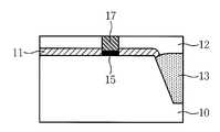
10 : 실리콘 기판11 : 질화막10
12 : 산화막13 : 소자절연막12
14 : 포토 레지스트15 : 게이트 절연막14
16 : 폴리실리콘17 : 게이트전극16
18 : 측벽 스페이서18: sidewall spacer
본 발명은 반도체 공정에서 게이트 전극 및 그 측벽 스페이서를 형성하는 방법에 관한 것으로, 보다 상세하게는 다마신(damascene)법을 사용하여 게이트 전극을 형성하고 및 게이트 전극 사이의 절연막을 습식각을 통하여 게이트 전극 측벽에 측벽(LDD: light doped drain) 스페이서를 형성하는 방법에 관한 것이다.BACKGROUND OF THE INVENTION 1. Field of the Invention The present invention relates to a method for forming a gate electrode and sidewall spacers thereof in a semiconductor process, and more particularly, to form a gate electrode using a damascene method and to wet the insulating film between the gate electrodes through wet etching. A light doped drain (LDD) spacer is formed on an electrode sidewall.
디바이스 크기가 축소되고 게이트 산화막이 20Å 이하로 얇아지면서 게이트 산화막의 균일성 및 그 특성형성 기술이 대단히 어렵고, 플라즈마 식각공정 또한 어려운 기술이기 때문에 반도체 소자를 형성하는 공정에서 미세한 게이트 전극의 형성법의 필요성이 증대하고 있는 현실이다. 특히, 게이트 전극 패터닝 공정과 게이트 측벽 스페이서 형성 공정을 살펴보면, 게이트 전극을 패터닝하는 공정에 있어서 식각기술은 종래에는 다음과 같은 기술을 적용하였다. 우선 확산법에 의하여 게이트 산화막을 형성하고, 그 상부에 게이트 전극으로 사용할 폴리실리콘을 증착한다. 다음으로 마스크 패터닝 공정을 거쳐 패터닝한 대로 프라즈마 건식각하여 게이트 전극을 형성한다. 이때, 1.15㎛ CMOS 기술에서는 이러한 게이트 형성시 N-MOS, P-MOS를 서로 다르게 하여 형성한다. 즉, N-MOS의 경우에는 P-MOS지역을 마스킹한 다음 N-MOS 지역에 인(phosphorous)를 먼저 이온 주입 공정으로 도핑을 하는 방법을 사용한다. 상기의 공정으로 인해 N-MOS와 P-MOS 지역의 게이트 전극막이 서로 다른 특징을 가지게 된다. 이러한 특성의 차이로 인해 다음과 같은 문제점이 발생한다. 첫째, 서로 다른 N-MOS 및 P-MOS 의 물성으로 인해 플라즈마 건식각시 서로 다른 식각속도로 인해 식각 형성이 서로 다르게 되는 문제가 발생한다. 둘째, 고도의 기술일수록 게이트 산화막이 얇기 때문에 먼저 식각되는 N-MOS 지역에서는 게이트 산화막이 P-MOS가 식각되는 동안 게이트 산화막을 뚫고 산화막 아래의 실리콘을 식각하는 문제가 발생한다. 즉, 과도식각이 너무 많으면 게이트 산화막에 어택(attack)을 입어 산화막의 펀치(punch)가 일어나고, 너무 적게 과도식각을 하게 되면 식각후 잔류물이 남게 되어 게이트 블릿지(bridge)를 발생하게 된다.As the device size is reduced and the gate oxide film is thinner than 20 kV, the uniformity and characterization technology of the gate oxide film is very difficult, and the plasma etching process is also difficult. Therefore, the necessity of forming a fine gate electrode in the process of forming a semiconductor device is required. It is an increasing reality. In particular, the gate electrode patterning process and the gate sidewall spacer forming process will be described. In the process of patterning the gate electrode, the etching technique has conventionally been applied to the following technique. First, a gate oxide film is formed by a diffusion method, and polysilicon to be used as a gate electrode is deposited thereon. Next, the gate electrode is formed by plasma dry etching as patterned through a mask patterning process. At this time, the N-MOS and the P-MOS are formed differently in the gate technology in the 1.15 탆 CMOS technology. In other words, in the case of N-MOS, the P-MOS region is masked and phosphorus (phosphorous) is first doped by an ion implantation process. Due to the above process, the gate electrode films in the N-MOS and P-MOS regions have different characteristics. This difference in characteristics causes the following problems. First, a problem arises in that the etching formation is different due to different etching speeds during plasma dry etching due to different N-MOS and P-MOS properties. Second, the higher the gate technology, the thinner the gate oxide layer is, so that in the N-MOS region, which is etched first, the gate oxide layer penetrates the gate oxide layer and etches the silicon under the oxide layer while the P-MOS is etched. That is, too much transient etching causes an attack on the gate oxide layer, causing a punch of the oxide layer, and too little excessive etching results in a residue after etching, resulting in a gate bridge.
다음으로 게이트 형성 후 소자를 형성하는 방법으로 게이트 전극 측벽에 측벽(LDD: lightly doped drain) 스페이서(spacer)를 형성하는 종래의 방법은 다음과 같다. 게이트 전극 위에 산화막과 질화막을 증착한 후 마스크 없이 블랭킷(blanket)으로 건식각 공정을 진행하는데, 플라즈마 건식각의 비등방성 식각 특성에 따라 게이트 전극 측벽에 절연, 질화막의 스페이서가 형성된다. 이러한 기존의 방법은 다음과 같은 문제점이 있다. 첫째, 스패이서 형성시 그 폭을 조절하기 어렵다는 문제점이다. 둘쩨, 플라즈마 건식각시 식각 불균일성 문제로 약간의 과도식각을 하게 되는데, 그 과도식각시 소스 드레인의 엑티브 영역에 어택을 가하여 리키지(leakage) 전류가 흐르는 문제점이다.Next, a conventional method of forming a lightly doped drain (LDD) spacer on a gate electrode sidewall by forming a device after gate formation is as follows. After depositing an oxide film and a nitride film on the gate electrode, a dry etching process is performed by using a blanket without a mask. Insulating and nitride spacers are formed on the sidewalls of the gate electrode according to the anisotropic etching characteristic of the plasma dry etching. This conventional method has the following problems. First, it is difficult to control the width when forming a spacer. Secondly, the plasma dry etching is slightly overetched due to the etching non-uniformity problem, which is a problem in that a leakage current flows by applying an attack to the active region of the source drain.
본 발명은 상기의 문제점을 해결하기 위한 것으로서, 게이트 전극형성에 있어서는 종래와 다르게 디마신법을 사용하여 게이트 패터닝을 제공하고, 측벽 스페이서 형성에 있어서는 습식각을 사용하여 형성하는 방법을 제공하는데 그 목적이 있다. 게이트 형성의 경우에는 게이트 전극형성에 있어서 다마신법을 이용하여 게이트 패터닝을 하는데, 먼저 산화막을 게이트 층의 두께로 증착한 다음 게이트 전극이 형성될 부분을 먼저 패터닝하여 플라즈마 건식각한다. 그런 다음 식각한 절연층에 게이트 산화막을 얇게 형성한 후 게이트 폴리실리콘을 증착하여 CMP 공정을 통하여 게이트 전극을 평탄화하는 방법으로 게이트 전극을 형성한다. 다음으로, 게이트 전극 측벽의 측벽 스페이서의 형성에 있어서는, 상기한 게이트 형성기술을 적용한 게이트 전극 사이의 절연막을 습식각 방법으로 측벽 스페이서를 형성한다.Disclosure of Invention The present invention is to solve the above problems, and in the formation of the gate electrode, a gate patterning is provided using a dimasine method, and a wet etching method is used to form sidewall spacers. have. In the case of gate formation, gate patterning is performed by using the damascene method in forming a gate electrode. First, an oxide film is deposited to a thickness of a gate layer, and then a portion where a gate electrode is to be formed is first patterned and plasma-etched. Thereafter, a thin gate oxide film is formed on the etched insulating layer, and then gate polysilicon is deposited to planarize the gate electrode through a CMP process. Next, in forming the sidewall spacers of the gate electrode sidewalls, the sidewall spacers are formed by a wet etching method between the insulating films between the gate electrodes to which the above-described gate forming technique is applied.
상기한 목적을 달성하기 위하여, 본 발명은 게이트 전극 및 측벽 스페이서를 형성하는 방법에 있어서, 반도체 기판상에 질화막 및 산화막의 적층구조를 형성하는 단계, 게이트 전극을 형성하고자 하는 부분을 레지스트를 이용한 마스크 리소그래피 공정으로 패터닝하는 단계, 게이트 전극을 형성하고자 하는 영역의 상기 산화막 및 질화막을 선택적으로 식각하여 상기 반도체 기판을 노출시키는 단계, 상기 반도체 기판의 노출 영역에 게이트 산화막을 형성하는 단계, 상기 반도체 기판의 전면에 폴리실리콘막을 형성하는 단계, 상기 산화막이 노출되도록 연마하여 게이트 전극을 형성하는 단계, 및 상기 산화막 및 질화막을 식각하여 상기 게이트 전극의 양측에 측벽 스페이서를 형성하는 단계를 포함하는 것을 특징으로 한다.In order to achieve the above object, the present invention provides a method for forming a gate electrode and sidewall spacers, the method comprising: forming a stacked structure of a nitride film and an oxide film on a semiconductor substrate, a mask using a resist to form the gate electrode Patterning in a lithography process, selectively etching the oxide film and nitride film in a region where a gate electrode is to be formed, exposing the semiconductor substrate, forming a gate oxide film in an exposed region of the semiconductor substrate, and Forming a polysilicon film on the entire surface, polishing the oxide film to expose the oxide film, and forming a gate electrode, and forming sidewall spacers on both sides of the gate electrode by etching the oxide film and the nitride film. .
상술한 목적 및 기타의 목적과 본 발명의 특징 및 이점은 첨부된 도면과 관련한 다음의 상세한 설명을 통하여 보다 분명해 질 것이다. 이하, 첨부된 도면을 참조하여 본 발명의 실시예를 상세히 설명하면 다음과 같다.The above and other objects and features and advantages of the present invention will become more apparent from the following detailed description taken in conjunction with the accompanying drawings. Hereinafter, exemplary embodiments of the present invention will be described in detail with reference to the accompanying drawings.
도 1a 내지 도 1f는 본 발명의 실시례에 따른 게이트 전극 및 측벽 스페이서 형성 공정을 도시하는 단면도이다.1A to 1F are cross-sectional views illustrating a gate electrode and sidewall spacer forming process according to an exemplary embodiment of the present invention.
먼저, 아이솔레이션 공정을 통하여 소자절연막(10)을 형성한 후 질화막(11)을 증착하고 그 상부에 게이트 전극을 형성하기 위한 산화막(12)을 증착하는 적층구조 형성 단계를 거친다.(도 1a 참조). 이때 질화막(11)을 증착하는 이유는 게이트 전극(17)형성을 위한 트렌치 건식각시 질화막(11)이 산화막(12)보다 식각속도가 느리게 함으로써 식각 종말의 역할을 하기 위해서이다. 이러한 식각 종말을 하지 않으면 산화막(12) 건식각시 하부층인 실리콘을 식각하여 하층 어택을 가할 수 있다. 바람직하게는, 질화막(11)의 두께는 200Å으로 할 수 있고, 질화막(11)의 상부에 증착되는 산화막(12)의 두께는 게이트 전극(17)의 높이인 2000Å으로 할 수 있다.First, after forming the
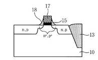
다음으로, 감광막을 이용하여 게이트 전극(17)이 될 부분을 패터닝하고, 상기 패턴에 따라 산화막(12) 및 질화막(11)을 선택식각하여 반도체 기판을 노출시키는 단계를 거친다(도 1b, 1C 참조). 이 때, 산화막(12)의 상부에 게이트 전극(17)이 형성될 부분을 마스크 리소그래피 공정으로 패터닝시 사용되는 레지스트(14)의 두께는 5000Å이하로 얇아도 충분하므로 게이트 전극(17)의 폭인 0.15㎛ 이하의 패터닝이 가능하다. 왜냐하면, 2000Å의 산화막을 식각하는 데 있어서, 산화막(12)과 레지스트(14)의 선택비가 2:1 이상이 되기 때문에 얇은 레지스트(14)로도 2000Å의 산화막(12)을 식각하는 것이 가능하기 때문이다. 바람직하게는, 마스크 패터닝 후에는 다음과 같은 조건으로 플라즈마 건식각을 한다. 이때 하부층의 실리콘(10)에 어택을 가하지 않기 위해서는 질화막(11)을 식각종말점으로 하고, 산화막(12)에 대한 질화막(11)의 선택비를 높게 하여야 한다.Next, the portion to be the
플라즈마 건식각의 조건은 첫 번째로 레지스트와 산화막의 1차 식각시의 챔버조건은 압력은 30mT, 챔버의 상부전극의 전력은 2200W, 하부전극은 1600W, 기체조성비는 18C4F8/10O2/420Ar, 식각시간은 70초, 상부전극과 하부전극의 거리는 21㎜, He압력은 상부가 10T, 하부가 35T, 상부온도는 30℃, 하부온도는 10℃, 외벽의 온도는 50℃로 하고, 식각조건은 산화막의 식각율은 분당 7600Å, 균일도(uniformity)는 5%미만, 레지스트의 식각률은 분당 1990Å, 레지스트에 대한 산화막의 선택비는 3.8, 질화막의 식각률은 초당 7.6Å, 질화막에 대한 산화막의 선택비는 16.7로 할 수 있다.The first condition for plasma dry etching is the chamber condition for the first etching of resist and oxide film, the pressure is 30mT, the upper electrode power is 2200W, the lower electrode is 1600W, and the gas composition ratio is 18C4 F8 / 10O2 / 420Ar, the etching time is 70 seconds, the distance between the upper electrode and the lower electrode is 21mm, the He pressure is 10T in the upper part, 35T in the lower part, the upper temperature is 30 ℃, the lower temperature is 10 ℃, the temperature of the outer wall is 50 ℃, The etching conditions of the oxide film were 7600Å / min, uniformity was less than 5%, the resistivity of the resist was 1990Å / min, the selectivity of the oxide to resist was 3.8, the etch rate of the nitride film was 7.6 의 / sec, and the oxide film The selection ratio may be 16.7.
두 번째로 산화막과 질화막의 2차 식각시의 챔버조건은 압력은 50mT, 챔버의 상부전극의 전력은 1000W, 하부전극은 200W, 기체조성비는 20CHP3/20O2/400Ar, 식각시간은 10초, 상부전극과 하부전극의 거리는 20㎜, He압력은 상부가 10T, 하부가 35T, 상부온도는 30℃, 하부온도는 10℃, 외벽의 온도는 50℃로 하고, 식각조건은 질화막의 식각율은 초당 18.8Å, 산화막의 식각률은 초당 13.3Å, 레지스트에 대한 산화막의 선택비는 1.4로 할 수 있다.Secondly, the chamber conditions for the second etching of the oxide and nitride films are 50mT in pressure, 1000W in the upper electrode power, 200W in the lower electrode, gas composition ratio 20CHP3 / 20O2 / 400Ar,
다음으로, 노출된 반도체 기판에 게이트 산화막(15)을 형성하는 단계를 거친다(도 1d참조). 바람직하게는, 증착되는 게이트 산화막(15)의 두께는 20Å으로 확산법을 이용하여 증착할 수 있다.Next, the
다음으로, 반도체 기판의 전면에 폴리실리콘막(16)을 형성하는 단계를 거친다(도 1e 참조). 바람직하게는, 증착되는 폴리실리콘막(16)의 두께는 7000Å으로 할 수 있다.Next, the
다음으로, 산화막(12)이 노출되도록 연마하여 게이트 전극(17)을 형성하는 단계를 거친다(도 1f 참조). 도시된 바와 같이 CMP 공정을 통하여 폴리실리콘막(16)을 평탄화하면, 선택식각된 부분에 채워진 폴리실리콘만 남게되는 데, 이 부분이 게이트 전극(17)이 된다.Next, the
다음으로, 산화막(12) 및 질화막(11)을 식각하여 상기 게이트 전극(17)의 양측에 측벽 스페이서(18)를 형성하는 단계를 거친다(도 1g 참조). 바람직하게는 측벽 스페이서(18)는 습식각을 통해 형성되는데, 산화막(12)은 BOE(buffered oxide etchant)로, 질화막(11)은 인산을 이용하여 식각한다. 상기 식각액을 통하여 질화막(11)이 드러나는 종말점까지 식각하게 되면 습식각은 등방성 식각특성으로 식각되므로 도시된 바와 같은 측벽 스페이서(18)를 형성할 수 있다. 또한 상기의 습식각의 과도식각시간에 따라 자유로이 측벽 스페이서(18)의 폭을 조절할 수 있다.Next, the
이상에서 설명한 바와 같이 본 발명에 따른 게이트 전극 및 측벽 스페이서형성 방법에 따르면, 게이트 전극의 식각형상을 다양한 반도체 장치에서 적절하게 선택할 수 있고, 측벽 스페이서는 습식극을 통하여 형성되므로 플라즈마 어택으로부터 보호할 수 있고 습식각의 과도식각시간을 조절함으로써 측벽 스페이서 폭을 조절할 수 있다.As described above, according to the method for forming the gate electrode and the sidewall spacer according to the present invention, the etching shape of the gate electrode can be appropriately selected in various semiconductor devices, and the sidewall spacers are formed through wet electrodes, thereby protecting them from plasma attack. And the sidewall spacer width can be adjusted by adjusting the transient etching time of the wet etching.
아울러 본 발명의 바람직한 실시예들은 예시의 목적을 위해 개시된 것이며, 당업자라면 본 발명의 사상과 범위 안에서 다양한 수정, 변경, 부가 등이 가능할 것이며, 이러한 수정 변경 등은 이하의 특허청구의 범위에 속하는 것으로 보아야 할 것이다.In addition, preferred embodiments of the present invention are disclosed for the purpose of illustration, those skilled in the art will be able to make various modifications, changes, additions, etc. within the spirit and scope of the present invention, such modifications and modifications belong to the scope of the claims You will have to look.
Claims (13)
Translated fromKoreanPriority Applications (1)
| Application Number | Priority Date | Filing Date | Title |
|---|---|---|---|
| KR1020010038045AKR100785862B1 (en) | 2001-06-29 | 2001-06-29 | Gate electrode and sidewall spacer formation method using damascene |
Applications Claiming Priority (1)
| Application Number | Priority Date | Filing Date | Title |
|---|---|---|---|
| KR1020010038045AKR100785862B1 (en) | 2001-06-29 | 2001-06-29 | Gate electrode and sidewall spacer formation method using damascene |
Publications (2)
| Publication Number | Publication Date |
|---|---|
| KR20030002446A KR20030002446A (en) | 2003-01-09 |
| KR100785862B1true KR100785862B1 (en) | 2007-12-13 |
Family
ID=27712174
Family Applications (1)
| Application Number | Title | Priority Date | Filing Date |
|---|---|---|---|
| KR1020010038045AExpired - Fee RelatedKR100785862B1 (en) | 2001-06-29 | 2001-06-29 | Gate electrode and sidewall spacer formation method using damascene |
Country Status (1)
| Country | Link |
|---|---|
| KR (1) | KR100785862B1 (en) |
Citations (1)
| Publication number | Priority date | Publication date | Assignee | Title |
|---|---|---|---|---|
| KR20000024755A (en)* | 1998-10-01 | 2000-05-06 | 윤종용 | Method for forming gate electrode of semiconductor device |
- 2001
- 2001-06-29KRKR1020010038045Apatent/KR100785862B1/ennot_activeExpired - Fee Related
Patent Citations (1)
| Publication number | Priority date | Publication date | Assignee | Title |
|---|---|---|---|---|
| KR20000024755A (en)* | 1998-10-01 | 2000-05-06 | 윤종용 | Method for forming gate electrode of semiconductor device |
Non-Patent Citations (1)
| Title |
|---|
| 한국공개특허번호 10-2000-0024755 |
Also Published As
| Publication number | Publication date |
|---|---|
| KR20030002446A (en) | 2003-01-09 |
Similar Documents
| Publication | Publication Date | Title |
|---|---|---|
| JPH01290236A (en) | Method of levelling wide trench | |
| JPH03291921A (en) | Manufacture of ic | |
| KR100541817B1 (en) | Dual gate insulating film formation method | |
| KR100785862B1 (en) | Gate electrode and sidewall spacer formation method using damascene | |
| US6610604B1 (en) | Method of forming small transistor gates by using self-aligned reverse spacer as a hard mask | |
| KR100585084B1 (en) | Self-aligned contact etching method of semiconductor device | |
| KR100376985B1 (en) | Forming method for contact of semiconductor device | |
| KR100670652B1 (en) | Method for forming contact plug of semiconductor device | |
| KR20000045437A (en) | Method for forming self aligned contact of semiconductor device | |
| KR20000043904A (en) | Method for forming contact hole of semiconductor device | |
| KR20010073304A (en) | Method for forming fine pattern in semiconductor device | |
| KR100367490B1 (en) | Method for forming contact hole of semiconductor device | |
| KR100223825B1 (en) | Method of forming an element isolation region in a semiconductor device | |
| JPH04317357A (en) | Manufacture of semiconductor device | |
| KR20040008600A (en) | Method for forming a contact hole in semiconductor memory device | |
| KR100291417B1 (en) | Manufacturing Method for Isolation of Semiconductor Device | |
| KR20000044889A (en) | Method for forming bit line plug of semiconductor device | |
| JP2002100670A (en) | Semiconductor device and its manufacturing method | |
| KR100370132B1 (en) | Method for fabricating semiconductor device | |
| KR100277861B1 (en) | Plug Formation Method for Semiconductor Devices | |
| JPH10242275A (en) | Manufacture of semiconductor device | |
| KR100413043B1 (en) | Gate electrode formation method of semiconductor device | |
| KR20020001335A (en) | Method for manufacturing semiconductor for planarization in damascene gate process | |
| KR20010084778A (en) | integrated circuit semiconductor device included aluminum oxide in gate insulating layer and manufacturing method thereof | |
| KR20060002182A (en) | Method of forming a semiconductor device |
Legal Events
| Date | Code | Title | Description |
|---|---|---|---|
| PA0109 | Patent application | St.27 status event code:A-0-1-A10-A12-nap-PA0109 | |
| PG1501 | Laying open of application | St.27 status event code:A-1-1-Q10-Q12-nap-PG1501 | |
| N231 | Notification of change of applicant | ||
| PN2301 | Change of applicant | St.27 status event code:A-3-3-R10-R13-asn-PN2301 St.27 status event code:A-3-3-R10-R11-asn-PN2301 | |
| R17-X000 | Change to representative recorded | St.27 status event code:A-3-3-R10-R17-oth-X000 | |
| PN2301 | Change of applicant | St.27 status event code:A-3-3-R10-R13-asn-PN2301 St.27 status event code:A-3-3-R10-R11-asn-PN2301 | |
| R17-X000 | Change to representative recorded | St.27 status event code:A-3-3-R10-R17-oth-X000 | |
| A201 | Request for examination | ||
| PA0201 | Request for examination | St.27 status event code:A-1-2-D10-D11-exm-PA0201 | |
| E902 | Notification of reason for refusal | ||
| PE0902 | Notice of grounds for rejection | St.27 status event code:A-1-2-D10-D21-exm-PE0902 | |
| P11-X000 | Amendment of application requested | St.27 status event code:A-2-2-P10-P11-nap-X000 | |
| P13-X000 | Application amended | St.27 status event code:A-2-2-P10-P13-nap-X000 | |
| E701 | Decision to grant or registration of patent right | ||
| PE0701 | Decision of registration | St.27 status event code:A-1-2-D10-D22-exm-PE0701 | |
| GRNT | Written decision to grant | ||
| PR0701 | Registration of establishment | St.27 status event code:A-2-4-F10-F11-exm-PR0701 | |
| PR1002 | Payment of registration fee | St.27 status event code:A-2-2-U10-U11-oth-PR1002 Fee payment year number:1 | |
| PG1601 | Publication of registration | St.27 status event code:A-4-4-Q10-Q13-nap-PG1601 | |
| PR1001 | Payment of annual fee | St.27 status event code:A-4-4-U10-U11-oth-PR1001 Fee payment year number:4 | |
| PR1001 | Payment of annual fee | St.27 status event code:A-4-4-U10-U11-oth-PR1001 Fee payment year number:5 | |
| FPAY | Annual fee payment | Payment date:20121121 Year of fee payment:6 | |
| PR1001 | Payment of annual fee | St.27 status event code:A-4-4-U10-U11-oth-PR1001 Fee payment year number:6 | |
| FPAY | Annual fee payment | Payment date:20131118 Year of fee payment:7 | |
| PR1001 | Payment of annual fee | St.27 status event code:A-4-4-U10-U11-oth-PR1001 Fee payment year number:7 | |
| FPAY | Annual fee payment | Payment date:20141119 Year of fee payment:8 | |
| PR1001 | Payment of annual fee | St.27 status event code:A-4-4-U10-U11-oth-PR1001 Fee payment year number:8 | |
| FPAY | Annual fee payment | Payment date:20151118 Year of fee payment:9 | |
| PR1001 | Payment of annual fee | St.27 status event code:A-4-4-U10-U11-oth-PR1001 Fee payment year number:9 | |
| FPAY | Annual fee payment | Payment date:20161118 Year of fee payment:10 | |
| PR1001 | Payment of annual fee | St.27 status event code:A-4-4-U10-U11-oth-PR1001 Fee payment year number:10 | |
| FPAY | Annual fee payment | Payment date:20171117 Year of fee payment:11 | |
| PR1001 | Payment of annual fee | St.27 status event code:A-4-4-U10-U11-oth-PR1001 Fee payment year number:11 | |
| FPAY | Annual fee payment | Payment date:20181120 Year of fee payment:12 | |
| PR1001 | Payment of annual fee | St.27 status event code:A-4-4-U10-U11-oth-PR1001 Fee payment year number:12 | |
| P22-X000 | Classification modified | St.27 status event code:A-4-4-P10-P22-nap-X000 | |
| FPAY | Annual fee payment | Payment date:20191119 Year of fee payment:13 | |
| PR1001 | Payment of annual fee | St.27 status event code:A-4-4-U10-U11-oth-PR1001 Fee payment year number:13 | |
| PC1903 | Unpaid annual fee | St.27 status event code:A-4-4-U10-U13-oth-PC1903 Not in force date:20201208 Payment event data comment text:Termination Category : DEFAULT_OF_REGISTRATION_FEE | |
| R18-X000 | Changes to party contact information recorded | St.27 status event code:A-5-5-R10-R18-oth-X000 | |
| PC1903 | Unpaid annual fee | St.27 status event code:N-4-6-H10-H13-oth-PC1903 Ip right cessation event data comment text:Termination Category : DEFAULT_OF_REGISTRATION_FEE Not in force date:20201208 | |
| PN2301 | Change of applicant | St.27 status event code:A-5-5-R10-R13-asn-PN2301 St.27 status event code:A-5-5-R10-R11-asn-PN2301 | |
| P22-X000 | Classification modified | St.27 status event code:A-4-4-P10-P22-nap-X000 |