KR100784103B1 - Semiconductor package - Google Patents
Semiconductor packageDownload PDFInfo
- Publication number
- KR100784103B1 KR100784103B1KR1020010023163AKR20010023163AKR100784103B1KR 100784103 B1KR100784103 B1KR 100784103B1KR 1020010023163 AKR1020010023163 AKR 1020010023163AKR 20010023163 AKR20010023163 AKR 20010023163AKR 100784103 B1KR100784103 B1KR 100784103B1
- Authority
- KR
- South Korea
- Prior art keywords
- semiconductor chip
- chip
- integrated circuit
- semiconductor
- conductive pattern
- Prior art date
- Legal status (The legal status is an assumption and is not a legal conclusion. Google has not performed a legal analysis and makes no representation as to the accuracy of the status listed.)
- Expired - Lifetime
Links
Images

Classifications
- H—ELECTRICITY
- H01—ELECTRIC ELEMENTS
- H01L—SEMICONDUCTOR DEVICES NOT COVERED BY CLASS H10
- H01L25/00—Assemblies consisting of a plurality of semiconductor or other solid state devices
- H01L25/03—Assemblies consisting of a plurality of semiconductor or other solid state devices all the devices being of a type provided for in a single subclass of subclasses H10B, H10D, H10F, H10H, H10K or H10N, e.g. assemblies of rectifier diodes
- H01L25/04—Assemblies consisting of a plurality of semiconductor or other solid state devices all the devices being of a type provided for in a single subclass of subclasses H10B, H10D, H10F, H10H, H10K or H10N, e.g. assemblies of rectifier diodes the devices not having separate containers
- H01L25/065—Assemblies consisting of a plurality of semiconductor or other solid state devices all the devices being of a type provided for in a single subclass of subclasses H10B, H10D, H10F, H10H, H10K or H10N, e.g. assemblies of rectifier diodes the devices not having separate containers the devices being of a type provided for in group H10D89/00
- H01L25/0657—Stacked arrangements of devices
- H—ELECTRICITY
- H01—ELECTRIC ELEMENTS
- H01L—SEMICONDUCTOR DEVICES NOT COVERED BY CLASS H10
- H01L2224/00—Indexing scheme for arrangements for connecting or disconnecting semiconductor or solid-state bodies and methods related thereto as covered by H01L24/00
- H01L2224/01—Means for bonding being attached to, or being formed on, the surface to be connected, e.g. chip-to-package, die-attach, "first-level" interconnects; Manufacturing methods related thereto
- H01L2224/10—Bump connectors; Manufacturing methods related thereto
- H01L2224/15—Structure, shape, material or disposition of the bump connectors after the connecting process
- H01L2224/16—Structure, shape, material or disposition of the bump connectors after the connecting process of an individual bump connector
- H01L2224/161—Disposition
- H01L2224/16151—Disposition the bump connector connecting between a semiconductor or solid-state body and an item not being a semiconductor or solid-state body, e.g. chip-to-substrate, chip-to-passive
- H01L2224/16221—Disposition the bump connector connecting between a semiconductor or solid-state body and an item not being a semiconductor or solid-state body, e.g. chip-to-substrate, chip-to-passive the body and the item being stacked
- H01L2224/16225—Disposition the bump connector connecting between a semiconductor or solid-state body and an item not being a semiconductor or solid-state body, e.g. chip-to-substrate, chip-to-passive the body and the item being stacked the item being non-metallic, e.g. insulating substrate with or without metallisation
- H—ELECTRICITY
- H01—ELECTRIC ELEMENTS
- H01L—SEMICONDUCTOR DEVICES NOT COVERED BY CLASS H10
- H01L2224/00—Indexing scheme for arrangements for connecting or disconnecting semiconductor or solid-state bodies and methods related thereto as covered by H01L24/00
- H01L2224/01—Means for bonding being attached to, or being formed on, the surface to be connected, e.g. chip-to-package, die-attach, "first-level" interconnects; Manufacturing methods related thereto
- H01L2224/26—Layer connectors, e.g. plate connectors, solder or adhesive layers; Manufacturing methods related thereto
- H01L2224/31—Structure, shape, material or disposition of the layer connectors after the connecting process
- H01L2224/32—Structure, shape, material or disposition of the layer connectors after the connecting process of an individual layer connector
- H01L2224/321—Disposition
- H01L2224/32135—Disposition the layer connector connecting between different semiconductor or solid-state bodies, i.e. chip-to-chip
- H01L2224/32145—Disposition the layer connector connecting between different semiconductor or solid-state bodies, i.e. chip-to-chip the bodies being stacked
- H—ELECTRICITY
- H01—ELECTRIC ELEMENTS
- H01L—SEMICONDUCTOR DEVICES NOT COVERED BY CLASS H10
- H01L2224/00—Indexing scheme for arrangements for connecting or disconnecting semiconductor or solid-state bodies and methods related thereto as covered by H01L24/00
- H01L2224/01—Means for bonding being attached to, or being formed on, the surface to be connected, e.g. chip-to-package, die-attach, "first-level" interconnects; Manufacturing methods related thereto
- H01L2224/42—Wire connectors; Manufacturing methods related thereto
- H01L2224/47—Structure, shape, material or disposition of the wire connectors after the connecting process
- H01L2224/48—Structure, shape, material or disposition of the wire connectors after the connecting process of an individual wire connector
- H01L2224/4805—Shape
- H01L2224/4809—Loop shape
- H01L2224/48091—Arched
- H—ELECTRICITY
- H01—ELECTRIC ELEMENTS
- H01L—SEMICONDUCTOR DEVICES NOT COVERED BY CLASS H10
- H01L2224/00—Indexing scheme for arrangements for connecting or disconnecting semiconductor or solid-state bodies and methods related thereto as covered by H01L24/00
- H01L2224/01—Means for bonding being attached to, or being formed on, the surface to be connected, e.g. chip-to-package, die-attach, "first-level" interconnects; Manufacturing methods related thereto
- H01L2224/42—Wire connectors; Manufacturing methods related thereto
- H01L2224/47—Structure, shape, material or disposition of the wire connectors after the connecting process
- H01L2224/48—Structure, shape, material or disposition of the wire connectors after the connecting process of an individual wire connector
- H01L2224/481—Disposition
- H01L2224/48151—Connecting between a semiconductor or solid-state body and an item not being a semiconductor or solid-state body, e.g. chip-to-substrate, chip-to-passive
- H01L2224/48221—Connecting between a semiconductor or solid-state body and an item not being a semiconductor or solid-state body, e.g. chip-to-substrate, chip-to-passive the body and the item being stacked
- H01L2224/48225—Connecting between a semiconductor or solid-state body and an item not being a semiconductor or solid-state body, e.g. chip-to-substrate, chip-to-passive the body and the item being stacked the item being non-metallic, e.g. insulating substrate with or without metallisation
- H01L2224/48227—Connecting between a semiconductor or solid-state body and an item not being a semiconductor or solid-state body, e.g. chip-to-substrate, chip-to-passive the body and the item being stacked the item being non-metallic, e.g. insulating substrate with or without metallisation connecting the wire to a bond pad of the item
- H—ELECTRICITY
- H01—ELECTRIC ELEMENTS
- H01L—SEMICONDUCTOR DEVICES NOT COVERED BY CLASS H10
- H01L2224/00—Indexing scheme for arrangements for connecting or disconnecting semiconductor or solid-state bodies and methods related thereto as covered by H01L24/00
- H01L2224/01—Means for bonding being attached to, or being formed on, the surface to be connected, e.g. chip-to-package, die-attach, "first-level" interconnects; Manufacturing methods related thereto
- H01L2224/42—Wire connectors; Manufacturing methods related thereto
- H01L2224/47—Structure, shape, material or disposition of the wire connectors after the connecting process
- H01L2224/48—Structure, shape, material or disposition of the wire connectors after the connecting process of an individual wire connector
- H01L2224/481—Disposition
- H01L2224/48151—Connecting between a semiconductor or solid-state body and an item not being a semiconductor or solid-state body, e.g. chip-to-substrate, chip-to-passive
- H01L2224/48221—Connecting between a semiconductor or solid-state body and an item not being a semiconductor or solid-state body, e.g. chip-to-substrate, chip-to-passive the body and the item being stacked
- H01L2224/48245—Connecting between a semiconductor or solid-state body and an item not being a semiconductor or solid-state body, e.g. chip-to-substrate, chip-to-passive the body and the item being stacked the item being metallic
- H01L2224/48247—Connecting between a semiconductor or solid-state body and an item not being a semiconductor or solid-state body, e.g. chip-to-substrate, chip-to-passive the body and the item being stacked the item being metallic connecting the wire to a bond pad of the item
- H—ELECTRICITY
- H01—ELECTRIC ELEMENTS
- H01L—SEMICONDUCTOR DEVICES NOT COVERED BY CLASS H10
- H01L2224/00—Indexing scheme for arrangements for connecting or disconnecting semiconductor or solid-state bodies and methods related thereto as covered by H01L24/00
- H01L2224/73—Means for bonding being of different types provided for in two or more of groups H01L2224/10, H01L2224/18, H01L2224/26, H01L2224/34, H01L2224/42, H01L2224/50, H01L2224/63, H01L2224/71
- H01L2224/732—Location after the connecting process
- H01L2224/73251—Location after the connecting process on different surfaces
- H01L2224/73253—Bump and layer connectors
- H—ELECTRICITY
- H01—ELECTRIC ELEMENTS
- H01L—SEMICONDUCTOR DEVICES NOT COVERED BY CLASS H10
- H01L2224/00—Indexing scheme for arrangements for connecting or disconnecting semiconductor or solid-state bodies and methods related thereto as covered by H01L24/00
- H01L2224/73—Means for bonding being of different types provided for in two or more of groups H01L2224/10, H01L2224/18, H01L2224/26, H01L2224/34, H01L2224/42, H01L2224/50, H01L2224/63, H01L2224/71
- H01L2224/732—Location after the connecting process
- H01L2224/73251—Location after the connecting process on different surfaces
- H01L2224/73265—Layer and wire connectors
- H—ELECTRICITY
- H01—ELECTRIC ELEMENTS
- H01L—SEMICONDUCTOR DEVICES NOT COVERED BY CLASS H10
- H01L2924/00—Indexing scheme for arrangements or methods for connecting or disconnecting semiconductor or solid-state bodies as covered by H01L24/00
- H01L2924/15—Details of package parts other than the semiconductor or other solid state devices to be connected
- H01L2924/151—Die mounting substrate
- H01L2924/153—Connection portion
- H01L2924/1531—Connection portion the connection portion being formed only on the surface of the substrate opposite to the die mounting surface
- H01L2924/15311—Connection portion the connection portion being formed only on the surface of the substrate opposite to the die mounting surface being a ball array, e.g. BGA
- H—ELECTRICITY
- H01—ELECTRIC ELEMENTS
- H01L—SEMICONDUCTOR DEVICES NOT COVERED BY CLASS H10
- H01L2924/00—Indexing scheme for arrangements or methods for connecting or disconnecting semiconductor or solid-state bodies as covered by H01L24/00
- H01L2924/15—Details of package parts other than the semiconductor or other solid state devices to be connected
- H01L2924/161—Cap
- H01L2924/162—Disposition
- H01L2924/16235—Connecting to a semiconductor or solid-state bodies, i.e. cap-to-chip
- H—ELECTRICITY
- H01—ELECTRIC ELEMENTS
- H01L—SEMICONDUCTOR DEVICES NOT COVERED BY CLASS H10
- H01L2924/00—Indexing scheme for arrangements or methods for connecting or disconnecting semiconductor or solid-state bodies as covered by H01L24/00
- H01L2924/15—Details of package parts other than the semiconductor or other solid state devices to be connected
- H01L2924/181—Encapsulation
- H—ELECTRICITY
- H01—ELECTRIC ELEMENTS
- H01L—SEMICONDUCTOR DEVICES NOT COVERED BY CLASS H10
- H01L2924/00—Indexing scheme for arrangements or methods for connecting or disconnecting semiconductor or solid-state bodies as covered by H01L24/00
- H01L2924/19—Details of hybrid assemblies other than the semiconductor or other solid state devices to be connected
- H01L2924/191—Disposition
- H01L2924/19101—Disposition of discrete passive components
- H01L2924/19107—Disposition of discrete passive components off-chip wires
Landscapes
- Engineering & Computer Science (AREA)
- Power Engineering (AREA)
- Microelectronics & Electronic Packaging (AREA)
- Physics & Mathematics (AREA)
- Condensed Matter Physics & Semiconductors (AREA)
- General Physics & Mathematics (AREA)
- Computer Hardware Design (AREA)
- Light Receiving Elements (AREA)
Abstract
Translated fromKoreanDescription
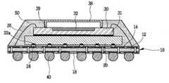
Translated fromKorean도 1은 본 발명에 따른 반도체 패키지의 제1실시예를 나타내는 단면도,1 is a cross-sectional view showing a first embodiment of a semiconductor package according to the present invention;
도 2는 본 발명에 따른 반도체 패키지의 제2실시예를 나타내는 단면도.2 is a cross-sectional view showing a second embodiment of a semiconductor package according to the present invention.
<도면의 주요 부분에 대한 부호의 설명><Explanation of symbols for main parts of the drawings>
10 : 부재14 : 전도성패턴10
20 : 하부 칩24 : 금속범프20: lower chip 24: metal bump
26 : 와이어30 : 광집적 회로 반도체 칩26: wire 30: integrated circuit semiconductor chip
32 : 광검출부38 : 글래스32: photodetector 38: glass
40 : 인출단자50 : 몰딩수지
40: withdrawal terminal 50: molding resin
본 발명은 반도체 패키지에 관한 것으로서, 더욱 상세하게는 광신호를 수신 연산하는 광집적 회로 반도체 칩과, 임의의 회로설계에 따라 신호 연산을 하는 반도체 칩이 상하로 적층된 구조의 반도체 패키지에 관한 것이다.The present invention relates to a semiconductor package, and more particularly, to a semiconductor package having a structure in which an optical integrated circuit semiconductor chip for receiving and calculating an optical signal and a semiconductor chip for signal calculation according to an arbitrary circuit design are stacked up and down. .
일반적으로 최근에 개발되는 전자통신기기들은 제조기술의 집약적인 발달과 함께 고기능화의 요구로 인하여, 메모리 및 연산을 위한 반도체 칩뿐만 아니라, 특정 기능을 구현하기 위한 반도체 칩들을 필요로 하고 있다.In general, recently developed electronic communication devices, due to the intensive development of manufacturing technology and the demand for high functionalization, require not only semiconductor chips for memory and operation, but also semiconductor chips for implementing specific functions.
그 예로서, 빛의 속성에 대하여 각종 변환처리를 수행하는 광집적 회로 반도체 칩이 제조되고 있는 바, 이러한 반도체 칩은 광검파기(Optical Detector)나, 카메라와 같은 광학기기 등에서 빛의 강도, 주파수, 위상 등의 정보를 전기적 신호로 변환하는 광정보처리를 수행하게 된다.As an example, an optical integrated circuit semiconductor chip which performs various conversion processing on the property of light has been manufactured. Such a semiconductor chip is used in an optical detector or an optical device such as a camera. Optical information processing for converting information such as a phase into an electrical signal is performed.
최근에는 이러한 광집적 회로 반도체 칩을 이용한 각종 전자기기들이 점차 고기능화되고 소형화됨에 따라, 보다 고집적화된 반도체 칩을 필요로 하게 되었고, 필요에 따라서는 다른 반도체 칩과의 통합된 기능을 수행하도록 설계되고 있다.Recently, as various electronic devices using the optical integrated circuit semiconductor chip have been increasingly functionalized and miniaturized, a more highly integrated semiconductor chip is needed, and it is designed to perform an integrated function with other semiconductor chips as necessary. .
종래에는 광집적 회로 반도체 칩의 패키지를 제조할 시, 내부에 하나의 광집적 회로 반도체 칩만을 실장하여 제조되고 있는 바, 이는 고도의 복잡한 신호 연산을 광집적 회로 반도체 칩에서 모두 수용하는데 한계가 있고, 마더보드상에 통합된 기능의 반도체 패키지를 별도로 실장하여야 하는 문제점이 있었다.Conventionally, when manufacturing a package of a photonic integrated circuit semiconductor chip, only one photonic integrated circuit semiconductor chip is mounted therein, which is limited in accommodating highly complex signal operations in the photonic integrated circuit semiconductor chip. However, there has been a problem in that a semiconductor package having integrated functions on a motherboard must be separately mounted.
이와 같이, 광집적 회로 반도체 칩이 적용된 패키지가 다른 반도체 패키지와 함께 통합된 기능을 수행하기 위하여 함께 실장되어야 함은 마더보드에 대한 전체적인 실장 면적을 크게 하고, 전자 통신기기의 소형화 추세에 역행하는 요인이 된다.
As such, the package in which the integrated circuit semiconductor chip is applied must be mounted together to perform an integrated function together with other semiconductor packages, thereby increasing the overall mounting area of the motherboard and counteracting the trend toward miniaturization of electronic communication devices. Becomes
따라서, 본 발명은 상기와 같은 문제점을 해결하기 위하여 발명한 것으로서, 부재상에 일반적인 신호 연산용 회로가 집적된 하부 칩이 플립칩 본딩되거나 와이어 본딩되어 실장되고, 하부 칩의 상면에 광집적 회로 반도체 칩이 와이어 본딩되어 적층된 반도체 패키지를 제공하는데 그 목적이 있다. Accordingly, the present invention has been invented to solve the above problems, and a lower chip in which a general signal calculating circuit is integrated on a member is mounted by flip chip bonding or wire bonding, and an optical integrated circuit semiconductor on an upper surface of the lower chip. An object of the present invention is to provide a semiconductor package in which chips are wire bonded and stacked.
본 발명은 광집적 회로 반도체 칩이 하부 칩 상면에 적층된 구조의 반도체 패키지를 제공함으로써, 하나의 칩으로 통합시키기 어려운 복합기능을 하나의 패키지에 의하여 구현 가능하게 하고, 광신호의 변환 처리를 더욱 신속하게 진행할 수 있으며, 마더보드상에서 부품의 전체적인 실장면적을 최소화할 수 있는 잇점을 제공하게 된다.
The present invention provides a semiconductor package having a structure in which an optical integrated circuit semiconductor chip is stacked on an upper surface of a lower chip, thereby enabling a single function to realize a complex function that is difficult to integrate into one chip, and to further convert optical signals. This can be done quickly and offers the advantage of minimizing the overall mounting area of components on the motherboard.
이하, 첨부도면을 참조하여 본 발명을 설명하면 다음과 같다.Hereinafter, the present invention will be described with reference to the accompanying drawings.
본 발명에 따른 반도체 패키지는: 베이스층을 이루는 절연수지층(12)상에 전도성패턴(14)이 에칭으로 형성된 부재(10)와; 상기 부재(10)의 전도성패턴(14)과 신호 교환 가능하게 부착되는 하부 칩(20)과; 상기 부재(10)의 전도성패턴(14)과 상기 하부 칩(20)의 본딩패드간에 신호 교환 가능하게 융착된 범프(24)와; 상기 하부 칩(20)의 상면에 접착력을 갖는 접착수단(31)에 의하여 부착된 광집적 회로 반도체 칩(30)과; 상기 광집적 회로 반도체 칩(30)의 광검출부(32)를 덮으면서 부착되는 빛 투과수단인 글래스와; 상기 빛 투과수단의 외측으로 형성된 상기 광집적 회로 반도체 칩(30)의 본딩패드와, 상기 부재(10)의 와이어 본딩용 전도성패턴간에 연결된 와이어(26)와; 상기 부재(10) 저면의 인출단자 부착용 전도성패턴에 신호 교환 가능하게 융착된 다수개의 인출단자(40)와; 상기 각 반도체 칩(20, 30)과 와이어(26)와 범프(24)를 포함하면서 부재의 상면에 걸쳐 몰딩된 수지(50)로 구성된 것을 특징으로 한다.A semiconductor package according to the present invention includes: a
본 발명의 다른 실시예에서, 상기 하부 칩(20)의 본딩패드와 상기 부재(10)간의 접속수단을 상기 범프(24)대신 와이어(26)로 연결 가능한 것을 특징으로 한다.In another embodiment of the present invention, it is possible to connect the connecting means between the bonding pad of the
여기서 본 발명의 실시예로서, 첨부한 도면을 참조로 더욱 상세하게 설명하면 다음과 같다.Here, as an embodiment of the present invention, it will be described in more detail with reference to the accompanying drawings as follows.
첨부한 도 1은 본 발명에 따른 반도체 패키지의 제1실시예를 나타내는 단면도이다.1 is a cross-sectional view showing a first embodiment of a semiconductor package according to the present invention.
도 1에 도시한 바와 같이, 본 발명의 반도체 패키지는 하부 칩(20)의 상면에 광집적 회로 반도체 칩(30)이 적층된 칩 스택형 반도체 패키지로서, 부재(10)상에 실장된 하부 칩(20)의 상면에 광검출부를 포함하는 광집적 회로 반도체 칩(30)이 적층된 구조로 되어 있다.As shown in FIG. 1, the semiconductor package of the present invention is a chip stack type semiconductor package in which an optical integrated
본 발명의 반도체 패키지에서, 상기 부재(10)는 인쇄회로기판 또는 회로필름등의 부재를 모두 이용 가능하다.In the semiconductor package of the present invention, the
상기 부재(10)는 베이스층인 절연수지층(12)의 양면에 전도성패턴(14)이 에칭 처리되어 형성된 것으로서, 이 전도성패턴(14)의 노출된 본딩영역과 실장된 각 반도체 칩(20, 30)의 본딩패드간에 신호의 입/출력이 이루어지게 된다.The
본 발명의 제1실시예에서, 상기 하부 칩(20)은 부재(10)상에서 플립 칩(flip chip) 본딩하여 실장되는데, 이를 좀 더 상세하게 설명하면, 하부 칩(20)을 다수개의 본딩패드(22a)가 부재(10)를 향하도록 한 후, 상기 부재(10)에 형성되어 있는 전도성 패턴의 본딩영역에 부착되도록 한다.In the first embodiment of the present invention, the
이때, 상기 하부 칩(20)의 본딩패드와 상기 부재(10)의 전도성패턴은 금속범프(24)로 연결시키고, 이 범프(24)로 인하여 상기 부재(10)의 전도성패턴(14)과 상기 하부 칩(20)의 본딩패드(22a)간은 전기적인 신호 교환이 가능한 상태가 된다.In this case, the bonding pad of the
여기서, 상기 광집적 회로 반도체 칩(30)이 소정의 접착수단(31)을 이용하여상기 하부 칩(20)의 상면에 부착되고, 빛 투과수단이 광검출부(32)를 포함하는 상기 광집적 회로 반도체 칩(30)의 상면을 덮으면서 부착되는 바, 상기 빛 투과수단의 예로서, 덮개형의 글래스(38)를 이용하는 것이 가장 바람직하다.Here, the optical integrated
좀 더 상세하게는, 상기 글래스(38)는 내부가 밀폐되도록 접착수단(39)에 의하여 상기 광집적 회로 반도체 칩(30)의 상면에 부착되는데, 이는 몰딩공정시 상기 글래스(38)가 움직이지 않도록 하고 내부에 몰딩수지가 유입되는 것을 막기 위함이다.More specifically, the
특히, 상기 글래스(38)를 광검출부(32)를 포함하는 상기 광집적 회로 반도체 칩(30)의 상면에 부착하되, 광집적 회로 반도체 칩(30)의 본딩패드 안쪽 영역을 덮으면서 부착되기 때문에, 광집적 회로 반도체 칩(30)의 본딩패드는 글래스(38)에 의하여 덮혀지지 않은 상태가 된다.In particular, the
이에, 상기 글래스(38)의 외측으로 위치된 광집적 회로 반도체 칩(30)의 본딩패드와, 상기 부재(10)의 와이어 본딩용 전도성패턴간을 와이어(26)로 연결하여, 신호의 입/출력이 이루어지게 된다. Accordingly, a
다음으로, 상기 하부 칩(20) 및 광집적 회로 반도체 칩(30), 그리고 상기 범프(24)와 와이어(26)를 포함하면서 부재(10)의 상면에 걸쳐 수지(50)로 몰딩을 하게 되는데, 이때 광집적 회로 반도체 칩(30)에서 광신호를 수신할 수 있도록 상기 글래스(38)의 표면은 외부로 노출된 상태가 된다.Next, the
물론, 상기 몰딩수지(50)의 높이와 글래스(38)의 표면 높이는 동일한 높이가 되도록 하는 것이 바람직하다.Of course, it is preferable that the height of the
또한, 상기 부재(10) 저면에 형성된 인출단자 부착용 전도성패턴에 각 반도체 칩(20, 30)의 신호를 외부로 입/출력할 수 있도록 다수개의 인출단자(40)가 융착되는 바, 이 인출단자(40)는 솔더 재질의 솔더볼을 융착시키는 것이 바람직하다.In addition, a plurality of
이와 같이, 본 발명의 반도체 패키지는 상기 글래스를 통하여 광신호를 수신하는 광집적 회로 반도체 칩(30)과, 임의의 회로설계에 따라 신호 연산을 하는 하부 칩(20)을 상하로 적층하여 제조된 것으로서, 예를들면 상기 광집적 회로 반도체 칩(30)은 광신호를 전기적인 신호로 변환하는 역할만을 하게 하고, 실질적인 연산 기능을 하부 칩에서 담당하게 함으로써, 전기적인 수행 성능을 향상시킬 수 있고, 회로의 연산 동작이 정밀하게 수행될 수 있으며, 고집적도를 실현하는 동시에 마더보드에 대한 실장면적을 줄일 수 있게 된다.As described above, the semiconductor package of the present invention is manufactured by stacking an optical integrated
첨부한 도 2는 본 발명에 따른 반도체 패키지의 제2실시예를 나타내는 단면도이다.2 is a cross-sectional view showing a second embodiment of a semiconductor package according to the present invention.
상기 제2실시예의 반도체 패키지는 상술한 제1실시예의 반도체 패키지의 구 성과 유사하고, 단지 하부 칩(20)의 본딩패드와 부재(10)간의 접속수단을 범프(24) 대신에 와이어(26)로 연결한 것이다.The semiconductor package of the second embodiment is similar to the configuration of the semiconductor package of the first embodiment described above, and the
즉, 상기 하부 칩(20)을 소정의 접착수단(21)에 의하여 부재(10)상에 부착하되, 본딩패드가 위쪽을 향하도록 부착하고, 이때 광집적 회로 반도체 칩(30)은 상기 하부 칩(20)의 본딩패드 안쪽 영역에 부착되어진다.That is, the
따라서, 상기 하부 칩(20)의 본딩패드와 상기 부재(10)의 와이어 본딩용 전도성패턴간을 와이어(26)로 용이하게 본딩 연결된다.Therefore, a bonding between the bonding pad of the
마찬가지로, 광검출부(32)를 포함하는 상기 광집적 회로 반도체 칩(30)의 상면에 덮개형 글래스를 부착하고, 이 글래스(38)의 표면을 노출시키며 몰딩을 하게 된다.Similarly, a cover glass is attached to the upper surface of the optical integrated
이상에서 본 바와 같이, 본 발명에 따른 반도체 패키지에 의하면,As seen above, according to the semiconductor package according to the present invention,
광집적 회로 반도체 칩과, 임의의 회로 설계에 따라 신호 연산을 하는 하부 칩을 상하로 적층함으로써, 예를들어 상기 광집적 회로 반도체 칩은 광신호를 전기적인 신호로 변환하는 역할만을 하게 하고, 실질적인 연산 기능을 하부 칩에서 담당하게 하여 전기적인 수행 성능을 향상시킬 수 있다.By stacking an optical integrated circuit semiconductor chip and a lower chip that performs a signal operation according to an arbitrary circuit design up and down, for example, the optical integrated circuit semiconductor chip only serves to convert an optical signal into an electrical signal, The computational functions are taken care of by the lower chip to improve electrical performance.
또한, 광집적 회로 반도체 칩이 별도의 반도체 칩과 적층되어, 하나의 칩으로 통합시키기 어려운 복합기능을 하나의 패키지에 의하여 구현 가능하게 하고, 회로의 연산 동작이 보다 정밀하게 수행될 수 있으며, 고집적도를 실현하는 동시에 마더보드에 대한 실장면적을 줄일 수 있게 된다.In addition, the optical integrated circuit semiconductor chip is stacked with a separate semiconductor chip, enabling a complex function that is difficult to integrate into one chip can be implemented by one package, and the operation of the circuit can be performed more precisely. While realizing the drawing, the mounting area on the motherboard can be reduced.
Claims (2)
Translated fromKoreanPriority Applications (1)
| Application Number | Priority Date | Filing Date | Title |
|---|---|---|---|
| KR1020010023163AKR100784103B1 (en) | 2001-04-28 | 2001-04-28 | Semiconductor package |
Applications Claiming Priority (1)
| Application Number | Priority Date | Filing Date | Title |
|---|---|---|---|
| KR1020010023163AKR100784103B1 (en) | 2001-04-28 | 2001-04-28 | Semiconductor package |
Publications (2)
| Publication Number | Publication Date |
|---|---|
| KR20020083665A KR20020083665A (en) | 2002-11-04 |
| KR100784103B1true KR100784103B1 (en) | 2007-12-10 |
Family
ID=27702992
Family Applications (1)
| Application Number | Title | Priority Date | Filing Date |
|---|---|---|---|
| KR1020010023163AExpired - LifetimeKR100784103B1 (en) | 2001-04-28 | 2001-04-28 | Semiconductor package |
Country Status (1)
| Country | Link |
|---|---|
| KR (1) | KR100784103B1 (en) |
Cited By (1)
| Publication number | Priority date | Publication date | Assignee | Title |
|---|---|---|---|---|
| US10008533B2 (en) | 2015-12-01 | 2018-06-26 | Samsung Electronics Co., Ltd. | Semiconductor package |
Families Citing this family (4)
| Publication number | Priority date | Publication date | Assignee | Title |
|---|---|---|---|---|
| KR100618812B1 (en)* | 2002-11-18 | 2006-09-05 | 삼성전자주식회사 | Stacked multi-chip package with improved reliability |
| JP2004319530A (en)* | 2003-02-28 | 2004-11-11 | Sanyo Electric Co Ltd | Optical semiconductor device and method of manufacturing the same |
| JP2009054979A (en)* | 2007-07-27 | 2009-03-12 | Nec Electronics Corp | Electronic device and method for manufacturing electronic device |
| KR20170073796A (en)* | 2015-12-18 | 2017-06-29 | 삼성전자주식회사 | Semiconductor package and Method of manufacturing package |
Citations (1)
| Publication number | Priority date | Publication date | Assignee | Title |
|---|---|---|---|---|
| KR960039413A (en)* | 1995-04-27 | 1996-11-25 | 문정환 | Package for solid-state imaging device and manufacturing method thereof |
- 2001
- 2001-04-28KRKR1020010023163Apatent/KR100784103B1/ennot_activeExpired - Lifetime
Patent Citations (1)
| Publication number | Priority date | Publication date | Assignee | Title |
|---|---|---|---|---|
| KR960039413A (en)* | 1995-04-27 | 1996-11-25 | 문정환 | Package for solid-state imaging device and manufacturing method thereof |
Cited By (1)
| Publication number | Priority date | Publication date | Assignee | Title |
|---|---|---|---|---|
| US10008533B2 (en) | 2015-12-01 | 2018-06-26 | Samsung Electronics Co., Ltd. | Semiconductor package |
Also Published As
| Publication number | Publication date |
|---|---|
| KR20020083665A (en) | 2002-11-04 |
Similar Documents
| Publication | Publication Date | Title |
|---|---|---|
| US7202460B2 (en) | Camera module for compact electronic equipments | |
| US10535622B2 (en) | Substrate structure and electronic device having coarse redistribution layer electrically connected to fine redistribution layer | |
| US10008533B2 (en) | Semiconductor package | |
| KR20110083969A (en) | Semiconductor package and manufacturing method thereof | |
| US20060016973A1 (en) | Multi-chip image sensor package module | |
| JP2012182491A (en) | Glass cap molding package, method of manufacturing thereof, and camera module | |
| KR20140126598A (en) | semiconductor package and method for manufacturing of the same | |
| KR20020061812A (en) | Ball grid array type multi chip package and stack package | |
| KR100640335B1 (en) | Land grid array module | |
| US6759753B2 (en) | Multi-chip package | |
| KR100784103B1 (en) | Semiconductor package | |
| KR100364979B1 (en) | Semiconductor device its manufacturing method | |
| KR101384342B1 (en) | semiconductor package | |
| KR100373149B1 (en) | Semiconductor package | |
| KR100508261B1 (en) | Semiconductor package and method for manufacturing the same | |
| KR100369387B1 (en) | semiconductor package and its manufacturing method | |
| KR100337451B1 (en) | Semiconductor package | |
| KR100461012B1 (en) | ultra thine pin for semiconductor package | |
| KR100298693B1 (en) | Microball Grid Array Semiconductor Package | |
| KR20230011719A (en) | Image Sensor Package And Manufacturing Method Thereof | |
| KR100505357B1 (en) | Semiconductor package | |
| KR100478202B1 (en) | ultra semiconductor package | |
| JP3100618U (en) | Image sensor chip scale package (CSP: ChipScalePackage) structure | |
| KR100525450B1 (en) | Chip Stack Type Semiconductor Package | |
| KR19980016775A (en) | Chip scale package with clip lead |
Legal Events
| Date | Code | Title | Description |
|---|---|---|---|
| PA0109 | Patent application | Patent event code:PA01091R01D Comment text:Patent Application Patent event date:20010428 | |
| PG1501 | Laying open of application | ||
| A201 | Request for examination | ||
| PA0201 | Request for examination | Patent event code:PA02012R01D Patent event date:20060411 Comment text:Request for Examination of Application Patent event code:PA02011R01I Patent event date:20010428 Comment text:Patent Application | |
| E902 | Notification of reason for refusal | ||
| PE0902 | Notice of grounds for rejection | Comment text:Notification of reason for refusal Patent event date:20070523 Patent event code:PE09021S01D | |
| E701 | Decision to grant or registration of patent right | ||
| PE0701 | Decision of registration | Patent event code:PE07011S01D Comment text:Decision to Grant Registration Patent event date:20071129 | |
| GRNT | Written decision to grant | ||
| PR0701 | Registration of establishment | Comment text:Registration of Establishment Patent event date:20071203 Patent event code:PR07011E01D | |
| PR1002 | Payment of registration fee | Payment date:20071203 End annual number:3 Start annual number:1 | |
| PG1601 | Publication of registration | ||
| PR1001 | Payment of annual fee | Payment date:20101203 Start annual number:4 End annual number:4 | |
| PR1001 | Payment of annual fee | Payment date:20111202 Start annual number:5 End annual number:5 | |
| FPAY | Annual fee payment | Payment date:20121204 Year of fee payment:6 | |
| PR1001 | Payment of annual fee | Payment date:20121204 Start annual number:6 End annual number:6 | |
| FPAY | Annual fee payment | Payment date:20131203 Year of fee payment:7 | |
| PR1001 | Payment of annual fee | Payment date:20131203 Start annual number:7 End annual number:7 | |
| FPAY | Annual fee payment | Payment date:20141202 Year of fee payment:8 | |
| PR1001 | Payment of annual fee | Payment date:20141202 Start annual number:8 End annual number:8 | |
| FPAY | Annual fee payment | Payment date:20151202 Year of fee payment:9 | |
| PR1001 | Payment of annual fee | Payment date:20151202 Start annual number:9 End annual number:9 | |
| FPAY | Annual fee payment | Payment date:20161202 Year of fee payment:10 | |
| PR1001 | Payment of annual fee | Payment date:20161202 Start annual number:10 End annual number:10 | |
| FPAY | Annual fee payment | Payment date:20171201 Year of fee payment:11 | |
| PR1001 | Payment of annual fee | Payment date:20171201 Start annual number:11 End annual number:11 | |
| FPAY | Annual fee payment | Payment date:20181203 Year of fee payment:12 | |
| PR1001 | Payment of annual fee | Payment date:20181203 Start annual number:12 End annual number:12 | |
| FPAY | Annual fee payment | Payment date:20191202 Year of fee payment:13 | |
| PR1001 | Payment of annual fee | Payment date:20191202 Start annual number:13 End annual number:13 | |
| PR1001 | Payment of annual fee | Payment date:20201201 Start annual number:14 End annual number:14 | |
| PC1801 | Expiration of term | Termination date:20211028 Termination category:Expiration of duration |