KR100784007B1 - Nonvolatile Memory Device and Erasing Method - Google Patents
Nonvolatile Memory Device and Erasing MethodDownload PDFInfo
- Publication number
- KR100784007B1 KR100784007B1KR1020060106429AKR20060106429AKR100784007B1KR 100784007 B1KR100784007 B1KR 100784007B1KR 1020060106429 AKR1020060106429 AKR 1020060106429AKR 20060106429 AKR20060106429 AKR 20060106429AKR 100784007 B1KR100784007 B1KR 100784007B1
- Authority
- KR
- South Korea
- Prior art keywords
- erase
- plane
- signal
- memory cell
- block
- Prior art date
- Legal status (The legal status is an assumption and is not a legal conclusion. Google has not performed a legal analysis and makes no representation as to the accuracy of the status listed.)
- Active
Links
- 238000000034methodMethods0.000titleclaimsabstractdescription23
- 239000000872bufferSubstances0.000claimsdescription12
- 101000741396Chlamydia muridarum (strain MoPn / Nigg) Probable oxidoreductase TC_0900Proteins0.000description3
- 101000741399Chlamydia pneumoniae Probable oxidoreductase CPn_0761/CP_1111/CPj0761/CpB0789Proteins0.000description3
- 101000741400Chlamydia trachomatis (strain D/UW-3/Cx) Probable oxidoreductase CT_610Proteins0.000description3
- XJCLWVXTCRQIDI-UHFFFAOYSA-NSulfallateChemical compoundCCN(CC)C(=S)SCC(Cl)=CXJCLWVXTCRQIDI-UHFFFAOYSA-N0.000description3
- 230000004044responseEffects0.000description3
- 238000010586diagramMethods0.000description2
- 238000010187selection methodMethods0.000description2
- RTZKZFJDLAIYFH-UHFFFAOYSA-NDiethyl etherChemical compoundCCOCCRTZKZFJDLAIYFH-UHFFFAOYSA-N0.000description1
- 230000010354integrationEffects0.000description1
- 238000004904shorteningMethods0.000description1
Images

Classifications
- G—PHYSICS
- G11—INFORMATION STORAGE
- G11C—STATIC STORES
- G11C16/00—Erasable programmable read-only memories
- G11C16/02—Erasable programmable read-only memories electrically programmable
- G11C16/06—Auxiliary circuits, e.g. for writing into memory
- G11C16/10—Programming or data input circuits
- G11C16/14—Circuits for erasing electrically, e.g. erase voltage switching circuits
- G11C16/16—Circuits for erasing electrically, e.g. erase voltage switching circuits for erasing blocks, e.g. arrays, words, groups
- G—PHYSICS
- G11—INFORMATION STORAGE
- G11C—STATIC STORES
- G11C11/00—Digital stores characterised by the use of particular electric or magnetic storage elements; Storage elements therefor
- G11C11/56—Digital stores characterised by the use of particular electric or magnetic storage elements; Storage elements therefor using storage elements with more than two stable states represented by steps, e.g. of voltage, current, phase, frequency
- G11C11/5621—Digital stores characterised by the use of particular electric or magnetic storage elements; Storage elements therefor using storage elements with more than two stable states represented by steps, e.g. of voltage, current, phase, frequency using charge storage in a floating gate
- G11C11/5628—Programming or writing circuits; Data input circuits
- G11C11/5635—Erasing circuits
- G—PHYSICS
- G11—INFORMATION STORAGE
- G11C—STATIC STORES
- G11C16/00—Erasable programmable read-only memories
- G11C16/02—Erasable programmable read-only memories electrically programmable
- G11C16/06—Auxiliary circuits, e.g. for writing into memory
- G11C16/08—Address circuits; Decoders; Word-line control circuits
- G—PHYSICS
- G11—INFORMATION STORAGE
- G11C—STATIC STORES
- G11C16/00—Erasable programmable read-only memories
- G11C16/02—Erasable programmable read-only memories electrically programmable
- G11C16/06—Auxiliary circuits, e.g. for writing into memory
- G11C16/30—Power supply circuits
- G—PHYSICS
- G11—INFORMATION STORAGE
- G11C—STATIC STORES
- G11C29/00—Checking stores for correct operation ; Subsequent repair; Testing stores during standby or offline operation
- G11C29/04—Detection or location of defective memory elements, e.g. cell constructio details, timing of test signals
- G11C29/08—Functional testing, e.g. testing during refresh, power-on self testing [POST] or distributed testing
- G11C29/12—Built-in arrangements for testing, e.g. built-in self testing [BIST] or interconnection details
- G11C29/14—Implementation of control logic, e.g. test mode decoders
Landscapes
- Engineering & Computer Science (AREA)
- Computer Hardware Design (AREA)
- Read Only Memory (AREA)
Abstract
Translated fromKoreanDescription
Translated fromKorean도 1은 본 발명의 실시예에 따른 비휘발성 메모리 장치의 블록도이다.1 is a block diagram of a nonvolatile memory device according to an embodiment of the present invention.
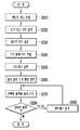
도 2는 본 발명의 실시예에 따른 비휘발성 메모리 장치의 소거 방법을 설명하기 위한 흐름도이다.2 is a flowchart illustrating an erase method of a nonvolatile memory device according to an exemplary embodiment of the present invention.
<도면의 주요 부분에 대한 부호의 설명><Explanation of symbols for the main parts of the drawings>
100 : 비휘발성 메모리 장치110 : 입력 버퍼100: nonvolatile memory device 110: input buffer
120 : 제어 로직 회로130 : 고전압 발생기120: control logic circuit 130: high voltage generator
140 : X-디코더150 : Y-디코더140: X-decoder 150: Y-decoder
160 : 데이터 입출력 회로PL1~PLM : 플레인160: data input / output circuit PL1 to PLM: plane
PB1~PBM : 페이지 버퍼MB1~MBn : 메모리 셀 블록PB1 to PBM: Page buffer MB1 to MBn: Memory cell block
본 발명은 비휘발성 메모리 장치 및 그 소거 방법에 관한 것으로, 특히 소거 동작 시간을 단축시킬 수 있는 비휘발성 메모리 장치 및 그 소거 방법에 관한 것이다.BACKGROUND OF THE INVENTION 1. Field of the Invention The present invention relates to a nonvolatile memory device and an erase method thereof, and more particularly, to a nonvolatile memory device and an erase method capable of shortening an erase operation time.
비휘발성 메모리 소자는 전원 공급이 중단되더라고 저장된 데이터가 지워지지 않는 메모리 소자이다. 이러한 비휘발성 메모리 소자 중에서 플래시 메모리 소자가 대표적인 비휘발성 메모리 소자에 해당된다. 플래시 메모리 소자는 프로그램 동작, 리드 동작 및 소거 동작을 통해 데이터를 저장하거나 출력한다. 여기서, 소거 동작은 저장된 데이터를 삭제하기 위하여 실시된다. 이러한 플래쉬 메모리 소자는 NOR형 플래시 메모리 소자의 NAND형 플래시 메모리 소자로 구분할 수 있으며, NAND형 플래시 메모리 소자의 소거 동작을 예로써 설명하면 다음과 같다.A nonvolatile memory device is a memory device in which stored data is not erased even when a power supply is interrupted. Among these nonvolatile memory devices, a flash memory device corresponds to a representative nonvolatile memory device. The flash memory device stores or outputs data through a program operation, a read operation, and an erase operation. Here, the erasing operation is performed to delete the stored data. Such a flash memory device may be classified into a NAND flash memory device of a NOR flash memory device, and an erase operation of the NAND flash memory device will be described as an example.
일반적으로, NAND형 플래시 메모리 소자의 셀 어레이는 싱글-플레인(single-plane) 타입과 멀티-플레인(multi-plane) 타입으로 나누어진다. 최근에는 집적도가 높아지고 메모리 용량이 증가함에 따라 멀티-플레인 타입의 플래시 메모리 소자가 증가하고 있다. 멀티-플레인 타입의 셀 어레이는 다수의 플레인으로 나누어지며, 각각의 플레인은 다수의 블록을 포함한다. 이러한 NAND형 플래시 메모리 소자의 소거 동작은 블록 단위로 이루어진다. 즉, 각각의 블록은 다수의 플래시 메모리 셀을 포함하며, 소거 동작 시 선택된 블록에 포함된 모든 메모리 셀의 데이터가 소거된다. 그런데, 플래시 메모리 소자에서는 프로그램 동작이나 소거 동작은 다른 메모리 소자들의 동작 속도에 비해 많은 시간이 요구된다. 따라서, 상대적으로 전체적 인 동작 속도가 느려지며, 다수의 블록을 소거할 경우 더 많은 동작 시간이 요구되어 동작 속도는 더욱 더 느려진다.In general, a cell array of a NAND type flash memory device is divided into a single-plane type and a multi-plane type. In recent years, as the degree of integration increases and memory capacity increases, multi-plane type flash memory devices are increasing. A multi-plane type cell array is divided into a number of planes, each plane containing a number of blocks. The erase operation of the NAND flash memory device is performed in units of blocks. That is, each block includes a plurality of flash memory cells, and data of all memory cells included in the selected block is erased during the erase operation. However, in a flash memory device, a program operation or an erase operation requires more time than an operation speed of other memory devices. Therefore, the overall operating speed becomes relatively slow, and when a large number of blocks are erased, more operating time is required, and thus the operating speed becomes slower.
이에 대하여, 본 발명이 제시하는 비휘발성 메모리 장치 및 그 소거 방법은 서로 다른 플레인에 포함되어 있어 플레인 어드레스는 상이하지만 블록 어드레스가 동일한 메모리 셀 블록들을 각각의 플레인에서 동시에 선택하여 소거 동작을 실시함으로써 소거 동작 시간을 단축시킬 수 있다.In contrast, the nonvolatile memory device and the erase method of the present invention are included in different planes so that the memory cell blocks having the same plane address but the same block address are erased by simultaneously selecting the memory cell blocks in each plane and performing the erase operation. The operation time can be shortened.
본 발명의 실시예에 따른 비휘발성 메모리 장치는 다수의 메모리 셀 블록을 각각 포함하는 플레인들과, 블록 어드레스를 포함하는 외부 어드레스 신호 및 소거 모드 비트 신호에 따라 각각 다른 플레인들에서 블록 어드레스가 동일한 메모리 셀 블록들 동시에 선택하기 위한 로우 어드레스 및 소거 명령 신호를 출력하는 제어 로직 회로와, 소거 명령 신호에 따라 소거 동작을 위한 소거 전압들을 발생시키는 고전압 발생기 및 소거 전압들을 로우 어드레스에 의해 선택된 메모리 셀 블록들로 인가하는 X-디코더를 포함한다.A nonvolatile memory device according to an embodiment of the present invention is a memory having the same block address in different planes according to planes each including a plurality of memory cell blocks, and an external address signal and an erase mode bit signal including a block address. A control logic circuit that outputs a row address and an erase command signal for simultaneously selecting the cell blocks, and memory cell blocks selected by the row address for a high voltage generator and erase voltages for generating erase voltages for an erase operation according to the erase command signal; It includes an X-decoder to apply.
상기에서, 제어 로직 회로는 소거 모드 비트 신호에 따라 선택된 플레인들 내에서 소거되어야할 메모리 셀 블록들 중 마지막 메모리 셀 블록의 소거 동작이 완료될 때까지 소거 동작이 완료되면 로우 어드레스 신호를 증가시킨다. 제어 로직 회로는 외부 어드레스 신호에 따라 컬럼 어드레스 신호를 더 출력한다. 상기의 불휘발성 메모리 장치는 컬럼 어드레스 신호에 따라 컬럼 디코더 신호를 출력하기 위한 Y-디코더, 및 플레인마다 각각 하나씩 대응하게 배치되는 페이지 버퍼들을 더 포함한다.In the above, the control logic circuit increases the row address signal when the erase operation is completed until the erase operation of the last memory cell block among the memory cell blocks to be erased in the planes selected according to the erase mode bit signal is completed. The control logic circuit further outputs a column address signal in accordance with an external address signal. The nonvolatile memory device further includes a Y-decoder for outputting a column decoder signal according to the column address signal, and page buffers corresponding to each plane.
본 발명의 실시예에 따른 비휘발성 메모리 장치의 소거 방법은 소거 대상 플레인 및 소거 대상 플레인에 포함된 메모리 셀 블록들 중 소거 대상 블록들을 결정하기 위한 소거 모드 비트 신호가 입력되는 단계와, 블록 어드레스를 포함하는 외부 어드레스가 입력되는 단계와, 소거 모드 비트 신호 및 블록 어드레스에 따라 소거 대상 플레인에 포함된 소거 대상 블록들 중 첫 번째 메모리 셀 블록들을 동시에 선택하기 위한 로우 어드레스 신호를 생성하는 단계와, 로우 어드레스 신호에 따라 선택된 메모리 셀 블록들의 소거 동작을 실시하는 단계, 및 소거 동작이 완료되면 로우 어드레스를 증가시키는 단계를 포함한다.An erase method of a nonvolatile memory device according to an embodiment of the present invention includes the steps of inputting an erase mode bit signal for determining erase target blocks among the erase target plane and the memory cell blocks included in the erase target plane; Generating a row address signal for simultaneously selecting first memory cell blocks among erased blocks included in an erased plane according to an erase mode bit signal and a block address; Performing an erase operation on the selected memory cell blocks according to the address signal, and increasing the row address when the erase operation is completed.
상기에서, 소거 모드 비트 신호가 입력되는 단계는, 플레인들 중 소거 대상 플레인을 결정하기 위한 플레인 선택 신호가 입력되는 단계와, 플레인의 분할 방식을 결정하기 위한 플레인 분할 신호가 입력되는 단계, 및 플레인에 포함된 메모리 셀 블록들 중 소거 대상 블록들을 선택하기 위한 블록 선택 신호가 입력되는 단계를 포함한다. 플레인 선택 신호, 플레인 분할 신호 및 블록 선택 신호가 각각 2비트 신호로 입력될 수 있다. 이 경우, 플레인 선택 신호가 '00'으로 입력되면 하나의 플레인만이 선택되고, '01'로 입력되면 이븐 플레인들이 선택되고, '10'으로 입 력되면 오드 플레인들이 선택되고, '11'로 입력되면 모든 플레인들이 선택된다. 플레인 분할 신호가 '01'로 입력되면 하나의 플레인에 포함된 모든 메모리 셀 블록들이 소거 대상 그룹으로 선택되고, '10'으로 입력되면 하나의 플레인이 2개의 메모리 셀 블록으로 나누어져 둘 중 하나의 그룹이 소거 대상 그룹으로 선택되고, '11'로 입력되면 하나의 플레인이 4개의 메모리 셀 블록으로 나누어져 4개의 그룹 중 하나의 그룹이 소거 대상 그룹으로 선택된다. 이때, 2개의 그룹 또는 4개의 그룹 중에서 블록 어드레스에 따라 하나의 그룹이 소거 대상 그룹으로 선택된다. 블록 선택 신호가 '00'으로 입력되면 하나의 메모리 셀 블록만이 소거 대상 블록으로 선택되고, '01'로 입력되면 이븐 메모리 셀 블록들이 소거 대상 블록들로 선택되고, '10'으로 입력되면 오드 메모리 셀 블록들이 소거 대상 블록들로 선택되고, '11'로 입력되면 모든 메모리 셀 블록들이 소거 대상 블록들로 선택된다. 로우 어드레스는 소거 동작이 종료될 때마다 소거 대상 블록들 중 마지막 메모리 셀 블록의 소거 동작이 완료될 때까지 증가된다.The step of inputting the erase mode bit signal may include inputting a plane selection signal for determining an erase target plane among the planes, inputting a plane division signal for determining a plane division method, and a plane And inputting a block select signal for selecting erase target blocks among the memory cell blocks included in the block. The plane select signal, the plane split signal, and the block select signal may be input as 2-bit signals, respectively. In this case, only one plane is selected when the plane select signal is inputted as '00', even planes are selected when inputted as '01', and odd planes are selected when inputted as '10', and '11' is selected. When entered, all planes are selected. When the plane split signal is input as '01', all memory cell blocks included in one plane are selected as an erasure target group, and when input as '10', one plane is divided into two memory cell blocks and one of the two When the group is selected as the erase target group and input as '11', one plane is divided into four memory cell blocks so that one of the four groups is selected as the erase target group. At this time, one group is selected as the erasing target group according to the block address from two groups or four groups. When the block selection signal is input as '00', only one memory cell block is selected as an erase target block, when it is input as '01', even memory cell blocks are selected as erase target blocks, and when it is input as '10', When the memory cell blocks are selected as the erase target blocks and input as '11', all the memory cell blocks are selected as the erase target blocks. Each time the erase operation is completed, the row address is increased until the erase operation of the last memory cell block among the erase target blocks is completed.
이하, 첨부된 도면을 참조하여 본 발명의 바람직한 실시예를 설명하기로 한다. 그러나, 본 발명은 이하에서 개시되는 실시예에 한정되는 것이 아니라 서로 다른 다양한 형태로 구현될 수 있으며, 본 발명의 범위가 다음에 상술하는 실시예에 한정되는 것은 아니다. 단지 본 실시예는 본 발명의 개시가 완전하도록 하며 통상의 지식을 가진 자에게 발명의 범주를 완전하게 알려주기 위해 제공되는 것이며, 본 발명의 범위는 본원의 특허 청구 범위에 의해서 이해되어야 한다.Hereinafter, with reference to the accompanying drawings will be described a preferred embodiment of the present invention. However, the present invention is not limited to the embodiments disclosed below, but may be implemented in various forms, and the scope of the present invention is not limited to the embodiments described below. Only this embodiment is provided to complete the disclosure of the present invention and to fully inform those skilled in the art, the scope of the present invention should be understood by the claims of the present application.
도 1은 본 발명의 실시예에 따른 비휘발성 메모리 장치의 블록도이다.1 is a block diagram of a nonvolatile memory device according to an embodiment of the present invention.
도 1을 참고하면, 비휘발성 메모리 장치(100)는 입력버퍼(110), 제어 로직 회로(120), 고전압 발생기(130), X-디코더(140), Y-디코더(150), 메모리 셀 어레이, 페이지 버퍼들(PB1 내지 PBM)(M은 정수) 및 데이터 입출력 회로(160)를 포함한다. 여기서, 메모리 셀 어레이는 복수의 플레인들(PL1 내지 PLM)(M은 정수)을 포함하며, 각각의 플레인은 복수의 메모리 셀 블록(MB1 내지 MBn)을 포함한다.Referring to FIG. 1, the
상기에서, 입력 버퍼(110)는 외부 어드레스 신호(ADD), 커맨드 신호(CMD) 또는 소거 모드 비트 신호(EM1 내지 EM3)를 수신하여 제어 로직 회로(120)에 출력한다.In the above, the
제어 로직 회로(120)는 칩 인에이블 신호(CEb)와 제어 신호들(REb, WEb, ALE, CLE)에 응답하여, 커맨드 신호(CMD), 외부 어드레스 신호(ADD) 또는 소거 모드 비트 신호(EM1 내지 EM3)를 수신한다. 이러한 제어 로직 회로(120)는 커맨드 신호(CMD)에 응답하여 프로그램 명령(PGM), 리드 명령(READ), 및 소거 명령(ERS) 중 하나를 발생한다. 또한, 제어 로직 회로(120)는 외부 어드레스 신호(ADD)에 따라 로우 어드레스 신호(RADD)와 컬럼 어드레스 신호(CADD)를 출력한다. 그 외에도, 본 발명의 제어 로직 회로(120)는 테스트 모드 신호가 커맨드 신호로 입력된 후 입력 버퍼(110)를 통해 소거 모드 비트 신호(EM1 내지 EM3)와 외부 어드레스 신호(ADD)가 입력되면, 소거 모드 비트 신호(EM1 내지 EM3)에 따라 플레인들(PL1 내지 PLM) 중 적어도 하나 이상의 플레인을 선택하고 선택된 플레인에 포함된 메모리 셀 블록들(MB1 내지 MBn) 중에서 외부 어드레스(ADD)에 포함된 블록 어드레스와 대응하는 메모리 셀 블록들이 동시에 선택되도록 로우 어드레스 신호(RADD)를 출력한다. 구체적인 동작은 도 2를 참조하여 후술하기로 한다.The
고전압 발생기(130)는 프로그램 명령(PGM), 리드 명령(READ) 및 소거 명령(ERS) 중 하나에 응답하여, 바이어스 전압들(VD, VS, VW1-VWK)(K는 정수)을 출력한다. 상기에서, 전압(VD)은 드레인 선택 라인(미도시)에 공급될 전압이고, 전압(VS)은 소스 선택 라인(미도시)에 공급될 전압이고, 전압(VW1 내지 VWK)은 워드 라인들(미도시)에 각각 공급될 전압들이다.The
X-디코더(140)는 로우 어드레스 신호(RADD)에 따라 플레인들(PL1 내지 PLM) 중 적어도 하나 이상의 플레인을 선택하고 선택된 플레인에 포함된 메모리 셀 블록들(MB1 내지 MBn) 중에서 외부 어드레스(ADD)에 포함된 블록 어드레스와 대응하는 메모리 셀 블록들에 고전압 발생기(130)의 바이어스 전압들(VD, VS, VW1 내지 VWK)을 동시에 공급한다. 구체적인 동작은 도 2를 참조하여 후술하기로 한다.The
Y-디코더(150)는 칼럼 어드레스 신호(CADD)를 디코딩하여 칼럼 디코딩 신호(CDEC)를 발생하고, 칼럼 디코딩 신호(CDEC)를 상기 페이지 버퍼들(PB1 내지 PBM)에 각각 출력한다.The Y-
페이지 버퍼들(PB1 내지 PBM)은 플레인들(PL1 내지 PLM)에 각각 하나씩 대응하게 배치된다. 페이지 버퍼들(PB1 내지 PBM) 각각은 데이터 입출력 회로(160)를 통해 입력되는 입력 데이터(Di1 내지 DiM 중 하나, M은 정수)를 래치하거나, 또는 칼럼 디코딩 신호(CDEC)에 응답하여 대응하는 플레인(PL1 내지 PLM 중 하나)의 비트 라인들(미도시) 중 일부 또는 전체를 선택하고, 그 선택된 비트 라인들로부터 수신되는 출력 데이터(Do1 내지 DoM 중 하나, M은 정수)를 래치한다.The page buffers PB1 to PBM are disposed corresponding to the planes PL1 to PLM, respectively. Each of the page buffers PB1 to PBM latches input data (one of Di1 to DiM, M is an integer) input through the data input /
상기에서 서술한 비휘발성 메모리 장치의 소거 방법을 설명하면 다음과 같다. 도 2는 본 발명의 실시예에 따른 비휘발성 메모리 장치의 소거 방법을 설명하기 위한 흐름도이다.The erasing method of the nonvolatile memory device described above will be described below. 2 is a flowchart illustrating an erase method of a nonvolatile memory device according to an exemplary embodiment of the present invention.
일반적으로 하나의 메모리 셀을 선택하기 위해서는 특정 플레인을 선택하기 위한 어드레스(이하, '플레인 어드레스'라 함), 특정 블록을 선택하기 위한 어드레스(이하, '블록 어드레스'라 함), 특정 워드라인을 선택하기 위한 어드레스(이하, '워드라인 선택 어드레스'라 함), 및 특정 비트라인을 선택하기 위한 어드레스(이하, '비트라인 선택 어드레스'라 함)가 필요하며, 외부 어드레스 신호(ADD)는 상기의 어드레스들을 포함한다. 여기서, 소거 동작은 블록 단위로 이루어지므로 플레인 어드레스와 블록 어드레스가 반드시 필요하다. 한편, 소거 동작은 하나의 블록에 대해서만 이루어지는데, 서로 다른 플레인에 포함된 블록들을 동시에 소거하기 위해서는 별도의 커맨드 신호가 입력되어야 한다. 예를 들어, 서로 다른 플레인에 포함된 블록들을 동시에 소거하는 경우, 입력 버퍼(110)를 통해 제어 로직 회로(120)로 테스트 모드 신호가 커맨드 신호로 입력되어 테스트 모드로 진입한다.(S210)In general, to select one memory cell, an address for selecting a specific plane (hereinafter referred to as a 'plane address'), an address for selecting a specific block (hereinafter referred to as a 'block address'), and a specific word line An address for selecting (hereinafter referred to as a 'word line selection address') and an address for selecting a specific bit line (hereinafter referred to as a 'bitline selection address') are required, and the external address signal ADD is Contains addresses. Since the erase operation is performed in units of blocks, a plane address and a block address are necessary. Meanwhile, the erase operation is performed for only one block. In order to simultaneously erase blocks included in different planes, a separate command signal must be input. For example, when simultaneously erasing blocks included in different planes, the test mode signal is input to the
이어서, 소거 모드 비트 신호(EM1 내지 EM3)가 입력된다. 소거 모드 비트 신호는 아래의 표 1 내지 표 3과 같은 플레인 선택 신호(EM1), 플레인 분할 신호(EM2) 및 블록 선택 신호(EM3)를 포함하며, 이들은 2비트의 신호로써 따로따로 입력된다.Subsequently, the erase mode bit signals EM1 to EM3 are input. The erase mode bit signal includes a plane select signal EM1, a plane split signal EM2, and a block select signal EM3 as shown in Tables 1 to 3 below, which are input separately as two-bit signals.
표 1을 참조하면, 먼저 플레인 선택 신호(EM1)가 입력되면, 플레인 선택 신호(EM1)에 따라 다수의 플레인들(PL1 내지 PLM) 중 어느 플레인들을 선택할 것인지 결정된다. 예를 들어, 플레인 선택 신호(EM1)가 '00'으로 입력되면, 이후에 입력될 외부 어드레스 신호(ADD)에 대응하는 하나의 플레인만이 선택된다. 플레인 선택 신호(EM1)가 '01'으로 입력되면, 이후에 입력될 외부 어드레스 신호(ADD)를 기준으로 이븐 플레인들이 선택된다. 플레인 선택 신호(EM1)가 '10'으로 입력되면, 이후에 입력될 외부 어드레스 신호(ADD)를 기준으로 오드 플레인들이 선택된다. 플레인 선택 신호(EM1)가 '11'로 입력되면, 모든 플레인들이 선택된다. 여기서, 선택된 플레인에는 소거 대상 블록이 포함되어 있는 것을 의미한다.Referring to Table 1, when the plane selection signal EM1 is input, it is determined which plane of the plurality of planes PL1 to PLM is selected according to the plane selection signal EM1. For example, when the plane selection signal EM1 is input as '00', only one plane corresponding to the external address signal ADD to be input later is selected. When the plane selection signal EM1 is input as '01', even planes are selected based on the external address signal ADD to be input later. When the plane selection signal EM1 is input as '10', the odd planes are selected based on the external address signal ADD to be input later. When the plane select signal EM1 is input as '11', all planes are selected. Here, the selected plane means that the erase target block is included.
표 2를 참조하면, 플레인 선택 신호(EM1)에 이어 플레인 분할 신호(EM2)가 입력되면, 선택된 플레인들을 어떻게 분할할 것인지 결정된다. 예를 들어, 플레인 분할 신호(EM2)가 '01'로 입력되면, 하나의 플레인에 포함된 모든 메모리 셀 블록들이 소거 대상 그룹으로 선택된다. 플레인 분할 신호(EM2)가 '10'으로 입력되면, 하나의 플레인이 2개의 메모리 셀 블록으로 나누어진다. 그리고, 이후에 입력될 외부 어드레스 신호(ADD)에 포함된 블록 어드레스에 따라 2개의 그룹 중 하나의 그룹이 소거 대상 그룹으로 선택된다. 플레인 분할 신호(EM2)가 '11'로 입력되면, 하나의 플레인이 4개의 메모리 셀 블록으로 나누어진다. 그리고, 이후에 입력될 외부 어드레스 신호(ADD)에 포함된 블록 어드레스에 따라 4개의 그룹 중 하나의 그룹이 소거 대상 그룹으로 선택된다.Referring to Table 2, when the plane division signal EM2 is input following the plane selection signal EM1, it is determined how to divide the selected planes. For example, when the plane split signal EM2 is input as '01', all memory cell blocks included in one plane are selected as an erase target group. When the plane split signal EM2 is input as '10', one plane is divided into two memory cell blocks. Then, one group of the two groups is selected as the erasing target group according to the block address included in the external address signal ADD to be input later. When the plane split signal EM2 is input as '11', one plane is divided into four memory cell blocks. Then, one group of four groups is selected as the erasing target group according to the block address included in the external address signal ADD to be input later.
표 3을 참조하면, 플레인 분할 신호(EM2)에 이어 블록 선택 신호(EM3)가 입력되면, 플레인 분할 신호(EM3)에 따라 선택된 그룹에 포함된 메모리 셀 블록들 중 어느 블록들을 선택할 것인지 결정된다. 예를 들어, 블록 선택 신호(EM3)가 '00'으로 입력되면, 이후에 입력될 외부 어드레스 신호(ADD)에 대응하는 하나의 메모리 셀 블록만이 선택된다. 블록 선택 신호(EM3)가 '01'로 입력되면, 플레인 분할 신호(EM3)에 따라 선택된 그룹 내에서 이후에 입력될 외부 어드레스 신호(ADD)를 기준으로 이븐 메모리 셀 블록들이 선택된다. 블록 선택 신호(EM3)가 '10'으로 입력되면, 플레인 분할 신호(EM3)에 따라 선택된 그룹 내에서 이후에 입력될 외부 어드레스 신호(ADD)를 기준으로 오드 메모리 블록들이 선택된다. 블록 선택 신호(EM3)가 '11'로 입력되면, 모든 메모리 블록들이 선택된다. 여기서, 선택된 플레인에는 소거 대상 블록이 포함되어 있는 것을 의미한다.Referring to Table 3, when the block select signal EM3 is input following the plane split signal EM2, it is determined which blocks of the memory cell blocks included in the selected group are selected according to the plane split signal EM3. For example, when the block select signal EM3 is input as '00', only one memory cell block corresponding to the external address signal ADD to be input later is selected. When the block select signal EM3 is input as '01', even memory cell blocks are selected based on the external address signal ADD to be input later in the group selected according to the plane split signal EM3. When the block select signal EM3 is input as '10', the odd memory blocks are selected based on the external address signal ADD to be input later in the group selected according to the plane split signal EM3. When the block select signal EM3 is input as '11', all memory blocks are selected. Here, the selected plane means that the erase target block is included.
상기에서는 레인 선택 신호(EM1), 플레인 분할 신호(EM2) 및 블록 선택 신호(EM3)가 모두 2비트로 입력되지만, 선택 방식이나 분할 방식을 보다 세분화하기 위해서 상기의 신호들이 2비트 이상의 신호로 입력될 수도 있다. 소거 모드 비트 신호(EM1 내지 EM3)는 제어 로직 회로(120) 내부에 포함된 저장 수단(예를 들어, 래치 회로)에 임시로 저장된다. 소거 모드 비트 신호(EM1 내지 EM3)의 입력이 완료되면, 테스트 모드의 종료를 알리는 신호가 커맨드 신호로 입력된다.(S230) 이어서, 소거 동작을 실시하기 위한 신호가 커맨드 신호로 입력되면 소거 동작 모드로 진입(S240)하며, 소거 대상 블록을 선택하기 위한 외부 어드레스 신호(ADD)가 입력(S250)되고, 멀티 블록 소거 명령이 커맨드 신호로 입력(S270)된다.In the above description, the lane selection signal EM1, the plane division signal EM2, and the block selection signal EM3 are all input in two bits, but in order to further refine the selection scheme or division scheme, the signals may be input as signals of two bits or more. It may be. The erase mode bit signals EM1 to EM3 are temporarily stored in storage means (eg, latch circuits) included in the
멀티 블록 소거 명령이 입력되면, 소거 모드 비트 신호(EM1 내지 EM3) 및 외부 어드레스 신호(ADD)에 따라 제어 로직 회로(120)가 출력된 소거 명령 신호(ERS), 로우 어드레스 신호(RADD) 및 컬럼 어드레스 신호(CADD)를 출력하고, 소거 동작이 진행된다.(S270) 보다 구체적으로 설명하면 다음과 같다.When the multi-block erase command is input, the
제어 로직 회로(120)는 소거 모드 비트 신호(EM1 내지 EM3)에 따라 플레인들(PL1 내지 PLM) 중 적어도 하나 이상의 플레인을 선택하고, 선택된 플레인에 포함된 메모리 셀 블록들(MB1 내지 MBn) 중에서 외부 어드레스(ADD)에 포함된 블록 어드레스와 대응하는 메모리 셀 블록들이 동시에 선택되도록 로우 어드레스 신호(RADD)를 출력한다. 예를 들어, 플레인 선택 신호(EM1)가 '10'으로 입력되고, 플레인 분할 신호(EM2)가 '01'로 입력되고, 블록 선택 신호(EM3)가 '01'로 입력되고, 블록 어드레스가 2번째 메모리 셀 블록(MB2)을 선택하는 신호로 입력되면, 제어 로직 회로(120)는 오드 플레인들(PLk; k는 홀수)에 포함된 모든 메모리 셀 블록들 중 2번째 메모리 셀 블록들(MB2)을 동시에 선택할 수 있도록 로우 어드레스 신호(RADD)를 출력한다. 그리고, 소거 명령 신호(ERS)에 따라 고전압 발생기(130)에서 소거 동작을 위한 전압들(VD, VD 및 VW1 내지 VWK)이 오드 플레인들(PLk; k는 홀수)에 포함된 2번째 메모리 셀 블록들(MB2)로 동시에 인가되어 소거 동작이 이루어진다.The
오드 플레인들(PLk; k는 홀수)에 포함된 2번째 메모리 셀 블록들(MB2)의 소거 동작이 완료되면, 소거 동작이 실시된 메모리 셀 블록이 마지막 셀 블록에 해당하는지를 판단한다.(S280) 구체적으로 설명하면, 블록 선택 신호(EM3)가 '01'로 입력되었으므로, 오드 플레인들(PLk; k는 홀수)에 포함된 모든 이븐 메모리 셀 블록들(MBj; j는 짝수)이 소거되어야 한다. 따라서, 소거 동작이 완료된 메모리 셀 블록(MB2)이 이븐 메모리 셀 블록들(MBj; j는 짝수) 중 마지막 메모리 셀 블록에 해당되는지를 판단한다.When the erase operation of the second memory cell blocks MB2 included in the odd planes PLk (k is an odd number) is completed, it is determined whether the erased memory cell block corresponds to the last cell block (S280). Specifically, since the block select signal EM3 is input as '01', all even memory cell blocks MBj (j is even) included in the odd planes PLk (k is odd) must be erased. Therefore, it is determined whether the memory cell block MB2 in which the erase operation is completed corresponds to the last memory cell block among the even memory cell blocks MBj (j is an even number).
메모리 셀 블록(MB2)은 이븐 메모리 셀 블록들(MBj; j는 짝수) 중 마지막 메모리 셀 블록이 아니므로, 제어 로직 회로(120)는 로우 어드레스 신호(RADD)를 증가시킨다.(S290) 구체적으로 설명하면, 블록 선택 신호(EM3)가 '01'로 입력되어 이븐 메모리 셀 블록들(MBj; j는 짝수)을 선택하므로 제어 로직 회로(120)는 오드 플레인들(PLk; k는 홀수)에 포함된 4번째 메모리 셀 블록들(MB4)이 선택되도록 로우 어드레스 신호(RADD)를 증가시킨다. 그리고, 증가된 로우 어드레스 신호(RADD)에 따라 오드 플레인들(PLk; k는 홀수)에 포함된 4번째 메모리 셀 블록들(MB4)의 소거 동작을 실시한다. 오드 플레인들(PLk; k는 홀수)에 포함된 이븐 메모리 블록들(MBj; j는 짝수) 중 마지막 이븐 메모리 셀 블록의 소거 동작이 완료될 때까지 상기의 단계들(S270 내지 S290)을 반복 실시한다.Since the memory cell block MB2 is not the last memory cell block among the even memory cell blocks MBj (j is an even number), the
상술한 바와 같이, 본 발명은 서로 다른 플레인에 포함되어 있어 플레인 어드레스는 상이하지만 블록 어드레스가 동일한 메모리 셀 블록들을 각각의 플레인에서 동시에 선택하여 소거 동작을 실시함으로써 소거 동작 시간을 단축시킬 수 있다. 또한, 플레인 선택 신호(EM1)로 소거 동작이 실시될 플레인을 선택하고 플레인 분할 신호(EM2) 및 블록 선택 신호(EM3)로 소거 동작이 실시될 메모리 셀 블록의 범위를 설정한 상태에서 소거 동작을 연속적으로 실시함으로써 소거 동작 시간을 보다 더 단축시킬 수 있다.As described above, the present invention is included in different planes so that the erase operation time can be shortened by simultaneously selecting the memory cell blocks having the same plane address but the same block address in each plane and performing the erase operation. In addition, an erase operation may be performed while selecting a plane to be erased with the plane selection signal EM1 and setting a range of a memory cell block to be erased with the plane division signal EM2 and the block selection signal EM3. By performing continuously, the erase operation time can be further shortened.
Claims (12)
Translated fromKoreanPriority Applications (2)
| Application Number | Priority Date | Filing Date | Title |
|---|---|---|---|
| KR1020060106429AKR100784007B1 (en) | 2006-10-31 | 2006-10-31 | Nonvolatile Memory Device and Erasing Method |
| US11/617,391US7623381B2 (en) | 2006-10-31 | 2006-12-28 | Non-volatile memory device and method of erasing the same |
Applications Claiming Priority (1)
| Application Number | Priority Date | Filing Date | Title |
|---|---|---|---|
| KR1020060106429AKR100784007B1 (en) | 2006-10-31 | 2006-10-31 | Nonvolatile Memory Device and Erasing Method |
Publications (1)
| Publication Number | Publication Date |
|---|---|
| KR100784007B1true KR100784007B1 (en) | 2007-12-10 |
Family
ID=39140392
Family Applications (1)
| Application Number | Title | Priority Date | Filing Date |
|---|---|---|---|
| KR1020060106429AActiveKR100784007B1 (en) | 2006-10-31 | 2006-10-31 | Nonvolatile Memory Device and Erasing Method |
Country Status (2)
| Country | Link |
|---|---|
| US (1) | US7623381B2 (en) |
| KR (1) | KR100784007B1 (en) |
Cited By (3)
| Publication number | Priority date | Publication date | Assignee | Title |
|---|---|---|---|---|
| US8427898B2 (en) | 2010-02-19 | 2013-04-23 | Samsung Electronics Co., Ltd. | Method and apparatus for performing multi-block access operation in nonvolatile memory device |
| KR101448169B1 (en)* | 2008-01-02 | 2014-10-13 | 삼성전자주식회사 | A three-dimensional memory device having a multi-plane structure |
| US9484104B2 (en) | 2014-03-04 | 2016-11-01 | Samsung Electronics Co., Ltd. | Nonvolatile memory system with block managing unit and method of operating the same |
Families Citing this family (2)
| Publication number | Priority date | Publication date | Assignee | Title |
|---|---|---|---|---|
| KR101085724B1 (en)* | 2010-05-10 | 2011-11-21 | 주식회사 하이닉스반도체 | Semiconductor memory device and operation method thereof |
| US8924777B2 (en)* | 2010-12-23 | 2014-12-30 | Samsung Electronics Co., Ltd. | Condensed FOTA backup |
Citations (1)
| Publication number | Priority date | Publication date | Assignee | Title |
|---|---|---|---|---|
| KR20050004142A (en)* | 2003-07-04 | 2005-01-12 | 가부시끼가이샤 도시바 | Semiconductor memory device and data writing device |
Family Cites Families (15)
| Publication number | Priority date | Publication date | Assignee | Title |
|---|---|---|---|---|
| US5798968A (en)* | 1996-09-24 | 1998-08-25 | Sandisk Corporation | Plane decode/virtual sector architecture |
| US6614685B2 (en)* | 2001-08-09 | 2003-09-02 | Multi Level Memory Technology | Flash memory array partitioning architectures |
| US6781878B2 (en)* | 2002-08-12 | 2004-08-24 | Matrix Semiconductor, Inc. | Dynamic sub-array group selection scheme |
| US6807119B2 (en)* | 2002-12-23 | 2004-10-19 | Matrix Semiconductor, Inc. | Array containing charge storage and dummy transistors and method of operating the array |
| JP2004241558A (en) | 2003-02-05 | 2004-08-26 | Toshiba Corp | Nonvolatile semiconductor memory device and manufacturing method thereof, semiconductor integrated circuit, and nonvolatile semiconductor memory device system |
| JP2004348788A (en)* | 2003-05-20 | 2004-12-09 | Sharp Corp | Semiconductor storage device and portable electronic device |
| US7012835B2 (en)* | 2003-10-03 | 2006-03-14 | Sandisk Corporation | Flash memory data correction and scrub techniques |
| US7173852B2 (en)* | 2003-10-03 | 2007-02-06 | Sandisk Corporation | Corrected data storage and handling methods |
| US6940759B2 (en)* | 2003-10-14 | 2005-09-06 | Atmel Corporation | Group erasing system for flash array with multiple sectors |
| US20050144516A1 (en)* | 2003-12-30 | 2005-06-30 | Gonzalez Carlos J. | Adaptive deterministic grouping of blocks into multi-block units |
| US8504798B2 (en)* | 2003-12-30 | 2013-08-06 | Sandisk Technologies Inc. | Management of non-volatile memory systems having large erase blocks |
| US7627712B2 (en)* | 2005-03-22 | 2009-12-01 | Sigmatel, Inc. | Method and system for managing multi-plane memory devices |
| KR100739256B1 (en)* | 2006-05-12 | 2007-07-12 | 주식회사 하이닉스반도체 | A flash memory device having a function of selectively changing a size of a memory cell block during an erase operation and an erase operation method thereof |
| US20080052446A1 (en)* | 2006-08-28 | 2008-02-28 | Sandisk Il Ltd. | Logical super block mapping for NAND flash memory |
| US7280398B1 (en)* | 2006-08-31 | 2007-10-09 | Micron Technology, Inc. | System and memory for sequential multi-plane page memory operations |
- 2006
- 2006-10-31KRKR1020060106429Apatent/KR100784007B1/enactiveActive
- 2006-12-28USUS11/617,391patent/US7623381B2/enactiveActive
Patent Citations (1)
| Publication number | Priority date | Publication date | Assignee | Title |
|---|---|---|---|---|
| KR20050004142A (en)* | 2003-07-04 | 2005-01-12 | 가부시끼가이샤 도시바 | Semiconductor memory device and data writing device |
Non-Patent Citations (1)
| Title |
|---|
| 10-2005-0004142, 10-2004-0074142 |
Cited By (4)
| Publication number | Priority date | Publication date | Assignee | Title |
|---|---|---|---|---|
| KR101448169B1 (en)* | 2008-01-02 | 2014-10-13 | 삼성전자주식회사 | A three-dimensional memory device having a multi-plane structure |
| US8427898B2 (en) | 2010-02-19 | 2013-04-23 | Samsung Electronics Co., Ltd. | Method and apparatus for performing multi-block access operation in nonvolatile memory device |
| US8593900B2 (en) | 2010-02-19 | 2013-11-26 | Samsung Electronics Co., Ltd. | Method and apparatus for performing multi-block access operation in nonvolatile memory device |
| US9484104B2 (en) | 2014-03-04 | 2016-11-01 | Samsung Electronics Co., Ltd. | Nonvolatile memory system with block managing unit and method of operating the same |
Also Published As
| Publication number | Publication date |
|---|---|
| US20080101119A1 (en) | 2008-05-01 |
| US7623381B2 (en) | 2009-11-24 |
Similar Documents
| Publication | Publication Date | Title |
|---|---|---|
| US8347042B2 (en) | Multi-plane type flash memory and methods of controlling program and read operations thereof | |
| US7760580B2 (en) | Flash memory device and erase method using the same | |
| KR20030011234A (en) | Memory devices with page buffer having dual registers and method of using the same | |
| CN101303890B (en) | Methods of reading data including comparing current and previous section addresses and related devices | |
| KR100784007B1 (en) | Nonvolatile Memory Device and Erasing Method | |
| JP2007012241A (en) | Method of controlling program operation in flash memory device | |
| CN100477007C (en) | Semiconductor memory device | |
| US8213235B2 (en) | Nonvolatile memory device | |
| US8634261B2 (en) | Semiconductor memory device and method of operating the same | |
| US7684254B2 (en) | Flash memory device and method of erasing memory cell block in the same | |
| JP6732710B2 (en) | Semiconductor memory device | |
| US8842474B2 (en) | Nonvolatile memory device and nonvolatile memory system including the same | |
| US10431312B2 (en) | Nonvolatile memory apparatus and refresh method thereof | |
| KR101138404B1 (en) | Memory system and method of operating thereof | |
| US9318198B2 (en) | Memory system and method of operating the same | |
| US20120106246A1 (en) | Non-volatile semiconductor memory device, method of writing the same, and semiconductor device | |
| US8687454B2 (en) | Semiconductor storage apparatus and semiconductor integrated circuit | |
| KR100908541B1 (en) | Copyback Program Method for Nonvolatile Memory Devices | |
| KR20080038936A (en) | Erasing Method of Nonvolatile Memory Device | |
| US6845040B2 (en) | Nonvolatile memory | |
| JP2007035163A (en) | Nonvolatile semiconductor memory device and signal processing system | |
| KR100300864B1 (en) | Programming device of nonvolatile memory | |
| KR100960447B1 (en) | Operation method of nonvolatile memory device | |
| KR20230105096A (en) | Page buffer and semiconductor apparatus including the same | |
| KR20240130483A (en) | Memory device for performing read operation and operating method thereof |
Legal Events
| Date | Code | Title | Description |
|---|---|---|---|
| A201 | Request for examination | ||
| PA0109 | Patent application | Patent event code:PA01091R01D Comment text:Patent Application Patent event date:20061031 | |
| PA0201 | Request for examination | ||
| E701 | Decision to grant or registration of patent right | ||
| PE0701 | Decision of registration | Patent event code:PE07011S01D Comment text:Decision to Grant Registration Patent event date:20071029 | |
| GRNT | Written decision to grant | ||
| PR0701 | Registration of establishment | Comment text:Registration of Establishment Patent event date:20071203 Patent event code:PR07011E01D | |
| PR1002 | Payment of registration fee | Payment date:20071203 End annual number:3 Start annual number:1 | |
| PG1601 | Publication of registration | ||
| PR1001 | Payment of annual fee | Payment date:20101125 Start annual number:4 End annual number:4 | |
| PR1001 | Payment of annual fee | Payment date:20111121 Start annual number:5 End annual number:5 | |
| FPAY | Annual fee payment | Payment date:20121121 Year of fee payment:6 | |
| PR1001 | Payment of annual fee | Payment date:20121121 Start annual number:6 End annual number:6 | |
| FPAY | Annual fee payment | Payment date:20131122 Year of fee payment:7 | |
| PR1001 | Payment of annual fee | Payment date:20131122 Start annual number:7 End annual number:7 | |
| FPAY | Annual fee payment | Payment date:20141126 Year of fee payment:8 | |
| PR1001 | Payment of annual fee | Payment date:20141126 Start annual number:8 End annual number:8 | |
| FPAY | Annual fee payment | Payment date:20151120 Year of fee payment:9 | |
| PR1001 | Payment of annual fee | Payment date:20151120 Start annual number:9 End annual number:9 | |
| FPAY | Annual fee payment | Payment date:20161125 Year of fee payment:10 | |
| PR1001 | Payment of annual fee | Payment date:20161125 Start annual number:10 End annual number:10 | |
| FPAY | Annual fee payment | Payment date:20171124 Year of fee payment:11 | |
| PR1001 | Payment of annual fee | Payment date:20171124 Start annual number:11 End annual number:11 | |
| FPAY | Annual fee payment | Payment date:20181126 Year of fee payment:12 | |
| PR1001 | Payment of annual fee | Payment date:20181126 Start annual number:12 End annual number:12 | |
| FPAY | Annual fee payment | Payment date:20191125 Year of fee payment:13 | |
| PR1001 | Payment of annual fee | Payment date:20191125 Start annual number:13 End annual number:13 | |
| PR1001 | Payment of annual fee | Payment date:20201124 Start annual number:14 End annual number:14 | |
| PR1001 | Payment of annual fee | Payment date:20221124 Start annual number:16 End annual number:16 | |
| PR1001 | Payment of annual fee | Payment date:20241126 Start annual number:18 End annual number:18 |