KR100782484B1 - Heat treatment equipment - Google Patents
Heat treatment equipmentDownload PDFInfo
- Publication number
- KR100782484B1 KR100782484B1KR1020060065611AKR20060065611AKR100782484B1KR 100782484 B1KR100782484 B1KR 100782484B1KR 1020060065611 AKR1020060065611 AKR 1020060065611AKR 20060065611 AKR20060065611 AKR 20060065611AKR 100782484 B1KR100782484 B1KR 100782484B1
- Authority
- KR
- South Korea
- Prior art keywords
- process tube
- regulating member
- pressure regulating
- gas
- tube
- Prior art date
- Legal status (The legal status is an assumption and is not a legal conclusion. Google has not performed a legal analysis and makes no representation as to the accuracy of the status listed.)
- Expired - Fee Related
Links
Images


Classifications
- H—ELECTRICITY
- H01—ELECTRIC ELEMENTS
- H01L—SEMICONDUCTOR DEVICES NOT COVERED BY CLASS H10
- H01L21/00—Processes or apparatus adapted for the manufacture or treatment of semiconductor or solid state devices or of parts thereof
- H01L21/02—Manufacture or treatment of semiconductor devices or of parts thereof
- H01L21/04—Manufacture or treatment of semiconductor devices or of parts thereof the devices having potential barriers, e.g. a PN junction, depletion layer or carrier concentration layer
- H01L21/18—Manufacture or treatment of semiconductor devices or of parts thereof the devices having potential barriers, e.g. a PN junction, depletion layer or carrier concentration layer the devices having semiconductor bodies comprising elements of Group IV of the Periodic Table or AIIIBV compounds with or without impurities, e.g. doping materials
- H01L21/30—Treatment of semiconductor bodies using processes or apparatus not provided for in groups H01L21/20 - H01L21/26
- H01L21/324—Thermal treatment for modifying the properties of semiconductor bodies, e.g. annealing, sintering
- F—MECHANICAL ENGINEERING; LIGHTING; HEATING; WEAPONS; BLASTING
- F27—FURNACES; KILNS; OVENS; RETORTS
- F27B—FURNACES, KILNS, OVENS OR RETORTS IN GENERAL; OPEN SINTERING OR LIKE APPARATUS
- F27B17/00—Furnaces of a kind not covered by any of groups F27B1/00 - F27B15/00
- F27B17/0016—Chamber type furnaces
- F27B17/0025—Chamber type furnaces specially adapted for treating semiconductor wafers
- H—ELECTRICITY
- H01—ELECTRIC ELEMENTS
- H01L—SEMICONDUCTOR DEVICES NOT COVERED BY CLASS H10
- H01L21/00—Processes or apparatus adapted for the manufacture or treatment of semiconductor or solid state devices or of parts thereof
- H01L21/67—Apparatus specially adapted for handling semiconductor or electric solid state devices during manufacture or treatment thereof; Apparatus specially adapted for handling wafers during manufacture or treatment of semiconductor or electric solid state devices or components ; Apparatus not specifically provided for elsewhere
- H01L21/67005—Apparatus not specifically provided for elsewhere
- H01L21/67011—Apparatus for manufacture or treatment
- H01L21/67098—Apparatus for thermal treatment
- H01L21/67109—Apparatus for thermal treatment mainly by convection
- H—ELECTRICITY
- H01—ELECTRIC ELEMENTS
- H01L—SEMICONDUCTOR DEVICES NOT COVERED BY CLASS H10
- H01L21/00—Processes or apparatus adapted for the manufacture or treatment of semiconductor or solid state devices or of parts thereof
- H01L21/67—Apparatus specially adapted for handling semiconductor or electric solid state devices during manufacture or treatment thereof; Apparatus specially adapted for handling wafers during manufacture or treatment of semiconductor or electric solid state devices or components ; Apparatus not specifically provided for elsewhere
- H01L21/67005—Apparatus not specifically provided for elsewhere
- H01L21/67242—Apparatus for monitoring, sorting or marking
- H01L21/67253—Process monitoring, e.g. flow or thickness monitoring
Landscapes
- Engineering & Computer Science (AREA)
- Physics & Mathematics (AREA)
- Condensed Matter Physics & Semiconductors (AREA)
- General Physics & Mathematics (AREA)
- Manufacturing & Machinery (AREA)
- Computer Hardware Design (AREA)
- Microelectronics & Electronic Packaging (AREA)
- Power Engineering (AREA)
- Mechanical Engineering (AREA)
- General Engineering & Computer Science (AREA)
Abstract
Translated fromKoreanDescription
Translated fromKorean도 1은 본 발명에 따른 열처리 설비의 일실시예를 도시한 단면도이다.1 is a cross-sectional view showing an embodiment of a heat treatment facility according to the present invention.
도 2는 도 1에 도시한 열처리 설비의 배기시 가스들의 유동 경로를 도시한 단면도이다.FIG. 2 is a cross-sectional view illustrating a flow path of gases when exhausting the heat treatment facility illustrated in FIG. 1.
도 3은 본 발명에 따른 열처리 설비의 다른 실시예를 도시한 단면도이다.3 is a cross-sectional view showing another embodiment of the heat treatment equipment according to the present invention.
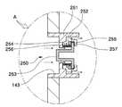
도 4는 도 3의 A 부분을 확대 도시한 절단면도이다.4 is an enlarged cross-sectional view of a portion A of FIG. 3.
도 5는 도 3의 체크 밸브가 소정거리 이동된 상태를 도시한 단면도이다.5 is a cross-sectional view illustrating a state in which the check valve of FIG. 3 is moved by a predetermined distance.
도 6은 본 발명에 따른 열처리 설비의 또다른 실시예를 도시한 단면도이다.Figure 6 is a cross-sectional view showing another embodiment of the heat treatment equipment according to the present invention.
본 발명은 반도체 제조 공정에 사용되는 설비에 관한 것으로, 특히, 열처리 공정을 통하여 웨이퍼와 같은 기판을 가공하는 열처리 설비에 관한 것이다.BACKGROUND OF THE
최근 들어 급속한 기술 개발이 진행되고 있는 반도체 제품은 단위 면적당 저장되는 데이터의 양 및 단위 시간당 데이터를 처리하는 처리 속도가 점차 빨라지도록 개발되고 있다.In recent years, semiconductor products, which have undergone rapid technological development, have been developed to increase the amount of data stored per unit area and the processing speed for processing data per unit time.
이러한 반도체 제품은 순수 실리콘 등으로 웨이퍼를 제조하는 웨이퍼 제조 공정, 제조된 웨이퍼 상에 반도체 칩들을 제조하는 팹(FAB) 공정, 제조된 반도체 칩들을 테스트 및 리페어하는 이디에스(EDS) 공정 및, 테스트 및 리페어된 반도체 칩들을 패키징하는 패키지 공정을 거쳐 제조된다.Such semiconductor products include a wafer manufacturing process for manufacturing a wafer from pure silicon, a Fab process for manufacturing semiconductor chips on the manufactured wafer, an EDS process for testing and repairing the manufactured semiconductor chips, and a test. And a package process for packaging the repaired semiconductor chips.
이와 같은 공정들 중 팹 공정은 웨이퍼 상에 실리콘 산화막을 형성하는 산화 공정, 웨이퍼 상에 감광제인 포토레지스트(photo-resist)를 도포하는 포토레지스트 도포 공정, 도포된 포토레지스트 상에 일정 회로패턴이 전사되도록 소정 파장의 광을 노광하는 노광 공정, 도포된 포토레지스트를 베이크하는 포토레지스트 베이크 공정, 웨이퍼 상에 노광된 패턴을 현상하는 현상 공정, 웨이퍼 상에 형성된 박막 중 일부 또는 전체를 식각하는 식각 공정, 웨이퍼 상에 소정 박막을 증착하는 증착 공정, 웨이퍼 상의 특정 막에 불순물을 주입하는 이온주입 공정, 이온주입된 불순물을 활성화시키는 어닐(anneal) 공정, 실리콘 내에 불순물을 확산시키는 확산 공정 등 다수의 단위 공정을 포함한다.Among these processes, the Fab process is an oxidation process for forming a silicon oxide film on a wafer, a photoresist coating process for applying a photoresist as a photoresist on the wafer, and a circuit pattern is transferred onto the applied photoresist. An exposure step of exposing light of a predetermined wavelength, a photoresist baking step of baking the applied photoresist, a developing step of developing an exposed pattern on the wafer, an etching step of etching part or all of the thin film formed on the wafer, Many unit processes such as a deposition process for depositing a predetermined thin film on a wafer, an ion implantation process for implanting impurities into a specific film on the wafer, an annealing process for activating ion implanted impurities, and a diffusion process for diffusing impurities into silicon. It includes.
그리고, 이디에스 공정은 웨이퍼 내 반도체 칩들을 테스트하여 양ㆍ불량을 선별하여 데이터를 발생시키는 프리-레이저(pre-laser) 공정, 발생된 데이터를 기준으로 레이저 빔을 이용하여 수선 가능한 반도체 칩들을 리페어하는 레이저 리페어(laser-repair) 공정, 웨이퍼 내 리페어한 반도체 칩들을 테스트하는 포스트-레이저 공정(post-laser), 웨이퍼의 뒷면을 연마하는 백-그라인딩(back grinding) 공정, 웨이퍼 내 반도체 칩들 상에 폴리이미드막(polyimide layer)과 같은 보호막을 도포하는 보호막 도포 공정 및, 도포된 폴리이미드막과 같은 보호막을 베이크하는 보호막 베이크 공정 등 다수의 단위공정을 포함한다.In addition, this process is a pre-laser process that generates semiconductor data by testing semiconductor chips in a wafer, and repairs semiconductor chips repairable using a laser beam based on the generated data. Laser repair process, post-laser test of repaired semiconductor chips in wafer, back grinding process to polish back side of wafer, semiconductor chips in wafer And a plurality of unit processes such as a protective film applying step of applying a protective film such as a polyimide layer, and a protective film baking step of baking a protective film such as the applied polyimide film.
이때, 이들 단위공정들 중 산화 공정, 포토레지스트 베이크 공정, 증착 공정, 어닐 공정, 확산 공정, 보호막 베이크 공정 등은 열처리 공정을 통하여 진행된다. 이러한, 열처리 공정을 수행하는 열처리 설비로는 매엽식과 배치식이 있으며, 배치식에는 수평로 설비와 종형로 설비가 있다. 통상, 반도체 제조 공정에서는 높은 생산성 및 공정의 신뢰성 등 여러가지 장점을 갖는 배치식의 종형로 설비가 많이 이용되고 있다.At this time, an oxidation process, a photoresist baking process, a deposition process, an annealing process, a diffusion process, a protective film baking process, and the like are performed through a heat treatment process. Heat treatment equipment for performing the heat treatment process, there is a single-leaf type and batch type, there is a horizontal type and vertical furnace equipment in the batch type. Usually, in the semiconductor manufacturing process, the batch type vertical furnace installation which has various advantages, such as high productivity and process reliability, is used a lot.
한편, 열처리 공정을 통하여 진행되는 단위공정들 중 보호막 베이크 공정은 반도체 칩에 형성된 각 패드들을 리드 프레임 등에 와이어 본딩한 다음 이를 에폭시 성형 화합물(epoxy molding compound) 등으로 둘러싸는 공정 즉, 패키지 공정 전에 진행되는 공정이다.Meanwhile, among the unit processes performed through the heat treatment process, the passivation layer baking process wire-bonds each pad formed on the semiconductor chip to a lead frame or the like, and then surrounds it with an epoxy molding compound or the like, before the package process. It is a process.
이러한 보호막 베이크 공정은 다수의 웨이퍼를 밀폐된 튜브 내부로 로딩한 다음 그 튜브를 약 250℃∼350℃ 정도의 고온에서 약 2시간 내지 3시간 정도로 가열함으로써 수행되고 있고, 이 공정이 진행되는 동안 튜브 내부로는 튜브 내부의 공정 분위기 형성을 위하여 공정가스인 N2 가스 등이 계속 공급되고 있다. 그리고, 이와 같은 보호막 베이크 공정시 튜브 내부에는 웨이퍼로부터 분출되는 실리콘 소스를 포함한 여러가지 좋지 않은 가스들이 발생될 수 있으므로, 베이크 공정이 진행되는 튜브는 크린룸 내부에 설치된 배기 덕트에 직접 연결되어 이러한 좋지 않은 가스들이 배기 덕트를 통해 계속 외부로 배출되도록 설치되어 있다.This protective film baking process is performed by loading a plurality of wafers into a sealed tube and then heating the tube at a high temperature of about 250 ° C to 350 ° C for about 2 hours to 3 hours. Inside, N2 gas, which is a process gas, is continuously supplied to form a process atmosphere inside the tube. In addition, various unfavorable gases, including a silicon source ejected from the wafer, may be generated in the tube during the protective film baking process, and thus, the tube in which the baking process is performed is directly connected to an exhaust duct installed in the clean room. Are installed to continue to be discharged to the outside through the exhaust duct.
하지만, 종래 보호막 베이크 공정의 경우, 베이크 공정이 진행되는 튜브가 배기 덕트에 직접 연결되어 있기 때문에, 공정이 진행되는 동안 튜브 내부의 가스 는 이 배기 덕트를 통해 빠르게 배출되어지게 된다. 그 결과, 공정이 진행되는 동안 튜브 내부의 압력은 열처리 설비가 설치된 크린룸 내부의 압력보다 낮은 압력(이하, '음압'이라 칭함)으로 계속 유지되어지게 된다.However, in the case of the conventional protective film baking process, since the tube undergoing the baking process is directly connected to the exhaust duct, the gas inside the tube is quickly discharged through the exhaust duct during the process. As a result, during the process, the pressure inside the tube is maintained at a pressure lower than the pressure inside the clean room where the heat treatment facility is installed (hereinafter referred to as 'negative pressure').
따라서, 이상과 같은 보호막 베이크 공정은 공정이 진행되는 동안 계속 튜브 내부의 압력이 음압으로 유지되어지기 때문에, 크린룸 내부에 존재하는 O2나 H2O 등의 옥시던트는 튜브 내부의 밀폐에도 불구하고 크린룸 내부의 압력과 튜브 내부의 압력차로 인하여 튜브 내부로 유입되어지게 된다. 그 결과, 튜브 내부로 유입된 옥시던트는 웨이퍼 베이크시 웨이퍼로부터 분출되는 실리콘 소스와 상호 반응하여 웨이퍼 상의 반도체 칩들에 형성된 각 패드들 상에 실리콘 산화막(SiO2)과 같은 이상 막질의 성장을 초래한다. 결과적으로, 각 패드들 상에 형성된 실리콘 산화막과 같은 이상 막질은 각 패드들과 리드 프레임 등을 연결하는 와이어 본딩을 저해하는 요소로 작용하여 패키징된 반도체 제품들의 작동 불능이나 성능 저하를 유발하게 된다.Therefore, since the protective film baking process as described above maintains the pressure inside the tube at a negative pressure during the process, the oxidants such as O2 and H2O present in the clean room have a pressure inside the clean room despite being sealed inside the tube. Due to the pressure difference between the inside and the tube is introduced into the tube. As a result, the oxidant introduced into the tube reacts with the silicon source ejected from the wafer at the time of baking, resulting in the growth of an abnormal film such as a silicon oxide film (SiO 2) on each of the pads formed in the semiconductor chips on the wafer. As a result, abnormal film quality such as silicon oxide film formed on each pad acts as a factor that inhibits wire bonding between the pads and the lead frame, resulting in inoperability or deterioration of the packaged semiconductor products.
본 발명이 이루고자 하는 기술적 과제는 웨이퍼 상의 반도체 칩들에 형성된 각 패드들 상에 이상 막질이 성장하는 것을 미연에 방지할 수 있는 열처리 설비를 제공하는데 있다.SUMMARY OF THE INVENTION The present invention has been made in an effort to provide a heat treatment facility that can prevent an abnormal film quality from growing on each pad formed on semiconductor chips on a wafer.
본 발명이 이루고자 하는 다른 기술적 과제는 크린룸 내부에 존재하는 옥시던트가 공정이 진행되는 튜브 내부로 유입되는 것을 미연에 방지할 수 있는 열처리 설비를 제공하는데 있다.Another technical problem to be achieved by the present invention is to provide a heat treatment facility that can prevent the oxidant existing in the clean room from flowing into the inner tube.
본 발명의 제 1관점에 따르면, 프로세스 튜브와, 상기 프로세스 튜브에 연결되어 상기 프로세스 튜브 내부의 가스들을 배기하는 배기 덕트 및, 상기 프로세스 튜브와 상기 배기 덕트의 사이에 개재되되, 상기 프로세스 튜브와 상기 배기 덕트에 각각 연통되고 하나 또는 다수개의 개구(opening)를 갖는 중공의 압력조절부재를 포함하는 열처리 설비가 제공된다.According to a first aspect of the present invention, a process tube, an exhaust duct connected to the process tube to exhaust gases in the process tube, and interposed between the process tube and the exhaust duct, the process tube and the A heat treatment facility is provided that includes a hollow pressure regulating member that is in communication with the exhaust duct and has one or a plurality of openings, respectively.
다른 실시예에 있어서, 상기 개구에는 상기 압력조절부재 내부의 가스가 상기 개구를 통해 외부로 배출되는 것을 차단하는 체크 밸브가 설치될 수 있다.In another embodiment, the opening may be provided with a check valve for blocking the gas inside the pressure regulating member to be discharged to the outside through the opening.
또다른 실시예에 있어서, 상기 프로세스 튜브의 일면에는 상기 프로세스 튜브 내부의 가스들이 배기되는 가스배기홀이 형성될 수 있다. 이 경우, 상기 압력조절부재는 상기 가스배기홀에 연통되도록 상기 프로세스 튜브의 일면에 접하게 설치될 수 있다.In another embodiment, a gas exhaust hole through which gases in the process tube are exhausted may be formed on one surface of the process tube. In this case, the pressure regulating member may be installed in contact with one surface of the process tube so as to communicate with the gas exhaust hole.
또다른 실시예에 있어서, 상기 가스배기홀은 상기 프로세스 튜브의 상면에 형성될 수 있다. 이 경우, 상기 압력조절부재는 상기 프로세스 튜브의 상면에 접하게 설치될 수 있다.In another embodiment, the gas exhaust hole may be formed on the upper surface of the process tube. In this case, the pressure regulating member may be installed in contact with the upper surface of the process tube.
또다른 실시예에 있어서, 상기 가스배기홀은 상기 프로세스 튜브의 측면에 형성될 수 있다. 이 경우, 상기 압력조절부재는 상기 프로세스 튜브의 측면에 접하게 설치될 수 있다.In another embodiment, the gas exhaust hole may be formed on the side of the process tube. In this case, the pressure regulating member may be installed in contact with the side of the process tube.
또다른 실시예에 있어서, 상기 프로세스 튜브는 상기 압력조절부재의 하부에 연통될 수 있고, 상기 배기 덕트는 상기 압력조절부재의 상부에 연통될 수 있다. 이 경우, 상기 압력조절부재는 원통 형상으로 형성될 수 있고, 상기 개구는 상기 압력조절부재의 측면에 형성될 수 있다.In another embodiment, the process tube may be in communication with the bottom of the pressure regulating member, the exhaust duct may be in communication with the top of the pressure regulating member. In this case, the pressure regulating member may be formed in a cylindrical shape, and the opening may be formed on the side of the pressure regulating member.
또다른 실시예에 있어서, 상기 열처리 설비는 상기 프로세스 튜브의 외측에 배치되어 상기 프로세스 튜브를 가열하는 히터를 더 포함할 수 있다.In another embodiment, the heat treatment facility may further include a heater disposed outside the process tube to heat the process tube.
본 발명의 제 2관점에 따르면, 프로세스 튜브와, 상기 프로세스 튜브 내부의 가스들을 배기하는 배기 덕트와, 상기 프로세스 튜브와 상기 배기 덕트의 사이에 개재되며 하나 또는 다수개의 개구를 갖는 중공의 압력조절부재와, 상기 프로세스 튜브와 상기 압력조절부재를 상호 연통시키는 제1가스배기라인 및, 상기 압력조절부재와 상기 배기 덕트를 상호 연통시키는 제2가스배기라인을 포함하는 열처리 설비가 제공된다.According to a second aspect of the present invention, a hollow pressure regulating member having a process tube, an exhaust duct for exhausting gases in the process tube, and one or a plurality of openings interposed between the process tube and the exhaust duct. And a first gas exhaust line for communicating the process tube and the pressure regulating member with each other, and a second gas exhaust line for communicating the pressure regulating member and the exhaust duct with each other.
다른 실시예에 있어서, 상기 개구에는 상기 압력조절부재 내부의 가스가 상기 개구를 통해 외부로 배출되는 것을 차단하는 체크 밸브가 설치될 수 있다.In another embodiment, the opening may be provided with a check valve for blocking the gas inside the pressure regulating member to be discharged to the outside through the opening.
또다른 실시예에 있어서, 상기 제1가스배기라인의 일측단은 상기 프로세스 튜브의 상면에 연결될 수 있고, 상기 제1가스배기라인의 타측단은 상기 압력조절부재의 하면에 연결될 수 있다.In another embodiment, one end of the first gas exhaust line may be connected to an upper surface of the process tube, and the other end of the first gas exhaust line may be connected to a lower surface of the pressure regulating member.
또다른 실시예에 있어서, 상기 제2가스배기라인의 일측단은 상기 압력조절부재의 상면에 연결될 수 있고, 상기 제2가스배기라인의 타측단은 상기 배기 덕트의 하면에 연결될 수 있다.In another embodiment, one end of the second gas exhaust line may be connected to an upper surface of the pressure regulating member, and the other end of the second gas exhaust line may be connected to a lower surface of the exhaust duct.
또다른 실시예에 있어서, 상기 압력조절부재는 원통 형상으로 형성될 수 있다. 이 경우, 상기 개구는 상기 압력조절부재의 측면에 형성될 수 있다.In another embodiment, the pressure regulating member may be formed in a cylindrical shape. In this case, the opening may be formed on the side of the pressure regulating member.
또다른 실시예에 있어서, 상기 열처리 설비는 상기 프로세스 튜브의 외측에 배치되어 상기 프로세스 튜브를 가열하는 히터를 더 포함할 수 있다.In another embodiment, the heat treatment facility may further include a heater disposed outside the process tube to heat the process tube.
이하, 첨부한 도면들을 참조하여 본 발명의 바람직한 실시예들을 상세히 설명하기로 한다. 그러나, 본 발명은 여기서 설명되어지는 실시예들에 한정되지 않고 다른 형태로 구체화될 수도 있다. 오히려, 여기서 소개되는 실시예들은 개시된 내용이 철저하고 완전해질 수 있도록 그리고 당업자에게 본 발명의 사상이 충분히 전달될 수 있도록 하기 위해 제공되어지는 것이다. 명세서 전체에 걸쳐서 동일한 참조번호들은 동일한 구성요소들을 나타낸다.Hereinafter, exemplary embodiments of the present invention will be described in detail with reference to the accompanying drawings. However, the present invention is not limited to the embodiments described herein and may be embodied in other forms. Rather, the embodiments introduced herein are provided to ensure that the disclosed subject matter is thorough and complete, and that the scope of the invention to those skilled in the art will fully convey. Like numbers refer to like elements throughout.
도 1은 본 발명에 따른 열처리 설비의 일실시예를 도시한 단면도이고, 도 2는 도 1에 도시한 열처리 설비의 배기시 가스들의 유동 경로를 도시한 단면도이다.1 is a cross-sectional view showing an embodiment of a heat treatment facility according to the present invention, Figure 2 is a cross-sectional view showing a flow path of the gases during the exhaust of the heat treatment facility shown in FIG.
도 1과 도 2를 참조하면, 본 발명의 일실시예에 따른 열처리 설비(100)는 수직형 프로세스 튜브(110)를 구비한 종형로 설비로 크린룸(180) 내부에 설치된다.1 and 2, a
구체적으로, 본 발명의 일실시예에 따른 열처리 설비(100)는 웨이퍼(90)에 열처리 공정을 수행하기 위한 공간을 제공하며 일측에 그 내부로의 웨이퍼 입출을 위한 웨이퍼 입출구가 마련된 프로세스 튜브(110), 상기 프로세스 튜브(110)의 웨이퍼 입출구를 밀폐하는 튜브 캡(150), 공정 진행에 따라 상기 튜브 캡(150)을 이동시키는 이동유닛(160), 상기 프로세스 튜브(110)를 가열하는 히터(120), 상기 프로세스 튜브(110) 내부의 가스들을 외부로 배기하는 배기 덕트(185), 상기 프로세 스 튜브(110)와 상기 배기 덕트(185)의 사이에 개재되며 공정 진행시 상기 프로세스 튜브(110) 내부의 압력(P1)이 상기 프로세스 튜브(110) 외부의 압력인 크린룸(180) 내부의 압력(P2)보다 더 높게 유지되도록 하는 압력조절부재(140) 및, 상기 열처리 설비(100)의 구동을 전반적으로 제어하는 제어유닛(미도시)을 포함한다.Specifically, the
상기 프로세스 튜브(110)는 그 내부로 다수의 웨이퍼(90)가 유입될 수 있는 중공의 원통 형상으로 형성되며, 열처리 공정에 적합한 석영 재질로 이루어진다. 그리고, 웨이퍼(90)의 입출을 위한 상기 웨이퍼 입출구는 상기 프로세스 튜브(110)의 하부에 마련된다. 따라서, 다수의 웨이퍼(90)는 상기 다수의 웨이퍼(90)를 수직 방향으로 정렬 가능하게 하는 웨이퍼 보트(170)에 순차적으로 적재된 다음, 상기 웨이퍼 입출구를 통해 상기 프로세스 튜브(110)의 내부로 유입된다. 그리고, 상기 프로세스 튜브(110)의 상측에는 상기 프로세스 튜브(110) 내부의 가스들이 배기되도록 가스배기홀(118)이 형성된다. 상기 가스배기홀(118)은 별도의 라인인 제1가스배기라인(183)을 통해 상기 압력조절부재(140)에 연통될 수도 있고, 상기 압력조절부재(140)에 직접 연통될 수도 있다.The
또한, 상기 프로세스 튜브(110)의 하부에는 상기 프로세스 튜브(110)에 접촉되어 상기 프로세스 튜브(110)를 밀착 지지하는 플랜지(112)가 설치될 수 있다. 이 경우, 상기 플랜지(112)의 하부에도 웨이퍼(90)의 입출을 위한 웨이퍼 입출구가 형성될 수 있으며, 상기 웨이퍼 보트(170)는 상기 플랜지(112)에 형성된 웨이퍼 입출구를 통해 상기 프로세스 튜브(110) 내부로 유입된다. 또, 상기 플랜지(112)의 일측에는 열처리 공정이 진행되는 동안 상기 프로세스 튜브(110) 내부로 소정 분위기 가스를 공급하는 가스공급라인(114)이 설치된다. 이때, 소정 분위기 가스는 N2 가스일 수 있다. 한편, 상기 가스공급라인(114)은 상기 플랜지(112)의 일측 이외에도 상기 프로세스 튜브(110)의 일측에 직접 설치되어 상기 프로세스 튜브(110) 내부로 소정 분위기 가스를 공급할 수 있다.In addition, a
상기 튜브 캡(150)은 상기 이동유닛(160)에 의해 이동되어 상기 프로세스 튜브(110)의 웨이퍼 입출구를 선택적으로 밀폐하는 역할을 한다. 따라서, 상기 프로세스 튜브(110)는 상기 튜브 캡(150)으로 인하여 외부로부터 밀폐된다. 이때, 상기 프로세스 튜브(110)에 접촉되는 상기 튜브 캡(150)의 상부에는 밀폐링(155)이 구비될 수 있다. 이 경우, 상기 프로세스 튜브(110)와 상기 튜브 캡(150) 사이의 리크(leak)는 최소화될 수 있다. 한편, 상기 프로세스 튜브(110)의 하부에 상기 프로세스 튜브(110)를 밀착 지지하는 플랜지(112)가 설치될 경우, 상기 튜브 캡(150)은 상기 플랜지(112)에 형성된 웨이퍼 입출구를 밀폐함으로써, 상기 프로세스 튜브(110)를 밀폐하게 된다.The
상기 이동유닛(160)은 열처리 공정의 진행에 따라 상기 튜브 캡(150)이 상기 프로세스 튜브(110)를 밀폐하도록 상기 튜브 캡(150)을 이동시키는 역할을 한다. 따라서, 상기 이동유닛(160)은 상기 제어유닛의 제어에 따라 상기 튜브 캡(150)을 소정거리 이동시킬 수 있는 구성이면 다양한 구성이 적용가능하다. 예를 들면, 상기 이동유닛(160)은 볼스크류 방식이나 실린더 방식 또는 리니어 모터 방식 등이 적용될 수 있다.The moving
일실시예로, 상기 이동유닛(160)은 상기 튜브 캡(150)을 지지하는 캡 베이 스(161)와, 상기 프로세스 튜브(110)의 하부에 상하 방향으로 설치되되 그 외주면에 수나사가 형성된 구동축(168)과, 상기 구동축(168)이 회전되도록 상기 구동축(168)의 하부와 상부에 각각 설치되는 베어링들(165,166)과, 상기 구동축(168)의 회전 방향에 따라 상하 방향으로 이동되도록 상기 구동축(168)에 설치되며 그 일측이 상기 캡 베이스(161)에 연결된 베이스 연결체(163)와, 상기 베이스 연결체(163)가 상하 방향으로 이동되도록 소정 속도로 정역회전되는 모터(167) 및, 상기 모터(167)의 회전에 의해 상기 구동축(168)이 회전되도록 상기 모터(167)의 회전력을 상기 구동축(168)으로 전달하는 동력전달체(164)를 포함한다.In one embodiment, the moving
따라서, 상기 튜브 캡(150)의 이동이 필요하게 되면, 상기 제어유닛은 상기 모터(167)에 소정 시그날을 전송하여 상기 모터(167)를 회전시키게 된다. 이에, 상기 구동축(168)은 상기 동력전달체(164)의 동력 전달로 인하여 소정 속도로 회전되어지고, 상기 베이스 연결체(163)는 상기 구동축(168)의 회전에 따라 소정거리 상하 이동된다. 그 결과, 상기 캡 베이스(161)는 상기 베이스 연결체(163)의 이동에 따라 소정거리 상하 이동되고, 상기 캡 베이스(161)의 상부에 위치된 상기 튜브 캡(150)도 상기 캡 베이스(161)의 상하 이동에 따라 소정거리 상하 이동된다. 결과적으로, 상기 프로세스 튜브(110)는 상기 튜브 캡(150)의 이동에 의해 개폐된다.Therefore, when the
한편, 상기 이동유닛(160)은 상기 튜브 캡(150)과 상기 캡 베이스(161)의 사이에 설치되는 탄성부재(162)를 더 포함할 수 있다. 이 경우, 상기 튜브 캡(150)을 지지하는 상기 캡 베이스(161)의 지지력은 상기 탄성부재(162)에 의해 완충될 수 있다. 따라서, 상기 튜브 캡(150)이 상기 프로세스 튜브(110)를 밀폐할 시 상기 튜 브 캡(150)은 상기 탄성부재(162)의 탄성력에 의하여 상기 프로세스 튜브(110)에 부드럽게 접촉될 수 있게 되고, 상기 프로세스 튜브(110)를 강하게 밀폐시킬 수 있게 된다.Meanwhile, the
상기 히터(120)는 상기 프로세스 튜브(110)의 외측에 배치되어 상기 프로세스 튜브(110)를 가열한다. 이때, 상기 히터(120)는 상기 프로세스 튜브(110)의 내부에서 진행되는 각 열처리 공정에 따라 상기 프로세스 튜브(110)를 각각 다른 온도로 가열할 수 있다. 일 예로, 상기 프로세스 튜브(110) 내부에서 진행되는 열처리 공정이 확산 공정일 경우, 상기 히터(120)는 상기 프로세스 튜브(110)의 내부 온도가 약 800∼1200℃가 되도록 가열할 수 있고, 상기 프로세스 튜브(110) 내부에서 진행되는 열처리 공정이 증착 공정일 경우, 상기 히터(120)는 상기 프로세스 튜브(110)의 내부 온도가 약 500∼1000℃가 되도록 가열할 수 있다. 다른 예로, 상기 프로세스 튜브(110) 내부에서 진행되는 공정이 웨이퍼 내 반도체 칩들 상에 도포된 폴리이미드막과 같은 보호막을 베이크하는 공정 즉, 보호막 베이크 공정일 경우, 상기 히터(120)는 상기 프로세스 튜브(110)의 내부 온도가 약 250∼350℃가 되도록 가열할 수 있다.The
그리고, 상기 히터(120)는 상기 프로세스 튜브(110)를 가열할 수 있는 방식이면, 여러가지 다양한 방식이 모두 적용가능하다. 예를 들면, 상기 히터(120)는 코일 가열방식이나 램프 가열방식 또는 펠티어 소자 등을 이용한 방식이 적용가능하다. 바람직하게, 상기 히터(120)는 코일 가열방식일 수 있다. 한편, 상기 히터(120)의 외측에는 상기 히터(120)를 둘러싸는 프로세스 챔버(130)가 더 설치될 수 있다. 이 경우, 상기 프로세스 튜브(110)를 가열하는 상기 히터(120)의 열은 상기 히터(120)를 둘러싸는 상기 프로세스 챔버(130)로 인하여 외부로 유출되지 않기 때문에, 상기 히터(120)의 가열 효율은 극대화된다.In addition, as long as the
상기 배기 덕트(185)는 상기 프로세스 챔버(130)의 상부에 설치되며, 상기 압력조절부재(140)를 매개로 상기 프로세스 튜브(110)에 연결된다. 따라서, 상기 프로세스 챔버(130) 내부의 가스들은 상기 압력조절부재(140)와 상기 배기 덕트(185)를 통하여 외부로 배출된다. 구체적으로, 상기 배기 덕트(185)의 일측은 상기 압력조절부재(140)에 연결되며, 상기 배기 덕트(185)의 타측은 가스펌핑장치(미도시)에 연결된다. 따라서, 상기 프로세스 튜브(110) 내 가스들은 상기 가스펌핑장치의 작동에 의해 상기 압력조절부재(140)와 상기 배기 덕트(185)를 통하여 외부로 배출된다. 여기서, 상기 배기 덕트(185)의 일측은 상기 압력조절부재(140)에 직접 연결될 수도 있고, 별도의 라인인 제2가스배기라인(187)을 통하여 상기 압력조절부재(140)에 연결될 수도 있다.The
상기 압력조절부재(140)는 열처리 공정의 진행시 상기 프로세스 튜브(110) 내부의 압력이 상기 열처리 설비(100)가 설치된 크린룸(180) 내부의 압력보다 더 높게 유지되도록 하는 역할을 하며, 상기 프로세스 튜브(110)와 상기 배기 덕트(185)의 사이에 개재된다. 일실시예로, 상기 압력조절부재(140)의 하부는 전술한 제1가스배기라인(183)을 매개로 상기 프로세스 튜브(110)의 상부에 연결될 수 있고, 상기 압력조절부재(140)의 상부는 전술한 제2가스배기라인(187)을 매개로 상기 배기 덕트(185)의 하부에 연결될 수 있다. 하지만, 다른 실시예로, 상기 압력조절 부재(140)의 하부와 상부는 각각 상기 프로세스 튜브(110)와 상기 배기 덕트(185)에 직접 연결될 수도 있다. 이 경우, 상기 압력조절부재(140)의 하부는 전술한 바와 같이, 상기 프로세스 튜브(110) 내부의 가스들이 배기되도록 마련된 상기 가스배기홀(118)에 연통되도록 설치됨이 바람직하다. 이때, 상기 압력조절부재(140)는 상기 프로세스 튜브(110)에 직접 연결된 후드일 수 있다.The
구체적으로, 상기 압력조절부재(140)는 중공의 원통 형상으로 형성될 수 있다. 따라서, 상기 프로세스 튜브(110)에 연결된 제1가스배기라인(183)은 원통 형상인 상기 압력조절부재(140)의 하면에 연결될 수 있고, 상기 배기 덕트(185)에 연결된 제2가스배기라인(187)은 원통 형상인 상기 압력조절부재(140)의 상면에 연결될 수 있다.Specifically, the
그리고, 상기 압력조절부재(140)에는 상기 크린룸(180)과 연통되는 하나 또는 다수개의 개구(opening,143)가 형성된다. 따라서, 상기 배기 덕트(185)와 상기 배기 덕트(185)에 연결된 상기 압력조절부재(140)를 이용하여 상기 프로세스 튜브(110) 내부의 가스를 배기할 시 상기 개구(143)로는 상기 프로세스 튜브(110) 외부의 가스 즉, 상기 크린룸(180) 내부의 가스가 유입될 수 있다. 다시 말하면, 상기 배기 덕트(185)와 상기 배기 덕트(185)에 연결된 상기 압력조절부재(140)를 이용하여 상기 프로세스 튜브(110) 내부의 가스를 배기할 시 상기 개구(143)로 인하여 상기 프로세스 튜브(110) 내부의 가스 뿐만 아니라 상기 프로세스 튜브(110) 외부의 가스도 같이 상기 압력조절부재(140)의 내부로 유입되어 상기 배기 덕트(185)로 배출될 수 있다. 여기서, 상기 개구(143)는 상기 압력조절부재(140)의 측면에 형성될 수 있다.The
한편, 본 발명에 따른 열처리 설비는 도 3 내지 도 5에 도시된 바와 같이 다른 실시예로도 구현될 수 있다.On the other hand, the heat treatment equipment according to the present invention may be implemented in other embodiments as shown in Figures 3 to 5.
도 3은 본 발명에 따른 열처리 설비의 다른 실시예를 도시한 단면도이고, 도 4는 도 3의 A 부분을 확대 도시한 절단면도이며, 도 5는 도 3의 체크 밸브가 소정거리 이동된 상태를 도시한 단면도이다.Figure 3 is a cross-sectional view showing another embodiment of the heat treatment equipment according to the present invention, Figure 4 is an enlarged cross-sectional view showing a portion A of Figure 3, Figure 5 is a state in which the check valve of Figure 3 is moved a predetermined distance It is sectional drawing.
도 3 내지 도 5를 참조하면, 본 발명에 따른 다른 실시예인 열처리 설비(200)는 일실시예에서 설명한 열처리 설비(100)의 구성 외에 체크 밸브(250)를 더 포함한다. 상기 체크 밸브(250)는 상기 압력조절부재(140)에 형성된 상기 개구(143)에 설치되며, 상기 압력조절부재(140) 내부의 가스가 상기 개구(143)를 통해 상기 크린룸(180) 측으로 배출되는 것을 차단하는 역할을 한다. 상기 체크 밸브(250)는 상기 배기 덕트(185)를 통해 상기 압력조절부재(140) 내부의 가스가 원활하게 잘 배기될 때에만 개방되고 그렇지 않을 경우에는 밀폐되는 밸브 즉, 노말 오픈 밸브(Normal open valve)일 수 있다.3 to 5, the
구체적으로, 상기 체크 밸브(250)는 상기 개구(143)에 설치되며 내부에 가스유입경로(252)가 형성된 밸브 하우징(251)과, 상기 밸브 하우징(251)의 내부에 설치되며 소정거리 왕복 이동되면서 상기 가스유입경로(252)를 개폐하는 이동부재(253) 및, 상기 밸브 하우징(251)과 상기 이동부재(253)의 사이에 설치되며 상기 가스유입경로(252)가 상기 압력조절부재(140) 내부의 가스가 원활하게 잘 배기될 때에만 오픈되도록 하는 탄성부재(254)를 포함한다.In detail, the
이때, 상기 밸브 하우징(251)은 튜브 형상으로 형성될 수 있다. 그리고, 상기 밸브 하우징(251)의 내부에는 한쌍의 제1걸림돌기(256)와 제2걸림돌기(257)가 상기 밸브 하우징(251)의 길이방향으로 소정간격 이격된 채로 설치될 수 있다. 이 경우, 상기 가스유입경로(252)는 상기 제1걸림돌기(256)와 상기 제2걸림돌기(257)의 사이로 형성될 수 있다. 바람직하게, 상기 제1걸림돌기(256)는 상기 밸브 하우징(251)의 내부 중 상기 크린룸(180)에 인접한 측에 설치될 수 있고, 상기 제2걸림돌기(257)는 상기 밸브 하우징(251)의 내부 중 상기 압력조절부재(140)의 내부에 인접한 측에 설치될 수있다.In this case, the
또한, 상기 이동부재(253)는 상기 밸브 하우징(251)의 내부 중 상기 제1걸림돌기(256)와 상기 제2걸림돌기(257)의 사이에 설치될 수 있다. 따라서, 상기 이동부재(253)는 상기 제1걸림돌기(256)와 상기 제2걸림돌기(257)의 사이를 왕복이동하며, 상기 제1걸림돌기(256)와 상기 제2걸림돌기(257)의 사이에 형성된 상기 가스유입경로(252)를 개폐하게 된다.In addition, the moving
또, 상기 탄성부재(254)는 상기 제1걸림돌기(256)와 상기 이동부재(253)의 사이에 설치되어, 소정 탄성력으로 상기 이동부재(253)를 상기 제2걸림돌기(257) 측으로 밀어주는 역할을 한다. 따라서, 어떠한 외력이 작용되지 않을 시 상기 이동부재(253)는 상기 탄성부재(254)의 탄성력에 의해 도 4에 도시된 바와 같이 상기 제2걸림돌기(257) 측으로 밀리게 되며, 상기 가스유입경로(252)는 개방된다. 그 결과, 상기 압력조절부재(140) 외부의 가스는 상기 개구(143)에 설치된 상기 체크 밸 브(250)의 가스유입경로(252)를 통해 상기 압력조절부재(140)의 내부로 유입될 수 있게 된다. 그러나, 만일, 상기 압력조절부재(140) 내부의 가스와 상기 배기 덕트(185) 내부의 가스를 외부로 배기시키는 상기 가스펌핑장치 등이 고장나서 상기 압력조절부재(140) 내부의 가스와 상기 배기 덕트(185) 내부의 가스가 외부로 배기되지 않고 상기 압력조절부재(140)의 내부로 역류할 경우, 상기 이동부재(253)에는 도 5에 도시된 바와 같이 가스의 역류로 인한 외력이 작용하게 된다. 따라서, 상기 이동부재(253)는 상기 외력으로 인하여 상기 제1걸림돌기(256) 측으로 밀리게 되고, 상기 체크 밸브(250)의 가스유입경로(252)는 밀폐된다. 그 결과, 상기 압력조절부재(140) 내부의 가스는 상기 체크 밸브(250)의 작동에 의하여 상기 개구(143)를 통해 외부로 배출되지 않게 된다.In addition, the
그리고, 상기 체크 밸브(250)는 상기 제1걸림돌기(256)와 상기 이동부재(253)의 사이에 개재되는 밀폐링(255)을 더 포함할 수 있다. 이 경우, 상기 외력에 의한 상기 가스유입경로(252)의 밀폐는 상기 밀폐링(255)으로 인하여 더욱 효과적이게 된다.In addition, the
한편, 본 발명에 따른 열처리 설비는 도 6에 도시된 바와 같이 또다른 실시예로도 구현될 수 있다.On the other hand, the heat treatment equipment according to the present invention can be implemented in another embodiment as shown in FIG.
도 6은 본 발명에 따른 열처리 설비의 또다른 실시예를 도시한 단면도이다.Figure 6 is a cross-sectional view showing another embodiment of the heat treatment equipment according to the present invention.
도 6을 참조하면, 본 발명에 따른 또다른 실시예인 열처리 설비(300)는 웨이퍼(90)에 열처리 공정을 수행하기 위한 공간을 제공하며 하부에 그 내부로의 웨이 퍼 입출을 위한 웨이퍼 입출구가 마련된 프로세스 튜브(110), 상기 프로세스 튜브(110) 내 분위기 형성을 위하여 상기 프로세스 튜브(110) 내부로 N2 가스와 같은 분위기 가스를 일정 유량만큼 공급하는 가스공급라인(114), 상기 프로세스 튜브(110)의 웨이퍼 입출구를 밀폐하는 튜브 캡(150), 공정 진행에 따라 상기 튜브 캡(150)을 이동시키는 이동유닛(160), 상기 프로세스 튜브(110)를 가열하는 히터(120), 상기 프로세스 튜브(110) 내부의 가스들을 외부로 배기하는 가스배기라인(316), 상기 가스배기라인(316) 상에 설치되어 상기 프로세스 튜브(110) 내 가스들을 외부로 펌핑하는 펌프(380) 및, 상기 가스배기라인(316) 상에 설치되며 공정 진행시 상기 프로세스 튜브(110) 내부의 압력이 상기 프로세스 튜브(110) 외부의 압력인 크린룸(180) 내부의 압력보다 더 높게 유지되도록 하는 압력조절부재(340)를 포함한다.Referring to FIG. 6, a
이때, 상기 가스배기라인(316)은 상기 프로세스 튜브(110)의 측면에 형성될 수 있다. 따라서, 상기 프로세스 튜브(110) 내 가스들은 상기 프로세스 튜브(110)의 측면에 설치된 상기 가스배기라인(316)을 통하여 외부로 배기될 수 있다. 그리고, 상기 압력조절부재(340)는 상기 가스배기라인(316) 상에 설치되되 상기 프로세스 튜브(110)의 측면에 접하게 설치될 수 있다.In this case, the
보다 구체적으로 설명하면, 상기 압력조절부재(340)는 중공의 원통 형상으로 형성되고, 상기 압력조절부재(340)의 측면에는 상기 크린룸(180)과 연통되는 하나 또는 다수개의 개구(opening,343)가 형성된다. 따라서, 상기 가스배기라인(316)과 상기 가스배기라인(316)에 연결된 상기 압력조절부재(340)를 이용하여 상기 프로세스 튜브(110) 내부의 가스를 배기할 시 상기 개구(343)로 인하여 상기 가스공급라인(114)에 의해 공급되는 상기 프로세스 튜브(110) 내부의 가스 뿐만 아니라 상기 프로세스 튜브(110) 외부의 가스도 같이 상기 압력조절부재(340)의 내부로 유입되어 상기 가스배기라인(316)으로 배출된다. 그 결과, 상기 가스배기라인(316)으로 배출되는 가스의 유량은 상기 가스공급라인(114)에 의해 상기 프로세스 튜브(110) 내부로 공급되는 가스의 유량과 같거나 그보다 더 적기 때문에 상기 프로세스 튜브(110) 내부의 압력은 상기 프로세스 튜브(110) 외부의 압력인 크린룸(180) 내부의 압력보다 더 높게 유지된다.More specifically, the
이하, 도 1과 도 2를 참조하여, 본 발명에 따른 열처리 설비(100)를 이용하여 열처리 공정을 진행하는 방법 및 그에 따른 효과를 구체적으로 설명하면 다음과 같다.Hereinafter, referring to FIGS. 1 and 2, the method of performing the heat treatment process using the
먼저, 열처리될 웨이퍼(90)가 유저 또는 웨이퍼 이송수단(미도시)에 의해 튜브 캡(150) 상에 배치된 웨이퍼 보트(170)에 모두 적재되면, 이동유닛(160)은 상기 튜브 캡(150)을 상승시켜 상기 웨이퍼 보트(170)가 프로세스 튜브(110) 내부로 유입되도록 한다.First, when the
이후, 상기 웨이퍼 보트(170)가 상기 프로세스 튜브(110) 내부로 유입되면, 상기 이동유닛(160)은 상기 튜브 캡(150)을 소정거리 만큼 더 상승시키게 된다. 그 결과, 상기 튜브 캡(150)은 상기 프로세스 튜브(110)를 밀폐하게 된다.Thereafter, when the
다음, 상기 튜브 캡(150)이 상기 프로세스 튜브(110)를 밀폐하면, 상기 프로 세스 튜브(110) 내부는 열처리 공정을 진행하기 위한 분위기가 형성되며, 상기 프로세스 튜브(110)의 외부에 배치된 히터(120)는 상기 프로세스 튜브(110)를 가열하여 열처리 공정을 진행하게 된다. 즉, 상기 프로세스 튜브(110)에 연결된 가스공급라인(114)으로는 상기 프로세스 튜브(110) 내 분위기 형성을 위하여 N2 가스와 같은 소정 분위기 가스가 계속 공급되고, 상기 프로세스 튜브(110)의 가스배기홀(118)에 연결된 배기 덕트(185)로는 상기 프로세스 튜브(110) 내부의 가스가 계속 외부로 배기되어 상기 프로세스 튜브(110) 내부는 열처리 공정을 진행하기 위한 소정 분위기가 형성된다. 따라서, 상기 히터(120)는 상기 프로세스 튜브(110)를 가열하여 열처리 공정을 진행하게 된다.Next, when the
한편, 이상과 같은 열처리 공정의 진행시 상기 프로세스 튜브(110)에 형성된 가스배기홀(118)은 상기 배기 덕트(185)에 직접 연결되는 것이 아니라 그 측면에 하나 또는 다수개의 개구(143)가 형성되고 중공으로 형성된 압력조절부재(140)를 매개로 연결되기 때문에, 상기 압력조절부재(140)와 그에 형성된 상기 개구(143)는 상기 가스의 배기시 상기 프로세스 튜브(110) 내부의 압력을 자동으로 조절하는 역할을 하여, 상기 프로세스 튜브(110) 내부의 압력(P1)은 항상 상기 프로세스 튜브(110) 외부의 압력인 크린룸(180) 내부의 압력(P2)보다 더 높은 양압으로 유지된다. 따라서, 본 발명에 따른 열처리 설비(100)를 이용하면, 열처리 공정을 진행하는 동안 프로세스 튜브(110) 내부 압력(P1)을 계속 양압으로 유지할 수 있기 때문에, 크린룸(180) 내부에 존재하는 O2나 H2O 등의 옥시던트는 크린룸(180) 내부의 압력과 프로세스 튜브(110) 내부의 압력차로 인하여 프로세스 튜브(110) 내부로 전 혀 유입되지 못하게 된다. 그 결과, 종래 옥시던트의 유입으로 인하여 발생되었던 제반 문제는 모두 미연에 방지되는 효과가 있다.On the other hand, the
보다 구체적으로 설명하면, 종래와 같이, 상기 배기 덕트(185)와 상기 프로세스 튜브(110)의 가스배기홀(118) 사이에 상기 압력조절부재(140)가 개재되지 않고 상기 배기 덕트(185)와 상기 프로세스 튜브(110)의 가스배기홀(118)이 직접 연결될 경우, 상기와 같은 가스의 배기시 가스의 공급 유량보다 가스의 배출 유량이 많게 되면, 상기 프로세스 튜브(110)의 내부 압력(P1)은 그 공급 유량보다 그 배출 유량이 더 많게 되므로 자동으로 상기 프로세스 튜브(110)의 외부 압력인 크린룸(180) 내부의 압력(P2)보다 낮아지게 된다. 그 결과, 상기 프로세스 튜브(110) 외부에 존재하던 옥시던트는 상기 프로세스 튜브(110) 내부로 유입되어지게 되어 상기 웨이퍼 상의 소정 위치에 이상 막질을 형성하게 되고, 이는 와이어 본딩 불량 등 제반 문제를 발생시키게 된다.In more detail, as in the prior art, the
하지만, 본원발명의 경우, 상기 배기 덕트(185)와 상기 프로세스 튜브(110)의 가스배기홀(118) 사이에 중공 형상이며 그 일측에 하나 또는 다수개의 개구(143)가 형성된 압력조절부재(140)가 개재되기 때문에, 상기와 같은 가스의 배기시 가스의 공급 유량보다 가스의 배출 유량이 많게 되면, 그들 차이만큼의 유량은 상기 프로세스 튜브(110) 내부에서 유출되는 것이 아니라 상기 압력조절부재(140)의 개구(143)를 통하여 자동으로 상기 크린룸(180) 내부의 가스가 유입되어 상기 배기 덕트(185)를 통해 외부로 배출되어진다. 그 결과, 상기 배기 덕트(185)로 배출되는 가스의 유량은 상기 프로세스 튜브(110) 내부로 공급되는 가스의 유량과 같 거나 그보다 더 적기 때문에, 상기 프로세스 튜브(110) 내부의 압력(P1)은 상기 프로세스 튜브(110) 외부의 압력인 크린룸(180) 내부의 압력(P2)보다 항상 더 높게 유지된다. 따라서, 본 발명에 따른 열처리 설비(100)를 이용하면, 열처리 공정을 진행하는 동안 프로세스 튜브(110) 내부 압력(P1)을 계속 양압으로 유지할 수 있기 때문에, 크린룸(180) 내부에 존재하는 O2나 H2O 등의 옥시던트는 크린룸(180) 내부의 압력(P2)과 프로세스 튜브(110) 내부의 압력차로 인하여 프로세스 튜브(110) 내부로 전혀 유입되지 못하게 되고, 종래 옥시던트의 유입으로 인하여 발생되었던 제반 문제는 모두 미연에 방지된다.However, in the present invention, the
이상, 본 발명은 도시된 실시예를 참고로 설명하였으나, 이는 예시적인 것에 불과하며, 본 기술 분야의 통상의 지식을 가진 자라면 이로부터 다양한 변형 및 균등한 타 실시예가 가능하다는 점을 이해할 것이다. 그러므로 본 발명의 범위는 첨부된 특허청구의 범위와 이와 균등한 것들에 의해 정해져야 한다.As mentioned above, although the present invention has been described with reference to the illustrated embodiments, it is only an example, and those skilled in the art will understand that various modifications and equivalent other embodiments are possible therefrom. Therefore, the scope of the present invention should be defined by the appended claims and their equivalents.
상술한 바와 같이 본 발명에 따른 열처리 설비의 경우, 상기 배기 덕트와 상기 프로세스 튜브의 가스배기홀 사이에 중공 형상이며 그 일측에 하나 또는 다수개의 개구가 형성된 압력조절부재가 개재되기 때문에, 열처리 공정을 진행하기 위하여 가스를 배기할 시 가스의 공급 유량보다 가스의 배출 유량이 많게 되면, 그들 차이만큼의 유량은 상기 프로세스 튜브의 내부에서 유출되는 것이 아니라 상기 압력조절부재의 개구를 통하여 자동으로 상기 크린룸 내부의 가스가 유입되어 상기 배기 덕트를 통해 외부로 배출되어진다. 그 결과, 상기 배기 덕트로 배출되는 가스 의 유량은 상기 프로세스 튜브 내부로 공급되는 가스의 유량과 같거나 그보다 더 적기 때문에, 상기 프로세스 튜브 내부의 압력은 상기 프로세스 튜브 외부의 압력인 크린룸 내부의 압력보다 항상 더 높게 유지된다.As described above, in the heat treatment apparatus according to the present invention, the heat treatment process is performed because the pressure regulating member having a hollow shape between the exhaust duct and the gas exhaust hole of the process tube is formed at one side thereof. If the discharge flow rate of the gas is larger than the supply flow rate of the gas when the gas is exhausted to proceed, the flow rate corresponding to the difference does not flow out of the inside of the process tube, but automatically through the opening of the pressure regulating member. Gas is introduced and discharged to the outside through the exhaust duct. As a result, the flow rate of the gas discharged into the exhaust duct is less than or equal to the flow rate of the gas supplied into the process tube, so that the pressure inside the process tube is higher than the pressure inside the clean room, the pressure outside the process tube. Always remains higher.
따라서, 본 발명에 따른 열처리 설비를 이용하면, 열처리 공정을 진행하는 동안 프로세스 튜브 내부를 계속 양압으로 유지할 수 있기 때문에, 크린룸 내부에 존재하는 O2나 H2O 등의 옥시던트는 크린룸 내부의 압력과 프로세스 튜브 내부의 압력차로 인하여 프로세스 튜브 내부로 전혀 유입되지 못하게 되고, 종래 옥시던트의 유입으로 인하여 발생되었던 이상 막질의 성장 등의 제반 문제는 모두 미연에 방지된다.Therefore, by using the heat treatment equipment according to the present invention, since the inside of the process tube can be kept at a positive pressure during the heat treatment process, the oxidants such as O 2 and H 2 O present in the clean room may be reduced in the pressure inside the clean room and inside the process tube. Due to the difference in pressure, it cannot be introduced into the process tube at all, and all problems such as abnormal film growth caused by the inflow of oxidant are prevented in advance.
Claims (14)
Translated fromKoreanPriority Applications (2)
| Application Number | Priority Date | Filing Date | Title |
|---|---|---|---|
| KR1020060065611AKR100782484B1 (en) | 2006-07-13 | 2006-07-13 | Heat treatment equipment |
| US11/775,640US7850449B2 (en) | 2006-07-13 | 2007-07-10 | Heat treatment equipment |
Applications Claiming Priority (1)
| Application Number | Priority Date | Filing Date | Title |
|---|---|---|---|
| KR1020060065611AKR100782484B1 (en) | 2006-07-13 | 2006-07-13 | Heat treatment equipment |
Publications (1)
| Publication Number | Publication Date |
|---|---|
| KR100782484B1true KR100782484B1 (en) | 2007-12-05 |
Family
ID=38948203
Family Applications (1)
| Application Number | Title | Priority Date | Filing Date |
|---|---|---|---|
| KR1020060065611AExpired - Fee RelatedKR100782484B1 (en) | 2006-07-13 | 2006-07-13 | Heat treatment equipment |
Country Status (2)
| Country | Link |
|---|---|
| US (1) | US7850449B2 (en) |
| KR (1) | KR100782484B1 (en) |
Cited By (1)
| Publication number | Priority date | Publication date | Assignee | Title |
|---|---|---|---|---|
| CN114300386A (en)* | 2021-12-17 | 2022-04-08 | 北京北方华创微电子装备有限公司 | Reaction chamber tail gas pressure control device and semiconductor process equipment |
Families Citing this family (355)
| Publication number | Priority date | Publication date | Assignee | Title |
|---|---|---|---|---|
| CN103149326B (en)* | 2008-09-30 | 2015-09-09 | 赫姆洛克半导体公司 | Measure contaminated materials to contribute to the method for the amount of the impurity of HIGH-PURITY SILICON |
| US10378106B2 (en) | 2008-11-14 | 2019-08-13 | Asm Ip Holding B.V. | Method of forming insulation film by modified PEALD |
| US9394608B2 (en) | 2009-04-06 | 2016-07-19 | Asm America, Inc. | Semiconductor processing reactor and components thereof |
| US8802201B2 (en) | 2009-08-14 | 2014-08-12 | Asm America, Inc. | Systems and methods for thin-film deposition of metal oxides using excited nitrogen-oxygen species |
| US9312155B2 (en) | 2011-06-06 | 2016-04-12 | Asm Japan K.K. | High-throughput semiconductor-processing apparatus equipped with multiple dual-chamber modules |
| US10364496B2 (en) | 2011-06-27 | 2019-07-30 | Asm Ip Holding B.V. | Dual section module having shared and unshared mass flow controllers |
| US10854498B2 (en)* | 2011-07-15 | 2020-12-01 | Asm Ip Holding B.V. | Wafer-supporting device and method for producing same |
| US20130023129A1 (en) | 2011-07-20 | 2013-01-24 | Asm America, Inc. | Pressure transmitter for a semiconductor processing environment |
| US9017481B1 (en) | 2011-10-28 | 2015-04-28 | Asm America, Inc. | Process feed management for semiconductor substrate processing |
| US9659799B2 (en) | 2012-08-28 | 2017-05-23 | Asm Ip Holding B.V. | Systems and methods for dynamic semiconductor process scheduling |
| US9021985B2 (en) | 2012-09-12 | 2015-05-05 | Asm Ip Holdings B.V. | Process gas management for an inductively-coupled plasma deposition reactor |
| US10714315B2 (en) | 2012-10-12 | 2020-07-14 | Asm Ip Holdings B.V. | Semiconductor reaction chamber showerhead |
| US20160376700A1 (en) | 2013-02-01 | 2016-12-29 | Asm Ip Holding B.V. | System for treatment of deposition reactor |
| US9589770B2 (en) | 2013-03-08 | 2017-03-07 | Asm Ip Holding B.V. | Method and systems for in-situ formation of intermediate reactive species |
| US9484191B2 (en) | 2013-03-08 | 2016-11-01 | Asm Ip Holding B.V. | Pulsed remote plasma method and system |
| US9240412B2 (en) | 2013-09-27 | 2016-01-19 | Asm Ip Holding B.V. | Semiconductor structure and device and methods of forming same using selective epitaxial process |
| US10683571B2 (en) | 2014-02-25 | 2020-06-16 | Asm Ip Holding B.V. | Gas supply manifold and method of supplying gases to chamber using same |
| US10167557B2 (en) | 2014-03-18 | 2019-01-01 | Asm Ip Holding B.V. | Gas distribution system, reactor including the system, and methods of using the same |
| US11015245B2 (en) | 2014-03-19 | 2021-05-25 | Asm Ip Holding B.V. | Gas-phase reactor and system having exhaust plenum and components thereof |
| US10858737B2 (en) | 2014-07-28 | 2020-12-08 | Asm Ip Holding B.V. | Showerhead assembly and components thereof |
| US9890456B2 (en) | 2014-08-21 | 2018-02-13 | Asm Ip Holding B.V. | Method and system for in situ formation of gas-phase compounds |
| US10941490B2 (en) | 2014-10-07 | 2021-03-09 | Asm Ip Holding B.V. | Multiple temperature range susceptor, assembly, reactor and system including the susceptor, and methods of using the same |
| US9657845B2 (en) | 2014-10-07 | 2017-05-23 | Asm Ip Holding B.V. | Variable conductance gas distribution apparatus and method |
| KR102263121B1 (en) | 2014-12-22 | 2021-06-09 | 에이에스엠 아이피 홀딩 비.브이. | Semiconductor device and manufacuring method thereof |
| US10529542B2 (en) | 2015-03-11 | 2020-01-07 | Asm Ip Holdings B.V. | Cross-flow reactor and method |
| US10276355B2 (en) | 2015-03-12 | 2019-04-30 | Asm Ip Holding B.V. | Multi-zone reactor, system including the reactor, and method of using the same |
| US10458018B2 (en) | 2015-06-26 | 2019-10-29 | Asm Ip Holding B.V. | Structures including metal carbide material, devices including the structures, and methods of forming same |
| US10600673B2 (en) | 2015-07-07 | 2020-03-24 | Asm Ip Holding B.V. | Magnetic susceptor to baseplate seal |
| US10083836B2 (en) | 2015-07-24 | 2018-09-25 | Asm Ip Holding B.V. | Formation of boron-doped titanium metal films with high work function |
| US9960072B2 (en) | 2015-09-29 | 2018-05-01 | Asm Ip Holding B.V. | Variable adjustment for precise matching of multiple chamber cavity housings |
| US10211308B2 (en) | 2015-10-21 | 2019-02-19 | Asm Ip Holding B.V. | NbMC layers |
| US10322384B2 (en) | 2015-11-09 | 2019-06-18 | Asm Ip Holding B.V. | Counter flow mixer for process chamber |
| US11139308B2 (en) | 2015-12-29 | 2021-10-05 | Asm Ip Holding B.V. | Atomic layer deposition of III-V compounds to form V-NAND devices |
| US10529554B2 (en) | 2016-02-19 | 2020-01-07 | Asm Ip Holding B.V. | Method for forming silicon nitride film selectively on sidewalls or flat surfaces of trenches |
| US10468251B2 (en) | 2016-02-19 | 2019-11-05 | Asm Ip Holding B.V. | Method for forming spacers using silicon nitride film for spacer-defined multiple patterning |
| US10501866B2 (en) | 2016-03-09 | 2019-12-10 | Asm Ip Holding B.V. | Gas distribution apparatus for improved film uniformity in an epitaxial system |
| US10343920B2 (en) | 2016-03-18 | 2019-07-09 | Asm Ip Holding B.V. | Aligned carbon nanotubes |
| US9892913B2 (en) | 2016-03-24 | 2018-02-13 | Asm Ip Holding B.V. | Radial and thickness control via biased multi-port injection settings |
| US10190213B2 (en) | 2016-04-21 | 2019-01-29 | Asm Ip Holding B.V. | Deposition of metal borides |
| US10865475B2 (en) | 2016-04-21 | 2020-12-15 | Asm Ip Holding B.V. | Deposition of metal borides and silicides |
| US10032628B2 (en) | 2016-05-02 | 2018-07-24 | Asm Ip Holding B.V. | Source/drain performance through conformal solid state doping |
| US10367080B2 (en) | 2016-05-02 | 2019-07-30 | Asm Ip Holding B.V. | Method of forming a germanium oxynitride film |
| KR102592471B1 (en) | 2016-05-17 | 2023-10-20 | 에이에스엠 아이피 홀딩 비.브이. | Method of forming metal interconnection and method of fabricating semiconductor device using the same |
| US11453943B2 (en) | 2016-05-25 | 2022-09-27 | Asm Ip Holding B.V. | Method for forming carbon-containing silicon/metal oxide or nitride film by ALD using silicon precursor and hydrocarbon precursor |
| US10388509B2 (en) | 2016-06-28 | 2019-08-20 | Asm Ip Holding B.V. | Formation of epitaxial layers via dislocation filtering |
| US9859151B1 (en) | 2016-07-08 | 2018-01-02 | Asm Ip Holding B.V. | Selective film deposition method to form air gaps |
| US10612137B2 (en) | 2016-07-08 | 2020-04-07 | Asm Ip Holdings B.V. | Organic reactants for atomic layer deposition |
| US10714385B2 (en) | 2016-07-19 | 2020-07-14 | Asm Ip Holding B.V. | Selective deposition of tungsten |
| KR102354490B1 (en) | 2016-07-27 | 2022-01-21 | 에이에스엠 아이피 홀딩 비.브이. | Method of processing a substrate |
| US9812320B1 (en) | 2016-07-28 | 2017-11-07 | Asm Ip Holding B.V. | Method and apparatus for filling a gap |
| KR102532607B1 (en) | 2016-07-28 | 2023-05-15 | 에이에스엠 아이피 홀딩 비.브이. | Substrate processing apparatus and method of operating the same |
| US10395919B2 (en) | 2016-07-28 | 2019-08-27 | Asm Ip Holding B.V. | Method and apparatus for filling a gap |
| US9887082B1 (en) | 2016-07-28 | 2018-02-06 | Asm Ip Holding B.V. | Method and apparatus for filling a gap |
| US10410943B2 (en) | 2016-10-13 | 2019-09-10 | Asm Ip Holding B.V. | Method for passivating a surface of a semiconductor and related systems |
| US10643826B2 (en) | 2016-10-26 | 2020-05-05 | Asm Ip Holdings B.V. | Methods for thermally calibrating reaction chambers |
| US11532757B2 (en) | 2016-10-27 | 2022-12-20 | Asm Ip Holding B.V. | Deposition of charge trapping layers |
| US10643904B2 (en) | 2016-11-01 | 2020-05-05 | Asm Ip Holdings B.V. | Methods for forming a semiconductor device and related semiconductor device structures |
| US10229833B2 (en) | 2016-11-01 | 2019-03-12 | Asm Ip Holding B.V. | Methods for forming a transition metal nitride film on a substrate by atomic layer deposition and related semiconductor device structures |
| US10714350B2 (en) | 2016-11-01 | 2020-07-14 | ASM IP Holdings, B.V. | Methods for forming a transition metal niobium nitride film on a substrate by atomic layer deposition and related semiconductor device structures |
| US10435790B2 (en) | 2016-11-01 | 2019-10-08 | Asm Ip Holding B.V. | Method of subatmospheric plasma-enhanced ALD using capacitively coupled electrodes with narrow gap |
| US10134757B2 (en) | 2016-11-07 | 2018-11-20 | Asm Ip Holding B.V. | Method of processing a substrate and a device manufactured by using the method |
| KR102546317B1 (en) | 2016-11-15 | 2023-06-21 | 에이에스엠 아이피 홀딩 비.브이. | Gas supply unit and substrate processing apparatus including the same |
| US10340135B2 (en) | 2016-11-28 | 2019-07-02 | Asm Ip Holding B.V. | Method of topologically restricted plasma-enhanced cyclic deposition of silicon or metal nitride |
| KR102762543B1 (en) | 2016-12-14 | 2025-02-05 | 에이에스엠 아이피 홀딩 비.브이. | Substrate processing apparatus |
| US11581186B2 (en) | 2016-12-15 | 2023-02-14 | Asm Ip Holding B.V. | Sequential infiltration synthesis apparatus |
| US11447861B2 (en) | 2016-12-15 | 2022-09-20 | Asm Ip Holding B.V. | Sequential infiltration synthesis apparatus and a method of forming a patterned structure |
| KR102700194B1 (en) | 2016-12-19 | 2024-08-28 | 에이에스엠 아이피 홀딩 비.브이. | Substrate processing apparatus |
| US10269558B2 (en) | 2016-12-22 | 2019-04-23 | Asm Ip Holding B.V. | Method of forming a structure on a substrate |
| US10867788B2 (en) | 2016-12-28 | 2020-12-15 | Asm Ip Holding B.V. | Method of forming a structure on a substrate |
| US11390950B2 (en) | 2017-01-10 | 2022-07-19 | Asm Ip Holding B.V. | Reactor system and method to reduce residue buildup during a film deposition process |
| US10655221B2 (en) | 2017-02-09 | 2020-05-19 | Asm Ip Holding B.V. | Method for depositing oxide film by thermal ALD and PEALD |
| US10468261B2 (en) | 2017-02-15 | 2019-11-05 | Asm Ip Holding B.V. | Methods for forming a metallic film on a substrate by cyclical deposition and related semiconductor device structures |
| US10529563B2 (en) | 2017-03-29 | 2020-01-07 | Asm Ip Holdings B.V. | Method for forming doped metal oxide films on a substrate by cyclical deposition and related semiconductor device structures |
| US10283353B2 (en) | 2017-03-29 | 2019-05-07 | Asm Ip Holding B.V. | Method of reforming insulating film deposited on substrate with recess pattern |
| KR102457289B1 (en) | 2017-04-25 | 2022-10-21 | 에이에스엠 아이피 홀딩 비.브이. | Method for depositing a thin film and manufacturing a semiconductor device |
| US10892156B2 (en) | 2017-05-08 | 2021-01-12 | Asm Ip Holding B.V. | Methods for forming a silicon nitride film on a substrate and related semiconductor device structures |
| US10446393B2 (en) | 2017-05-08 | 2019-10-15 | Asm Ip Holding B.V. | Methods for forming silicon-containing epitaxial layers and related semiconductor device structures |
| US10770286B2 (en) | 2017-05-08 | 2020-09-08 | Asm Ip Holdings B.V. | Methods for selectively forming a silicon nitride film on a substrate and related semiconductor device structures |
| US10504742B2 (en) | 2017-05-31 | 2019-12-10 | Asm Ip Holding B.V. | Method of atomic layer etching using hydrogen plasma |
| US10886123B2 (en) | 2017-06-02 | 2021-01-05 | Asm Ip Holding B.V. | Methods for forming low temperature semiconductor layers and related semiconductor device structures |
| US12040200B2 (en) | 2017-06-20 | 2024-07-16 | Asm Ip Holding B.V. | Semiconductor processing apparatus and methods for calibrating a semiconductor processing apparatus |
| US11306395B2 (en) | 2017-06-28 | 2022-04-19 | Asm Ip Holding B.V. | Methods for depositing a transition metal nitride film on a substrate by atomic layer deposition and related deposition apparatus |
| US10685834B2 (en) | 2017-07-05 | 2020-06-16 | Asm Ip Holdings B.V. | Methods for forming a silicon germanium tin layer and related semiconductor device structures |
| KR20190009245A (en) | 2017-07-18 | 2019-01-28 | 에이에스엠 아이피 홀딩 비.브이. | Methods for forming a semiconductor device structure and related semiconductor device structures |
| US10541333B2 (en) | 2017-07-19 | 2020-01-21 | Asm Ip Holding B.V. | Method for depositing a group IV semiconductor and related semiconductor device structures |
| US11018002B2 (en) | 2017-07-19 | 2021-05-25 | Asm Ip Holding B.V. | Method for selectively depositing a Group IV semiconductor and related semiconductor device structures |
| US11374112B2 (en) | 2017-07-19 | 2022-06-28 | Asm Ip Holding B.V. | Method for depositing a group IV semiconductor and related semiconductor device structures |
| US10605530B2 (en) | 2017-07-26 | 2020-03-31 | Asm Ip Holding B.V. | Assembly of a liner and a flange for a vertical furnace as well as the liner and the vertical furnace |
| US10590535B2 (en) | 2017-07-26 | 2020-03-17 | Asm Ip Holdings B.V. | Chemical treatment, deposition and/or infiltration apparatus and method for using the same |
| US10312055B2 (en) | 2017-07-26 | 2019-06-04 | Asm Ip Holding B.V. | Method of depositing film by PEALD using negative bias |
| TWI815813B (en) | 2017-08-04 | 2023-09-21 | 荷蘭商Asm智慧財產控股公司 | Showerhead assembly for distributing a gas within a reaction chamber |
| US10770336B2 (en) | 2017-08-08 | 2020-09-08 | Asm Ip Holding B.V. | Substrate lift mechanism and reactor including same |
| US10692741B2 (en) | 2017-08-08 | 2020-06-23 | Asm Ip Holdings B.V. | Radiation shield |
| US11769682B2 (en) | 2017-08-09 | 2023-09-26 | Asm Ip Holding B.V. | Storage apparatus for storing cassettes for substrates and processing apparatus equipped therewith |
| US10249524B2 (en) | 2017-08-09 | 2019-04-02 | Asm Ip Holding B.V. | Cassette holder assembly for a substrate cassette and holding member for use in such assembly |
| US11139191B2 (en) | 2017-08-09 | 2021-10-05 | Asm Ip Holding B.V. | Storage apparatus for storing cassettes for substrates and processing apparatus equipped therewith |
| US10236177B1 (en) | 2017-08-22 | 2019-03-19 | ASM IP Holding B.V.. | Methods for depositing a doped germanium tin semiconductor and related semiconductor device structures |
| USD900036S1 (en) | 2017-08-24 | 2020-10-27 | Asm Ip Holding B.V. | Heater electrical connector and adapter |
| US11830730B2 (en) | 2017-08-29 | 2023-11-28 | Asm Ip Holding B.V. | Layer forming method and apparatus |
| KR102491945B1 (en) | 2017-08-30 | 2023-01-26 | 에이에스엠 아이피 홀딩 비.브이. | Substrate processing apparatus |
| US11295980B2 (en) | 2017-08-30 | 2022-04-05 | Asm Ip Holding B.V. | Methods for depositing a molybdenum metal film over a dielectric surface of a substrate by a cyclical deposition process and related semiconductor device structures |
| US11056344B2 (en) | 2017-08-30 | 2021-07-06 | Asm Ip Holding B.V. | Layer forming method |
| KR102401446B1 (en) | 2017-08-31 | 2022-05-24 | 에이에스엠 아이피 홀딩 비.브이. | Substrate processing apparatus |
| US10607895B2 (en) | 2017-09-18 | 2020-03-31 | Asm Ip Holdings B.V. | Method for forming a semiconductor device structure comprising a gate fill metal |
| KR102630301B1 (en) | 2017-09-21 | 2024-01-29 | 에이에스엠 아이피 홀딩 비.브이. | Method of sequential infiltration synthesis treatment of infiltrateable material and structures and devices formed using same |
| US10844484B2 (en) | 2017-09-22 | 2020-11-24 | Asm Ip Holding B.V. | Apparatus for dispensing a vapor phase reactant to a reaction chamber and related methods |
| US10658205B2 (en) | 2017-09-28 | 2020-05-19 | Asm Ip Holdings B.V. | Chemical dispensing apparatus and methods for dispensing a chemical to a reaction chamber |
| US10403504B2 (en) | 2017-10-05 | 2019-09-03 | Asm Ip Holding B.V. | Method for selectively depositing a metallic film on a substrate |
| US10319588B2 (en) | 2017-10-10 | 2019-06-11 | Asm Ip Holding B.V. | Method for depositing a metal chalcogenide on a substrate by cyclical deposition |
| US10923344B2 (en) | 2017-10-30 | 2021-02-16 | Asm Ip Holding B.V. | Methods for forming a semiconductor structure and related semiconductor structures |
| US10910262B2 (en) | 2017-11-16 | 2021-02-02 | Asm Ip Holding B.V. | Method of selectively depositing a capping layer structure on a semiconductor device structure |
| KR102443047B1 (en) | 2017-11-16 | 2022-09-14 | 에이에스엠 아이피 홀딩 비.브이. | Method of processing a substrate and a device manufactured by the same |
| US11022879B2 (en) | 2017-11-24 | 2021-06-01 | Asm Ip Holding B.V. | Method of forming an enhanced unexposed photoresist layer |
| WO2019103613A1 (en) | 2017-11-27 | 2019-05-31 | Asm Ip Holding B.V. | A storage device for storing wafer cassettes for use with a batch furnace |
| CN111344522B (en) | 2017-11-27 | 2022-04-12 | 阿斯莫Ip控股公司 | Including clean mini-environment device |
| US10290508B1 (en) | 2017-12-05 | 2019-05-14 | Asm Ip Holding B.V. | Method for forming vertical spacers for spacer-defined patterning |
| US10872771B2 (en) | 2018-01-16 | 2020-12-22 | Asm Ip Holding B. V. | Method for depositing a material film on a substrate within a reaction chamber by a cyclical deposition process and related device structures |
| KR102695659B1 (en) | 2018-01-19 | 2024-08-14 | 에이에스엠 아이피 홀딩 비.브이. | Method for depositing a gap filling layer by plasma assisted deposition |
| TWI799494B (en) | 2018-01-19 | 2023-04-21 | 荷蘭商Asm 智慧財產控股公司 | Deposition method |
| USD903477S1 (en) | 2018-01-24 | 2020-12-01 | Asm Ip Holdings B.V. | Metal clamp |
| US11018047B2 (en) | 2018-01-25 | 2021-05-25 | Asm Ip Holding B.V. | Hybrid lift pin |
| US10535516B2 (en) | 2018-02-01 | 2020-01-14 | Asm Ip Holdings B.V. | Method for depositing a semiconductor structure on a surface of a substrate and related semiconductor structures |
| USD880437S1 (en) | 2018-02-01 | 2020-04-07 | Asm Ip Holding B.V. | Gas supply plate for semiconductor manufacturing apparatus |
| US11081345B2 (en) | 2018-02-06 | 2021-08-03 | Asm Ip Holding B.V. | Method of post-deposition treatment for silicon oxide film |
| WO2019158960A1 (en) | 2018-02-14 | 2019-08-22 | Asm Ip Holding B.V. | A method for depositing a ruthenium-containing film on a substrate by a cyclical deposition process |
| US10896820B2 (en) | 2018-02-14 | 2021-01-19 | Asm Ip Holding B.V. | Method for depositing a ruthenium-containing film on a substrate by a cyclical deposition process |
| US10731249B2 (en) | 2018-02-15 | 2020-08-04 | Asm Ip Holding B.V. | Method of forming a transition metal containing film on a substrate by a cyclical deposition process, a method for supplying a transition metal halide compound to a reaction chamber, and related vapor deposition apparatus |
| US10658181B2 (en) | 2018-02-20 | 2020-05-19 | Asm Ip Holding B.V. | Method of spacer-defined direct patterning in semiconductor fabrication |
| KR102636427B1 (en) | 2018-02-20 | 2024-02-13 | 에이에스엠 아이피 홀딩 비.브이. | Substrate processing method and apparatus |
| US10975470B2 (en) | 2018-02-23 | 2021-04-13 | Asm Ip Holding B.V. | Apparatus for detecting or monitoring for a chemical precursor in a high temperature environment |
| US11473195B2 (en) | 2018-03-01 | 2022-10-18 | Asm Ip Holding B.V. | Semiconductor processing apparatus and a method for processing a substrate |
| US11629406B2 (en) | 2018-03-09 | 2023-04-18 | Asm Ip Holding B.V. | Semiconductor processing apparatus comprising one or more pyrometers for measuring a temperature of a substrate during transfer of the substrate |
| US11114283B2 (en) | 2018-03-16 | 2021-09-07 | Asm Ip Holding B.V. | Reactor, system including the reactor, and methods of manufacturing and using same |
| KR102646467B1 (en) | 2018-03-27 | 2024-03-11 | 에이에스엠 아이피 홀딩 비.브이. | Method of forming an electrode on a substrate and a semiconductor device structure including an electrode |
| US10510536B2 (en) | 2018-03-29 | 2019-12-17 | Asm Ip Holding B.V. | Method of depositing a co-doped polysilicon film on a surface of a substrate within a reaction chamber |
| US11230766B2 (en) | 2018-03-29 | 2022-01-25 | Asm Ip Holding B.V. | Substrate processing apparatus and method |
| US11088002B2 (en) | 2018-03-29 | 2021-08-10 | Asm Ip Holding B.V. | Substrate rack and a substrate processing system and method |
| KR102501472B1 (en) | 2018-03-30 | 2023-02-20 | 에이에스엠 아이피 홀딩 비.브이. | Substrate processing method |
| KR102600229B1 (en) | 2018-04-09 | 2023-11-10 | 에이에스엠 아이피 홀딩 비.브이. | Substrate supporting device, substrate processing apparatus including the same and substrate processing method |
| TWI811348B (en) | 2018-05-08 | 2023-08-11 | 荷蘭商Asm 智慧財產控股公司 | Methods for depositing an oxide film on a substrate by a cyclical deposition process and related device structures |
| US12025484B2 (en) | 2018-05-08 | 2024-07-02 | Asm Ip Holding B.V. | Thin film forming method |
| US12272527B2 (en) | 2018-05-09 | 2025-04-08 | Asm Ip Holding B.V. | Apparatus for use with hydrogen radicals and method of using same |
| KR20190129718A (en) | 2018-05-11 | 2019-11-20 | 에이에스엠 아이피 홀딩 비.브이. | Methods for forming a doped metal carbide film on a substrate and related semiconductor device structures |
| KR102596988B1 (en) | 2018-05-28 | 2023-10-31 | 에이에스엠 아이피 홀딩 비.브이. | Method of processing a substrate and a device manufactured by the same |
| TWI840362B (en) | 2018-06-04 | 2024-05-01 | 荷蘭商Asm Ip私人控股有限公司 | Wafer handling chamber with moisture reduction |
| US11718913B2 (en) | 2018-06-04 | 2023-08-08 | Asm Ip Holding B.V. | Gas distribution system and reactor system including same |
| US11286562B2 (en) | 2018-06-08 | 2022-03-29 | Asm Ip Holding B.V. | Gas-phase chemical reactor and method of using same |
| US10797133B2 (en) | 2018-06-21 | 2020-10-06 | Asm Ip Holding B.V. | Method for depositing a phosphorus doped silicon arsenide film and related semiconductor device structures |
| KR102568797B1 (en) | 2018-06-21 | 2023-08-21 | 에이에스엠 아이피 홀딩 비.브이. | Substrate processing system |
| TWI873894B (en) | 2018-06-27 | 2025-02-21 | 荷蘭商Asm Ip私人控股有限公司 | Cyclic deposition methods for forming metal-containing material and films and structures including the metal-containing material |
| KR102854019B1 (en) | 2018-06-27 | 2025-09-02 | 에이에스엠 아이피 홀딩 비.브이. | Periodic deposition method for forming a metal-containing material and films and structures comprising the metal-containing material |
| US10612136B2 (en) | 2018-06-29 | 2020-04-07 | ASM IP Holding, B.V. | Temperature-controlled flange and reactor system including same |
| KR102686758B1 (en) | 2018-06-29 | 2024-07-18 | 에이에스엠 아이피 홀딩 비.브이. | Method for depositing a thin film and manufacturing a semiconductor device |
| US10755922B2 (en) | 2018-07-03 | 2020-08-25 | Asm Ip Holding B.V. | Method for depositing silicon-free carbon-containing film as gap-fill layer by pulse plasma-assisted deposition |
| US10388513B1 (en) | 2018-07-03 | 2019-08-20 | Asm Ip Holding B.V. | Method for depositing silicon-free carbon-containing film as gap-fill layer by pulse plasma-assisted deposition |
| US10767789B2 (en) | 2018-07-16 | 2020-09-08 | Asm Ip Holding B.V. | Diaphragm valves, valve components, and methods for forming valve components |
| US10483099B1 (en) | 2018-07-26 | 2019-11-19 | Asm Ip Holding B.V. | Method for forming thermally stable organosilicon polymer film |
| US11053591B2 (en) | 2018-08-06 | 2021-07-06 | Asm Ip Holding B.V. | Multi-port gas injection system and reactor system including same |
| US10883175B2 (en) | 2018-08-09 | 2021-01-05 | Asm Ip Holding B.V. | Vertical furnace for processing substrates and a liner for use therein |
| US10829852B2 (en) | 2018-08-16 | 2020-11-10 | Asm Ip Holding B.V. | Gas distribution device for a wafer processing apparatus |
| US11430674B2 (en) | 2018-08-22 | 2022-08-30 | Asm Ip Holding B.V. | Sensor array, apparatus for dispensing a vapor phase reactant to a reaction chamber and related methods |
| KR102707956B1 (en) | 2018-09-11 | 2024-09-19 | 에이에스엠 아이피 홀딩 비.브이. | Method for deposition of a thin film |
| US11024523B2 (en) | 2018-09-11 | 2021-06-01 | Asm Ip Holding B.V. | Substrate processing apparatus and method |
| US11049751B2 (en) | 2018-09-14 | 2021-06-29 | Asm Ip Holding B.V. | Cassette supply system to store and handle cassettes and processing apparatus equipped therewith |
| CN110970344B (en) | 2018-10-01 | 2024-10-25 | Asmip控股有限公司 | Substrate holding apparatus, system comprising the same and method of using the same |
| US11232963B2 (en) | 2018-10-03 | 2022-01-25 | Asm Ip Holding B.V. | Substrate processing apparatus and method |
| KR102592699B1 (en) | 2018-10-08 | 2023-10-23 | 에이에스엠 아이피 홀딩 비.브이. | Substrate support unit and apparatuses for depositing thin film and processing the substrate including the same |
| US10847365B2 (en) | 2018-10-11 | 2020-11-24 | Asm Ip Holding B.V. | Method of forming conformal silicon carbide film by cyclic CVD |
| US10811256B2 (en) | 2018-10-16 | 2020-10-20 | Asm Ip Holding B.V. | Method for etching a carbon-containing feature |
| KR102605121B1 (en) | 2018-10-19 | 2023-11-23 | 에이에스엠 아이피 홀딩 비.브이. | Substrate processing apparatus and substrate processing method |
| KR102546322B1 (en) | 2018-10-19 | 2023-06-21 | 에이에스엠 아이피 홀딩 비.브이. | Substrate processing apparatus and substrate processing method |
| USD948463S1 (en) | 2018-10-24 | 2022-04-12 | Asm Ip Holding B.V. | Susceptor for semiconductor substrate supporting apparatus |
| US10381219B1 (en) | 2018-10-25 | 2019-08-13 | Asm Ip Holding B.V. | Methods for forming a silicon nitride film |
| US12378665B2 (en) | 2018-10-26 | 2025-08-05 | Asm Ip Holding B.V. | High temperature coatings for a preclean and etch apparatus and related methods |
| US11087997B2 (en) | 2018-10-31 | 2021-08-10 | Asm Ip Holding B.V. | Substrate processing apparatus for processing substrates |
| KR102748291B1 (en) | 2018-11-02 | 2024-12-31 | 에이에스엠 아이피 홀딩 비.브이. | Substrate support unit and substrate processing apparatus including the same |
| US11572620B2 (en) | 2018-11-06 | 2023-02-07 | Asm Ip Holding B.V. | Methods for selectively depositing an amorphous silicon film on a substrate |
| US11031242B2 (en) | 2018-11-07 | 2021-06-08 | Asm Ip Holding B.V. | Methods for depositing a boron doped silicon germanium film |
| US10818758B2 (en) | 2018-11-16 | 2020-10-27 | Asm Ip Holding B.V. | Methods for forming a metal silicate film on a substrate in a reaction chamber and related semiconductor device structures |
| US10847366B2 (en) | 2018-11-16 | 2020-11-24 | Asm Ip Holding B.V. | Methods for depositing a transition metal chalcogenide film on a substrate by a cyclical deposition process |
| US10559458B1 (en) | 2018-11-26 | 2020-02-11 | Asm Ip Holding B.V. | Method of forming oxynitride film |
| US12040199B2 (en) | 2018-11-28 | 2024-07-16 | Asm Ip Holding B.V. | Substrate processing apparatus for processing substrates |
| US11217444B2 (en) | 2018-11-30 | 2022-01-04 | Asm Ip Holding B.V. | Method for forming an ultraviolet radiation responsive metal oxide-containing film |
| KR102636428B1 (en) | 2018-12-04 | 2024-02-13 | 에이에스엠 아이피 홀딩 비.브이. | A method for cleaning a substrate processing apparatus |
| US11158513B2 (en) | 2018-12-13 | 2021-10-26 | Asm Ip Holding B.V. | Methods for forming a rhenium-containing film on a substrate by a cyclical deposition process and related semiconductor device structures |
| TWI874340B (en) | 2018-12-14 | 2025-03-01 | 荷蘭商Asm Ip私人控股有限公司 | Method of forming device structure, structure formed by the method and system for performing the method |
| TWI866480B (en) | 2019-01-17 | 2024-12-11 | 荷蘭商Asm Ip 私人控股有限公司 | Methods of forming a transition metal containing film on a substrate by a cyclical deposition process |
| KR102727227B1 (en) | 2019-01-22 | 2024-11-07 | 에이에스엠 아이피 홀딩 비.브이. | Semiconductor processing device |
| CN111524788B (en) | 2019-02-01 | 2023-11-24 | Asm Ip私人控股有限公司 | Method for forming topologically selective films of silicon oxide |
| KR102626263B1 (en) | 2019-02-20 | 2024-01-16 | 에이에스엠 아이피 홀딩 비.브이. | Cyclical deposition method including treatment step and apparatus for same |
| TWI845607B (en) | 2019-02-20 | 2024-06-21 | 荷蘭商Asm Ip私人控股有限公司 | Cyclical deposition method and apparatus for filling a recess formed within a substrate surface |
| TWI873122B (en) | 2019-02-20 | 2025-02-21 | 荷蘭商Asm Ip私人控股有限公司 | Method of filling a recess formed within a surface of a substrate, semiconductor structure formed according to the method, and semiconductor processing apparatus |
| TWI838458B (en) | 2019-02-20 | 2024-04-11 | 荷蘭商Asm Ip私人控股有限公司 | Apparatus and methods for plug fill deposition in 3-d nand applications |
| TWI842826B (en) | 2019-02-22 | 2024-05-21 | 荷蘭商Asm Ip私人控股有限公司 | Substrate processing apparatus and method for processing substrate |
| KR102782593B1 (en) | 2019-03-08 | 2025-03-14 | 에이에스엠 아이피 홀딩 비.브이. | Structure Including SiOC Layer and Method of Forming Same |
| KR102858005B1 (en) | 2019-03-08 | 2025-09-09 | 에이에스엠 아이피 홀딩 비.브이. | Method for Selective Deposition of Silicon Nitride Layer and Structure Including Selectively-Deposited Silicon Nitride Layer |
| US11742198B2 (en) | 2019-03-08 | 2023-08-29 | Asm Ip Holding B.V. | Structure including SiOCN layer and method of forming same |
| JP2020167398A (en) | 2019-03-28 | 2020-10-08 | エーエスエム・アイピー・ホールディング・ベー・フェー | Door openers and substrate processing equipment provided with door openers |
| KR102809999B1 (en) | 2019-04-01 | 2025-05-19 | 에이에스엠 아이피 홀딩 비.브이. | Method of manufacturing semiconductor device |
| KR20200123380A (en) | 2019-04-19 | 2020-10-29 | 에이에스엠 아이피 홀딩 비.브이. | Layer forming method and apparatus |
| KR20200125453A (en) | 2019-04-24 | 2020-11-04 | 에이에스엠 아이피 홀딩 비.브이. | Gas-phase reactor system and method of using same |
| KR20200130121A (en) | 2019-05-07 | 2020-11-18 | 에이에스엠 아이피 홀딩 비.브이. | Chemical source vessel with dip tube |
| US11289326B2 (en) | 2019-05-07 | 2022-03-29 | Asm Ip Holding B.V. | Method for reforming amorphous carbon polymer film |
| KR20200130652A (en) | 2019-05-10 | 2020-11-19 | 에이에스엠 아이피 홀딩 비.브이. | Method of depositing material onto a surface and structure formed according to the method |
| JP7598201B2 (en) | 2019-05-16 | 2024-12-11 | エーエスエム・アイピー・ホールディング・ベー・フェー | Wafer boat handling apparatus, vertical batch furnace and method |
| JP7612342B2 (en) | 2019-05-16 | 2025-01-14 | エーエスエム・アイピー・ホールディング・ベー・フェー | Wafer boat handling apparatus, vertical batch furnace and method |
| USD975665S1 (en) | 2019-05-17 | 2023-01-17 | Asm Ip Holding B.V. | Susceptor shaft |
| USD947913S1 (en) | 2019-05-17 | 2022-04-05 | Asm Ip Holding B.V. | Susceptor shaft |
| USD935572S1 (en) | 2019-05-24 | 2021-11-09 | Asm Ip Holding B.V. | Gas channel plate |
| USD922229S1 (en) | 2019-06-05 | 2021-06-15 | Asm Ip Holding B.V. | Device for controlling a temperature of a gas supply unit |
| KR20200141002A (en) | 2019-06-06 | 2020-12-17 | 에이에스엠 아이피 홀딩 비.브이. | Method of using a gas-phase reactor system including analyzing exhausted gas |
| KR20200141931A (en) | 2019-06-10 | 2020-12-21 | 에이에스엠 아이피 홀딩 비.브이. | Method for cleaning quartz epitaxial chambers |
| KR20200143254A (en) | 2019-06-11 | 2020-12-23 | 에이에스엠 아이피 홀딩 비.브이. | Method of forming an electronic structure using an reforming gas, system for performing the method, and structure formed using the method |
| USD944946S1 (en) | 2019-06-14 | 2022-03-01 | Asm Ip Holding B.V. | Shower plate |
| USD931978S1 (en) | 2019-06-27 | 2021-09-28 | Asm Ip Holding B.V. | Showerhead vacuum transport |
| KR20210005515A (en) | 2019-07-03 | 2021-01-14 | 에이에스엠 아이피 홀딩 비.브이. | Temperature control assembly for substrate processing apparatus and method of using same |
| JP7499079B2 (en) | 2019-07-09 | 2024-06-13 | エーエスエム・アイピー・ホールディング・ベー・フェー | Plasma device using coaxial waveguide and substrate processing method |
| CN112216646A (en) | 2019-07-10 | 2021-01-12 | Asm Ip私人控股有限公司 | Substrate supporting assembly and substrate processing device comprising same |
| KR20210010307A (en) | 2019-07-16 | 2021-01-27 | 에이에스엠 아이피 홀딩 비.브이. | Substrate processing apparatus |
| KR102860110B1 (en) | 2019-07-17 | 2025-09-16 | 에이에스엠 아이피 홀딩 비.브이. | Methods of forming silicon germanium structures |
| KR20210010816A (en) | 2019-07-17 | 2021-01-28 | 에이에스엠 아이피 홀딩 비.브이. | Radical assist ignition plasma system and method |
| US11643724B2 (en) | 2019-07-18 | 2023-05-09 | Asm Ip Holding B.V. | Method of forming structures using a neutral beam |
| KR20210010817A (en) | 2019-07-19 | 2021-01-28 | 에이에스엠 아이피 홀딩 비.브이. | Method of Forming Topology-Controlled Amorphous Carbon Polymer Film |
| TWI839544B (en) | 2019-07-19 | 2024-04-21 | 荷蘭商Asm Ip私人控股有限公司 | Method of forming topology-controlled amorphous carbon polymer film |
| TWI851767B (en) | 2019-07-29 | 2024-08-11 | 荷蘭商Asm Ip私人控股有限公司 | Methods for selective deposition utilizing n-type dopants and/or alternative dopants to achieve high dopant incorporation |
| CN112309900A (en) | 2019-07-30 | 2021-02-02 | Asm Ip私人控股有限公司 | Substrate processing apparatus |
| CN112309899A (en) | 2019-07-30 | 2021-02-02 | Asm Ip私人控股有限公司 | Substrate processing apparatus |
| US12169361B2 (en) | 2019-07-30 | 2024-12-17 | Asm Ip Holding B.V. | Substrate processing apparatus and method |
| US11587814B2 (en) | 2019-07-31 | 2023-02-21 | Asm Ip Holding B.V. | Vertical batch furnace assembly |
| US11587815B2 (en) | 2019-07-31 | 2023-02-21 | Asm Ip Holding B.V. | Vertical batch furnace assembly |
| US11227782B2 (en) | 2019-07-31 | 2022-01-18 | Asm Ip Holding B.V. | Vertical batch furnace assembly |
| CN112323048B (en) | 2019-08-05 | 2024-02-09 | Asm Ip私人控股有限公司 | Liquid level sensor for chemical source container |
| CN112342526A (en) | 2019-08-09 | 2021-02-09 | Asm Ip私人控股有限公司 | Heater assembly including cooling device and method of using same |
| USD965044S1 (en) | 2019-08-19 | 2022-09-27 | Asm Ip Holding B.V. | Susceptor shaft |
| USD965524S1 (en) | 2019-08-19 | 2022-10-04 | Asm Ip Holding B.V. | Susceptor support |
| JP2021031769A (en) | 2019-08-21 | 2021-03-01 | エーエスエム アイピー ホールディング ビー.ブイ. | Production apparatus of mixed gas of film deposition raw material and film deposition apparatus |
| USD979506S1 (en) | 2019-08-22 | 2023-02-28 | Asm Ip Holding B.V. | Insulator |
| USD930782S1 (en) | 2019-08-22 | 2021-09-14 | Asm Ip Holding B.V. | Gas distributor |
| USD940837S1 (en) | 2019-08-22 | 2022-01-11 | Asm Ip Holding B.V. | Electrode |
| USD949319S1 (en) | 2019-08-22 | 2022-04-19 | Asm Ip Holding B.V. | Exhaust duct |
| KR20210024423A (en) | 2019-08-22 | 2021-03-05 | 에이에스엠 아이피 홀딩 비.브이. | Method for forming a structure with a hole |
| KR20210024420A (en) | 2019-08-23 | 2021-03-05 | 에이에스엠 아이피 홀딩 비.브이. | Method for depositing silicon oxide film having improved quality by peald using bis(diethylamino)silane |
| US11286558B2 (en) | 2019-08-23 | 2022-03-29 | Asm Ip Holding B.V. | Methods for depositing a molybdenum nitride film on a surface of a substrate by a cyclical deposition process and related semiconductor device structures including a molybdenum nitride film |
| KR102806450B1 (en) | 2019-09-04 | 2025-05-12 | 에이에스엠 아이피 홀딩 비.브이. | Methods for selective deposition using a sacrificial capping layer |
| KR102733104B1 (en) | 2019-09-05 | 2024-11-22 | 에이에스엠 아이피 홀딩 비.브이. | Substrate processing apparatus |
| US11562901B2 (en) | 2019-09-25 | 2023-01-24 | Asm Ip Holding B.V. | Substrate processing method |
| CN112593212B (en) | 2019-10-02 | 2023-12-22 | Asm Ip私人控股有限公司 | Method for forming topologically selective silicon oxide film by cyclic plasma enhanced deposition process |
| KR20210042810A (en) | 2019-10-08 | 2021-04-20 | 에이에스엠 아이피 홀딩 비.브이. | Reactor system including a gas distribution assembly for use with activated species and method of using same |
| TW202128273A (en) | 2019-10-08 | 2021-08-01 | 荷蘭商Asm Ip私人控股有限公司 | Gas injection system, reactor system, and method of depositing material on surface of substratewithin reaction chamber |
| TWI846953B (en) | 2019-10-08 | 2024-07-01 | 荷蘭商Asm Ip私人控股有限公司 | Substrate processing device |
| TWI846966B (en) | 2019-10-10 | 2024-07-01 | 荷蘭商Asm Ip私人控股有限公司 | Method of forming a photoresist underlayer and structure including same |
| US12009241B2 (en) | 2019-10-14 | 2024-06-11 | Asm Ip Holding B.V. | Vertical batch furnace assembly with detector to detect cassette |
| TWI834919B (en) | 2019-10-16 | 2024-03-11 | 荷蘭商Asm Ip私人控股有限公司 | Method of topology-selective film formation of silicon oxide |
| US11637014B2 (en) | 2019-10-17 | 2023-04-25 | Asm Ip Holding B.V. | Methods for selective deposition of doped semiconductor material |
| KR102845724B1 (en) | 2019-10-21 | 2025-08-13 | 에이에스엠 아이피 홀딩 비.브이. | Apparatus and methods for selectively etching films |
| KR20210050453A (en) | 2019-10-25 | 2021-05-07 | 에이에스엠 아이피 홀딩 비.브이. | Methods for filling a gap feature on a substrate surface and related semiconductor structures |
| US11646205B2 (en) | 2019-10-29 | 2023-05-09 | Asm Ip Holding B.V. | Methods of selectively forming n-type doped material on a surface, systems for selectively forming n-type doped material, and structures formed using same |
| KR20210054983A (en) | 2019-11-05 | 2021-05-14 | 에이에스엠 아이피 홀딩 비.브이. | Structures with doped semiconductor layers and methods and systems for forming same |
| US11501968B2 (en) | 2019-11-15 | 2022-11-15 | Asm Ip Holding B.V. | Method for providing a semiconductor device with silicon filled gaps |
| KR102861314B1 (en) | 2019-11-20 | 2025-09-17 | 에이에스엠 아이피 홀딩 비.브이. | Method of depositing carbon-containing material on a surface of a substrate, structure formed using the method, and system for forming the structure |
| CN112951697B (en) | 2019-11-26 | 2025-07-29 | Asmip私人控股有限公司 | Substrate processing apparatus |
| US11450529B2 (en) | 2019-11-26 | 2022-09-20 | Asm Ip Holding B.V. | Methods for selectively forming a target film on a substrate comprising a first dielectric surface and a second metallic surface |
| CN120432376A (en) | 2019-11-29 | 2025-08-05 | Asm Ip私人控股有限公司 | Substrate processing apparatus |
| CN112885692B (en) | 2019-11-29 | 2025-08-15 | Asmip私人控股有限公司 | Substrate processing apparatus |
| JP7527928B2 (en) | 2019-12-02 | 2024-08-05 | エーエスエム・アイピー・ホールディング・ベー・フェー | Substrate processing apparatus and substrate processing method |
| KR20210070898A (en) | 2019-12-04 | 2021-06-15 | 에이에스엠 아이피 홀딩 비.브이. | Substrate processing apparatus |
| KR20210078405A (en) | 2019-12-17 | 2021-06-28 | 에이에스엠 아이피 홀딩 비.브이. | Method of forming vanadium nitride layer and structure including the vanadium nitride layer |
| KR20210080214A (en) | 2019-12-19 | 2021-06-30 | 에이에스엠 아이피 홀딩 비.브이. | Methods for filling a gap feature on a substrate and related semiconductor structures |
| JP7636892B2 (en) | 2020-01-06 | 2025-02-27 | エーエスエム・アイピー・ホールディング・ベー・フェー | Channeled Lift Pins |
| JP7730637B2 (en) | 2020-01-06 | 2025-08-28 | エーエスエム・アイピー・ホールディング・ベー・フェー | Gas delivery assembly, components thereof, and reactor system including same |
| US11993847B2 (en) | 2020-01-08 | 2024-05-28 | Asm Ip Holding B.V. | Injector |
| KR20210093163A (en) | 2020-01-16 | 2021-07-27 | 에이에스엠 아이피 홀딩 비.브이. | Method of forming high aspect ratio features |
| KR102675856B1 (en) | 2020-01-20 | 2024-06-17 | 에이에스엠 아이피 홀딩 비.브이. | Method of forming thin film and method of modifying surface of thin film |
| TWI889744B (en) | 2020-01-29 | 2025-07-11 | 荷蘭商Asm Ip私人控股有限公司 | Contaminant trap system, and baffle plate stack |
| TW202513845A (en) | 2020-02-03 | 2025-04-01 | 荷蘭商Asm Ip私人控股有限公司 | Semiconductor structures and methods for forming the same |
| KR20210100010A (en) | 2020-02-04 | 2021-08-13 | 에이에스엠 아이피 홀딩 비.브이. | Method and apparatus for transmittance measurements of large articles |
| US11776846B2 (en) | 2020-02-07 | 2023-10-03 | Asm Ip Holding B.V. | Methods for depositing gap filling fluids and related systems and devices |
| TW202146691A (en) | 2020-02-13 | 2021-12-16 | 荷蘭商Asm Ip私人控股有限公司 | Gas distribution assembly, shower plate assembly, and method of adjusting conductance of gas to reaction chamber |
| KR20210103956A (en) | 2020-02-13 | 2021-08-24 | 에이에스엠 아이피 홀딩 비.브이. | Substrate processing apparatus including light receiving device and calibration method of light receiving device |
| TWI855223B (en) | 2020-02-17 | 2024-09-11 | 荷蘭商Asm Ip私人控股有限公司 | Method for growing phosphorous-doped silicon layer |
| CN113410160A (en) | 2020-02-28 | 2021-09-17 | Asm Ip私人控股有限公司 | System specially used for cleaning parts |
| KR20210113043A (en) | 2020-03-04 | 2021-09-15 | 에이에스엠 아이피 홀딩 비.브이. | Alignment fixture for a reactor system |
| US11876356B2 (en) | 2020-03-11 | 2024-01-16 | Asm Ip Holding B.V. | Lockout tagout assembly and system and method of using same |
| KR20210116240A (en) | 2020-03-11 | 2021-09-27 | 에이에스엠 아이피 홀딩 비.브이. | Substrate handling device with adjustable joints |
| KR102775390B1 (en) | 2020-03-12 | 2025-02-28 | 에이에스엠 아이피 홀딩 비.브이. | Method for Fabricating Layer Structure Having Target Topological Profile |
| US12173404B2 (en) | 2020-03-17 | 2024-12-24 | Asm Ip Holding B.V. | Method of depositing epitaxial material, structure formed using the method, and system for performing the method |
| KR102755229B1 (en) | 2020-04-02 | 2025-01-14 | 에이에스엠 아이피 홀딩 비.브이. | Thin film forming method |
| TWI887376B (en) | 2020-04-03 | 2025-06-21 | 荷蘭商Asm Ip私人控股有限公司 | Method for manufacturing semiconductor device |
| TWI888525B (en) | 2020-04-08 | 2025-07-01 | 荷蘭商Asm Ip私人控股有限公司 | Apparatus and methods for selectively etching silcon oxide films |
| US11821078B2 (en) | 2020-04-15 | 2023-11-21 | Asm Ip Holding B.V. | Method for forming precoat film and method for forming silicon-containing film |
| KR20210128343A (en) | 2020-04-15 | 2021-10-26 | 에이에스엠 아이피 홀딩 비.브이. | Method of forming chromium nitride layer and structure including the chromium nitride layer |
| US11996289B2 (en) | 2020-04-16 | 2024-05-28 | Asm Ip Holding B.V. | Methods of forming structures including silicon germanium and silicon layers, devices formed using the methods, and systems for performing the methods |
| KR20210130646A (en) | 2020-04-21 | 2021-11-01 | 에이에스엠 아이피 홀딩 비.브이. | Method for processing a substrate |
| KR20210132600A (en) | 2020-04-24 | 2021-11-04 | 에이에스엠 아이피 홀딩 비.브이. | Methods and systems for depositing a layer comprising vanadium, nitrogen, and a further element |
| CN113555279A (en) | 2020-04-24 | 2021-10-26 | Asm Ip私人控股有限公司 | Methods of forming vanadium nitride-containing layers and structures comprising the same |
| KR20210132612A (en) | 2020-04-24 | 2021-11-04 | 에이에스엠 아이피 홀딩 비.브이. | Methods and apparatus for stabilizing vanadium compounds |
| TW202208671A (en) | 2020-04-24 | 2022-03-01 | 荷蘭商Asm Ip私人控股有限公司 | Methods of forming structures including vanadium boride and vanadium phosphide layers |
| KR102866804B1 (en) | 2020-04-24 | 2025-09-30 | 에이에스엠 아이피 홀딩 비.브이. | Vertical batch furnace assembly comprising a cooling gas supply |
| KR102783898B1 (en) | 2020-04-29 | 2025-03-18 | 에이에스엠 아이피 홀딩 비.브이. | Solid source precursor vessel |
| KR20210134869A (en) | 2020-05-01 | 2021-11-11 | 에이에스엠 아이피 홀딩 비.브이. | Fast FOUP swapping with a FOUP handler |
| JP7726664B2 (en) | 2020-05-04 | 2025-08-20 | エーエスエム・アイピー・ホールディング・ベー・フェー | Substrate processing system for processing a substrate |
| KR102788543B1 (en) | 2020-05-13 | 2025-03-27 | 에이에스엠 아이피 홀딩 비.브이. | Laser alignment fixture for a reactor system |
| TW202146699A (en) | 2020-05-15 | 2021-12-16 | 荷蘭商Asm Ip私人控股有限公司 | Method of forming a silicon germanium layer, semiconductor structure, semiconductor device, method of forming a deposition layer, and deposition system |
| KR20210143653A (en) | 2020-05-19 | 2021-11-29 | 에이에스엠 아이피 홀딩 비.브이. | Substrate processing apparatus |
| KR102795476B1 (en) | 2020-05-21 | 2025-04-11 | 에이에스엠 아이피 홀딩 비.브이. | Structures including multiple carbon layers and methods of forming and using same |
| KR20210145079A (en) | 2020-05-21 | 2021-12-01 | 에이에스엠 아이피 홀딩 비.브이. | Flange and apparatus for processing substrates |
| TWI873343B (en) | 2020-05-22 | 2025-02-21 | 荷蘭商Asm Ip私人控股有限公司 | Reaction system for forming thin film on substrate |
| KR20210146802A (en) | 2020-05-26 | 2021-12-06 | 에이에스엠 아이피 홀딩 비.브이. | Method for depositing boron and gallium containing silicon germanium layers |
| TWI876048B (en) | 2020-05-29 | 2025-03-11 | 荷蘭商Asm Ip私人控股有限公司 | Substrate processing device |
| TW202212620A (en) | 2020-06-02 | 2022-04-01 | 荷蘭商Asm Ip私人控股有限公司 | Apparatus for processing substrate, method of forming film, and method of controlling apparatus for processing substrate |
| TW202208659A (en) | 2020-06-16 | 2022-03-01 | 荷蘭商Asm Ip私人控股有限公司 | Method for depositing boron containing silicon germanium layers |
| TW202218133A (en) | 2020-06-24 | 2022-05-01 | 荷蘭商Asm Ip私人控股有限公司 | Method for forming a layer provided with silicon |
| TWI873359B (en) | 2020-06-30 | 2025-02-21 | 荷蘭商Asm Ip私人控股有限公司 | Substrate processing method |
| US12431354B2 (en) | 2020-07-01 | 2025-09-30 | Asm Ip Holding B.V. | Silicon nitride and silicon oxide deposition methods using fluorine inhibitor |
| TW202202649A (en) | 2020-07-08 | 2022-01-16 | 荷蘭商Asm Ip私人控股有限公司 | Substrate processing method |
| KR20220010438A (en) | 2020-07-17 | 2022-01-25 | 에이에스엠 아이피 홀딩 비.브이. | Structures and methods for use in photolithography |
| TWI878570B (en) | 2020-07-20 | 2025-04-01 | 荷蘭商Asm Ip私人控股有限公司 | Method and system for depositing molybdenum layers |
| KR20220011092A (en) | 2020-07-20 | 2022-01-27 | 에이에스엠 아이피 홀딩 비.브이. | Method and system for forming structures including transition metal layers |
| US12322591B2 (en) | 2020-07-27 | 2025-06-03 | Asm Ip Holding B.V. | Thin film deposition process |
| KR20220021863A (en) | 2020-08-14 | 2022-02-22 | 에이에스엠 아이피 홀딩 비.브이. | Method for processing a substrate |
| US12040177B2 (en) | 2020-08-18 | 2024-07-16 | Asm Ip Holding B.V. | Methods for forming a laminate film by cyclical plasma-enhanced deposition processes |
| TW202228863A (en) | 2020-08-25 | 2022-08-01 | 荷蘭商Asm Ip私人控股有限公司 | Method for cleaning a substrate, method for selectively depositing, and reaction system |
| US11725280B2 (en) | 2020-08-26 | 2023-08-15 | Asm Ip Holding B.V. | Method for forming metal silicon oxide and metal silicon oxynitride layers |
| TW202229601A (en) | 2020-08-27 | 2022-08-01 | 荷蘭商Asm Ip私人控股有限公司 | Method of forming patterned structures, method of manipulating mechanical property, device structure, and substrate processing system |
| TW202217045A (en) | 2020-09-10 | 2022-05-01 | 荷蘭商Asm Ip私人控股有限公司 | Methods for depositing gap filing fluids and related systems and devices |
| USD990534S1 (en) | 2020-09-11 | 2023-06-27 | Asm Ip Holding B.V. | Weighted lift pin |
| KR20220036866A (en) | 2020-09-16 | 2022-03-23 | 에이에스엠 아이피 홀딩 비.브이. | Silicon oxide deposition method |
| USD1012873S1 (en) | 2020-09-24 | 2024-01-30 | Asm Ip Holding B.V. | Electrode for semiconductor processing apparatus |
| TWI889903B (en) | 2020-09-25 | 2025-07-11 | 荷蘭商Asm Ip私人控股有限公司 | Semiconductor processing method |
| US12009224B2 (en) | 2020-09-29 | 2024-06-11 | Asm Ip Holding B.V. | Apparatus and method for etching metal nitrides |
| KR20220045900A (en) | 2020-10-06 | 2022-04-13 | 에이에스엠 아이피 홀딩 비.브이. | Deposition method and an apparatus for depositing a silicon-containing material |
| CN114293174A (en) | 2020-10-07 | 2022-04-08 | Asm Ip私人控股有限公司 | Gas supply unit and substrate processing apparatus including the same |
| TW202229613A (en) | 2020-10-14 | 2022-08-01 | 荷蘭商Asm Ip私人控股有限公司 | Method of depositing material on stepped structure |
| TW202232565A (en) | 2020-10-15 | 2022-08-16 | 荷蘭商Asm Ip私人控股有限公司 | Method of manufacturing semiconductor device, and substrate treatment apparatus using ether-cat |
| TW202217037A (en) | 2020-10-22 | 2022-05-01 | 荷蘭商Asm Ip私人控股有限公司 | Method of depositing vanadium metal, structure, device and a deposition assembly |
| TW202223136A (en) | 2020-10-28 | 2022-06-16 | 荷蘭商Asm Ip私人控股有限公司 | Method for forming layer on substrate, and semiconductor processing system |
| TW202229620A (en) | 2020-11-12 | 2022-08-01 | 特文特大學 | Deposition system, method for controlling reaction condition, method for depositing |
| TW202229795A (en) | 2020-11-23 | 2022-08-01 | 荷蘭商Asm Ip私人控股有限公司 | A substrate processing apparatus with an injector |
| TW202235649A (en) | 2020-11-24 | 2022-09-16 | 荷蘭商Asm Ip私人控股有限公司 | Methods for filling a gap and related systems and devices |
| TW202235675A (en) | 2020-11-30 | 2022-09-16 | 荷蘭商Asm Ip私人控股有限公司 | Injector, and substrate processing apparatus |
| US12255053B2 (en) | 2020-12-10 | 2025-03-18 | Asm Ip Holding B.V. | Methods and systems for depositing a layer |
| TW202233884A (en) | 2020-12-14 | 2022-09-01 | 荷蘭商Asm Ip私人控股有限公司 | Method of forming structures for threshold voltage control |
| US11946137B2 (en) | 2020-12-16 | 2024-04-02 | Asm Ip Holding B.V. | Runout and wobble measurement fixtures |
| TW202232639A (en) | 2020-12-18 | 2022-08-16 | 荷蘭商Asm Ip私人控股有限公司 | Wafer processing apparatus with a rotatable table |
| TW202226899A (en) | 2020-12-22 | 2022-07-01 | 荷蘭商Asm Ip私人控股有限公司 | Plasma treatment device having matching box |
| TW202242184A (en) | 2020-12-22 | 2022-11-01 | 荷蘭商Asm Ip私人控股有限公司 | Precursor capsule, precursor vessel, vapor deposition assembly, and method of loading solid precursor into precursor vessel |
| TW202231903A (en) | 2020-12-22 | 2022-08-16 | 荷蘭商Asm Ip私人控股有限公司 | Transition metal deposition method, transition metal layer, and deposition assembly for depositing transition metal on substrate |
| CN113140487B (en)* | 2021-04-14 | 2024-05-17 | 北京北方华创微电子装备有限公司 | Semiconductor heat treatment equipment |
| USD1023959S1 (en) | 2021-05-11 | 2024-04-23 | Asm Ip Holding B.V. | Electrode for substrate processing apparatus |
| USD980814S1 (en) | 2021-05-11 | 2023-03-14 | Asm Ip Holding B.V. | Gas distributor for substrate processing apparatus |
| USD981973S1 (en) | 2021-05-11 | 2023-03-28 | Asm Ip Holding B.V. | Reactor wall for substrate processing apparatus |
| USD980813S1 (en) | 2021-05-11 | 2023-03-14 | Asm Ip Holding B.V. | Gas flow control plate for substrate processing apparatus |
| USD990441S1 (en) | 2021-09-07 | 2023-06-27 | Asm Ip Holding B.V. | Gas flow control plate |
| USD1060598S1 (en) | 2021-12-03 | 2025-02-04 | Asm Ip Holding B.V. | Split showerhead cover |
| CN116532743A (en)* | 2022-01-25 | 2023-08-04 | 安泊智汇半导体设备(上海)有限责任公司 | A substrate heat treatment device and method |
Citations (5)
| Publication number | Priority date | Publication date | Assignee | Title |
|---|---|---|---|---|
| US5458685A (en) | 1992-08-12 | 1995-10-17 | Tokyo Electron Kabushiki Kaisha | Vertical heat treatment apparatus |
| US6159298A (en) | 1997-12-27 | 2000-12-12 | Tokyo Electron Limited | Thermal processing system |
| JP2001060555A (en) | 1999-08-20 | 2001-03-06 | Hitachi Kokusai Electric Inc | Substrate processing method |
| JP2003045867A (en) | 2001-07-30 | 2003-02-14 | Tokyo Electron Ltd | Heat treatment system |
| KR20060084554A (en)* | 2005-01-20 | 2006-07-25 | 삼성전자주식회사 | Apparatus for processing a semiconductor substrate |
Family Cites Families (8)
| Publication number | Priority date | Publication date | Assignee | Title |
|---|---|---|---|---|
| US5249960A (en)* | 1991-06-14 | 1993-10-05 | Tokyo Electron Sagami Kabushiki Kaisha | Forced cooling apparatus for heat treatment apparatus |
| US5578132A (en)* | 1993-07-07 | 1996-11-26 | Tokyo Electron Kabushiki Kaisha | Apparatus for heat treating semiconductors at normal pressure and low pressure |
| JP3504784B2 (en)* | 1995-09-07 | 2004-03-08 | 東京エレクトロン株式会社 | Heat treatment method |
| US6000935A (en)* | 1997-02-21 | 1999-12-14 | Troxler Electronic Laboratories, Inc | Adjustable apparatus for pyrolysis of a composite material and method of calibration therefor |
| JP3527868B2 (en) | 1999-11-19 | 2004-05-17 | タツモ株式会社 | Heat treatment apparatus and heat treatment method for semiconductor substrate |
| JP2004014543A (en)* | 2002-06-03 | 2004-01-15 | Hitachi Kokusai Electric Inc | Semiconductor manufacturing apparatus and semiconductor device manufacturing method |
| KR100567439B1 (en) | 2003-10-16 | 2006-04-04 | 장동복 | Pollutant gas discharge device in chamber |
| JP4495498B2 (en) | 2004-03-29 | 2010-07-07 | 株式会社日立国際電気 | Substrate processing apparatus and semiconductor device manufacturing method |
- 2006
- 2006-07-13KRKR1020060065611Apatent/KR100782484B1/ennot_activeExpired - Fee Related
- 2007
- 2007-07-10USUS11/775,640patent/US7850449B2/ennot_activeExpired - Fee Related
Patent Citations (5)
| Publication number | Priority date | Publication date | Assignee | Title |
|---|---|---|---|---|
| US5458685A (en) | 1992-08-12 | 1995-10-17 | Tokyo Electron Kabushiki Kaisha | Vertical heat treatment apparatus |
| US6159298A (en) | 1997-12-27 | 2000-12-12 | Tokyo Electron Limited | Thermal processing system |
| JP2001060555A (en) | 1999-08-20 | 2001-03-06 | Hitachi Kokusai Electric Inc | Substrate processing method |
| JP2003045867A (en) | 2001-07-30 | 2003-02-14 | Tokyo Electron Ltd | Heat treatment system |
| KR20060084554A (en)* | 2005-01-20 | 2006-07-25 | 삼성전자주식회사 | Apparatus for processing a semiconductor substrate |
Cited By (1)
| Publication number | Priority date | Publication date | Assignee | Title |
|---|---|---|---|---|
| CN114300386A (en)* | 2021-12-17 | 2022-04-08 | 北京北方华创微电子装备有限公司 | Reaction chamber tail gas pressure control device and semiconductor process equipment |
Also Published As
| Publication number | Publication date |
|---|---|
| US20080011735A1 (en) | 2008-01-17 |
| US7850449B2 (en) | 2010-12-14 |
Similar Documents
| Publication | Publication Date | Title |
|---|---|---|
| KR100782484B1 (en) | Heat treatment equipment | |
| US6969829B2 (en) | Substrate processing apparatus | |
| KR100628584B1 (en) | Substrate processing apparatus and substrate processing method | |
| KR102386210B1 (en) | Method for cooling hot plate, Apparatus and Method for treating substrate | |
| KR100653720B1 (en) | Heat treatment facility and its driving method | |
| US6524389B1 (en) | Substrate processing apparatus | |
| US6261365B1 (en) | Heat treatment method, heat treatment apparatus and treatment system | |
| KR102188354B1 (en) | Apparatus and Method for treating substrate | |
| KR20210000129A (en) | Apparatus and Method for treatinf substrate | |
| JP3585215B2 (en) | Substrate processing equipment | |
| US6413317B1 (en) | Substrate processing method and substrate processing apparatus | |
| KR102099103B1 (en) | Method for cooling hot plate and Apparatus for treating substrate | |
| KR102303593B1 (en) | Apparatus and Method for treating substrate | |
| KR102282145B1 (en) | Apparatus and Method for treating substrate | |
| KR102387934B1 (en) | Method for cooling hot plate, Apparatus and Method for treating substrate | |
| KR102664992B1 (en) | Heating unit and substrate treating apparatus including the same | |
| KR102324409B1 (en) | Apparatus and Method for treating substrate | |
| JP4264084B2 (en) | Substrate processing apparatus and semiconductor device manufacturing method | |
| KR20070014578A (en) | Apparatus for baking a film on a substrate | |
| KR20240097094A (en) | Substrate treating apparatus | |
| KR102303596B1 (en) | Apparatus and Method for treating substrate | |
| KR102671567B1 (en) | Heating unit and substrate treating apparatus including the same | |
| US20240203783A1 (en) | Substrate treating apparatus | |
| US20240120217A1 (en) | Substrate treatment method, substrate treatment apparatus, and computer storage medium | |
| KR20230130350A (en) | Heating unit and substrate treating apparatus including the same |
Legal Events
| Date | Code | Title | Description |
|---|---|---|---|
| A201 | Request for examination | ||
| PA0109 | Patent application | St.27 status event code:A-0-1-A10-A12-nap-PA0109 | |
| PA0201 | Request for examination | St.27 status event code:A-1-2-D10-D11-exm-PA0201 | |
| D13-X000 | Search requested | St.27 status event code:A-1-2-D10-D13-srh-X000 | |
| D14-X000 | Search report completed | St.27 status event code:A-1-2-D10-D14-srh-X000 | |
| E902 | Notification of reason for refusal | ||
| PE0902 | Notice of grounds for rejection | St.27 status event code:A-1-2-D10-D21-exm-PE0902 | |
| P11-X000 | Amendment of application requested | St.27 status event code:A-2-2-P10-P11-nap-X000 | |
| P13-X000 | Application amended | St.27 status event code:A-2-2-P10-P13-nap-X000 | |
| E701 | Decision to grant or registration of patent right | ||
| PE0701 | Decision of registration | St.27 status event code:A-1-2-D10-D22-exm-PE0701 | |
| GRNT | Written decision to grant | ||
| PR0701 | Registration of establishment | St.27 status event code:A-2-4-F10-F11-exm-PR0701 | |
| PR1002 | Payment of registration fee | St.27 status event code:A-2-2-U10-U11-oth-PR1002 Fee payment year number:1 | |
| PG1601 | Publication of registration | St.27 status event code:A-4-4-Q10-Q13-nap-PG1601 | |
| LAPS | Lapse due to unpaid annual fee | ||
| PC1903 | Unpaid annual fee | St.27 status event code:A-4-4-U10-U13-oth-PC1903 Not in force date:20101130 Payment event data comment text:Termination Category : DEFAULT_OF_REGISTRATION_FEE | |
| PC1903 | Unpaid annual fee | St.27 status event code:N-4-6-H10-H13-oth-PC1903 Ip right cessation event data comment text:Termination Category : DEFAULT_OF_REGISTRATION_FEE Not in force date:20101130 | |
| R18-X000 | Changes to party contact information recorded | St.27 status event code:A-5-5-R10-R18-oth-X000 |