KR100780285B1 - Dry etching equipment - Google Patents
Dry etching equipmentDownload PDFInfo
- Publication number
- KR100780285B1 KR100780285B1KR1020010050645AKR20010050645AKR100780285B1KR 100780285 B1KR100780285 B1KR 100780285B1KR 1020010050645 AKR1020010050645 AKR 1020010050645AKR 20010050645 AKR20010050645 AKR 20010050645AKR 100780285 B1KR100780285 B1KR 100780285B1
- Authority
- KR
- South Korea
- Prior art keywords
- upper electrode
- dry etching
- chamber
- electrode
- etching apparatus
- Prior art date
- Legal status (The legal status is an assumption and is not a legal conclusion. Google has not performed a legal analysis and makes no representation as to the accuracy of the status listed.)
- Expired - Fee Related
Links
Images


Classifications
- H—ELECTRICITY
- H01—ELECTRIC ELEMENTS
- H01J—ELECTRIC DISCHARGE TUBES OR DISCHARGE LAMPS
- H01J37/00—Discharge tubes with provision for introducing objects or material to be exposed to the discharge, e.g. for the purpose of examination or processing thereof
- H01J37/32—Gas-filled discharge tubes
- H01J37/32431—Constructional details of the reactor
- H01J37/3244—Gas supply means
- H—ELECTRICITY
- H01—ELECTRIC ELEMENTS
- H01L—SEMICONDUCTOR DEVICES NOT COVERED BY CLASS H10
- H01L21/00—Processes or apparatus adapted for the manufacture or treatment of semiconductor or solid state devices or of parts thereof
- H01L21/67—Apparatus specially adapted for handling semiconductor or electric solid state devices during manufacture or treatment thereof; Apparatus specially adapted for handling wafers during manufacture or treatment of semiconductor or electric solid state devices or components ; Apparatus not specifically provided for elsewhere
- H01L21/67005—Apparatus not specifically provided for elsewhere
- H01L21/67011—Apparatus for manufacture or treatment
- H01L21/67017—Apparatus for fluid treatment
- H01L21/67063—Apparatus for fluid treatment for etching
- H01L21/67069—Apparatus for fluid treatment for etching for drying etching
Landscapes
- Engineering & Computer Science (AREA)
- Physics & Mathematics (AREA)
- Condensed Matter Physics & Semiconductors (AREA)
- General Physics & Mathematics (AREA)
- Manufacturing & Machinery (AREA)
- Computer Hardware Design (AREA)
- Microelectronics & Electronic Packaging (AREA)
- Power Engineering (AREA)
- Plasma & Fusion (AREA)
- Chemical & Material Sciences (AREA)
- Analytical Chemistry (AREA)
- Drying Of Semiconductors (AREA)
Abstract
Translated fromKoreanDescription
Translated fromKorean도 1은 종래의 건식시각 장치에 대한 단면도.1 is a cross-sectional view of a conventional dry visual device.
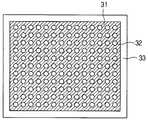
도 2는 종래의 건식식각 장치의 상부 전극에 대한 평면도.2 is a plan view of the upper electrode of the conventional dry etching device.
도 3은 본 발명의 제 1 실시예에 따른 건식식각 장치의 단면도.3 is a cross-sectional view of a dry etching apparatus according to a first embodiment of the present invention.
도 4는 본 발명의 제 1 실시예에 따른 건식식각 장치의 상부 전극에 대한 평면도.4 is a plan view of the upper electrode of the dry etching apparatus according to the first embodiment of the present invention.
도 5는 본 발명의 제 2 실시예에 따른 건식식각 장치의 단면도.5 is a cross-sectional view of a dry etching apparatus according to a second embodiment of the present invention.
도 6은 본 발명의 제 2 실시예에 따른 건식식각 장치의 상부 전극에 대한 평면도.
6 is a plan view of the upper electrode of the dry etching apparatus according to the second embodiment of the present invention.
<도면의 주요부분에 대한 부호의 설명><Description of the symbols for the main parts of the drawings>
110 : 챔버111 : 배기구110: chamber 111: exhaust port
112 : 가스주입구121 : 하부 전극112
122 : 기판123 : 하부 실드122: substrate 123: lower shield
131 : 상부 전극 132 : 노즐131: upper electrode 132: nozzle
133 : 상부 실드133: upper shield
본 발명은 반도체 소자의 제조 장치에 관한 것으로서, 더욱 상세하게는 박막의 건식식각 장치에 관한 것이다.The present invention relates to a device for manufacturing a semiconductor device, and more particularly to a dry etching device of a thin film.
최근 정보화 사회로 시대가 급발전함에 따라 고밀도의 집적회로 제작 및 박형화, 경량화, 저 소비전력화 등의 우수한 특성을 가지는 평판 표시 장치(flat panel display)의 필요성이 대두되었다.Recently, with the rapid development of the information society, the necessity of a flat panel display having excellent characteristics such as high density integrated circuit fabrication, thinning, light weight, and low power consumption has emerged.
집적회로는 그 집적도에 따라 고밀도 집적회로(large scale integration ; LSI)와 초고밀도 집적회로(very large scale integration ; VLSI) 등으로 나누어진다.Integrated circuits are classified into large scale integration (LSI), very large scale integration (VLSI), and the like according to their integration degree.
한편, 평판 표시 장치 중 해상도, 컬러표시, 화질 등의 장점을 가지는 액정 표시 장치(liquid crystal display)가 널리 이용되고 있는데, 액정 표시 장치는 다수의 박막 트랜지스터가 배열되어 있는 어레이 기판을 포함한다.On the other hand, a liquid crystal display (liquid crystal display) having advantages such as resolution, color display, image quality, etc. of the flat panel display device is widely used, the liquid crystal display includes an array substrate in which a plurality of thin film transistors are arranged.
이러한 액정 표시 장치의 어레이 기판 및 고밀도 집적회로는 박막을 증착하고 사진 식각하는 공정을 반복함으로써 이루어진다.An array substrate and a high density integrated circuit of such a liquid crystal display device are formed by repeating a process of depositing and photographic etching a thin film.
사진 식각은 감광막(photoresist)의 도포 및 베이킹, 노광, 현상, 그리고 박막의 식각으로 이루어지는데, 박막의 식각방법은 가스 플라즈마를 이용한 건식식각(dry etching)법과 화학용액을 이용한 습식식각(wet etching)법으로 크게 나누어진다.Photolithography consists of application and baking of photoresist, exposure, development, and etching of thin films. The etching methods of thin films are dry etching using gas plasma and wet etching using chemical solution. It is largely divided by law.
습식식각법은 주로 배선에 사용되는 금속막이나 화소 전극에 사용되는 인듐-틴-옥사이드(indium-tin-oxide ; ITO)의 패턴 형성에 적용되며, 양호한 선택비(selectivity)와 대면적에서의 식각 균일도, 생산성 등이 우수하고 저가격화가 가능하며, 세정 효과를 동시에 얻을 수 있는 장점이 있다.Wet etching is mainly applied to the formation of indium-tin-oxide (ITO) patterns used for metal films or pixel electrodes used for wiring, and has good selectivity and large area etching. It is excellent in uniformity, productivity and the like, and it is possible to reduce the price and to obtain a cleaning effect at the same time.
이러한 습식식각법은 디핑(dipping) 방식과 스프레이(spray) 방식이 있는데, 디핑 방식은 기판을 화학 용액에 담그는 방식이고, 스프레이 방식은 화학 용액을 기판에 뿌려주는 방식으로, 이들을 혼합하여 사용하기도 한다.These wet etching methods include a dipping method and a spray method. The dipping method is a method of dipping a substrate in a chemical solution, and the spray method is a method in which a chemical solution is sprayed onto a substrate. .
박막을 디핑 방식으로 식각할 경우, 여러 장의 기판을 하나의 용기(bath)에 넣어 한번에 공정을 진행하는 배치(batch) 방식을 이용할 수 있는데, 이는 대량 생산이 가능하여 제조 비용을 절감할 수 있다.When the thin film is etched by a dipping method, a batch method in which a plurality of substrates are placed in a bath and processed at a time may be used. This may allow mass production to reduce manufacturing costs.
한편, 건식식각법은 절연막이나 반도체층의 패턴 형성시 주로 이용되며, 패턴의 정밀도가 습식식각법에 비해 우수하다.On the other hand, the dry etching method is mainly used when forming the pattern of the insulating film or the semiconductor layer, the pattern accuracy is superior to the wet etching method.
이러한 건식식각법에서는, 챔버(chamber)에 유입된 반응가스가 일정 압력하에서 플라즈마 방전되는데, 이때 생성된 이온이나 라디칼(radical)에 의해 물리적 충돌이나 화학적 반응으로 박막의 식각이 이루어진다.In such a dry etching method, the reaction gas introduced into the chamber is plasma discharged under a constant pressure, and the thin film is etched by physical collision or chemical reaction by the generated ions or radicals.
건식식각법은 반응 방식에 따라 플라즈마 식각(plasma etching) 방식과 반응성 이온 식각(reactive ion etching) 방식으로 나눌 수 있다.Dry etching may be classified into a plasma etching method and a reactive ion etching method according to a reaction method.
플라즈마 식각 방식은 생성된 반응 물질 중 주로 라디칼이 화학적 반응에 의하여 식각에 이용된다. 라디칼은 분자가 여기된 중성 상태이기 때문에 전기장 방향에 영향을 받지 않는다. 따라서, 전기장 방향에 관계없이 식각비(etching ratio)가 동일하여 등방성(isotropy) 식각 양상을 보이며, 물리적 충돌이 적어 하부막에 대한 영향이 적고 선택적 식각에 유리하다.In the plasma etching method, mainly radicals of the generated reactants are used for etching by chemical reaction. The radicals are not affected by the direction of the electric field because the molecules are in a neutral state where they are excited. Therefore, the etching ratio is the same regardless of the electric field direction (isotropy) etching, the physical impact is small, there is little effect on the lower layer is advantageous for selective etching.
이에 비해, 반응성 이온 식각은 생성된 반응 물질 중 주로 이온이 전기장에 의해 가속되어 박막과 충돌함으로써 식각되는데, 이온은 전기장 방향으로 가속운동을 하므로 식각비가 방향에 따라 다르기 때문에, 이방성(anisotropy) 식각이 이루어진다.In contrast, reactive ion etching is mainly performed by etching ions accelerated by an electric field and colliding with a thin film. However, since an etch ratio varies depending on the direction since ions accelerate in an electric field direction, anisotropy etching is performed. Is done.
이하, 첨부한 도면을 참조하여 플라즈마를 이용한 종래의 건식식각 장치에 대하여 설명한다.Hereinafter, a conventional dry etching apparatus using plasma will be described with reference to the accompanying drawings.
건식식각 장치는 처리되는 대상물을 가지는 밀폐된 반응용기인 챔버와, 챔버로 인입되는 기체물질을 저장하고 이를 챔버 내부로 유입하는 가스 도입부, 그리고 가스 도입부로부터 유입되는 기체물질을 챔버내에서 플라즈마로 변화시키기 위하여 챔버 내부와 전기적으로 연결되는 전력 공급부로 이루어진다.The dry etching apparatus includes a chamber, which is a sealed reaction container having an object to be treated, a gas inlet for storing gas material introduced into the chamber and introducing the gas material into the chamber, and a gas material flowing from the gas inlet into plasma in the chamber. It consists of a power supply that is electrically connected to the inside of the chamber to make.
도 1은 종래의 건식식각 장치의 챔버를 도시한 단면도이고, 도 2는 종래의 건식식각 장치의 상부 전극 부분에 대한 평면도이다.1 is a cross-sectional view illustrating a chamber of a conventional dry etching apparatus, and FIG. 2 is a plan view of an upper electrode portion of a conventional dry etching apparatus.
도시한 바와 같이, 반응용기인 챔버(10)의 상면에는 가스 도입부(도시하지 않음)로부터 반응가스를 챔버(10) 내부로 유입하기 위한 가스주입구(12)가 형성되어 있으며, 챔버(10)의 하면에는 챔버(10) 내부의 공기를 배출하기 위한 배기구(11)가 형성되어 있다. 챔버(10) 내에는 하부 전극(21)과 상부 전극(31)이 일정 간격을 가지고 배치되어 있으며, 두 전극(21, 31) 사이의 공간은 반응영역이 된다. 상부 전극(31)은 접지되어 있으며, 다수 개의 홀(32)을 가지고 있고, 상부 전극(31) 위에는 제 1 내지 제 3 가스 분사판(41, 42, 43)이 각각 배치되어 있는데, 제 1 내지 제 3 가스 분사판(41, 42, 43)은 가스주입구(12)를 통해 챔버(10) 내부로 유입된 가스의 분포를 고르게 하기 위한 것이다. 따라서, 챔버(10) 내로 유입된 가스는 가스 분사판(41, 42, 43)을 통해 고른 분포로 상부 전극(31)에 전달되고, 상부 전극(31)의 홀을 통해 상부 전극(31)과 하부 전극(21) 사이의 반응영역으로 확산되어 보내진다.As shown, a
다음, 하부 전극(21) 상에는 처리되는 대상물 즉, 패터닝될 박막을 포함하는 기판(22)이 안치된다. 하부 전극(21)은 외부의 전력 공급부와 연결되어 무선주파수(radio frequency)를 가지는 전압이 인가된다.Next, the
하부 전극(21) 및 상부 전극(31)의 둘레에는 차폐물인 실드(shield)(23, 33)가 형성되어 있는데, 특히 상부 실드(33)는 일부가 반응영역 내에까지 연장되어 있어, 플라즈마 밀도가 기판(22)에 대응하는 부분에서 높아지도록 하는 역할을 한다.Shields 23 and 33, which are shields, are formed around the
이와 같은 건식식각 장치에서는 상부 전극(31)에 다수의 홀(32)이 형성되어 있으므로, 가스의 분사를 고르게 하여 플라즈마 밀도를 균일하게 할 수 있으나, 제 1 내지 제 3 가스 분사판(41, 42, 43)과 같은 분사판이 필요하고, 이러한 가스 분사판(41, 42, 43)은 구조가 복잡하여 제조하는데 있어 많은 비용이 드는 단점이 있다.In the dry etching apparatus, since the plurality of
한편, 일반적으로 건식식각 장치의 전극 재료로는 알루미늄(aluminium)을 사용하며, 반응가스에 의해 전극이 부식되는 것을 방지하기 위해 양극산화시켜 전극의 표면에 얇은 보호막을 형성한다. 그런데, 이러한 보호막은 홀(32) 부분에서 결 합력이 약하기 때문에, 플라즈마 발생시 홀(32) 부분에서 크랙(crack)이 발생하며 또한 일부가 분리되어 기판(도 1의 22) 상에 떨어지게 되므로, 식각 불량이 나타나게 된다.
In general, aluminum is used as an electrode material of a dry etching apparatus, and in order to prevent corrosion of the electrode by the reaction gas, anodization is performed to form a thin protective film on the surface of the electrode. However, since the passivation layer has a weak bonding force in the
본 발명은 상기한 종래의 문제점을 해결하기 위해 안출된 것으로서, 본 발명의 목적은 반응 가스가 전극 외곽에서 분사되도록 함으로써, 전극의 보호막에 의한 식각 불량을 방지할 수 있는 건식식각 장치를 제공하는 것이다.The present invention has been made to solve the above-mentioned conventional problems, an object of the present invention is to provide a dry etching apparatus that can prevent the etching failure by the protective film of the electrode by allowing the reaction gas is injected from the outer electrode. .
본 발명의 다른 목적은 구조가 간단하며 제조 비용을 감소시킬 수 있는 건식식각 장치를 제공하는 것이다.
It is another object of the present invention to provide a dry etching apparatus which is simple in structure and which can reduce manufacturing costs.
상기한 목적을 달성하기 위한 본 발명에 따른 건식식각 장치는 챔버와 챔버 내부에 위치하는 상부 전극, 그리고 상부 전극과 이격되어 위치하고 처리되는 대상물이 안치되는 하부 전극과, 반응가스를 챔버 내부로 유입하는 가스유입부, 상부전극 외곽에 위치하며 가스유입부로부터의 가스를 상부전극과 하부전극 사이로 전달하는 노즐과, 챔버 내부의 공기를 배출시키기 위한 배기부, 그리고 상부 전극 및 하부 전극과 연결되어 있는 전력 공급부를 포함한다.Dry etching apparatus according to the present invention for achieving the above object is the chamber and the upper electrode located inside the chamber, and the lower electrode spaced apart from the upper electrode and the object to be placed, the reaction gas is introduced into the chamber Gas inlet, located outside the upper electrode, a nozzle for transferring gas from the gas inlet between the upper electrode and the lower electrode, an exhaust for discharging air in the chamber, and the power connected to the upper electrode and the lower electrode It includes a supply.
여기서, 건식식각 장치는 상부전극 둘레에 세라믹으로 이루어진 실드를 더 포함할 수 있다.Here, the dry etching apparatus may further include a shield made of ceramic around the upper electrode.
노즐은 상부 전극과 실드 사이에 위치할 수 있으며, 또는 실드 바깥쪽에 위치할 수도 있다.The nozzle may be located between the top electrode and the shield, or may be located outside the shield.
이와 같이, 본 발명에 따른 건식식각 장치에서는 상부 전극 외곽에 다수의 노즐을 형성하여 반응가스를 분사함으로써, 플라즈마 발생시 상부 전극의 보호막에 크랙이 발생하는 것을 방지하고, 보호막에 의한 불순물의 발생도 막을 수 있으며, 또한, 가스 분사를 위한 장치의 구조가 간단하고 제조 비용을 감소시킬 수도 있다.As described above, in the dry etching apparatus according to the present invention, a plurality of nozzles are formed outside the upper electrode to inject the reaction gas, thereby preventing cracks in the protective film of the upper electrode during plasma generation, and preventing the generation of impurities by the protective film. In addition, the structure of the device for gas injection can be simple and reduce the manufacturing cost.
이하, 첨부한 도면을 참조하여 본 발명의 실시예에 따른 건식식각 장치에 대하여 상세히 설명한다.Hereinafter, a dry etching apparatus according to an exemplary embodiment of the present invention will be described in detail with reference to the accompanying drawings.
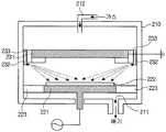
도 3은 본 발명에 따른 건식식각 장치의 단면도이고, 도 4는 본 발명에 따른 건식식각 장치의 상부 전극 부분에 대한 평면도이다.3 is a cross-sectional view of a dry etching apparatus according to the present invention, Figure 4 is a plan view of the upper electrode portion of the dry etching apparatus according to the present invention.
도시한 바와 같이, 도시한 바와 같이, 반응용기인 챔버(110)의 상면에는 가스 도입부(도시하지 않음)로부터 반응가스를 챔버(110) 내부로 유입하기 위한 가스주입구(112)가 형성되어 있으며, 챔버(110)의 하면에는 챔버(110) 내부의 공기를 배출하기 위한 배기구(111)가 형성되어 있다. 챔버(110) 내에는 하부 전극(121)과 상부 전극(131)이 일정 간격을 가지고 배치되어 있으며, 두 전극(121, 131)의 사이 공간은 플라즈마가 생성되는 반응영역이 된다. 상부 전극(131)은 접지되어 있고, 상부 전극(131) 둘레에는 세라믹과 같은 물질로 이루어진 실드(133)가 형성되어 있으며, 상부 전극(131)과 실드(133) 사이에는 다수의 노즐(nozzle)(132)이 형성되어 있다. 여기서, 실드(133)는 일부가 반응영역 내에 위치하는 구조로 이루어져 플라즈마가 퍼지는 것을 막으며, 노즐(132)은 실드(133)의 형태를 따라 'ㄴ'자 형태를 이룬다.As shown, as shown, a
다음, 하부 전극(121) 상에는 처리되는 대상물 즉, 패터닝될 박막을 포함하는 기판(122)이 안치된다. 하부 전극(121)은 외부의 전력 공급부와 연결되어 무선주파수를 가지는 전압이 인가되며, 하부 전극(121) 둘레에는 세라믹으로 이루어진 차폐물인 실드(123)가 형성되어 있다.Next, a
본 발명에서 상부 전극(131)과 하부 전극(121)은 알루미늄으로 형성할 수 있으며, 플라즈마에 의해 부식되는 것을 방지하기 위해 양극산화시켜 보호막을 형성하는 것이 좋다.In the present invention, the
한편, 본 발명에서는 가스 분사의 균일도를 높이기 위해 노즐(132)의 끝단을 조절하여, 노즐(132) 끝단이 기판(122) 상면을 골고루 향하도록 한다.Meanwhile, in the present invention, the end of the
따라서, 본 발명에서는 상부 전극에 가스 분사를 위한 홀을 형성하지 않기 때문에, 상부 전극 표면의 보호막이 분리되어 떨어지는 것을 방지할 수 있으며, 끝의 작은 구멍으로부터 유체를 분출시키는 노즐을 통해 가스를 분사함으로써, 플라즈마 밀도의 균일도가 저하되는 것을 막을 수 있다.Therefore, in the present invention, since the hole for gas injection is not formed in the upper electrode, the protective film on the surface of the upper electrode can be prevented from falling off, and by injecting gas through a nozzle that ejects the fluid from the small hole at the end. The fall of the uniformity of plasma density can be prevented.
앞선 실시예에서는 노즐을 상부 전극과 실드 사이에 배치하였으나, 노즐을 실드 바깥쪽에 배치할 수도 있는데, 이러한 본 발명의 제 2 실시예에 따른 건식식각 장치의 단면도 및 상부 전극 부분의 평면도를 도 5와 도 6에 각각 도시하였다. 제 2 실시예는 노즐의 위치를 제외하면, 앞선 제 1 실시예와 동일한 구조를 가지므로 간략하게 설명하기로 한다.In the above embodiment, although the nozzle is disposed between the upper electrode and the shield, the nozzle may be disposed outside the shield. The cross-sectional view of the dry etching apparatus according to the second embodiment of the present invention and a plan view of the upper electrode portion are shown in FIGS. 6, respectively. Since the second embodiment has the same structure as the first embodiment except for the position of the nozzle, it will be briefly described.
도시한 바와 같이 하부의 배기구(211)와 상부의 가스주입구(212)를 가지는 챔버(210) 내에 상부 전극(231)과 하부 전극(221)이 일정 간격을 가지고 배치되어 있고, 하부 전극(221)의 상부에는 시료인 기판(222)이 안치되어 있다. 하부 전극(221) 및 상부 전극(231) 둘레에는 세라믹으로 이루어진 실드(223, 233)가 하부 전극(221)과 상부 전극(231)을 둘러싸고 있으며, 상부 실드(233) 바깥쪽에는 다수의 노즐(232)이 형성되어 실드(233)를 둘러싸고 있다.As shown in the drawing, the
여기서도 가스 분사의 균일도를 높이기 위해 노즐(232)의 끝단이 기판(222) 상면을 골고루 향하도록 하는 것이 좋다.Here, in order to increase the uniformity of the gas injection, the end of the
본 발명은 상기한 실시예에 한정되지 아니하며, 본 발명의 정신을 벗어나지 않는 이상 다양한 변화와 변형이 가능하다.
The present invention is not limited to the above embodiments, and various changes and modifications can be made without departing from the spirit of the present invention.
본 발명에 따른 건식식각 장치에서는 상부 전극 외곽에 다수의 노즐을 형성하여 반응가스를 분사함으로써, 플라즈마 발생시 상부 전극의 보호막에 크랙이 발생하는 것을 방지하고, 보호막에 의한 불순물의 발생도 막을 수 있다. 또한, 가스 분사를 위한 장치의 구조가 간단하며 제조 비용을 감소시킬 수 있다.
In the dry etching apparatus according to the present invention, by forming a plurality of nozzles around the upper electrode and injecting the reaction gas, cracks may be prevented from occurring in the protective film of the upper electrode during plasma generation, and generation of impurities by the protective film may be prevented. In addition, the structure of the device for gas injection is simple and the manufacturing cost can be reduced.
Claims (5)
Translated fromKoreanPriority Applications (1)
| Application Number | Priority Date | Filing Date | Title |
|---|---|---|---|
| KR1020010050645AKR100780285B1 (en) | 2001-08-22 | 2001-08-22 | Dry etching equipment |
Applications Claiming Priority (1)
| Application Number | Priority Date | Filing Date | Title |
|---|---|---|---|
| KR1020010050645AKR100780285B1 (en) | 2001-08-22 | 2001-08-22 | Dry etching equipment |
Publications (2)
| Publication Number | Publication Date |
|---|---|
| KR20030016864A KR20030016864A (en) | 2003-03-03 |
| KR100780285B1true KR100780285B1 (en) | 2007-11-28 |
Family
ID=27720275
Family Applications (1)
| Application Number | Title | Priority Date | Filing Date |
|---|---|---|---|
| KR1020010050645AExpired - Fee RelatedKR100780285B1 (en) | 2001-08-22 | 2001-08-22 | Dry etching equipment |
Country Status (1)
| Country | Link |
|---|---|
| KR (1) | KR100780285B1 (en) |
Citations (6)
| Publication number | Priority date | Publication date | Assignee | Title |
|---|---|---|---|---|
| JPH03188627A (en)* | 1989-12-18 | 1991-08-16 | Sharp Corp | plasma etching equipment |
| KR960032629A (en)* | 1995-02-07 | 1996-09-17 | 야스까와 히데아끼 | Method and apparatus for removing unnecessary material around substrate and method of applying using same |
| KR100284571B1 (en)* | 1995-12-22 | 2001-04-02 | 조셉 제이. 스위니 | Apparatus and method for reducing residue buildup in CVD chamber using ceramic lining |
| KR20010039218A (en)* | 1999-10-29 | 2001-05-15 | 윤종용 | Method and apparatus for etching semiconductor wafer |
| KR20020031997A (en)* | 2000-10-25 | 2002-05-03 | 김정곤 | High density plasma oxide film etching apparatus |
| KR20020093214A (en)* | 2001-06-07 | 2002-12-16 | 삼성전자 주식회사 | Upper electrode constuction of semiconductor etch device |
- 2001
- 2001-08-22KRKR1020010050645Apatent/KR100780285B1/ennot_activeExpired - Fee Related
Patent Citations (6)
| Publication number | Priority date | Publication date | Assignee | Title |
|---|---|---|---|---|
| JPH03188627A (en)* | 1989-12-18 | 1991-08-16 | Sharp Corp | plasma etching equipment |
| KR960032629A (en)* | 1995-02-07 | 1996-09-17 | 야스까와 히데아끼 | Method and apparatus for removing unnecessary material around substrate and method of applying using same |
| KR100284571B1 (en)* | 1995-12-22 | 2001-04-02 | 조셉 제이. 스위니 | Apparatus and method for reducing residue buildup in CVD chamber using ceramic lining |
| KR20010039218A (en)* | 1999-10-29 | 2001-05-15 | 윤종용 | Method and apparatus for etching semiconductor wafer |
| KR20020031997A (en)* | 2000-10-25 | 2002-05-03 | 김정곤 | High density plasma oxide film etching apparatus |
| KR20020093214A (en)* | 2001-06-07 | 2002-12-16 | 삼성전자 주식회사 | Upper electrode constuction of semiconductor etch device |
Also Published As
| Publication number | Publication date |
|---|---|
| KR20030016864A (en) | 2003-03-03 |
Similar Documents
| Publication | Publication Date | Title |
|---|---|---|
| US5100476A (en) | Method and apparatus for cleaning semiconductor devices | |
| JPH07142449A (en) | Plasma etching equipment | |
| US20040253896A1 (en) | Method of manufacturing display device | |
| CN102034666A (en) | Side gas injector for plasma reaction chamber | |
| JPH08279468A (en) | Method and apparatus of treatment | |
| CN1327481C (en) | Method of forming multilayer interconnection structure, method of manufacturing circuit board, and method of manufacturing device | |
| CN108321101A (en) | Electrode assembly and etching equipment | |
| US20160115595A1 (en) | Gas supply apparatus | |
| KR100780285B1 (en) | Dry etching equipment | |
| JPH09223685A (en) | Plasma processing apparatus and plasma processing method | |
| KR100688229B1 (en) | Dry etching equipment | |
| TWI886278B (en) | Apparatus for processing substrate | |
| KR20050023083A (en) | Apparatus for wet etching of insulating glass substrate and method for wet etching the same | |
| KR101016921B1 (en) | Shower head | |
| US20010015210A1 (en) | Wet etching apparatus and method | |
| JPS58164786A (en) | How to form electrodes | |
| KR100621788B1 (en) | Ozone asher device | |
| JP2006019750A (en) | Substrate processing equipment | |
| KR100641840B1 (en) | Shower Head and Plasma Processing Equipment | |
| KR100209731B1 (en) | Cleaning apparatus for semiconductor wafer | |
| KR19980045169A (en) | Shower head of semiconductor manufacturing apparatus and manufacturing method thereof | |
| KR101001018B1 (en) | Shower nozzle adjustment system | |
| KR100453015B1 (en) | Surface treatment method and apparatus, surface treatment method of substrate and manufacturing method of substrate | |
| KR20020048128A (en) | apparatus and method for etching | |
| KR20060058228A (en) | Ultrasonic Cleaning Device of Plasma Display Panel |
Legal Events
| Date | Code | Title | Description |
|---|---|---|---|
| PA0109 | Patent application | St.27 status event code:A-0-1-A10-A12-nap-PA0109 | |
| P11-X000 | Amendment of application requested | St.27 status event code:A-2-2-P10-P11-nap-X000 | |
| P13-X000 | Application amended | St.27 status event code:A-2-2-P10-P13-nap-X000 | |
| PG1501 | Laying open of application | St.27 status event code:A-1-1-Q10-Q12-nap-PG1501 | |
| A201 | Request for examination | ||
| P11-X000 | Amendment of application requested | St.27 status event code:A-2-2-P10-P11-nap-X000 | |
| P13-X000 | Application amended | St.27 status event code:A-2-2-P10-P13-nap-X000 | |
| PA0201 | Request for examination | St.27 status event code:A-1-2-D10-D11-exm-PA0201 | |
| R17-X000 | Change to representative recorded | St.27 status event code:A-3-3-R10-R17-oth-X000 | |
| D13-X000 | Search requested | St.27 status event code:A-1-2-D10-D13-srh-X000 | |
| D14-X000 | Search report completed | St.27 status event code:A-1-2-D10-D14-srh-X000 | |
| E902 | Notification of reason for refusal | ||
| PE0902 | Notice of grounds for rejection | St.27 status event code:A-1-2-D10-D21-exm-PE0902 | |
| P11-X000 | Amendment of application requested | St.27 status event code:A-2-2-P10-P11-nap-X000 | |
| P13-X000 | Application amended | St.27 status event code:A-2-2-P10-P13-nap-X000 | |
| E701 | Decision to grant or registration of patent right | ||
| PE0701 | Decision of registration | St.27 status event code:A-1-2-D10-D22-exm-PE0701 | |
| GRNT | Written decision to grant | ||
| PR0701 | Registration of establishment | St.27 status event code:A-2-4-F10-F11-exm-PR0701 | |
| PR1002 | Payment of registration fee | St.27 status event code:A-2-2-U10-U11-oth-PR1002 Fee payment year number:1 | |
| PG1601 | Publication of registration | St.27 status event code:A-4-4-Q10-Q13-nap-PG1601 | |
| G170 | Re-publication after modification of scope of protection [patent] | ||
| PG1701 | Publication of correction | St.27 status event code:A-5-5-P10-P19-oth-PG1701 Patent document republication publication date:20080415 Republication note text:Request for Correction Notice (Document Request) Gazette number:1007802850000 Gazette reference publication date:20071128 | |
| PN2301 | Change of applicant | St.27 status event code:A-5-5-R10-R13-asn-PN2301 St.27 status event code:A-5-5-R10-R11-asn-PN2301 | |
| PR1001 | Payment of annual fee | St.27 status event code:A-4-4-U10-U11-oth-PR1001 Fee payment year number:4 | |
| R18-X000 | Changes to party contact information recorded | St.27 status event code:A-5-5-R10-R18-oth-X000 | |
| PR1001 | Payment of annual fee | St.27 status event code:A-4-4-U10-U11-oth-PR1001 Fee payment year number:5 | |
| R18-X000 | Changes to party contact information recorded | St.27 status event code:A-5-5-R10-R18-oth-X000 | |
| R18-X000 | Changes to party contact information recorded | St.27 status event code:A-5-5-R10-R18-oth-X000 | |
| FPAY | Annual fee payment | Payment date:20120928 Year of fee payment:6 | |
| PR1001 | Payment of annual fee | St.27 status event code:A-4-4-U10-U11-oth-PR1001 Fee payment year number:6 | |
| FPAY | Annual fee payment | Payment date:20130930 Year of fee payment:7 | |
| PR1001 | Payment of annual fee | St.27 status event code:A-4-4-U10-U11-oth-PR1001 Fee payment year number:7 | |
| FPAY | Annual fee payment | Payment date:20141021 Year of fee payment:8 | |
| PR1001 | Payment of annual fee | St.27 status event code:A-4-4-U10-U11-oth-PR1001 Fee payment year number:8 | |
| FPAY | Annual fee payment | Payment date:20151028 Year of fee payment:9 | |
| PR1001 | Payment of annual fee | St.27 status event code:A-4-4-U10-U11-oth-PR1001 Fee payment year number:9 | |
| FPAY | Annual fee payment | Payment date:20161012 Year of fee payment:10 | |
| PR1001 | Payment of annual fee | St.27 status event code:A-4-4-U10-U11-oth-PR1001 Fee payment year number:10 | |
| FPAY | Annual fee payment | Payment date:20171016 Year of fee payment:11 | |
| PR1001 | Payment of annual fee | St.27 status event code:A-4-4-U10-U11-oth-PR1001 Fee payment year number:11 | |
| P22-X000 | Classification modified | St.27 status event code:A-4-4-P10-P22-nap-X000 | |
| FPAY | Annual fee payment | Payment date:20181015 Year of fee payment:12 | |
| PR1001 | Payment of annual fee | St.27 status event code:A-4-4-U10-U11-oth-PR1001 Fee payment year number:12 | |
| PC1903 | Unpaid annual fee | St.27 status event code:A-4-4-U10-U13-oth-PC1903 Not in force date:20191123 Payment event data comment text:Termination Category : DEFAULT_OF_REGISTRATION_FEE | |
| PC1903 | Unpaid annual fee | St.27 status event code:N-4-6-H10-H13-oth-PC1903 Ip right cessation event data comment text:Termination Category : DEFAULT_OF_REGISTRATION_FEE Not in force date:20191123 |