KR100777570B1 - Pollution measuring device of rapid thermal processing chamber - Google Patents
Pollution measuring device of rapid thermal processing chamberDownload PDFInfo
- Publication number
- KR100777570B1 KR100777570B1KR1020060114920AKR20060114920AKR100777570B1KR 100777570 B1KR100777570 B1KR 100777570B1KR 1020060114920 AKR1020060114920 AKR 1020060114920AKR 20060114920 AKR20060114920 AKR 20060114920AKR 100777570 B1KR100777570 B1KR 100777570B1
- Authority
- KR
- South Korea
- Prior art keywords
- laser beam
- thermal processing
- contamination
- processing chamber
- rapid thermal
- Prior art date
- Legal status (The legal status is an assumption and is not a legal conclusion. Google has not performed a legal analysis and makes no representation as to the accuracy of the status listed.)
- Expired - Fee Related
Links
Images


Classifications
- H—ELECTRICITY
- H01—ELECTRIC ELEMENTS
- H01L—SEMICONDUCTOR DEVICES NOT COVERED BY CLASS H10
- H01L21/00—Processes or apparatus adapted for the manufacture or treatment of semiconductor or solid state devices or of parts thereof
- H01L21/67—Apparatus specially adapted for handling semiconductor or electric solid state devices during manufacture or treatment thereof; Apparatus specially adapted for handling wafers during manufacture or treatment of semiconductor or electric solid state devices or components ; Apparatus not specifically provided for elsewhere
- H01L21/67005—Apparatus not specifically provided for elsewhere
- H01L21/67242—Apparatus for monitoring, sorting or marking
- H—ELECTRICITY
- H01—ELECTRIC ELEMENTS
- H01L—SEMICONDUCTOR DEVICES NOT COVERED BY CLASS H10
- H01L21/00—Processes or apparatus adapted for the manufacture or treatment of semiconductor or solid state devices or of parts thereof
- H01L21/02—Manufacture or treatment of semiconductor devices or of parts thereof
- H01L21/04—Manufacture or treatment of semiconductor devices or of parts thereof the devices having potential barriers, e.g. a PN junction, depletion layer or carrier concentration layer
- H01L21/18—Manufacture or treatment of semiconductor devices or of parts thereof the devices having potential barriers, e.g. a PN junction, depletion layer or carrier concentration layer the devices having semiconductor bodies comprising elements of Group IV of the Periodic Table or AIIIBV compounds with or without impurities, e.g. doping materials
- H01L21/30—Treatment of semiconductor bodies using processes or apparatus not provided for in groups H01L21/20 - H01L21/26
- H01L21/324—Thermal treatment for modifying the properties of semiconductor bodies, e.g. annealing, sintering
- H—ELECTRICITY
- H01—ELECTRIC ELEMENTS
- H01L—SEMICONDUCTOR DEVICES NOT COVERED BY CLASS H10
- H01L21/00—Processes or apparatus adapted for the manufacture or treatment of semiconductor or solid state devices or of parts thereof
- H01L21/67—Apparatus specially adapted for handling semiconductor or electric solid state devices during manufacture or treatment thereof; Apparatus specially adapted for handling wafers during manufacture or treatment of semiconductor or electric solid state devices or components ; Apparatus not specifically provided for elsewhere
- H01L21/67005—Apparatus not specifically provided for elsewhere
- H01L21/67011—Apparatus for manufacture or treatment
- H01L21/67098—Apparatus for thermal treatment
Landscapes
- Engineering & Computer Science (AREA)
- Physics & Mathematics (AREA)
- Condensed Matter Physics & Semiconductors (AREA)
- General Physics & Mathematics (AREA)
- Manufacturing & Machinery (AREA)
- Computer Hardware Design (AREA)
- Microelectronics & Electronic Packaging (AREA)
- Power Engineering (AREA)
- Testing Or Measuring Of Semiconductors Or The Like (AREA)
Abstract
Translated fromKoreanDescription
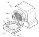
Translated fromKorean도 1은 일반적인 급속열처리공정챔버를 보여주는 사시도,1 is a perspective view showing a typical rapid heat treatment chamber;
도 2는 도 1의 내부 구성을 보여주는 단면도,2 is a cross-sectional view showing the internal configuration of FIG.
도 3은 본 발명에 따른 급속열처리공정챔버의 오염측정장치를 보여주는 개략적인 사시도,3 is a schematic perspective view showing a pollution measuring apparatus of a rapid heat treatment process chamber according to the present invention;
도 4는 본 발명에 따른 급속열처리공정챔버의 오염측정장치의 일 실시 예를 보여주는 개략적인 상태도이다.Figure 4 is a schematic state diagram showing an embodiment of the contamination measurement apparatus of the rapid thermal processing chamber according to the present invention.
<도면의 주요부분에 대한 부호의 설명><Description of the symbols for the main parts of the drawings>
100 : 급속열처리공정챔버 110 : 할로겐램프100: rapid heat treatment process chamber 110: halogen lamp
120 : 챔버베이스 130 : 골드플레이트120: chamber base 130: gold plate
150 : 옵틱프로브 210 : 발광센서부150: optical probe 210: light emitting sensor
220 : 수광센서부 230 : 반사거울220: light receiving sensor 230: reflection mirror
250 : 레이저빔 300 : 제어부250: laser beam 300: control unit
P : 레이저포인트P: laser point
본 발명은 급속열처리챔버의 오염측정장치에 관한 것으로, 더욱 상세하게는 급속열처리공정챔버 내부에 구성된 골드플레이트(Gold Plate)의 오염 정도를 실시간으로 측정해 줌으로써 장비의 효율적인 관리가 이루어질 수 있도록 한 급속열처리챔버의 오염측정장치에 관한 것이다.The present invention relates to a pollution measuring apparatus of a rapid heat treatment chamber. More particularly, the present invention relates to a rapid measurement process for efficiently managing equipment by measuring the degree of contamination of a gold plate configured in a rapid heat treatment chamber in real time. The present invention relates to an apparatus for measuring contamination of a heat treatment chamber.
일반적으로 화합물 반도체를 이용한 반도체소자 가공공정 중 기판에 원하는 불순물(Dopant)을 주입하는 방법으로는 통상 이온주입법이 사용된다. 상기 이온주입법에 의하여 이온주입이 된 기판은 결정구조가 파괴되기 때문에 어닐링(Annealing) 공정에 의하여 파괴된 결정을 재결정화하고 있다.In general, an ion implantation method is generally used as a method of injecting a desired dopant into a substrate during a semiconductor device processing process using a compound semiconductor. Since the crystal structure is destroyed in the substrate implanted by the ion implantation method, the crystal destroyed by the annealing process is recrystallized.
상기 어닐링(Annealing)은 급속열처리공정(RTP : Rapid Thermal Process)챔버 내에서 이루어지게 된다.The annealing is performed in a rapid thermal process (RTP) chamber.
도 1은 일반적인 급속열처리공정챔버를 보여주는 사시도이고, 도 2는 도 1의 내부 구성을 보여주는 단면도이다.1 is a perspective view showing a typical rapid heat treatment chamber, Figure 2 is a cross-sectional view showing the internal configuration of FIG.
도 1 및 도 2를 참조하면, 일반적인 급속열처리공정챔버(100)는 높은 열을 발생시켜 웨이퍼를 가열하는 다수개의 할로겐 램프(110)가 구성되고, 상기 할로겐 램프(110)의 하면에 웨이퍼가 위치하게 된다.Referring to FIGS. 1 and 2, a general rapid
상기 급속열처리공정챔버(100)의 챔버베이스(120) 내부에는 웨이퍼가 위치하게 되는 골드플레이트(130)가 구성되고, 상기 골드플레이트(130)에는 다수 개의 옵틱프로브(Optic Probe)(150)가 설치되어 있다.In the
상기 할로겐램프(110)에 의해 가열되는 웨이퍼는 복사열을 방출하게 된다. 이 경우 웨이퍼 하부에 위치하는 상기 옵틱프로브(150)에서는 복사열의 파장을 공정 온도로 인식하게 된다.The wafer heated by the
상기 다수개의 옵틱프로브(150)는 포지션별로 정해진 곳에 설치되어, 해당 옵틱프로브(150) 마다 복사파장을 각각 감지하여 온도를 측정하게 된다.The plurality of
이 경우 상기 골드플레이트(130)는 복사열을 잘 읽을 수 있도록 최대한 반사가 잘되는 재질로 되어 있다.In this case, the
그러나 상기 열처리공정 진행시 웨이퍼의 상태에 따라 오염물질이 발생하게 되며, 상기 발생한 오염물질은 복사열을 반사시키는 골드플레이트(130)에 영향을 주어 반사율을 떨어뜨리는 문제점이 있다.However, during the heat treatment process, contaminants are generated according to the state of the wafer, and the generated contaminants affect the
또한, 상기 골드플레이트(130)의 반사율이 떨어진 상태에선 옵틱프로브(150)가 정확한 온도를 측정하지 못하게 됨으로써, 결국 웨이퍼의 수율(Yield)이 저하되는 문제가 있다.In addition, when the reflectance of the
본 발명은 상술한 문제점을 해결하고자 안출된 것으로, 급속열처리공정챔버 내부에 구성된 골드플레이트(Gold Plate)의 오염 정도를 실시간으로 측정해 줌으로써 장비의 효율적인 관리가 이루어질 수 있도록 한 급속열처리공정챔버의 오염측정장치를 제공하는데 그 목적이 있다.The present invention has been made to solve the above-mentioned problems, the contamination of the rapid heat treatment chamber to measure the degree of contamination of the gold plate (Gold Plate) configured inside the rapid heat treatment chamber in real time to enable efficient management of equipment The purpose is to provide a measuring device.
상술한 바와 같은 목적을 구현하기 위한 본 발명의 급속열처리공정챔버의 오염측정장치는,The contamination measuring apparatus of the rapid thermal processing chamber of the present invention for achieving the above object,
이온주입층이 형성된 기판을 어닐링(Annealing)하기 위해 열을 발생시키는 다수개의 할로겐 램프와, 웨이퍼가 위치되는 골드플레이트를 포함하여 구성된 급속열처리공정챔버의 오염측정장치에 있어서,In the contamination measurement apparatus of the rapid thermal processing chamber comprising a plurality of halogen lamps for generating heat to anneal the substrate on which the ion implantation layer is formed, and a gold plate on which the wafer is located,
상기 급속열처리공정챔버 내부의 일 측면에 설치되어 골드플레이트의 표면에 레이저빔을 발생시키는 발광센서부; 상기 발광센서부에서 발생한 레이저빔을 굴절시키는 반사거울; 상기 반사거울을 통해 굴절된 레이저빔을 감지하는 수광센서부; 상기 레이저빔의 감도를 통하여 급속열처리공정챔버 내부의 오염 정도를 측정하는 제어부; 를 포함하는 것을 특징으로 한다.A light emitting sensor unit installed at one side of the rapid heat treatment chamber to generate a laser beam on a surface of the gold plate; A reflection mirror that refracts the laser beam generated by the light emitting sensor unit; A light receiving sensor unit configured to detect a laser beam refracted through the reflection mirror; A control unit for measuring the degree of contamination inside the rapid thermal processing chamber through the sensitivity of the laser beam; Characterized in that it comprises a.
또한, 상기 반사거울은 적어도 하나 이상으로 설치되는 것을 특징으로 한다.In addition, the reflective mirror is characterized in that at least one is installed.
또한, 상기 제어부에서 측정된 오염 수치는 실시간으로 모니터링되는 것을 특징으로 한다.In addition, the contamination value measured by the control unit is characterized in that the monitoring in real time.
이하 첨부한 도면을 참조하여 본 발명의 바람직한 실시 예에 대한 구성 및 작용을 상세히 설명하면 다음과 같다.Hereinafter, the configuration and operation of the preferred embodiment of the present invention will be described in detail with reference to the accompanying drawings.
여기서, 종래 구성과 동일한 부분에 대해서는 동일한 부호 및 명칭을 사용한다.Here, about the same part as a conventional structure, the same code | symbol and name are used.
도 3은 본 발명에 따른 급속열처리공정챔버의 오염측정장치를 보여주는 개략적인 사시도이고, 도 4는 본 발명에 따른 급속열처리공정챔버의 오염측정장치의 일 실시 예를 보여주는 개략적인 상태도이다.3 is a schematic perspective view showing a contamination measurement apparatus of a rapid heat treatment chamber according to the present invention, Figure 4 is a schematic state diagram showing an embodiment of a pollution measurement apparatus of a rapid heat treatment chamber according to the present invention.
본 발명의 일 실시 예에 따른 급속열처리공정챔버의 오염측정장치는, 급속열처리공정챔버(100)의 내부에 구성되어 웨이퍼를 가열하는 다수개의 할로겐 램프(110)와, 웨이퍼가 위치하게 되는 골드플레이트(130)와, 상기 골드플레이트(130)에 설치되어 복사열의 파장을 공정 온도로 인식하는 다수 개의 옵틱프로브(Optic Probe)(150)의 구성은 종래의 기술과 동일하므로 설명의 중복을 피하기 위하여 상세한 설명은 생략하고, 새로이 부가되는 구성 부재들의 동작을 중심으로 하여 상세히 설명한다.The pollution measuring apparatus of the rapid thermal processing chamber according to an embodiment of the present invention, the plurality of
상기 급속열처리공정챔버(100)에서 공정이 진행되는 과정에서 발생하는 오염물질은 복사열을 반사시키는 골드플레이트(130)의 반사율을 떨어뜨리게 된다. 따라서, 상기 골드플레이트(130)의 오염 정도를 작업자가 인식하여 장비의 주기적인 관리가 이루어질 수 있는 구조가 마련되어야 한다.Contaminants generated during the process in the rapid
이를 구현하기 위한 실시 예를 설명하기 위하여 도 3을 참조하면, 본 발명에 따른 급속열처리공정챔버의 오염측정장치는 센서부(200), 반사거울(230) 및 제어부(300)를 포함하여 구성된다.Referring to Figure 3 to describe an embodiment for implementing this, the pollution measuring apparatus of the rapid thermal processing chamber according to the present invention is configured to include a
상기 센서부(200)는 급속열처리공정챔버(100) 내부의 챔버베이스(120) 일 측면에 설치되는 것으로, 발광센서부(210)와 수광센서부(220)로 이루어져 있다.The
상기 발광센서부(210)는 상기 골드플레이트(130)의 표면에 레이저빔(250)을 발생시키고, 상기 수광센서부(220)는 발광센서부(210)에서 발생하여 반사되는 레이저빔(250)을 감지하는 역할을 하게 된다.The light
상기 반사거울(230)은 발광센서부(210)와 대응되도록 마주보는 곳에 위치되어, 상기 발광센서부(210)에서 발생한 레이저빔(250)을 반사시켜 원하는 방향으로 굴절시키는 역할을 한다. 이 경우 상기 반사거울(230)은 적어도 하나 이상으로 구성되어 상기 골드플레이트(130)의 표면에 레이저빔(250)을 다굴절 시킴으로써 다수개의 레이저빔(250)과 레이저포인트(P)를 형성시키게 된다.The
상기 레이저빔(250)과 레이저포인트(P)는 특정하게 정해진 위치에 형성되는 것이 아니라, 상기 골드플레이트(130)의 오염 정도를 용이하게 측정할 수 있는 위치이면 바람직하다.The
상기 제어부(300)는 상기 센서부(200)와 반사거울(230)에 의해 골드플레이트(130)의 표면에 형성된 다수개의 레이저빔(250)의 감도를 측정하여 급속열처리공정챔버(100) 내부의 오염 수치를 실시간으로 모니터링하는 역할을 한다.The
도 4를 참조하면, 이상과 같은 구성의 본 발명에 따른 급속열처리공정챔버의 오염측정장치는, 급속열처리공정챔버(100) 내부에 위치된 골드플레이트(130)의 표면에는 센서부(200)와 다수개의 반사거울(230)에 의해 발생한 레이저빔(250)이 일정한 감지망을 이루고 있다.Referring to FIG. 4, the contamination measurement apparatus of the rapid thermal processing chamber according to the present invention having the above-described configuration includes a
이 경우 제어부(300)에서는 상기 레이저빔(250)의 감도를 측정하여 골드플레이트(130)의 오염 수치를 측정하여 실시간으로 모니터링해주게 되고, 작업자는 상기 제어부(300)에서 모니터링해주는 오염 수치를 바탕으로 장비의 주기적인 관리가 이루어지게 된다.In this case, the
이상에서는 본 발명을 특정의 바람직한 실시 예를 들어 도시하고 설명하였으나, 본 발명은 상기한 실시 예에 한정되지 않으며 본 발명의 기술사상을 벗어나지 않는 범위 내에서 당해 발명이 속하는 기술 분야에서 통상의 지식을 가진 자에 의해 다양한 변경과 수정이 가능함은 물론이다.Although the present invention has been shown and described with reference to certain preferred embodiments, the present invention is not limited to the above-described embodiments, and the general knowledge in the technical field to which the present invention pertains falls within the scope of the technical spirit of the present invention. Of course, various changes and modifications are possible.
이상에서 상세히 설명한 바와 같이 본 발명에 따른 급속열처리공정챔버의 오염측정장치는, 급속열처리공정챔버 내부에 구성된 골드플레이트(Gold Plate)의 오염 정도를 측정하여 실시간으로 모니터링해줌으로써 장비의 효율적인 관리가 이루어질 수 있도록 할 수 있고, 웨이퍼의 수율(Yield)을 높일 수 있는 장점이 있다.As described in detail above, the pollution measuring apparatus of the rapid thermal processing chamber according to the present invention measures the pollution degree of the gold plate configured in the rapid thermal processing chamber and monitors in real time to efficiently manage the equipment. It is possible to make it possible to increase the yield of the wafer (Yield) has the advantage.
Claims (3)
Translated fromKoreanPriority Applications (1)
| Application Number | Priority Date | Filing Date | Title |
|---|---|---|---|
| KR1020060114920AKR100777570B1 (en) | 2006-11-21 | 2006-11-21 | Pollution measuring device of rapid thermal processing chamber |
Applications Claiming Priority (1)
| Application Number | Priority Date | Filing Date | Title |
|---|---|---|---|
| KR1020060114920AKR100777570B1 (en) | 2006-11-21 | 2006-11-21 | Pollution measuring device of rapid thermal processing chamber |
Publications (1)
| Publication Number | Publication Date |
|---|---|
| KR100777570B1true KR100777570B1 (en) | 2007-11-16 |
Family
ID=39080141
Family Applications (1)
| Application Number | Title | Priority Date | Filing Date |
|---|---|---|---|
| KR1020060114920AExpired - Fee RelatedKR100777570B1 (en) | 2006-11-21 | 2006-11-21 | Pollution measuring device of rapid thermal processing chamber |
Country Status (1)
| Country | Link |
|---|---|
| KR (1) | KR100777570B1 (en) |
Cited By (2)
| Publication number | Priority date | Publication date | Assignee | Title |
|---|---|---|---|---|
| CN111968928A (en)* | 2019-05-20 | 2020-11-20 | 应用材料公司 | Plating seal inspection system and method for detecting plating of material |
| WO2024081097A1 (en)* | 2022-10-13 | 2024-04-18 | Applied Materials, Inc. | Rapid thermal processing (rtp) chamber outgassing removal |
Citations (4)
| Publication number | Priority date | Publication date | Assignee | Title |
|---|---|---|---|---|
| KR950014852A (en)* | 1993-11-30 | 1995-06-16 | 윌리엄 이. 힐러 | Apparatus, Systems, and Methods for Real-Time Wafer Temperature Measurement Based on Light Scattering |
| KR20010008582A (en)* | 1999-07-02 | 2001-02-05 | 김영환 | Method For Trement High Temperature Of Wafer |
| KR20010047142A (en)* | 1999-11-18 | 2001-06-15 | 정기로 | Apparatus for rapid thermal processing |
| KR20060002177A (en)* | 2004-07-01 | 2006-01-09 | 삼성전자주식회사 | Particle measuring apparatus of semiconductor manufacturing equipment and measuring method thereof |
- 2006
- 2006-11-21KRKR1020060114920Apatent/KR100777570B1/ennot_activeExpired - Fee Related
Patent Citations (4)
| Publication number | Priority date | Publication date | Assignee | Title |
|---|---|---|---|---|
| KR950014852A (en)* | 1993-11-30 | 1995-06-16 | 윌리엄 이. 힐러 | Apparatus, Systems, and Methods for Real-Time Wafer Temperature Measurement Based on Light Scattering |
| KR20010008582A (en)* | 1999-07-02 | 2001-02-05 | 김영환 | Method For Trement High Temperature Of Wafer |
| KR20010047142A (en)* | 1999-11-18 | 2001-06-15 | 정기로 | Apparatus for rapid thermal processing |
| KR20060002177A (en)* | 2004-07-01 | 2006-01-09 | 삼성전자주식회사 | Particle measuring apparatus of semiconductor manufacturing equipment and measuring method thereof |
Cited By (3)
| Publication number | Priority date | Publication date | Assignee | Title |
|---|---|---|---|---|
| CN111968928A (en)* | 2019-05-20 | 2020-11-20 | 应用材料公司 | Plating seal inspection system and method for detecting plating of material |
| WO2024081097A1 (en)* | 2022-10-13 | 2024-04-18 | Applied Materials, Inc. | Rapid thermal processing (rtp) chamber outgassing removal |
| US12390843B2 (en) | 2022-10-13 | 2025-08-19 | Applied Materials, Inc. | Rapid thermal processing (RTP) chamber outgassing removal |
Similar Documents
| Publication | Publication Date | Title |
|---|---|---|
| US20080217306A1 (en) | Rapid detection of imminent failure in optical thermal processing of a substrate | |
| TWI688006B (en) | Heat treatment apparatus, heat treatment method and method for manufacturing semiconductor device | |
| US8345233B2 (en) | Inspection apparatus and inspection method | |
| JP2009500851A (en) | Method and system for determining optical properties of a semiconductor wafer | |
| KR102745681B1 (en) | Calibration chucks for optical probe systems, optical probe systems including calibration chucks, and methods of utilizing optical probe systems | |
| CN110392618A (en) | Laser processing apparatus | |
| US20120327970A1 (en) | Compensation of Stray Light Interference in Substrate Temperature Measurement | |
| TW201907142A (en) | Pulsed radiation sources for transmission pyrometry | |
| KR100777570B1 (en) | Pollution measuring device of rapid thermal processing chamber | |
| CN111433892B (en) | Chuck plate, annealing device and annealing method | |
| US11791189B2 (en) | Reflectometer to monitor substrate movement | |
| US20030231694A1 (en) | Temperature-measuring device | |
| JP6976658B2 (en) | Chuck plate and annealing equipment | |
| JPH05507356A (en) | Object temperature measurement method and device and heating method | |
| US10751832B2 (en) | Optical non-destructive inspection method and optical non-destructive inspection apparatus | |
| JP2000114195A (en) | Substrate processing apparatus, jig used for calibration of radiation termometer thereof, and calibrating method of the same | |
| JPH09218104A (en) | Temperature measuring device for substrate | |
| JP2000146755A (en) | Light absorption amount measuring method and light absorption amount measuring device | |
| US12085965B2 (en) | Systems, methods, and apparatus for correcting thermal processing of substrates | |
| JP7505751B2 (en) | Temperature measuring device, temperature measuring method, laser intensity distribution measuring device, laser intensity distribution measuring method, semiconductor circuit evaluation device, and semiconductor circuit evaluation method | |
| KR102836193B1 (en) | Process Monitor and Process Monitor Method | |
| WO2018218201A1 (en) | Continuous spectra transmission pyrometry | |
| CN119998935A (en) | Low temperature measurement of semiconductor substrates | |
| JPH03105223A (en) | Temperature measuring method | |
| TW202407300A (en) | Optical sensor for remote temperature measurements |
Legal Events
| Date | Code | Title | Description |
|---|---|---|---|
| A201 | Request for examination | ||
| PA0109 | Patent application | St.27 status event code:A-0-1-A10-A12-nap-PA0109 | |
| PA0201 | Request for examination | St.27 status event code:A-1-2-D10-D11-exm-PA0201 | |
| E701 | Decision to grant or registration of patent right | ||
| PE0701 | Decision of registration | St.27 status event code:A-1-2-D10-D22-exm-PE0701 | |
| GRNT | Written decision to grant | ||
| PR0701 | Registration of establishment | St.27 status event code:A-2-4-F10-F11-exm-PR0701 | |
| PR1002 | Payment of registration fee | St.27 status event code:A-2-2-U10-U11-oth-PR1002 Fee payment year number:1 | |
| PG1601 | Publication of registration | St.27 status event code:A-4-4-Q10-Q13-nap-PG1601 | |
| LAPS | Lapse due to unpaid annual fee | ||
| PC1903 | Unpaid annual fee | St.27 status event code:A-4-4-U10-U13-oth-PC1903 Not in force date:20101113 Payment event data comment text:Termination Category : DEFAULT_OF_REGISTRATION_FEE | |
| PC1903 | Unpaid annual fee | St.27 status event code:N-4-6-H10-H13-oth-PC1903 Ip right cessation event data comment text:Termination Category : DEFAULT_OF_REGISTRATION_FEE Not in force date:20101113 | |
| P22-X000 | Classification modified | St.27 status event code:A-4-4-P10-P22-nap-X000 |