KR100773400B1 - Multi-bit flash memory device - Google Patents
Multi-bit flash memory deviceDownload PDFInfo
- Publication number
- KR100773400B1 KR100773400B1KR1020060104611AKR20060104611AKR100773400B1KR 100773400 B1KR100773400 B1KR 100773400B1KR 1020060104611 AKR1020060104611 AKR 1020060104611AKR 20060104611 AKR20060104611 AKR 20060104611AKR 100773400 B1KR100773400 B1KR 100773400B1
- Authority
- KR
- South Korea
- Prior art keywords
- data
- memory cell
- latch
- bits
- cell
- Prior art date
- Legal status (The legal status is an assumption and is not a legal conclusion. Google has not performed a legal analysis and makes no representation as to the accuracy of the status listed.)
- Active
Links
Images


Classifications
- G—PHYSICS
- G11—INFORMATION STORAGE
- G11C—STATIC STORES
- G11C16/00—Erasable programmable read-only memories
- G11C16/02—Erasable programmable read-only memories electrically programmable
- G11C16/06—Auxiliary circuits, e.g. for writing into memory
- G11C16/10—Programming or data input circuits
- G—PHYSICS
- G11—INFORMATION STORAGE
- G11C—STATIC STORES
- G11C16/00—Erasable programmable read-only memories
- G11C16/02—Erasable programmable read-only memories electrically programmable
- G11C16/04—Erasable programmable read-only memories electrically programmable using variable threshold transistors, e.g. FAMOS
- G—PHYSICS
- G11—INFORMATION STORAGE
- G11C—STATIC STORES
- G11C11/00—Digital stores characterised by the use of particular electric or magnetic storage elements; Storage elements therefor
- G11C11/56—Digital stores characterised by the use of particular electric or magnetic storage elements; Storage elements therefor using storage elements with more than two stable states represented by steps, e.g. of voltage, current, phase, frequency
- G11C11/5621—Digital stores characterised by the use of particular electric or magnetic storage elements; Storage elements therefor using storage elements with more than two stable states represented by steps, e.g. of voltage, current, phase, frequency using charge storage in a floating gate
- G11C11/5628—Programming or writing circuits; Data input circuits
- G—PHYSICS
- G11—INFORMATION STORAGE
- G11C—STATIC STORES
- G11C11/00—Digital stores characterised by the use of particular electric or magnetic storage elements; Storage elements therefor
- G11C11/56—Digital stores characterised by the use of particular electric or magnetic storage elements; Storage elements therefor using storage elements with more than two stable states represented by steps, e.g. of voltage, current, phase, frequency
- G11C11/5621—Digital stores characterised by the use of particular electric or magnetic storage elements; Storage elements therefor using storage elements with more than two stable states represented by steps, e.g. of voltage, current, phase, frequency using charge storage in a floating gate
- G11C11/5642—Sensing or reading circuits; Data output circuits
- G—PHYSICS
- G11—INFORMATION STORAGE
- G11C—STATIC STORES
- G11C16/00—Erasable programmable read-only memories
- G11C16/02—Erasable programmable read-only memories electrically programmable
- G11C16/04—Erasable programmable read-only memories electrically programmable using variable threshold transistors, e.g. FAMOS
- G11C16/0483—Erasable programmable read-only memories electrically programmable using variable threshold transistors, e.g. FAMOS comprising cells having several storage transistors connected in series
- G—PHYSICS
- G11—INFORMATION STORAGE
- G11C—STATIC STORES
- G11C16/00—Erasable programmable read-only memories
- G11C16/02—Erasable programmable read-only memories electrically programmable
- G11C16/06—Auxiliary circuits, e.g. for writing into memory
- G—PHYSICS
- G11—INFORMATION STORAGE
- G11C—STATIC STORES
- G11C16/00—Erasable programmable read-only memories
- G11C16/02—Erasable programmable read-only memories electrically programmable
- G11C16/06—Auxiliary circuits, e.g. for writing into memory
- G11C16/10—Programming or data input circuits
- G11C16/12—Programming voltage switching circuits
- G—PHYSICS
- G11—INFORMATION STORAGE
- G11C—STATIC STORES
- G11C16/00—Erasable programmable read-only memories
- G11C16/02—Erasable programmable read-only memories electrically programmable
- G11C16/06—Auxiliary circuits, e.g. for writing into memory
- G11C16/34—Determination of programming status, e.g. threshold voltage, overprogramming or underprogramming, retention
- G11C16/3436—Arrangements for verifying correct programming or erasure
- G11C16/3454—Arrangements for verifying correct programming or for detecting overprogrammed cells
- G—PHYSICS
- G11—INFORMATION STORAGE
- G11C—STATIC STORES
- G11C2211/00—Indexing scheme relating to digital stores characterized by the use of particular electric or magnetic storage elements; Storage elements therefor
- G11C2211/56—Indexing scheme relating to G11C11/56 and sub-groups for features not covered by these groups
- G11C2211/562—Multilevel memory programming aspects
- G11C2211/5621—Multilevel programming verification
- G—PHYSICS
- G11—INFORMATION STORAGE
- G11C—STATIC STORES
- G11C2211/00—Indexing scheme relating to digital stores characterized by the use of particular electric or magnetic storage elements; Storage elements therefor
- G11C2211/56—Indexing scheme relating to G11C11/56 and sub-groups for features not covered by these groups
- G11C2211/564—Miscellaneous aspects
- G11C2211/5641—Multilevel memory having cells with different number of storage levels
- G—PHYSICS
- G11—INFORMATION STORAGE
- G11C—STATIC STORES
- G11C2211/00—Indexing scheme relating to digital stores characterized by the use of particular electric or magnetic storage elements; Storage elements therefor
- G11C2211/56—Indexing scheme relating to G11C11/56 and sub-groups for features not covered by these groups
- G11C2211/564—Miscellaneous aspects
- G11C2211/5642—Multilevel memory with buffers, latches, registers at input or output
Landscapes
- Engineering & Computer Science (AREA)
- Microelectronics & Electronic Packaging (AREA)
- Computer Hardware Design (AREA)
- Read Only Memory (AREA)
Abstract
Translated fromKoreanDescription
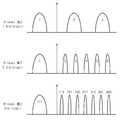
Translated fromKorean도 1 및 도 2는 플래시 메모리 셀의 문턱 전압 분포를 보여주는 도면;1 and 2 show threshold voltage distributions of flash memory cells;
도 3은 본 발명에 따른 플래시 메모리 장치의 메모리 셀 어레이의 구성을 보여주는 블록도;3 is a block diagram showing a configuration of a memory cell array of a flash memory device according to the present invention;
도 4는 도 3에 도시된 낸드 스트링을 구성하는 메모리 셀들의 구성 예를 보여주는 도면;4 is a diagram illustrating a configuration example of memory cells constituting the NAND string shown in FIG. 3;
도 5 및 도 6은 본 발명에 따른 플래시 메모리 장치의 비트 가변 예를 보여주는 도면;5 and 6 show examples of bit variation of a flash memory device according to the present invention;
도 7은 본 발명의 실시예에 따른 플래시 메모리 장치의 구성을 보여주는 블록도;7 is a block diagram showing a configuration of a flash memory device according to an embodiment of the present invention;
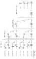
도 8은 도 7에 도시되어 있는 페이지 버퍼(PB)의 개략적인 구성을 보여주는 블록도;8 is a block diagram showing a schematic configuration of the page buffer PB shown in FIG.
도 9는 도 7에 도시되어 있는 페이지 버퍼(PB)의 상세 구성을 보여주는 회로도;9 is a circuit diagram showing a detailed configuration of a page buffer PB shown in FIG.
도 10은 도 7 내지 도 9에 도시된 페이지 버퍼(PB)에 구비된 제 1 및 제 2 래치에 할당된 기능을 보여주는 도면;FIG. 10 is a view showing functions allocated to first and second latches provided in the page buffer PB shown in FIGS. 7 to 9;
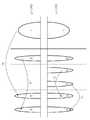
도 11은 하나의 메모리 셀에 2.5 비트(즉, 6 레벨)의 데이터가 저장되는 경 우(즉, 두 개의 메모리 셀에 5 비트의 데이터가 저장되는 경우)의 플래시 메모리 셀의 문턱 전압 분포를 보여주는 도면;FIG. 11 shows the threshold voltage distribution of a flash memory cell when 2.5 bits (ie, 6 levels) of data are stored in one memory cell (ie, when 5 bits of data are stored in two memory cells). drawing;
도 12는 6 레벨 MLC 프로그램의 4번째 프로그램에 대응되는 문턱 전압의 변화를 보여주는 도면;12 is a view showing a change in threshold voltage corresponding to the fourth program of the six-level MLC program;
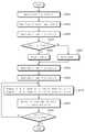
도 13은 6 레벨 MLC 프로그램의 4번째 프로그램 방법을 보여주는 흐름도;13 is a flowchart showing a fourth program method of a six-level MLC program;
도 14는 본 발명의 다른 실시예에 따른 플래시 메모리 장치의 구성을 보여주는 블록도;14 is a block diagram showing a configuration of a flash memory device according to another embodiment of the present invention;
도 15는 도 14에 도시되어 있는 페이지 버퍼(PB')의 개략적인 구성을 보여주는 블록도;FIG. 15 is a block diagram showing a schematic configuration of the page buffer PB 'shown in FIG.
도 16는 도 14에 도시되어 있는 페이지 버퍼(PB')의 상세 구성을 보여주는 회로도;FIG. 16 is a circuit diagram showing a detailed configuration of the page buffer PB 'shown in FIG.
도 17은 도 14 내지 도 16에 도시된 페이지 버퍼(PB')에 구비된 제 1 내지 제 3 래치에 할당된 기능을 보여주는 도면;FIG. 17 is a view showing functions allocated to first to third latches provided in the page buffer PB 'shown in FIGS. 14 to 16;
도 18은 6 레벨 MLC 프로그램의 4번째 프로그램에 대응되는 문턱 전압의 변화를 보여주는 도면; 그리고18 is a view showing a change in threshold voltage corresponding to the fourth program of the six-level MLC program; And
도 19는 6 레벨 MLC 프로그램의 4번째 프로그램 방법을 보여주는 흐름도이다.19 is a flowchart showing a fourth program method of a six-level MLC program.
* 도면의 주요 부분에 대한 부호 설명 *Explanation of symbols on the main parts of the drawings
51-53 : 래치100 : 플래시 메모리 장치51-53: Latch 100: Flash Memory Device
120 : 메모리 셀 어레이130 : 행 디코더120: memory cell array 130: row decoder
140 : 비트라인 선택 및 바이어스 회로140: bit line selection and bias circuit
150, 250 : 페이지 버퍼 회로150, 250: page buffer circuit
180 : 페이지 버퍼 디코더180: page buffer decoder
190 : 제어 로직190: control logic
본 발명은 반도체 메모리 장치에 관한 것으로, 좀 더 구체적으로는 하나의 메모리 셀에 멀티 비트 데이터를 저장할 수 있는 멀티 비트 플래시 메모리 장치에 관한 것이다.The present invention relates to a semiconductor memory device, and more particularly, to a multi-bit flash memory device capable of storing multi-bit data in one memory cell.
반도체 메모리 장치는 크게 휘발성 반도체 메모리 장치(volatile semiconductor memory device)와 불 휘발성 반도체 메모리 장치(non-volatile semiconductor memory device)로 구분된다. 휘발성 반도체 메모리 장치는 읽고 쓰는 속도가 빠르지만 외부 전원 공급이 끊기면 저장된 내용이 사라져 버리는 단점이 있다. 반면에 불 휘발성 반도체 메모리 장치는 외부 전원 공급이 중단되더라도 그 내용을 보존한다. 그러므로, 불 휘발성 반도체 메모리 장치는 전원이 공급되었는지의 여부에 관계없이 보존되어야 할 내용을 기억시키는 데 쓰인다. 불 휘발성 반도체 메모리 장치로는 마스크 롬(mask read-only memory, MROM), 프로그램 가능한 롬(programmable read-only memory, PROM), 소거 및 프로그램 가능한 롬(erasable programmable read-only memory, EPROM), 전기적으로 소거 및 프로그램 가능한 롬(electrically erasable programmable read-only memory, EEPROM) 등이 있다.Semiconductor memory devices are largely classified into volatile semiconductor memory devices and non-volatile semiconductor memory devices. The volatile semiconductor memory device has a high reading and writing speed, but the stored content disappears when the external power supply is cut off. On the other hand, nonvolatile semiconductor memory devices retain their contents even when the external power supply is interrupted. Therefore, the nonvolatile semiconductor memory device is used to store contents to be preserved regardless of whether or not power is supplied. Nonvolatile semiconductor memory devices include mask read-only memory (MROM), programmable read-only memory (PROM), erasable and programmable programmable read-only memory (EPROM), electrically Electrically erasable programmable read-only memory (EEPROM).
일반적으로, MROM, PROM 및 EPROM은 시스템 자체적으로 소거 및 쓰기가 자유롭지 않아서 일반 사용자들이 기억 내용을 갱신하기가 용이하지 않다. 이에 반해 EEPROM은 전기적으로 소거 및 쓰기가 가능하기 때문에, 계속적인 갱신이 필요한 시스템 프로그래밍(system programming)이나 보조 기억 장치로의 응용이 확대되고 있다. 특히 플래시(flash) EEPROM(이하, '플래시 메모리'라 칭함)은 기존의 EEPROM에 비해 집적도가 높아, 대용량 보조 기억 장치로의 응용에 매우 유리하다. 플래시 메모리의 집적도를 향상시키는 기술로서, 한 개의 메모리 셀에 다수 비트들의 데이터를 저장하는 멀티 비트(multi-bit), 멀티 레벨(multi-level), 또는 멀티 스테이트(multi-state) 플래시 메모리에 대한 연구가 활발히 진행되고 있다.In general, MROMs, PROMs, and EPROMs are not free to erase and write on the system itself, making it difficult for ordinary users to update their contents. On the other hand, since EEPROMs can be electrically erased and written, applications to system programming or auxiliary storage devices requiring continuous updating are expanding. In particular, flash EEPROM (hereinafter referred to as "flash memory") has a higher density than conventional EEPROM, which is very advantageous for application to a large capacity auxiliary storage device. A technique for improving the density of flash memory, a technique for multi-bit, multi-level, or multi-state flash memory that stores multiple bits of data in one memory cell. Research is actively underway.
대용량 기억 장치에서 요구되는 가장 중요한 요건은, 낮은 비트당 가격(low cost per bit)을 구현하는 것이다. 이와 같은 요구에 따라, 플래시 메모리 장치의 비트당 가격을 획기적으로 줄일 수 있는 기술이 1995년 2월, M. Bauer 등에 의해 IEEE, ISSCC Digest of Technical Papers, pp. 132-133에, "A Multilevel-Cell 32Mb Flash Memory"라는 제목으로 게재(揭載)된 바 있다. 상기 문헌에 개시(開示)된 플래시 메모리 장치는 NOR 구조의 셀 어레이를 가지는 장치이며, 셀 크기의 감소와 더불어 1개의 셀 당 2 비트, 즉 4 레벨의 데이터가 저장된다. 상기 플래시 메모리 장치에 저장되는 데이터 상태들을 2 진법으로 나타내면, "00", "01", "10", "11"이 된다. 각각의 데이터 상태(00, 01, 10, 11)에는 특정한 문턱 전압 레벨(threshold voltage level)이 각각 부여된다. 각 메모리 셀이 상기 4 레벨들에 대응되는 문턱 전압들 중 하나의 문턱 전압 레벨을 가짐에 의해서, 상기 데이터 상태들(11, 10, 01, 00) 중 하나의 데이터 상태가 각 메모리 셀에 저장된다. 여기서, 각각의 데이터 상태에 대응되는 문턱 전압의 분포와 각각의 메모리 셀에 저장 가능한 비트 수는 다양한 형태로 변경 및 변형될 수 있다.The most important requirement for mass storage devices is the implementation of low cost per bit. In response to such demands, a technology that can drastically reduce the price per bit of a flash memory device has been described by IEEE, ISSCC Digest of Technical Papers, pp. 132-133, entitled "A Multilevel-Cell 32Mb Flash Memory." The flash memory device disclosed in this document is a device having a cell array having a NOR structure and stores two bits, or four levels of data, per cell with a decrease in cell size. When data states stored in the flash memory device are represented in binary format, they are “00”, “01”, “10”, and “11”. Each data state (00, 01, 10, 11) is given a specific threshold voltage level, respectively. As each memory cell has a threshold voltage level of one of the threshold voltages corresponding to the four levels, the data state of one of the
도 1 및 도 2는 플래시 메모리 셀의 문턱 전압 분포를 보여주는 도면으로, 각각의 메모리 셀에 저장될 수 있는 데이터 상태들의 예가 도시되어 있다.1 and 2 show threshold voltage distributions of flash memory cells, and examples of data states that may be stored in each memory cell are shown.
먼저 도 1을 참조하면, 하나의 플래시 메모리 셀에는 2n비트의 데이터, 예를 들면 1 비트(2 레벨 SLC(Single Level Cell)), 2 비트(4 레벨 MLC(Multi Level Cell)), 4 비트(16 레벨 MLC) 등의 데이터가 저장될 수 있다. 그러나, 상기 플래시 메모리 셀에는 2n비트뿐만 아니라 2n비트가 아닌 데이터도 저장될 수 있다. 2n비트가 아닌 데이터가 저장되는 예는 도 2와 같다. 도 2를 참조하면, 하나의 플래시 메모리 셀는 1.5 비트(3 레벨 SLC), 2.5 비트(6 레벨 MLC),3 비트(8 레벨 MLC) 등의 데이터가 저장될 수 있다.Referring first to FIG. 1, one flash memory cell has 2n bits of data, for example, 1 bit (2-level single level cell), 2 bit (4-level multi level cell), 4 bit Data such as (16 level MLC) may be stored. However, the flash memory cells, there can be stored the data other than 2n bits, as well as 2n bits. An example in which data other than 2n bits is stored is shown in FIG. 2. Referring to FIG. 2, one flash memory cell may store data such as 1.5 bits (3 level SLC), 2.5 bits (6 level MLC), 3 bits (8 level MLC), and the like.
멀티 비트 플래시 메모리에서, 인접한 상태들 사이의 윈도우(stage-to-state window)는 단일 비트 플래시 메모리 장치(single bit flash memory device)의 윈도우에 비해 그 폭이 좁다. 그리고, 독출 동작 동안에 선택된 워드 라인(selected word line)에 인가되는 전압과 문턱 전압 분포의 가장자리(edge) 간의 마진(margin)은, 윈도우 폭이 좁아짐에 따라 더욱 좁아지게 된다. 따라서, 멀티 비트 셀 어레이의 경우, 공정 변화(process variation)나 선택된 워드 라인의 전압 레 벨, 동작 전압, 온도 등의 변화에 의한 무효 감지(invalid sensing)의 가능성이 단일 비트 플래시 메모리 장치에서보다 더 높다. 그러므로, 바이오스(basic input/output system; BIOS) 정보, 폰트(font) 정보 등과 같이 우수한 보존 특성(storage characteristic)이 요구되는 정보들의 저장 장치로는 단일 비트 플래시 메모리가 유리하다. 반면에, 다량의 연속적인 정보들 중 한 개 비트 혹은 몇 개 비트 정보들의 저장 실패(storage failure)가 발생 된다 하더라도 큰 문제가 없는 정보들, 예를 들면 음성 정보 등의 저장 장치로는 멀티 비트 플래시 메모리가 유리하다.In multi-bit flash memory, the stage-to-state window is narrower than the window of a single bit flash memory device. And, the margin between the voltage applied to the selected word line and the edge of the threshold voltage distribution during the read operation becomes narrower as the window width becomes narrower. Therefore, in the case of a multi-bit cell array, the possibility of invalid sensing due to process variations or changes in the selected word line's voltage level, operating voltage, temperature, etc. is more than in a single bit flash memory device. high. Therefore, a single bit flash memory is advantageous as a storage device for information requiring excellent storage characteristics such as basic input / output system (BIOS) information, font information, and the like. On the other hand, even if a storage failure of one bit or a few bits of a large amount of continuous information occurs, the storage device such as information such as voice information, which is not a big problem, is used for multi-bit flash. Memory is advantageous.
플래시 메모리의 응용이 다양해짐에 따라, 단일 비트 플래시 메모리의 특성과 멀티 비트 플래시 메모리의 특성이 적절한 비율로 요구되는 경우가 자주 발생 된다. 종래에는, 대부분의 플래시 메모리 장치가 단일 비트 메모리 칩(single bit memory chip)과 멀티 비트 메모리 칩(multibit memory chip) 중 어느 하나의 타입으로 각각 별도로 구성되었다. 이에 따라, 메모리 칩에 대한 데이터의 프로그램, 독출, 및 소거 동작을 수행하는 페이지 버퍼의 구성 또한 단일 비트 메모리용 페이지 버퍼와 멀티 비트 메모리용 페이지 버퍼로 각각 별도로 구성되었다.As the application of the flash memory is diversified, the characteristics of the single bit flash memory and the characteristics of the multi bit flash memory are often required at an appropriate ratio. In the related art, most flash memory devices are separately configured as any one type of a single bit memory chip and a multibit memory chip. Accordingly, a page buffer for programming, reading, and erasing data to and from a memory chip is also separately configured as a page buffer for a single bit memory and a page buffer for a multi bit memory.
최근 들어서는 단일 메모리 셀 어레이 내에 단일 비트 메모리 셀과 멀티 비트 메모리 셀(또는, 서로 다른 비트를 저장하는 멀티 비트 메모리 셀)이 혼합된 플래시 메모리 장치가 개발되고 있다. 그리고, 퓨즈와 같은 스위칭 수단을 이용하여 하나의 메모리 셀을 단일 비트 메모리 셀로 스위칭하여 사용하거나 또는 멀티 비트 메모리 셀로 스위칭하여 사용할 수 있는 플래시 메모리 장치가 개발되고 있다. 하 지만, 이상과 같은 새로운 타입의 플래시 메모리 장치가 제공됨에도 불구하고, 페이지 버퍼의 구성은 단일 비트 플래시 메모리용 페이지 버퍼와 멀티 비트 플래시 메모리용 페이지 버퍼가 각각 별도로 구성된다. 따라서, 단일 메모리 셀 어레이 내에 단일 비트 메모리 셀과 멀티 비트 메모리 셀이 혼합된 플래시 메모리 장치, 또는 셀당 저장되는 비트 수가 가변되는 플래시 메모리 장치에는 단일 비트 플래시 메모리용 페이지 버퍼와 멀티 비트 플래시 메모리용 페이지 버퍼가 모두 구비되어야 하는 문제점이 있다. 이와 같은 문제점은 칩의 사이즈를 증가시키는 원인이 된다.Recently, flash memory devices in which a single bit memory cell and a multi bit memory cell (or a multi bit memory cell storing different bits) are mixed in a single memory cell array have been developed. In addition, a flash memory device capable of switching one memory cell to a single bit memory cell or switching to a multi-bit memory cell using a switching means such as a fuse has been developed. However, despite the above-described new type of flash memory device, the page buffer is composed of a page buffer for a single bit flash memory and a page buffer for a multi bit flash memory. Therefore, a flash memory device in which a single-bit memory cell and a multi-bit memory cell are mixed in a single memory cell array, or a flash memory device in which the number of bits stored per cell is variable, is a page buffer for a single bit flash memory and a page buffer for a multi-bit flash memory. There is a problem that all should be provided. This problem is a cause of increasing the size of the chip.
따라서, 본 발명의 목적은 상술한 제반 문제점을 해결하기 위해 제안된 것으로, 다양한 종류의 멀티 비트 셀에 적용 가능한 페이지 버퍼를 구비한 플래시 메모리 장치를 제공하는 데 있다.Accordingly, an object of the present invention is to solve the above-mentioned problems and to provide a flash memory device having a page buffer applicable to various types of multi-bit cells.
본 발명의 다른 목적은 메모리 셀에 저장되는 비트 수가 달라지더라도 달라진 비트 수에 대응되는 프로그램 및 기입 동작을 유동적으로 수행할 수 있는 플래시 메모리 장치를 제공하는 데 있다.Another object of the present invention is to provide a flash memory device capable of flexibly performing program and write operations corresponding to the changed number of bits even if the number of bits stored in the memory cell is different.
본 발명의 또 다른 목적은 칩 사이즈를 줄일 수 있는 플래시 메모리 장치를 제공하는 데 있다.Still another object of the present invention is to provide a flash memory device capable of reducing chip size.
상술한 제반 목적을 달성하기 위한 본 발명의 일 특징에 따르면, 플래시 메모리 장치는 셀 당 저장되는 비트 수를 변경할 수 있는 메모리 셀들의 어레이; 복 수 개의 페이지 버퍼들로 구성되어, 상기 메모리 셀들에 대한 프로그램, 독출, 또는 소거 동작을 수행하는 페이지 버퍼 회로; 그리고 상기 셀 당 저장되는 비트 수에 따라 상기 각각의 페이지 버퍼의 동작을 제어하는 제어 로직을 포함하며, 상기 각각의 페이지 버퍼는, 상기 셀 당 저장되는 비트 수에 따라서 각각에 저장될 데이터가 정의되는 복수 개의 래치들을 포함하는 것을 특징으로 한다.According to one aspect of the present invention for achieving the above object, a flash memory device comprises an array of memory cells that can change the number of bits stored per cell; A page buffer circuit including a plurality of page buffers to perform a program, read, or erase operation on the memory cells; And control logic for controlling the operation of each page buffer according to the number of bits stored per cell, wherein each page buffer has data defined to be stored in each according to the number of bits stored per cell. It characterized in that it comprises a plurality of latches.
이 실시예에 있어서, 상기 각각의 래치는 상기 제어 블록의 제어에 응답해서 상기 메모리 셀들과 선택적으로 연결되는 것을 특징으로 한다.In this embodiment, each latch is selectively connected with the memory cells in response to the control of the control block.
이 실시예에 있어서, 상기 래치들은 독립적인 인터페이스를 수행하는 것을 특징으로 한다.In this embodiment, the latches are characterized in that they perform independent interfaces.
이 실시예에 있어서, 상기 각각의 페이지 버퍼는 상기 셀 당 저장되는 비트 수에 따라서 각각이 수행할 데이터 저장 기능이 가변되는 제 1 및 제 2 래치를 포함하는 것을 특징으로 한다.In this embodiment, each of the page buffers may include first and second latches whose data storage functions vary according to the number of bits stored per cell.
이 실시예에 있어서, 상기 메모리 셀 당 1 비트의 데이터가 저장되는 경우, 상기 제 1 래치는 선택된 메모리 셀에 대한 프로그램 데이터 및 독출 데이터를 저장하고, 상기 제 2 래치는 상기 프로그램 데이터를 상기 제 1 래치로 전달하는 캐쉬로서의 기능을 수행하는 것을 특징으로 한다.In this embodiment, when one bit of data is stored per memory cell, the first latch stores program data and read data for a selected memory cell, and the second latch stores the program data in the first It performs a function as a cache for transferring to the latch.
이 실시예에 있어서, 상기 메모리 셀 당 1.5 비트의 데이터가 저장되는 경우, 상기 제 1 래치는 선택된 제 1 메모리 셀에 대한 프로그램 데이터 및 독출 데이터를 저장하고, 상기 제 2 래치는 선택된 제 2 메모리 셀에 대한 프로그램 데이터 및 독출 데이터를 각각 저장하는 것을 특징으로 한다.In this embodiment, when 1.5 bits of data are stored per memory cell, the first latch stores program data and read data for the selected first memory cell, and the second latch stores the selected second memory cell. Program data and read data for each of the characterized in that it stores.
이 실시예에 있어서, 상기 메모리 셀 당 2 비트의 데이터가 저장되는 경우, 상기 제 1 래치는 선택된 메모리 셀에 대한 프로그램 데이터 및 독출 데이터를 저장하고, 상기 제 2 래치는 상기 제 1 래치에 저장되어 있는 데이터가 프로그램되기 이전에 상기 선택된 메모리 셀에 프로그램되어 있는 데이터를 독출하여 저장하는 것을 특징으로 한다.In this embodiment, when two bits of data are stored per memory cell, the first latch stores program data and read data for a selected memory cell, and the second latch is stored in the first latch. The data programmed in the selected memory cell may be read and stored before the existing data is programmed.
이 실시예에 있어서, 상기 메모리 셀 당 2.5 비트의 데이터가 저장되는 경우, 상기 제 1 래치는 제 1 메모리 셀 및 제 2 메모리 셀 중 어느 하나에 대한 프로그램 데이터 및 독출 데이터를 저장하고, 상기 제 2 래치는 상기 제 1 래치에 저장되어 있는 데이터가 프로그램되기 이전에 상기 제 1 메모리 셀 및 상기 제 2 메모리 셀 중 선택된 어느 하나에 프로그램되어 있는 데이터를 독출하여 저장하는 것을 특징으로 한다.In this embodiment, when 2.5 bits of data are stored per memory cell, the first latch stores program data and read data for either one of a first memory cell and a second memory cell, and the second latch. The latch reads and stores data programmed in any one selected from the first memory cell and the second memory cell before the data stored in the first latch is programmed.
이 실시예에 있어서, 상기 메모리 셀 당 3 비트의 데이터가 저장되는 경우, 상기 제 1 래치는 선택된 메모리 셀에 대한 프로그램 데이터 및 독출 데이터를 저장하고, 상기 제 2 래치는 상기 제 1 래치에 저장되어 있는 데이터가 프로그램되기 이전에 상기 선택된 메모리 셀에 프로그램되어 있는 데이터를 독출하여 저장하는 것을 특징으로 한다.In this embodiment, when 3 bits of data are stored per memory cell, the first latch stores program data and read data for a selected memory cell, and the second latch is stored in the first latch. The data programmed in the selected memory cell may be read and stored before the existing data is programmed.
이 실시예에 있어서, 상기 메모리 셀 당 2n 비트의 데이터가 저장되는 경우, 상기 제 1 래치는 선택된 메모리 셀에 대한 프로그램 데이터 및 독출 데이터를 저장하고, 상기 제 2 래치는 상기 제 1 래치에 저장되어 있는 데이터가 프로그램되기 이전에 상기 선택된 메모리 셀에 프로그램되어 있는 데이터를 독출하여 저장하는 것을 특징으로 한다.In this embodiment, when 2n bits of data are stored per memory cell, the first latch stores program data and read data for the selected memory cell, and the second latch is stored in the first latch. The data programmed in the selected memory cell is read and stored before the data is programmed.
이 실시예에 있어서, 상기 각각의 페이지 버퍼는 상기 셀 당 저장되는 비트 수에 따라서 각각이 수행할 데이터 저장 기능이 가변되는 제 1 내지 제 3 래치를 포함하는 것을 특징으로 한다.In the present embodiment, each page buffer may include first to third latches whose data storage functions vary according to the number of bits stored per cell.
이 실시예에 있어서, 상기 메모리 셀 당 1 비트의 데이터가 저장되는 경우, 상기 제 1 래치는 선택된 메모리 셀에 대한 프로그램 데이터 및 독출 데이터를 저장하고, 상기 제 2 래치는 상기 프로그램 데이터를 상기 제 1 래치로 전달하는 캐쉬로서의 기능을 수행하는 것을 특징으로 한다.In this embodiment, when one bit of data is stored per memory cell, the first latch stores program data and read data for a selected memory cell, and the second latch stores the program data in the first It performs a function as a cache for transferring to the latch.
이 실시예에 있어서, 상기 메모리 셀 당 1.5 비트의 데이터가 저장되는 경우, 상기 제 1 래치는 선택된 제 1 메모리 셀에 대한 프로그램 데이터 및 독출 데이터를 저장하고, 상기 제 2 래치는 선택된 제 2 메모리 셀에 대한 프로그램 데이터 및 독출 데이터를 저장하고, 상기 제 3 래치는 상기 프로그램 데이터들을 상기 제 1 및 제 2 래치로 각각 전달하는 캐쉬로서의 기능을 수행하는 것을 특징으로 한다.In this embodiment, when 1.5 bits of data are stored per memory cell, the first latch stores program data and read data for the selected first memory cell, and the second latch stores the selected second memory cell. Stores program data and read data for the third latch, and the third latch performs a function as a cache for transferring the program data to the first and second latches, respectively.
이 실시예에 있어서, 상기 메모리 셀 당 2 비트의 데이터가 저장되는 경우, 상기 제 1 래치는 선택된 메모리 셀에 대한 프로그램 데이터 및 독출 데이터를 저장하고, 상기 제 2 래치는 상기 제 1 래치에 저장되어 있는 데이터가 프로그램되기 이전에 상기 선택된 메모리 셀에 프로그램되어 있는 데이터를 독출하여 저장하고, 상기 제 3 래치는 상기 프로그램 데이터를 상기 제 1 래치로 전달하는 캐쉬로서의 기능을 수행하는 것을 특징으로 한다.In this embodiment, when two bits of data are stored per memory cell, the first latch stores program data and read data for a selected memory cell, and the second latch is stored in the first latch. Read and store data programmed in the selected memory cell before the existing data is programmed, and the third latch performs a function as a cache for transferring the program data to the first latch.
이 실시예에 있어서, 상기 메모리 셀 당 2.5 비트의 데이터가 저장되는 경우, 상기 제 1 래치는 선택된 제 1 메모리 셀에 대한 프로그램 데이터 및 독출 데이터를 저장하고, 상기 제 2 래치는 선택된 제 2 메모리 셀에 대한 프로그램 데이터 및 독출 데이터를 저장하고, 상기 제 3 래치는 상기 제 1 및 제 2 래치에 저장되어 있는 상기 프로그램 데이터들을 구분하기 위한 제 3 데이터를 저장하는 것을 특징으로 한다.In this embodiment, when 2.5 bits of data are stored per memory cell, the first latch stores program data and read data for the selected first memory cell, and the second latch stores the selected second memory cell. Program data and read data for the third latch; and the third latch stores third data for distinguishing the program data stored in the first and second latches.
이 실시예에 있어서, 상기 메모리 셀 당 3 비트의 데이터가 저장되는 경우, 상기 제 1 래치는 선택된 메모리 셀에 대한 프로그램 데이터 및 독출 데이터를 저장하고, 상기 제 2 래치는 상기 제 1 래치에 저장되어 있는 데이터가 프로그램되기 이전에 상기 선택된 메모리 셀에 프로그램되어 있는 데이터를 독출하여 저장하고, 상기 제 3 래치는 상기 프로그램 데이터를 상기 제 1 래치로 전달하는 캐쉬로서의 기능을 수행하는 것을 특징으로 한다.In this embodiment, when 3 bits of data are stored per memory cell, the first latch stores program data and read data for a selected memory cell, and the second latch is stored in the first latch. Read and store data programmed in the selected memory cell before the existing data is programmed, and the third latch performs a function as a cache for transferring the program data to the first latch.
이 실시예에 있어서, 상기 메모리 셀 당 2n 비트의 데이터가 저장되는 경우, 상기 제 1 래치는 선택된 메모리 셀에 대한 프로그램 데이터 및 독출 데이터를 저장하고, 상기 제 2 래치는 상기 제 1 래치에 저장되어 있는 데이터가 프로그램되기 이전에 상기 선택된 메모리 셀에 프로그램되어 있는 데이터를 독출하여 저장하고, 상기 제 3 래치는 상기 프로그램 데이터를 상기 제 1 래치로 전달하는 캐쉬로서의 기능을 수행하는 것을 특징으로 한다.In this embodiment, when 2n bits of data are stored per memory cell, the first latch stores program data and read data for the selected memory cell, and the second latch is stored in the first latch. Read and store data programmed in the selected memory cell before the programmed data is programmed, and the third latch performs a function of a cache for transferring the program data to the first latch.
이 실시예에 있어서, 상기 셀 당 저장되는 비트 수는 퓨징 옵션 및 레지스터 세팅 중 어느 하나의 방식에 의해 설정되는 것을 특징으로 한다.In this embodiment, the number of bits stored per cell is set by one of a fusing option and a register setting.
이 실시예에 있어서, 상기 메모리 셀 어레이는, 소정의 페이지로 할당된 복수 개의 메모리 블록들을 포함하며, 적어도 하나 이상의 메모리 블록 단위로 상기 셀 당 저장되는 비트 수가 변경되는 것을 특징으로 한다.In this embodiment, the memory cell array includes a plurality of memory blocks allocated to a predetermined page, and the number of bits stored per cell is changed in units of at least one memory block.
이 실시예에 있어서, 상기 각각의 블록에 배선된 각각의 비트라인에는 셀 당 저장되는 비트 수가 서로 다른 적어도 둘 이상의 메모리 셀들이 접속되는 것을 특징으로 한다.In this embodiment, at least two or more memory cells having different numbers of bits stored per cell are connected to each bit line wired to each block.
이 실시예에 있어서, 상기 각각의 블록에는 2n개의 페이지가 할당되는 것을 특징으로 한다.In this embodiment, 2n pages are allocated to each block.
이 실시예에 있어서, 상기 비트라인에는 2n 비트의 데이터를 저장하는 메모리 셀이 접속되는 것을 특징으로 한다.In this embodiment, a memory cell for storing data of 2n bits is connected to the bit line.
이 실시예에 있어서, 상기 비트라인에는 2n 비트가 아닌 데이터를 저장하는 메모리 셀이 접속되는 것을 특징으로 한다.In this embodiment, a memory cell storing data other than 2n bits is connected to the bit line.
이 실시예에 있어서, 상기 비트라인에는 데이터를 저장하지 않는 더미 셀이 접속되는 것을 특징으로 한다.In this embodiment, a dummy cell which does not store data is connected to the bit line.
이 실시예에 있어서, 상기 블록에 할당되는 페이지의 개수가 2n 개를 만족시키는 범위 내에서 상기 각각의 비트라인에 접속되는 메모리 셀의 개수가 가변되는 것을 특징으로 한다.In this embodiment, the number of memory cells connected to each of the bit lines is variable within a range in which the number of pages allocated to the block satisfies 2n .
이 실시예에 있어서, 상기 블록에 배선된 상기 비트라인에 접속되는 메모리 셀의 개수가 2n 개인 경우, 대응되는 블록의 페이지 개수는 2n 개의 범위를 벗어나 상기 각각의 메모리 셀에 저장되는 비트 수에 따라 가변되는 것을 특징으로 한다.In this embodiment, when the number of memory cells connected to the bit line wired to the block is 2n , the number of pages of the corresponding block is out of the range of 2n and the number of bits stored in each memory cell. It is characterized by varying according to.
이 실시예에 있어서, 상기 각각의 비트라인에 접속되는 상기 메모리 셀의 종류 및 상기 메모리 셀의 개수는 상기 각각의 블록마다 다른 것을 특징으로 한다.In this embodiment, the type of the memory cells connected to the respective bit lines and the number of the memory cells are different for each block.
이 실시예에 있어서, 상기 각각의 비트라인에 접속되는 상기 메모리 셀의 종류 및 상기 메모리 셀의 개수는 상기 각각의 블록마다 동일한 것을 특징으로 한다.In this embodiment, the type of the memory cells and the number of the memory cells connected to the respective bit lines are the same for each of the blocks.
이 실시예에 있어서, 상기 메모리 셀들은 낸드형 플래시 메모리 셀인 것을 특징으로 한다.In this embodiment, the memory cells are NAND type flash memory cells.
이 실시예에 있어서, 상기 메모리 셀들은 노어형 플래시 메모리 셀인 것을 특징으로 한다.In this embodiment, the memory cells are NOR flash memory cells.
(실시예)(Example)
이하 본 발명에 따른 실시예를 첨부된 도면을 참조하여 상세히 설명한다.Hereinafter, exemplary embodiments of the present invention will be described in detail with reference to the accompanying drawings.
본 발명의 신규한 플래시 메모리 장치에 포함된 메모리 셀들의 데이터 저장 특성은 사용자의 요구에 따라 다양한 형태로 변경될 수 있다. 각각의 메모리 셀들에 대한 데이터 저장 특성은 퓨징 옵션, 레지스터 세팅 등의 방식으로 설정된다. 제어 로직(control logic)은 상기 설정된 각각의 메모리 셀들에 대한 데이터 저장 특성에 응답해서, 페이지 버퍼의 각각의 래치에서 수행되는 기능을 각각 유동적으 로 설정한다. 그 결과, 각각의 메모리 셀에 저장되는 비트 수가 달라지더라도 페이지 버퍼의 구조가 달라지지 않고 해당 메모리 셀에 대한 프로그램, 독출, 및 소거 동작을 모두 수행할 수 있게 된다.Data storage characteristics of the memory cells included in the novel flash memory device of the present invention may be changed in various forms according to a user's request. The data storage characteristic for each memory cell is set in the manner of fusing option, register setting, and so on. Control logic fluidly sets the function to be performed at each latch of the page buffer in response to the data storage characteristic for each of the memory cells set above. As a result, even if the number of bits stored in each memory cell is different, the structure of the page buffer is not changed, and all of the program, read, and erase operations for the corresponding memory cell can be performed.
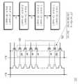
도 3은 본 발명에 따른 플래시 메모리 장치의 메모리 셀 어레이(120)의 구성을 보여주는 블록도이다. 그리고, 도 4는 도 3에 도시된 낸드 스트링을 구성하는 메모리 셀들의 구성 예를 보여주는 도면이다. 도 3 및 도 4에는 적어도 두 종류 이상의 메모리 셀(즉, 서로 다른 비트를 저장하는 적어도 두 종류 이상의 메모리 셀)로 구성된 낸드형 멀티-비트 플래시 메모리 장치의 구성이 예시적으로 도시되어 있다. 아래에서는 본 발명이 적용되는 일 예로서 낸드형 플래시 메모리 장치가 예를 들어 설명될 것이다. 그러나, 이는 본 발명이 적용되는 일 예에 불과하며, 다양한 형태로 변형 및 변경 가능하다. 예를 들면, 본 발명에서는 낸드형 플래시 메모리 장치에 대해 설명하고 있지만, 본 발명이 가지고 있는 구성상의 특징은 노어형 플래시 메모리 장치에도 적용 가능하다.3 is a block diagram illustrating a configuration of a
도 3 및 도 4를 참조하면, 메모리 셀 어레이(120)에는 복수 개의 블록들(BK1-BKn)이 포함된다. 각각의 블록(BK1-BKn)은 32, 64, 128, 또는 256 개의 페이지들로 구성되며, 하나의 페이지는 512B의 크기를 갖는다.3 and 4, the
상기 블록들(BK1-BKn) 중 한 블록(121)의 물리적인 구조를 살펴보면, 하나의 블록(121)에는 비트라인 방향으로 배열된 복수 개의 낸드 스트링들이 포함된다. 각각의 낸드 스트링에는 22, 23, 43, 44, 45, 52, … 개의 메모리 셀들이 포함된다. 각각의 낸드 스트링에 포함된 메모리 셀들은 바람직하게는 셀 당 저장되는 비트 수가 다른 적어도 두 종류 이상의 메모리 셀들(M1, M2, M3)로 구성된다. 본 발명에서는 적어도 둘 이상의 이종(異種) 메모리 셀들이 구비된 스트링을 복합형 낸드 스트링이라 부르기로 한다. 그리고, 상기 복합형 낸드 스트링들로 구성된 메모리 셀 어레이를 복합형 메모리 셀 어레이라 부르기로 한다.Looking at the physical structure of one
낸드형 플래시 메모리의 프로그램 또는 독출 동작은 페이지 단위로 수행되며, 프로그램된 데이터의 소거 동작은 페이지가 여러 개 모인 단위인 블록 단위로 수행된다. 따라서, 각각의 블록에 할당되는 페이지의 개수는 플래시 메모리의 동작을 제어함에 있어서 매우 중요하다. 이 분야의 통상의 지식을 가진 이들에게 잘 알려져 있는 바와 같이, 대부분의 플래시 메모리 장치 제조 업체들은 단위 메모리 셀에 2n 비트가 저장되는 경우를 기준으로 하여 제품을 생산하고 있다. 이에 따라, 플래시 메모리 장치의 제품 스펙들과 파일 시스템의 제어 방식들 또한 단위 메모리 셀에 2n 비트가 저장되는 메모리 셀을 기준으로 정의되고 있다. 그러므로, 각각의 블록에 할당되는 페이지의 개수가 2의 멱지수 형태(즉, 2n 형태)이어야만 기존의 제어 방식을 그대로 적용할 수 있다. 특히, 셀 당 저장되는 비트 수가 가변되거나 또는 다양한 종류의 메모리 셀들이 하나의 낸드 스트링에 포함될 경우, 각각의 블록에 할당되는 페이지의 개수가 기존의 스펙에 정의되어 있는 것과 달라지지 않도록 하는 것이 바람직하다. 이와 같은 이유로 인해, 도 3에 도시된 낸드 스트링은 해당 블록에 할당되는 페이지 개수가 2의 멱지수 형태(즉, 2n 형태)가 될 수 있도록 메모리 셀의 개수를 조절한다. 이 경우, 상기 낸드 스트링에 포함된 메모리 셀의 개수는 2의 멱지수 형태(즉, 2n 형태)를 가지지는 않는다. 그러나, 이는 본 발명이 적용되는 일 예에 불과하며, 다양한 형태로 변경 및 변형 가능하다.The program or read operation of the NAND flash memory is performed in units of pages, and the erase operation of programmed data is performed in units of blocks, which are a unit of several pages. Therefore, the number of pages allocated to each block is very important in controlling the operation of the flash memory. As is well known to those of ordinary skill in the art, most flash memory device manufacturers produce products based on the case where 2n bits are stored in a unit memory cell. Accordingly, product specifications of the flash memory device and control methods of the file system are also defined based on a memory cell in which 2n bits are stored in a unit memory cell. Therefore, the existing control scheme can be applied as it is only when the number of pages allocated to each block is an exponential form of 2 (that is, 2n form). In particular, when the number of bits stored per cell is variable or various kinds of memory cells are included in one NAND string, it is desirable that the number of pages allocated to each block is not different from that defined in the existing specification. . For this reason, the NAND string shown in FIG. 3 adjusts the number of memory cells so that the number of pages allocated to the block may be an exponential form of 2 (that is, 2n form). In this case, the number of memory cells included in the NAND string does not have an exponential form of 2 (that is, 2n form). However, this is only an example to which the present invention is applied, and may be changed and modified in various forms.
도 3에서 M1으로 표시된 메모리 셀들은 1개의 메모리 셀 당 1.5 비트(또는, 2.5 비트 또는 3비트)가 저장되는 메모리 셀들로, 제 1 타입의 메모리 셀들로 정의된다. 제 1 타입의 메모리 셀들(M1)은 1개의 메모리 셀 당 2n비트가 아닌 데이터(예를 들면, 2n-1 비트의 데이터)가 저장된다. M2로 표시된 메모리 셀은 1개의 메모리 셀 당 1 비트(또는 2비트)가 저장되는 메모리 셀로서, 제 2 타입의 메모리 셀로 정의된다. 제 2 타입의 메모리 셀(M2)은 1개의 메모리 셀 당 2n 비트가 저장된다. 그리고, M3으로 표시된 메모리 셀은 데이터를 저장하지 않는 더미 셀로서, 제 3 타입의 메모리 셀로 정의된다. 각각의 복합형 낸드 스트링은 대부분의 메모리 셀들이 제 1 타입 메모리 셀들(M1)로 구성되고, 일부의 셀들이 제 2 또는 제 3 타입 메모리 셀로 구성된다. 제 2 또는 제 3 타입 메모리 셀(M2, M3)은, 스트링의 구조상 프로그램 특성 등이 취약한 위치에 배치될 수 있다.In FIG. 3, memory cells indicated as M1 are memory cells in which 1.5 bits (or 2.5 bits or 3 bits) are stored per memory cell, and are defined as memory cells of a first type. The first type of memory cells M1 store data (for example, 2n-1 bits of data) rather than 2n bits per memory cell. The memory cell indicated by M2 is a memory cell in which one bit (or two bits) is stored per memory cell, and is defined as a memory cell of a second type. The second type of memory
예를 들면, 도 4에 도시된 바와 같이, 1개의 블록이 64 페이지로 구성되고 1개의 복합형 낸드 스트링이 22개의 메모리 셀들로 구성되는 경우, 20개의 메모리 셀은 각각이 1.5 비트의 데이터를 저장하는 제 1 타입의 메모리 셀(M1)(즉, 3 레벨 SLC)로 구성될 수 있다. 그리고, 나머지 2개의 메모리 셀은 각각이 1 비트의 데이터를 저장하는 제 2 타입의 메모리 셀(M2)(즉, 2 레벨 SLC)로 구성될 수 있다. 이 경우, 제 2 타입의 메모리 셀(M2)은 스트링의 구조상 프로그램 특성 등이 취약한 스트링의 최하위 워드라인과 최상위 워드라인에 각각 배치될 수 있다.For example, as shown in FIG. 4, when one block consists of 64 pages and one complex NAND string consists of 22 memory cells, 20 memory cells each store 1.5 bits of data. It may be composed of a first type of memory cell M1 (that is, three-level SLC). The remaining two memory cells may be configured of a second type of memory cell M2 (that is, two level SLC), each of which stores one bit of data. In this case, the second type of memory cell M2 may be disposed on the lowest word line and the highest word line of the string, which are poor in program characteristics, etc., of the string.
플래시 메모리의 응용 분야가 다양해짐에 따라, 반도체 제조 업체에서는 메모리 셀에 저장될 수 있는 비트 수를 가변시킬 수 있는 플래시 메모리 장치를 제조하고 있다. 상기 메모리를 이용하여 어플리케이션을 개발하는 회사들은 해당 메모리의 사용 용도에 따라서 메모리 셀에 저장 가능한 비트 수를 다양하게 조절한다. 예를 들면, 높은 정확도를 요구하는 정보들을 저장하는 경우에는 메모리 셀에 저장되는 비트 수를 낮게(예를 들면, 1 비트, 1.5 비트 등) 조절한다. 그리고, 높은 정확도를 필요로 하지 않는 다량의 정보들을 저장하는 경우에는 메모리 셀에 저장되는 비트 수를 높게(예를 들면, 2 비트, 3 비트 등) 조절한다.As flash memory applications are diversified, semiconductor manufacturers are manufacturing flash memory devices that can vary the number of bits that can be stored in a memory cell. Companies that develop applications using the memory vary the number of bits that can be stored in the memory cell according to the use of the memory. For example, when storing information requiring high accuracy, the number of bits stored in the memory cell is adjusted low (for example, 1 bit, 1.5 bits, etc.). In the case of storing a large amount of information that does not require high accuracy, the number of bits stored in the memory cell is adjusted (for example, 2 bits, 3 bits, etc.).
아래에서 상세히 설명되겠지만, 본 발명에 따른 플래시 메모리 장치는 각각의 메모리 셀에 저장되는 비트 수가 달라지더라도 페이지 버퍼의 구조를 변경하지 않고 해당 메모리 셀에 대한 프로그램, 독출, 및 소거 동작을 모두 수행한다. 본 발명에 따른 플래시 메모리 장치는 블록 단위로 메모리 셀에 저장되는 비트 수를 조절할 수도 있고, 스트링 단위로 셀에 저장되는 비트 수를 조절할 수도 있으며, 워드라인 단위로 메모리 셀에 저장되는 비트 수를 조절할 수도 있다.As will be described in detail below, the flash memory device according to the present invention performs all program, read, and erase operations on the memory cell without changing the structure of the page buffer even if the number of bits stored in each memory cell is changed. . The flash memory device according to the present invention may adjust the number of bits stored in a memory cell in units of blocks, adjust the number of bits stored in a cell in units of strings, and adjust the number of bits stored in a memory cell in units of word lines. It may be.
도 5 및 도 6은 본 발명에 따른 플래시 메모리 장치의 비트 가변 예를 보여주는 도면으로, 하나의 블록(121)에 포함되어 있는 하나의 복합형 낸드 스트링의 구조를 예시적으로 보여주고 있다.5 and 6 are diagrams illustrating examples of bit variation of a flash memory device according to the present invention, and exemplarily illustrates a structure of one complex NAND string included in one
도 5 및 도 6을 참조하면, 각각의 복합형 낸드 스트링에는 적어도 두 종류 이상의 메모리 셀(즉, 서로 다른 비트를 저장하는 적어도 두 종류 이상의 메모리 셀)이 포함되며, 각각의 메모리 셀에 저장되는 비트 수는 퓨징 옵션, 레지스터 세팅 등을 통해 다양한 형태로 변경될 수 있다. 예를 들면, 복합형 낸드 스트링은 셀당 1 비트(2 레벨 SLC(Single Level Cell))의 데이터가 저장되는 메모리 셀들과, 셀당 1.5 비트(3 레벨 SLC)의 데이터가 저장되는 메모리 셀들로 구성될 수 있다. 상기 복합형 낸드 스트링에서, 셀당 1 비트(2 레벨)의 데이터가 저장되는 메모리 셀들은 셀당 1.5 비트(3 레벨 SLC), 또는 2 비트(4 레벨 MLC(Multi Level Cell))의 데이터를 저장하도록 변경될 수 있다. 그리고, 상기 복합형 낸드 스트링에서 셀당 1.5 비트(3 레벨)의 데이터가 저장되는 메모리 셀들은 셀당 2.5 비트(6 레벨 MLC), 또는 3 비트(8 레벨 MLC))의 데이터를 저장하도록 변경될 수 있다. 각각의 메모리 셀들에 저장되는 비트 수의 변환 결과(즉, 퓨징 옵션, 레지스터 세팅 등의 결과)는 도 7에 도시된 제어 로직(control logic ; 190)으로 제공된다.5 and 6, each complex NAND string includes at least two or more kinds of memory cells (that is, at least two or more kinds of memory cells storing different bits), and bits stored in each memory cell. The number can be changed in various forms through fusing options, register settings, and the like. For example, the complex NAND string may include memory cells in which data of 1 bit per cell (2-level single level cell) is stored, and memory cells in which data of 1.5 bits per cell (3-level SLC) are stored. have. In the complex NAND string, memory cells in which 1 bit (2 levels) of data are stored are changed to store 1.5 bits (3 levels SLC) or 2 bits (4 levels of Multi Level Cell) data per cell. Can be. The memory cells in which 1.5 bits per cell (3 levels) of data are stored in the complex NAND string may be changed to store 2.5 bits (6 levels MLC) or 3 bits (8 levels MLC) data per cell. . The conversion result of the number of bits stored in each of the memory cells (ie, a result of fusing option, register setting, etc.) is provided to the
이러한 데이터 저장 레벨의 변환은 1개의 블록 단위로 수행될 수도 있고, 도 6에 도시된 바와 같이 복수 개의 블록 단위(122, 123)로 수행될 수도 있다. 이 경우, 각각의 블록(BK1-BKn)을 구성하는 복합형 낸드 스트링에 포함되는 셀들의 개수 및 메모리 셀들의 구성비는 블록 단위로 각각 다르게 구성될 수도 있고, 복수 개의 블록 단위(122, 123)로 각각 다르게 구성될 수도 있다. 각각의 각각의 블록(BK1-BKn)을 구성하는 복합형 낸드 스트링의 구성이 달라짐에 따라, 각각의 블록(BK1- BKn)에 할당되는 페이지의 개수도 달라질 수 있다. 이상과 같은 메모리 셀의 특성 변화에도 불구하고, 본 발명에 따른 플래시 메모리 장치는 동일한 구조의 페이지 버퍼 회로(150)를 사용하여 다양한 종류의 메모리 셀들에 대한 프로그램, 독출, 및 소거 동작을 수행하게 된다.The conversion of the data storage level may be performed in one block unit, or may be performed in a plurality of
도 7은 본 발명의 실시예에 따른 플래시 메모리 장치(100)의 구성을 보여주는 블록도로서, 듀얼 래치 구조(dual latch structure)의 페이지 버퍼 회로(150)를 구비한 멀티-비트 플래시 메모리 장치(100)의 구조가 도시되어 있다.FIG. 7 is a block diagram illustrating a configuration of a
도 7을 참조하면, 본 발명에 따른 플래시 메모리 장치(100)는 메모리 셀 어레이(120), 행 디코더(row decoder ; 130)(도면에는 X-DEC으로 표시됨), 비트라인 선택 및 바이어스 회로(bitline select & bias circuit; 140), 페이지 버퍼 회로(page buffer circuit ; 150), 페이지 버퍼 디코더(page buffer decoder ; 180), 그리고 제어 로직(control logic ; 190)을 포함한다. 이들 구성 중 메모리 셀 어레이(120)의 구성은 도 3 내지 도 5에 도시된 구성과 동일한 구성을 갖는다.Referring to FIG. 7, a
메모리 셀 어레이(120)의 행(row)들은 행 디코더(130)에 의해서 선택 및 구동된다. 비트 라인 선택 및 바이어스 회로(140)는 제어 로직(190)에 의해서 제어되며, 메모리 셀 어레이(120)의 비트 라인들 중 일부를 선택하도록 구성된다. 비트 라인 선택 및 바이어스 회로(140)에 의해 선택된 비트라인은 페이지 버퍼 회로(150)와 전기적으로 접속된다.Rows of the
페이지 버퍼 회로(150)는 제어 로직(190)에 의해서 제어되며, 동작 모드에 따라 프로그램 드라이버로서 또는 감지 증폭기로서 동작한다. 예를 들면, 페이지 버퍼 회로(150)는 읽기 동작 모드에서 감지 증폭기로서, 그리고 프로그램 동작 모드에서 프로그램 드라이버로서 동작한다. 페이지 버퍼 회로(150) 내부에는 각각의 비트 라인 또는 비트 라인 쌍에 대응하는 복수의 페이지 버퍼들(PB)이 포함되며, 각각의 페이지 버퍼(PB)에는 2개의 래치들이 구비된다. 아래에서 상세히 설명되겠지만, 본 발명에 따른 페이지 버퍼(PB)는 메모리 셀에 저장되는 비트 수가 변화하더라도, 변화된 비트 수에 해당되는 프로그램, 독출, 및 소거 동작을 모두 수행한다.The
즉, 본 발명에서는 1개의 메모리 셀에 2n비트가 저장될 때는 물론, 2n비트가 아닌 데이터(예를 들면, 2n-1 비트의 데이터)가 저장될 때에도 동일한 구조의 페이지 버퍼 회로(150)를 사용한다. 이를 위해 페이지 버퍼(PB)에 구비된 래치들은 메모리 셀들에 저장될 수 있는 데이터 비트 수의 세팅 결과에 따라서 각각의 역할(예를 들면, 이전에 프로그램된 데이터를 저장하는 역할, 현재 프로그램될 데이터를 저장하는 역할, 다음에 프로그램될 데이터를 저장하는 역할 등)이 정의된다. 이와 같은 래치들 각각의 역할은, 퓨징 옵션 또는 레지스터 세팅 결과에 따라서 제어 로직(190)에 의해 결정된다. 각각의 래치에서 수행되는 역할은 도 10을 참조하여 상세히 설명될 것이다.That is, in the present invention, the
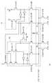
도 8은 도 7에 도시되어 있는 페이지 버퍼(PB)의 개략적인 구성을 보여주는 블록도이고, 도 9는 도 7에 도시되어 있는 페이지 버퍼(PB)의 상세 구성을 보여주는 회로도이다.8 is a block diagram illustrating a schematic configuration of the page buffer PB illustrated in FIG. 7, and FIG. 9 is a circuit diagram illustrating a detailed configuration of the page buffer PB illustrated in FIG. 7.
도 8 및 도 9를 참조하면, 본 발명에 따른 페이지 버퍼(PB)는 2개의 래치들, 즉 제 1 및 제 2 래치(51, 52)을 포함한다. 제 1 및 제 2 래치(51, 52)는 제 1 및 제 2 노드(N1, N2)를 통해 데이터 크로스 버스(data cross bus)에 선택적으로 연결된다. 데이터 크로스 버스에 연결되는 래치들(51, 52)의 개수는 제어 로직(190)의 제어에 의해 1개 또는 복수 개로 조절 가능하다. 데이터 크로스 버스는 페이지 버퍼 회로(150)와 비트 라인 선택 및 바이어스 회로(140) 사이에서, 페이지 버퍼 회로(150)와 비트라인 간의 데이터 인터페이스를 수행한다. 비트 라인 선택 및 바이어스 회로(140)는, 제어 로직(190)의 제어에 응답해서 제 1 메모리 셀(Cell-1)과 연결된 비트라인 쌍(BLe1, BLo1)과, 제 2 메모리 셀(Cell-2)과 연결된 비트라인 쌍(BLe2, BLo2)을 데이터 크로스 버스에 선택적으로 접속하는 역할을 수행한다. 한편, 제 1 래치(51)는 데이터 라인(DL)을 통해서 데이터 IO 버스(data IO bus)에 연결된다. 데이터 IO 버스는 페이지 버퍼 회로(150)와 외부(또는 호스트)와의 데이터 인터페이스를 수행한다.8 and 9, the page buffer PB according to the present invention includes two latches, namely, first and
도 10은 도 7 내지 도 9에 도시된 페이지 버퍼(PB)에 구비된 제 1 및 제 2 래치(51, 52)에 할당된 기능을 보여주는 도면이다.FIG. 10 is a diagram illustrating a function allocated to the first and
도 10을 참조하면, 메모리 셀에 저장되는 비트 수에 따라서 제 1 및 제 2 래치(51, 52)가 수행하는 기능이 각각 결정됨을 알 수 있다. 제 1 및 제 2 래치(51, 52)는 제어 로직(190)의 제어에 따라서, 제 1 및 제 2 메모리 셀(Cell-1, Cell-2)에 대응되는 비트라인 쌍((BLe1, BLo1), (BLe2, BLo2))에 각각 연결될 수 있고, 제 1 및 제 2 메모리 셀(Cell-1, Cell-2) 중 어느 하나에 대응되는 비트라인 쌍((BLe1, BLo1), 또는 (BLe2, BLo2))에 연결될 수 있다. 제 1 및 제 2 래치(51, 52)와 비트라인들의 연결 관계와, 제 1 및 제 2 래치(51, 52)에서 각각 수행되는 기능은, 메모리 셀에 저장되는 비트 수에 따라(즉, 퓨징 옵션이나 레지스터 셋팅 결과에 따라서) 제어 로직(190)에서 결정된다.Referring to FIG. 10, it can be seen that the functions performed by the first and
예를 들면, 하나의 메모리 셀에 1 비트(즉, 2 레벨)의 데이터가 저장되는 경우, 제 1 래치(51)는 제 1 및 제 2 메모리 셀(Cell-1, Cell-2) 중 어느 하나의 프로그램/독출 동작을 수행하는데 사용되고, 제 2 래치(52)는 다음에 프로그램될 데이터를 저장하는 캐쉬로서 사용된다. 제 1 래치(51)에 저장된 데이터는 대응되는 비트라인(제 1 및 제 2 메모리 셀(Cell-1, Cell-2) 중 어느 하나에 연결된 짝수번째 또는 홀수번째 비트라인)을 통해 프로그램되며, 상기 프로그램된 데이터는 제 1 래치(51)를 통해 독출된다. 그리고, 하나의 메모리 셀에 1.5 비트(즉, 3 레벨)의 데이터가 저장되는 경우(즉, 두 개의 메모리 셀에 3 비트의 데이터가 저장되는 경우), 제 1 래치(51)는 제 1 메모리 셀(Cell-1)에 대한 프로그램/독출 동작을 수행하고, 제 2 래치(52)는 제 2 메모리 셀(Cell-2)에 대한 프로그램/독출 동작을 각각 수행한다. 단위 메모리 셀에 1 비트의 데이터가 저장되는 메모리 셀과, 단위 메모리 셀에 1.5 비트가 저장되는 메모리 셀은 단일 비트 메모리 셀에 해당된다.For example, when one bit (ie, two levels) of data is stored in one memory cell, the
하나의 메모리 셀에 2 비트(즉, 4 레벨)의 데이터가 저장되는 경우, 하나의 메모리 셀에 2.5 비트(즉, 6 레벨), 또는 하나의 메모리 셀에 3 비트(즉, 8 레벨)의 데이터가 저장되는 경우의 각 래치의 역할을 살펴보면 다음과 같다. 제 1 래치(51)는 제 1 및 제 2 메모리 셀(Cell-1, Cell-2) 중 어느 하나의 프로그램/독출 동작을 수행하는데 사용되고, 제 2 래치(52)는 제 1 래치(51)에 의해 수행되는 프로그램 동작 바로 이전에 수행된 프로그램 데이터를 상기 메모리 셀(Cell-1 또는 Cell-2)로부터 읽어들이는 기능을 수행한다. 이 분야의 통상의 지식을 가진 이들에게 잘 알려져 있는 바와 같이, 멀티 비트 프로그램은 복수의 프로그램 단계들로 구성되며, 각각의 프로그램 단계에서는 이전 단계에서 수행된 프로그램 결과와 현재 단계에서 수행될 프로그램 데이터를 근거로 하여 프로그램 동작이 수행된다. 제 2 래치(52)를 이용하여 이전에 수행된 프로그램 결과가 읽혀지고 나면, 제 1 래치(51)에 로딩되어 있는 프로그램 데이터가 대응되는 메모리 셀로 프로그램된다. 단위 메모리 셀에 2 비트, 2.5 비트, 또는 3 비트의 데이터가 저장되는 메모리 셀은 멀티 비트 메모리 셀에 해당된다. 여기서, 단위 메모리 셀에 2 비트의 데이터가 저장되는 경우 제 1 및 제 2 래치(51, 52)에 할당되는 기능은, 2 비트 뿐만 아니라, 2n비트(예를 들면, 4 비트, 8 비트, 16 비트 등)의 다른 데이터 형태에도 적용 가능하다.When 2 bits (
아래에서는 본 발명의 페이지 버퍼 회로(150)를 이용한 프로그램 동작이 예시적으로 설명될 것이다. 본 발명의 페이지 버퍼 회로(150)에서는 메모리 셀에 저장되는 비트 수에 따라서 래치들의 기능이 각기 다르게 정의된다.Hereinafter, a program operation using the
도 11은 하나의 메모리 셀에 2.5 비트(즉, 6 레벨)의 데이터가 저장되는 경우(즉, 두 개의 메모리 셀에 5 비트의 데이터가 저장되는 경우)의 플래시 메모리 셀의 문턱 전압 분포를 보여주는 도면이다. 도 11에는 두 개의 메모리 셀들이 초기 값으로 가질 수 있는 1/1, 1/0, 0/1, 0/0의 데이터 상태 중 1/1의 데이터 상태에 대한 각 프로그램 단계별 문턱 전압 분포가 예시적으로 도시되어 있다. 도 10 및 도 11을 참조하여, 하나의 메모리 셀에 2.5 비트(즉, 6 레벨)의 데이터를 프로그램할 때의 본 발명에 따른 페이지 버퍼의 동작을 살펴보면 다음과 같다.FIG. 11 is a diagram illustrating a threshold voltage distribution of a flash memory cell when 2.5 bits (ie, 6 levels) of data are stored in one memory cell (that is, when 5 bits of data are stored in two memory cells). to be. FIG. 11 illustrates exemplary threshold voltage distributions for each program phase for a 1/1 data state among 1/1, 1/0, 0/1, and 0/0 data states that two memory cells may have as initial values. Is shown. Referring to FIGS. 10 and 11, the operation of the page buffer according to the present invention when programming 2.5 bits (ie, six levels) of data into one memory cell is as follows.
도 12는 6 레벨 MLC 프로그램의 4번째 프로그램에 대응되는 문턱 전압의 변화를 보여주는 도면이다. 그리고, 도 13은 6 레벨 MLC 프로그램의 4번째 프로그램 방법을 보여주는 흐름도이다. 도 12 및 도 13은 도 7 내지 도 9에 도시된 듀얼 래치 구조의 페이지 버퍼 회로(150)에서 수행되는 프로그램 동작을 예로 든 것이다. 6 레벨 MLC 프로그램은 하나의 메모리 셀에 2.5 비트가 저장되도록 하는 것으로서, 2개의 메모리 셀에 총 5비트의 데이터가 저장된다. 그러므로, 도 12 및 도 13에는 2 개의 메모리 셀(Cell-1, Cell-2)에 대한 문턱 전압의 변화와 프로그램 방법이 도시되어 있다.12 is a view showing a change in threshold voltage corresponding to the fourth program of the six-level MLC program. 13 is a flowchart illustrating a fourth program method of a six-level MLC program. 12 and 13 illustrate program operations performed by the
먼저 도 12를 참조하면, 6 레벨 MLC 프로그램의 4번째 프로그램은 총 4 단계의 프로그램 동작으로 구성된다. 첫 번째 단계에서는 "4"의 데이터 상태에 있던 제 1 메모리 셀(Cell-1)의 문턱전압이 "6"의 데이터 상태의 문턱전압으로 이동한다(화살표 ① 참조). 두 번째 단계에서는 "3"의 데이터 상태에 있던 제 1 메모리 셀(Cell-1)의 문턱전압이 "5"의 데이터 상태의 문턱전압으로 이동한다(화살표 ② 참조). 세 번째 단계에서는 "2"의 데이터 상태에 있던 제 2 메모리 셀(Cell-2)의 문턱전압이 "6"의 데이터 상태의 문턱전압으로 이동한다(화살표 ③ 참조). 네 번째 단계에서는 "1"의 데이터 상태에 있던 제 2 메모리 셀(Cell-2)의 문턱전압이 "5"의 데이터 상태의 문턱전압으로 이동한다(화살표 ④ 참조).First, referring to FIG. 12, the fourth program of the six-level MLC program includes a total of four program operations. In the first step, the threshold voltage of the first memory cell Cell-1 in the data state of "4" moves to the threshold voltage of the data state of "6" (see arrow ①). In the second step, the threshold voltage of the first memory cell Cell-1 in the data state of "3" moves to the threshold voltage of the data state of "5" (see arrow ②). In the third step, the threshold voltage of the second memory cell Cell-2 in the data state of "2" moves to the threshold voltage of the data state of "6" (see arrow ③). In the fourth step, the threshold voltage of the second memory cell Cell-2 in the data state of "1" moves to the threshold voltage of the data state of "5" (see arrow ④).
도 8 및 도 9에 도시된 바와 같이, 2개의 래치를 구비한 1개의 페이지 버퍼(PB)는 2 개의 메모리 셀(Cell-1, Cell-2)에 연결되어 있다. 상기 페이지 버퍼(PB)에 구비된 제 1 및 제 2 래치(52, 52)는 제 1 및 제 2 메모리 셀(Cell-1, Cell-2)에 대한 프로그램/독출 동작을 각각 수행한다. 본 발명에 따른 듀얼 래치 구조의 페이지 버퍼 회로(150)를 이용하여 도 12의 프로그램을 수행하는 경우, 총 4회의 프로그램 동작과 총 4회의 프로그램 검증 동작을 필요로 한다. 아래에서 상세히 설명되겠지만, 본 발명의 다른 실시예에 따른 페이지 버퍼 회로(도 14의 250 참조)의 경우에는 1개의 페이지 버퍼(PB')당 3개의 래치들이 구비되기 때문에, 제 1 및 제 2 메모리 셀(Cell-1, Cell-2)에 대한 상기 프로그램을 1회의 프로그램 동작과 4회의 프로그램 검증 동작으로 단축시킬 수 있게 된다.As shown in FIGS. 8 and 9, one page buffer PB having two latches is connected to two memory cells Cell-1 and Cell-2. The first and
도 13을 참조하면, 제 1 메모리 셀(Cell-1)에서는 도 12에 도시된 제 1 및 제 2 단계의 동작이 수행된다. 그리고 제 2 메모리 셀(Cell-2)에서는 도 12에 도시된 제 3 및 제 4 단계의 동작이 각각 수행된다. 제 1 메모리 셀(Cell-1)과 제 2 메모리 셀(Cell-2)에 대한 프로그램 동작은 2개의 래치(51, 52)가 구비된 1개의 페이지 버퍼(PB)를 통해 수행된다. 상기 페이지 버퍼(PB)의 구성은 도 8 및 도 9에 도시되어 있다.Referring to FIG. 13, the first and second steps of FIG. 12 are performed in the first memory cell Cell-1. In the second memory cell Cell-2, the operations of the third and fourth steps illustrated in FIG. 12 are performed, respectively. Program operations on the first memory cell Cell-1 and the second memory cell Cell-2 are performed through one page buffer PB provided with two
먼저, 제 1 메모리 셀(Cell-1)에 대한 4번째 프로그램의 제 1 단계 동작을 수행하기 위해, 제 1 래치(51)로 프로그램 데이터가 로딩된다(S1000 단계). 이어서, 제 2 래치(52)를 통해 제 1 메모리 셀(Cell-1)로부터 "4"의 데이터 상태가 읽 혀진다(S1100 단계). 그리고 나서, S1000 단계에서 로딩된 데이터 값과, S1100 단계에서 읽혀진 "4"의 데이터 상태에 대한 읽기 결과를 근거로 하여 "4"의 데이터 상태를 "6"의 데이터 상태로 프로그램하고, 프로그램 결과를 검증한다(S1200 단계). S1200 단계에서 수행되는 프로그램 및 검증 동작은, 제 1 메모리 셀(Cell-1)에서 "4"의 데이터 상태가 "6"의 데이터 상태로 정상적으로 프로그램될 때까지 제 1 래치(51)를 이용하여 반복 수행된다.First, in order to perform the first step operation of the fourth program for the first memory cell Cell-1, program data is loaded into the first latch 51 (step S1000). Subsequently, the data state of "4" is read from the first memory cell Cell-1 through the second latch 52 (step S1100). Then, the data state of "4" is programmed to the data state of "6" based on the data value loaded in step S1000 and the read result of the data state of "4" read in step S1100, and the program result is programmed. Verify (step S1200). The program and verify operation performed in step S1200 is repeated using the
이어서, 제 1 메모리 셀(Cell-1)에 대한 4번째 프로그램의 제 2 단계 동작을 수행하기 위해, "3"의 데이터 상태가 제 2 래치(52)를 통해 읽혀진다(S1300 단계). 그리고 나서, S1000 단계에서 로딩된 데이터 값과, S1300 단계에서 읽혀진 "3"의 데이터 상태에 대한 읽기 결과를 근거로 하여 "3"의 데이터 상태를 "5"의 데이터 상태로 프로그램하고, 프로그램 결과를 검증한다(S1400 단계). S1400 단계에서 수행되는 프로그램 및 검증 동작은, 제 1 메모리 셀(Cell-1)에서 "3"의 데이터 상태가 "5"의 데이터 상태로 정상적으로 프로그램될 때까지 제 1 래치(51)를 이용하여 반복 수행된다.Subsequently, in order to perform the second operation of the fourth program for the first memory cell Cell-1, the data state of "3" is read through the second latch 52 (step S1300). Then, the data state of "3" is programmed to the data state of "5" based on the data value loaded in step S1000 and the read result of the data state of "3" read in step S1300, and the program result is programmed. Verify (step S1400). The program and verify operation performed in step S1400 is repeated using the
계속해서, 제 2 메모리 셀(Cell-2)에 대한 4번째 프로그램의 제 3 단계 동작을 수행하기 위해 제 1 래치(51)로 프로그램 데이터가 로딩된다(S1500 단계). 제 1 메모리 셀(Cell-1)이 프로그램되는 동안 제 2 래치(52)의 값이 초기화 된다. 이어서, 제 2 래치(52)를 통해 제 2 메모리 셀(Cell-2)로부터 "2"의 데이터 상태가 읽혀진다(S1600 단계). 그리고 나서, S1500 단계에서 로딩된 데이터 값과, S1600 단계에서 읽혀진 "2"의 데이터 상태에 대한 읽기 결과를 근거로 하여 "2"의 데이터 상태를 "6"의 데이터 상태로 프로그램하고, 프로그램 결과를 검증한다(S1600 단계). S1600 단계에서 수행되는 프로그램 및 검증 동작은, 제 2 메모리 셀(Cell-2)에서 "2"의 데이터 상태가 "6"의 데이터 상태로 정상적으로 프로그램될 때까지 제 1 래치(51)를 이용하여 반복 수행된다.Subsequently, program data is loaded into the
이어서, 제 2 메모리 셀(Cell-2)에 대한 4번째 프로그램의 제 4 단계 동작을 수행하기 위해, 제 2 래치(52)가 리셋 된다(S1800 단계). 리셋 된 제 2 래치(52)는 프로그램 금지 상태가 된다. 그러므로, 제 1 래치(51)에 의해 "1"의 데이터 상태가 "5"의 데이터 상태로 프로그램되고, 상기 프로그램 결과가 검증된다(S1800 단계). S1800 단계에서 수행되는 프로그램 및 검증 동작은, 제 2 메모리 셀(Cell-2)에서 "1"의 데이터 상태가 "5"의 데이터 상태로 정상적으로 프로그램될 때까지 제 1 래치(51)를 이용하여 반복 수행된다.Subsequently, in order to perform the fourth step operation of the fourth program for the second memory cell Cell-2, the
이상과 같은 프로그램 동작을 수행하기 위한 각 래치(51, 52)의 역할은 제어 로직(190)의 제어에 의해 결정된다. 제어 로직(190)에 의해 결정되는 각 래치(51, 52)의 역할은 메모리 셀들에 저장되는 비트 수의 변환 결과(즉, 퓨징 옵션, 레지스터 세팅 등의 결과)에 따라 달라지게 된다. 각각의 메모리 셀에 저장되는 비트 수는 2의 멱지수 형태(즉, 2n 형태)가 될 수도 있고, 2의 멱지수 형태가 아닐 수도 있다(예를 들면, 2n-1 형태). 즉, 각각의 메모리 셀에 저장되는 비트 수에 따라서 낸드 스트링에 할당되는 메모리 셀들의 개수가 정의되고, 각각의 블록에 할당되는 페이지 개수가 정의된다. 이 경우, 낸드 스트링에 할당되는 메모리 셀의 개수는 2의 멱지수 형태가 아닐 수 있으나(예를 들면, 2n-1 형태), 각각의 블록에 할당되는 페이지 개수는 2의 멱지수 형태(즉, 2n 형태)가 된다. 따라서, 별도의 회로를 구비하지 않고도 기존의 메모리 장치들과 호환될 수 있게 된다.The role of each
한편, 본 발명에 따른 플래시 메모리 장치(100)는, 각각의 메모리 블록마다 서로 다른 페이지 개수가 할당될 수 있다. 각각의 메모리 블록에 할당되는 페이지의 개수는 각각의 메모리 셀에 할당되는 비트 수에 대한 정보를 나타내는 퓨징 옵션 또는 레지스터 세팅 결과를 근거로 산출된다. 이 경우, 본 발명에 따른 플래시 메모리 장치(100)는 각각의 메모리 블록에 할당된 페이지 개수에 적합한 프로그램 및 독출 동작을 수행하기 위해, 각각의 페이지 버퍼에 구비된 래치들의 기능을 개별적으로 제어할 수 있다. 따라서, 동일한 페이지 버퍼의 회로 구성을 가지고도 다양한 형태의 메모리 셀들에 대한 프로그램 및 독출 동작을 수행할 수 있게 된다.Meanwhile, in the
도 14는 본 발명의 다른 실시예에 따른 플래시 메모리 장치(200)의 구성을 보여주는 블록도로서, 트리플 래치 구조(triple latch structure)의 페이지 버퍼 회로(250)를 구비한 멀티-비트 플래시 메모리 장치(200)의 구조가 도시되어 있다.FIG. 14 is a block diagram illustrating a configuration of a
도 14를 참조하면, 본 발명에 따른 플래시 메모리 장치(200)는 페이지 버퍼 회로(250)의 구성을 제외하면 도 7에 도시된 플래시 메모리 장치(100)와 사실상 동일한 구성을 갖는다. 따라서, 동일한 구성 요소에 대해서는 동일한 참조 번호를 부가하고, 이들에 대한 중복되는 설명은 생략하기로 한다.Referring to FIG. 14, the
도 15는 도 14에 도시되어 있는 페이지 버퍼(PB')의 개략적인 구성을 보여주 는 블록도이고, 도 16는 도 14에 도시되어 있는 페이지 버퍼(PB')의 상세 구성을 보여주는 회로도이다.FIG. 15 is a block diagram illustrating a schematic configuration of the page buffer PB 'illustrated in FIG. 14, and FIG. 16 is a circuit diagram illustrating a detailed configuration of the page buffer PB ′ illustrated in FIG. 14.
도 14 내지 도 16을 참조하면, 본 발명에 따른 페이지 버퍼(PB')는 3개의 래치들(51-53)을 포함한다. 각각의 래치(51-53)가 수행하는 기능은, 메모리 셀에 저장될 데이터 비트 수를 근거로 하여 제어 로직(190)에서 결정된다. 결정된 데이터 비트 수에 관한 정보는 제어 로직(190)에 세팅된다. 제어 로직(190)은 상기 세팅된 정보를 이용하여 각각의 래치(51-53)가 수행하는 기능을 결정한다. 상기 래치(51-53)의 기능은 하나 또는 그 이상의 메모리 블록 단위로 정의될 수 있다.14 to 16, the page buffer PB ′ according to the present invention includes three latches 51-53. The function that each latch 51-53 performs is determined by the
제 1 내지 제 3 래치(51-53)는 제 1 및 제 2 노드(N1, N2)를 통해 데이터 크로스 버스(data cross bus)에 선택적으로 연결된다. 데이터 크로스 버스에 연결되는 래치들의 개수는 제어 로직(190)의 제어에 의해 1개 또는 복수 개로 조절 가능하다. 데이터 크로스 버스는 페이지 버퍼 회로(250)와 비트 라인 선택 및 바이어스 회로(140) 사이에서, 페이지 버퍼 회로(250)와 비트라인 간의 데이터 인터페이스를 수행한다. 비트 라인 선택 및 바이어스 회로(140)는, 제어 로직(190)의 제어에 응답해서 제 1 메모리 셀(Cell-1)과 연결된 비트라인 쌍(BLe1, BLo1)과, 제 2 메모리 셀(Cell-2)과 연결된 비트라인 쌍(BLe2, BLo2)을 데이터 크로스 버스에 선택적으로 접속하는 역할을 수행한다. 한편, 제 1 및 제 3 래치(51, 53)는 데이터 라인(DL)을 통해서 데이터 IO 버스(data IO bus)에 연결된다. 데이터 IO 버스는 페이지 버퍼 회로(250)와 외부(또는 호스트)와의 데이터 인터페이스를 수행한다. 데이터 IO 버스에 연결된 제 1 및 제 3 래치(51, 53)의 데이터 입출력 동작은 각각 독립적으로 수행된다. 이와 같은 구성에 따르면, 멀티 비트 프로그램 동작시 캐쉬 프로그램 동작을 지원할 수 있게 된다.The first to
도 17은 도 14 내지 도 16에 도시된 페이지 버퍼(PB')에 구비된 제 1 내지 제 3 래치(51-53)에 할당된 기능을 보여주는 도면이다.17 is a diagram illustrating a function allocated to the first to
도 17을 참조하면, 메모리 셀에 저장되는 비트 수에 따라서 제 1 내지 제 3 래치(51-53)가 수행하는 기능이 각각 결정됨을 알 수 있다. 제 1 내지 제 3 래치(51-53)는 제어 로직(190)의 제어에 따라서, 제 1 및 제 2 메모리 셀(Cell-1, Cell-2)에 대응되는 비트라인 쌍((BLe1, BLo1), (BLe2, BLo2))에 각각 연결될 수 있고, 제 1 및 제 2 메모리 셀(Cell-1, Cell-2) 중 어느 하나에 대응되는 비트라인 쌍((BLe1, BLo1), 또는 (BLe2, BLo2))에 연결될 수 있다. 제 1 내지 제 3 래치(51-53)와 비트라인들의 연결 관계와, 제 1 내지 제 3 래치(51-53)에서 각각 수행되는 기능은, 메모리 셀에 저장되는 비트 수에 따라(즉, 퓨징 옵션이나 레지스터 셋팅 결과에 따라서) 제어 로직(190)에서 결정된다.Referring to FIG. 17, it can be seen that the functions performed by the first to
예를 들면, 하나의 메모리 셀에 1 비트(즉, 2 레벨)의 데이터가 저장되는 경우, 제 1 래치(51)는 제 1 및 제 2 메모리 셀(Cell-1, Cell-2) 중 어느 하나의 프로그램/독출 동작을 수행하는데 사용되고, 제 2 래치(52)는 다음에 프로그램될 데이터를 저장하는 캐쉬로서 사용된다. 제 1 래치(51)에 저장된 데이터는 대응되는 비트라인(제 1 및 제 2 메모리 셀(Cell-1, Cell-2) 중 어느 하나에 연결된 짝수번째 또는 홀수번째 비트라인)을 통해 프로그램되며, 상기 프로그램된 데이터는 제 1 래치(51)를 통해 독출된다. 그리고, 하나의 메모리 셀에 1.5 비트(즉, 3 레벨)의 데이터가 저장되는 경우(즉, 두 개의 메모리 셀에 3 비트의 데이터가 저장되는 경우), 제 1 래치(51)는 제 1 메모리 셀(Cell-1)에 대한 프로그램/독출 동작을 수행하고, 제 2 래치(52)는 제 2 메모리 셀(Cell-2)에 대한 프로그램/독출 동작을 각각 수행한다. 그리고, 제 3 래치(53)는 다음에 프로그램될 데이터를 저장하는 캐쉬로서 사용된다. 단위 메모리 셀에 1 비트의 데이터가 저장되는 메모리 셀과, 단위 메모리 셀에 1.5 비트가 저장되는 메모리 셀은 단일 비트 메모리 셀에 해당된다.For example, when one bit (ie, two levels) of data is stored in one memory cell, the
하나의 메모리 셀에 2 비트(즉, 4 레벨)의 데이터가 저장되는 경우, 또는 하나의 메모리 셀에 3 비트(즉, 8 레벨)의 데이터가 저장되는 경우의 각 래치의 역할을 살펴보면 다음과 같다. 제 1 래치(51)는 제 1 및 제 2 메모리 셀(Cell-1, Cell-2) 중 어느 하나의 프로그램/독출 동작을 수행하는데 사용되고, 제 2 래치(52)는 제 1 래치(51)에 의해 수행되는 프로그램 동작 바로 이전에 수행된 프로그램 데이터를 상기 메모리 셀(Cell-1 또는 Cell-2)로부터 읽어들이는 기능을 수행한다. 그리고, 제 3 래치(53)는 다음에 프로그램될 데이터를 저장하는 캐쉬로서의 기능을 수행한다. 이 분야의 통상의 지식을 가진 이들에게 잘 알려져 있는 바와 같이, 멀티 비트 프로그램은 복수의 프로그램 단계들로 구성되며, 각각의 프로그램 단계에서는 이전 단계에서 수행된 프로그램 결과와 현재 단계에서 수행될 프로그램 데이터를 근거로 하여 프로그램 동작이 수행된다. 제 2 래치(52)를 이용하여 이전에 수행된 프로그램 결과가 읽혀지고 나면, 제 1 래치(51)에 로딩되어 있는 프로그램 데이터가 대응되는 메모리 셀로 프로그램된다. 단위 메모리 셀에 복수 개의 비트(예를 들면, 2 비트, 2.5 비트, 3 비트 등)가 저장되는 메모리 셀은 멀티 비트 메모리 셀에 해당된다. 여기서, 단위 메모리 셀에 2 비트의 데이터가 저장되는 경우 제 1 및 제 2 래치(51, 52)에 할당되는 기능은, 2 비트 뿐만 아니라, 2n비트(예를 들면, 4 비트, 8 비트, 16 비트 등)의 다른 데이터 형태에도 적용 가능하다.The role of each latch when two bits (ie, four levels) of data are stored in one memory cell or three bits (ie, eight levels) of data in one memory cell is as follows. . The
한편, 하나의 메모리 셀에 2.5 비트(즉, 6 레벨)의 데이터가 저장되는 경우(즉, 두 개의 메모리 셀에 5 비트의 데이터가 저장되는 경우) 각 래치에 할당된 기능은 다음과 같다. 먼저 제 1 및 제 2 래치(51, 52)는 제 1 및 제 2 메모리 셀(Cell-1, Cell-2)에 프로그램될 데이터를 저장하는 기능을 각각 수행한다. 이때, 제 3 래치(53)는 이전에 프로그램된 1 또는 2 페이지의 데이터를 읽어들이는 기능을 수행한다. 제 3 래치(53)를 이용하여 읽어들인 이전의 프로그램 결과와, 제 1 및 제 2 래치(51, 52)에 저장된 데이터를 근거로 하여, 제 1 및 제 2 래치(51, 52)에 저장된 데이터에 대한 프로그램이 수행된다. 제 1 및 제 2 메모리 셀(Cell-1, Cell-2)에 대한 프로그램 동작은, 제 1 및 제 2 래치(51, 52)를 통해 각각 동시에 수행되며, 상기 프로그램된 데이터는 제 1 및 제 2 래치(51, 52)를 통해 각각 독출된다. 제 3 래치(53)에 저장된 데이터는 제 1 및 제 2 래치들(51, 52)에 저장되어 있는 데이터를 구분하는데 사용된다. 본 발명에 따른 트리플 래치 구조의 페이지 버퍼 회로(250)에서 수행되는 6 레벨 MLC 프로그램 동작은 도 18 및 도 19를 참조하여 설명될 것이다.Meanwhile, when 2.5 bits (ie, 6 levels) of data are stored in one memory cell (that is, when 5 bits of data are stored in two memory cells), the functions assigned to each latch are as follows. First, the first and
도 18은 6 레벨 MLC 프로그램의 4번째 프로그램에 대응되는 문턱 전압의 변화를 보여주는 도면이다. 그리고, 도 19는 6 레벨 MLC 프로그램의 4번째 프로그램 방법을 보여주는 흐름도이다. 도 18 및 도 19는 도 14 내지 도 16에 도시된 트리플 래치 구조의 페이지 버퍼 회로(250)에서 수행되는 프로그램 동작을 예로 든 것이다. 6 레벨 MLC 프로그램은 하나의 메모리 셀에 2.5 비트가 저장되도록 하는 것으로서, 2개의 메모리 셀에 총 5비트의 데이터가 저장된다. 그러므로, 도 18 및 도 19에는 2 개의 메모리 셀(Cell-1, Cell-2)에 대한 문턱 전압의 변화와 프로그램 방법이 도시되어 있다.18 is a diagram illustrating a change in threshold voltage corresponding to the fourth program of the six-level MLC program. 19 is a flowchart illustrating a fourth program method of a six-level MLC program. 18 and 19 illustrate a program operation performed in the
먼저 도 18을 참조하면, 6 레벨 MLC 프로그램의 4번째 프로그램은 도 12에서 설명한 바와 마찬가지로 총 4 단계의 프로그램 동작으로 구성된다. 상기 4 단계의 프로그램 동작은, 트리플 래치 구조의 페이지 버퍼 회로(250)를 이용하여 제 1 및 제 2 메모리 셀(Cell-1, Cell-2) 각각에서 동시에 수행된다(화살표 ①, ①', ②, ②' 참조). 반면에, 동시에 수행된 4 단계의 프로그램 동작에 대한 검증은 각각 개별적으로 수행된다. 즉, 트리플 래치 구조의 페이지 버퍼 회로(250)를 이용한 6 레벨 MLC 프로그램의 4번째 프로그램 동작은, 총 1회의 프로그램 동작과 4회의 프로그램 검증 동작으로 구성된다. 여기서, 프로그램 검증 동작은 인접 메모리 셀들의 독출시 비트라인으로 인가되는 전압의 특성상 동시에 수행되지는 못하고 개별적으로 수행된다. 트리플 래치 구조의 페이지 버퍼 회로(250)를 이용한 구체적인 프로그램 동작은 다음과 같다.First, referring to FIG. 18, the fourth program of the six-level MLC program includes a total of four program operations as described with reference to FIG. 12. The four-step program operation is simultaneously performed in each of the first and second memory cells Cell-1 and Cell-2 using the triple buffer structure page buffer circuit 250 (
도 19를 참조하면, 먼저 4번째 프로그램의 제 1 단계 동작을 수행하기에 앞서 제 1 내지 제 3 래치들(51-53)이 리셋(또는 초기화) 된다(S2000 단계). 제 1 래치(51)와 제 2 래치(52)로 프로그램 데이터가 각각 로딩된다(S2100 단계). 이어서, 제 3 래치(53)를 통해 제 1 메모리 셀(Cell-1)에 프로그램되어 있는 데이터가 읽혀진다(S2200 단계). 그리고, S2200 단계에서 읽혀진 데이터를 근거로 하여 제 1 메모리 셀(Cell-1)에 프로그램되어 있는 데이터의 문턱전압이 '2'의 데이터 상태보다 높은 값을 갖는지 여부가 판별된다(S2300 단계).Referring to FIG. 19, first of all, the first to
S2300 단계에서의 판별 결과, 제 1 메모리 셀(Cell-1)에 프로그램되어 있는 데이터가 '2'의 데이터 상태보다 높은 값을 가지면, 제 2 래치(52)는 데이터 '1'의 상태로 초기화된다(S2400 단계). 제 1 메모리 셀(Cell-1)에 프로그램되어 있는 데이터가 '2'의 데이터 상태보다 높은 값을 가진다는 것은, 제 1 메모리 셀(Cell-1)에 '3' 또는 '4'의 데이터가 저장되어 있다는 것을 알 수 있다. 이 경우, 제 1 래치(51)는 제 1 메모리 셀(Cell-1)의 프로그램에 사용되도록 설정된다. 그리고, 초기화된 제 2 래치(52)는 제 2 메모리 셀(Cell-2)의 프로그램에 사용되도록 설정된다.As a result of the determination in operation S2300, when the data programmed in the first memory cell Cell-1 has a higher value than the data state of '2', the
반면에, S2300 단계에서의 판별 결과, 제 1 메모리 셀(Cell-1)에 프로그램되어 있는 데이터가 '2'의 데이터 상태보다 낮은 데이터 상태를 가지면, 제 1 래치(51)는 초기화된다(S2450 단계). 제 1 메모리 셀(Cell-1)에 프로그램되어 있는 데이터가 '2'의 데이터 상태보다 낮은 값을 가진다는 것은, 제 1 메모리 셀(Cell-1)에 '1' 또는 '2'의 데이터가 저장되어 있다는 것을 알 수 있다. 이 경우, 제 2 메모리 셀(Cell-1)에는 '3' 또는 '4'의 데이터가 저장되어 있을 것이다. 따라서, 초기화된 제 1 래치(51)는 제 1 메모리 셀(Cell-1)의 프로그램에 사용되도록 설정된다. 그리고, 제 2 래치(52)는 제 2 메모리 셀(Cell-1)의 프로그램에 사용되도록 설정된다. 앞에서 설명한 바와 같이, S2200 단계에서 읽어들인 제 1 메모리 셀(Cell-1)의 프로그램 상태는, 제 1 및 제 2 래치(51, 52)의 기능을 설정하는데 사용된다.On the other hand, when the determination result in step S2300, if the data programmed in the first memory cell (Cell-1) has a data state lower than the data state of '2', the
이어서, 제 3 래치(53)를 이용하여 제 1 메모리 셀(Cell-1)에 프로그램되어 있는 데이터를 읽어들인다(S2500 단계). S2500 단계에서 읽어들인 데이터는 제 1 메모리 셀(Cell-1)에 저장되어 있는 데이터가 '3'의 데이터 상태에 있는지 또는 '4'의 데이터 상태에 있는지(또는, '1'의 데이터 상태에 있는지 또는 '2'의 데이터 상태에 있는지) 여부를 결정한다. 그리고 나서, 제 3 래치(53)를 이용하여 제 2 메모리 셀(Cell-2)에 프로그램되어 있는 데이터를 읽어들인다(S2600 단계). S2600 단계에서 읽어들인 데이터는 제 2 메모리 셀(Cell-2)에 저장되어 있는 데이터가 '1'의 데이터 상태에 있는지 또는 '2'의 데이터 상태에 있는지(또는, '3'의 데이터 상태에 있는지 또는 '4'의 데이터 상태에 있는지) 여부를 결정한다.Subsequently, data programmed in the first memory cell Cell-1 is read using the third latch 53 (step S2500). The data read in step S2500 is whether the data stored in the first memory cell Cell-1 is in the data state of '3' or in the data state of '4' (or in the data state of '1'). Or '2' data state). Then, the data programmed in the second memory cell Cell-2 is read using the third latch 53 (step S2600). The data read in step S2600 is whether the data stored in the second memory cell (Cell-2) is in the data state of '1' or in the data state of '2' (or in the data state of '3'). Or '4' data state).
계속해서, S2500 단계 및 S2600 단계에서 읽어들인 데이터와 제 1 및 제 2 래치(51, 52)로 로딩된 프로그램 데이터를 근거로 하여, 도 18에 도시되어 있는 총 4 단계의 프로그램 동작(화살표 ①, ①', ②, ②' 참조)이 제 1 및 제 2 메모리 셀(Cell-1, Cell-2)에서 동시에 수행된다(S2700 단계). S2700 단계에서 수행되는 프로그램 동작은, 화살표 ①과 화살표 ②로 표시된 프로그램 동작이 수행된 후에, 증가된 프로그램 전압을 이용하여 화살표 ①'과 화살표 ②'로 표시된 프로그램 동작이 연속해서 수행된다. 예를 들면, S2700 단계에서는 제 1 메모리 셀(Cell-1)에서 '3'의 데이터 상태(또는 '1'의 데이터 상태)가 '5'의 데이터 상태로 프로그램된 후, 단계적으로 증가된 프로그램 전압을 이용하여 '4'의 데이터 상태(또는 '2'의 데이터 상태)를 '6'의 데이터 상태로 프로그램한다. 이와 동시에, 제 2 메모리 셀(Cell-2)에서는 '1'의 데이터 상태(또는 '3'의 데이터 상태)가 '5'의 데이터 상태로 프로그램된 후, 단계적으로 증가된 프로그램 전압을 이용하여 '2'의 데이터 상태(또는 '4'의 데이터 상태)를 '6'의 데이터 상태로 프로그램한다. S2700 단계의 프로그램 동작이 수행되고 나면, 제 1 및 제 2 메모리 셀(Cell-1, Cell-2)에서 상기 프로그램 동작이 올바로 수행되었는지 여부가 검증된다(S2800 단계).Subsequently, on the basis of the data read in the steps S2500 and S2600 and the program data loaded into the first and
S2800 단계에서 수행되는 프로그램 검증 동작은, 도 18에 도시된 화살표 ①, ①', ②, ②' 에 대응되는 총 4 단계의 프로그램 검증 동작으로 구성된 된다. 예를 들면, 제 1 메모리 셀(Cell-1)에서 '5'의 데이터 상태로 프로그램이 올바로 수행되었는지 여부가 판별된 후(즉, 화살표 ①에 대응되는 검증동작), 제 2 메모리 셀(Cell-2)에서 '5'의 데이터 상태로 프로그램이 올바로 수행되었는지 여부가 판별된다(즉, 화살표 ②에 대응되는 검증동작). 그리고 나서, 제 1 메모리 셀(Cell-1)에서 '6'의 데이터 상태로 프로그램이 올바로 수행되었는지 여부가 판별된 후(즉, 화살표 ①'에 대응되는 검증동작), 제 2 메모리 셀(Cell-2)에서 '6'의 데이터 상태로 프로그램이 올바로 수행되었는지 여부가 판별된다(즉, 화살표 ②'에 대응되는 검증 동작).The program verifying operation performed in step S2800 includes a total of 4 program verifying operations corresponding to the
S2800 단계에서 총 4 단계의 프로그램 검증 동작이 순차적으로 수행되고 나면, 메모리 셀들이 모두 프로그램되었는지 여부가 판별된다(S2900 단계). S2900 단계에서의 판별 결과, 메모리 셀들이 모두 프로그램되었으면 수순은 종료된다. 그리 고, 메모리 셀들이 모두 프로그램되지 않았으면 수순은 S2700 단계로 되돌아가서 프로그램 및 프로그램 검증 동작을 반복 수행한다.After a total of four program verification operations are sequentially performed in step S2800, it is determined whether all of the memory cells are programmed (step S2900). As a result of the determination in step S2900, if the memory cells are all programmed, the procedure ends. If the memory cells are not all programmed, the procedure returns to step S2700 to repeat the program and program verification operations.
앞에서 설명한 바와 같이, 본 발명에 따른 플래시 메모리 장치(200)는 메모리 셀에 저장되는 비트 수의 변환 결과(즉, 퓨징 옵션, 레지스터 세팅 등의 결과)에 따라서 페이지 버퍼에 구비된 래치들의 역할을 제어한다. 각 래치들의 역할은 각각의 메모리 블록마다(또는 복수 개의 메모리 블록마다) 서로 다르게 정의되고 제어될 수 있다. 특히, 각각의 래치들은 제어 로직(190)의 제어에 따라서 데이터 크로스 버스에 선택적으로 연결될 수 있으며, 각각의 래치들에 대한 데이터 입출력이 각각 독립적으로 수행될 수 있다. 따라서, 복수 개의 래치들에 대한 동시 동작이 가능해 지고, 멀티 비트 프로그램 동작시 캐쉬 프로그램 기능을 지원할 수 있게 된다. 그 결과, 동일한 페이지 버퍼의 회로 구성을 가지고도 다양한 형태의 메모리 셀들, 예를 들면 다양한 종류의 멀티 비트 셀에 유동적으로 적용될 수 있다. 따라서, 칩 사이즈가 줄어들게 된다.As described above, the
이상에서와 같이 도면과 명세서에서 최적 실시예가 개시되었다. 여기서 특정한 용어들이 사용되었으나, 이는 단지 본 발명을 설명하기 위한 목적에서 사용된 것이지 의미 한정이나 특허청구범위에 기재된 본 발명의 범위를 제한하기 위하여 사용된 것은 아니다. 그러므로 본 기술 분야의 통상의 지식을 가진 자라면 이로부터 다양한 변형 및 균등한 타 실시예가 가능하다는 점을 이해할 것이다. 따라서, 본 발명의 진정한 기술적 보호 범위는 첨부된 특허청구범위의 기술적 사상에 의해 정해져야 할 것이다.As described above, optimal embodiments have been disclosed in the drawings and the specification. Although specific terms have been used herein, they are used only for the purpose of describing the present invention and are not used to limit the scope of the present invention as defined in the meaning or claims. Therefore, those skilled in the art will understand that various modifications and equivalent other embodiments are possible from this. Therefore, the true technical protection scope of the present invention will be defined by the technical spirit of the appended claims.
이상과 같은 본 발명에 의하면, 플래시 메모리 장치의 주변 회로, 파일 시스템의 제어 방식, 또는 블록 사이즈 등을 변경하지 않고도 기존의 플래시 메모리 장치들간의 호환성을 보장할 수 있으며, 다양한 종류의 멀티 비트 셀에 대한 프로그램, 소거 및 독출 동작을 수행할 수 있다.According to the present invention as described above, it is possible to ensure compatibility between existing flash memory devices without changing the peripheral circuit of the flash memory device, the control method of the file system, the block size, etc. Program, erase, and read operations may be performed.
그리고, 본 발명에 따른 페이지 버퍼 및 플래시 메모리 장치는 메모리 셀에 저장되는 비트 수가 달라지더라도 달라진 비트 수에 대응되는 프로그램, 소거 및 기입 동작을 유동적으로 수행할 수 있어, 칩 사이즈를 효과적으로 줄일 수 있다.In addition, even if the number of bits stored in a memory cell is changed, the page buffer and the flash memory device according to the present invention can flexibly perform program, erase and write operations corresponding to the changed number of bits, thereby effectively reducing the chip size. .
Claims (30)
Translated fromKoreanPriority Applications (3)
| Application Number | Priority Date | Filing Date | Title |
|---|---|---|---|
| KR1020060104611AKR100773400B1 (en) | 2006-10-26 | 2006-10-26 | Multi-bit flash memory device |
| US11/657,642US7508732B2 (en) | 2006-10-26 | 2007-01-25 | Multi-bit flash memory device including memory cells storing different numbers of bits |
| CN2007103057694ACN101202105B (en) | 2006-10-26 | 2007-10-26 | Multi-bit flash memory device including memory cells storing different numbers of bits |
Applications Claiming Priority (1)
| Application Number | Priority Date | Filing Date | Title |
|---|---|---|---|
| KR1020060104611AKR100773400B1 (en) | 2006-10-26 | 2006-10-26 | Multi-bit flash memory device |
Publications (1)
| Publication Number | Publication Date |
|---|---|
| KR100773400B1true KR100773400B1 (en) | 2007-11-05 |
Family
ID=39060850
Family Applications (1)
| Application Number | Title | Priority Date | Filing Date |
|---|---|---|---|
| KR1020060104611AActiveKR100773400B1 (en) | 2006-10-26 | 2006-10-26 | Multi-bit flash memory device |
Country Status (3)
| Country | Link |
|---|---|
| US (1) | US7508732B2 (en) |
| KR (1) | KR100773400B1 (en) |
| CN (1) | CN101202105B (en) |
Cited By (8)
| Publication number | Priority date | Publication date | Assignee | Title |
|---|---|---|---|---|
| KR100876249B1 (en) | 2006-09-08 | 2008-12-26 | 가부시끼가이샤 도시바 | Nonvolatile semiconductor memory |
| WO2009111981A1 (en)* | 2008-03-11 | 2009-09-17 | 深圳市朗科科技股份有限公司 | Method for improving data access speed of flash media and apparatus employing this method |
| KR100967004B1 (en)* | 2008-08-05 | 2010-06-30 | 주식회사 하이닉스반도체 | How to control the operation of flash memory devices |
| US8339846B2 (en) | 2009-08-14 | 2012-12-25 | Samsung Electronics Co., Ltd. | Flash memory device, programming and reading methods performed in the same |
| WO2014003755A1 (en)* | 2012-06-28 | 2014-01-03 | Hewlett-Packard Development Company, L.P. | Multi-level cell memory |
| KR20190134096A (en)* | 2018-05-24 | 2019-12-04 | 에스케이하이닉스 주식회사 | Semiconductor memory device and operating method thereof |
| CN112310106A (en)* | 2019-08-01 | 2021-02-02 | 爱思开海力士有限公司 | Semiconductor memory device including page buffer |
| KR20220010260A (en)* | 2020-07-17 | 2022-01-25 | 에스케이하이닉스 주식회사 | Semiconductor memory device |
Families Citing this family (32)
| Publication number | Priority date | Publication date | Assignee | Title |
|---|---|---|---|---|
| KR100634457B1 (en)* | 2005-07-04 | 2006-10-16 | 삼성전자주식회사 | Flash memory device that performs multi-bit and single-bit program operations with a single page buffer structure |
| JP5072301B2 (en)* | 2006-09-25 | 2012-11-14 | 株式会社東芝 | Semiconductor integrated circuit device and operation method thereof |
| US7646636B2 (en)* | 2007-02-16 | 2010-01-12 | Mosaid Technologies Incorporated | Non-volatile memory with dynamic multi-mode operation |
| US7630252B2 (en)* | 2007-06-25 | 2009-12-08 | Sandisk Corporation | Systems for programming multilevel cell nonvolatile memory |
| US7719889B2 (en)* | 2007-06-25 | 2010-05-18 | Sandisk Corporation | Methods of programming multilevel cell nonvolatile memory |
| KR20090017270A (en)* | 2007-08-14 | 2009-02-18 | 삼성전자주식회사 | Multi-bit programming device and method |
| JP2009104729A (en)* | 2007-10-24 | 2009-05-14 | Toshiba Corp | Nonvolatile semiconductor memory device |
| EP2347417B1 (en)* | 2008-09-03 | 2018-04-18 | Marvell World Trade Ltd. | Programming data into a multi-plane flash memory |
| KR101074564B1 (en)* | 2009-02-04 | 2011-10-17 | 주식회사 하이닉스반도체 | Non volatile memory device |
| KR101066686B1 (en)* | 2009-06-29 | 2011-09-21 | 주식회사 하이닉스반도체 | Semiconductor memory device and reading method thereof |
| US8386884B2 (en)* | 2009-07-14 | 2013-02-26 | Macronix International Co., Ltd. | Memory apparatus with multi-level cells and operation method thereof |
| EP2473999A1 (en)* | 2009-08-31 | 2012-07-11 | SanDisk IL Ltd. | Preloading data into a flash storage device |
| KR101126514B1 (en)* | 2009-12-31 | 2012-03-29 | 주식회사 하이닉스반도체 | Semiconductor memory device and read method thereof |
| US8645794B1 (en)* | 2010-07-31 | 2014-02-04 | Apple Inc. | Data storage in analog memory cells using a non-integer number of bits per cell |
| KR20120070445A (en)* | 2010-12-21 | 2012-06-29 | 에스케이하이닉스 주식회사 | Page buffer circuit |
| US8482955B2 (en)* | 2011-02-25 | 2013-07-09 | Micron Technology, Inc. | Resistive memory sensing methods and devices |
| US9588883B2 (en)* | 2011-09-23 | 2017-03-07 | Conversant Intellectual Property Management Inc. | Flash memory system |
| US8902650B2 (en)* | 2012-08-30 | 2014-12-02 | Micron Technology, Inc. | Memory devices and operating methods for a memory device |
| KR102163872B1 (en) | 2013-08-09 | 2020-10-13 | 삼성전자 주식회사 | Multi-bit memory device, onchip buffered program method thereof and multi-bit memory system |
| US9412441B2 (en)* | 2013-08-13 | 2016-08-09 | SK Hynix Inc. | Semiconductor memory device |
| JP2015204126A (en)* | 2014-04-16 | 2015-11-16 | 株式会社東芝 | Semiconductor storage device |
| KR20170006977A (en)* | 2015-07-10 | 2017-01-18 | 에스케이하이닉스 주식회사 | Semiconductor memory device and operating method thereof |
| US10096355B2 (en) | 2015-09-01 | 2018-10-09 | Sandisk Technologies Llc | Dynamic management of programming states to improve endurance |
| KR102261816B1 (en) | 2017-12-05 | 2021-06-07 | 삼성전자주식회사 | Non-volatile memory device improving data reliability and Operating method thereof |
| US11150844B2 (en) | 2019-02-21 | 2021-10-19 | Micron Technology, Inc. | Reflow endurance improvements in triple-level cell NAND flash |
| CN111863074B (en) | 2019-04-28 | 2024-03-01 | 桑迪士克科技有限责任公司 | Memory device having different bits per cell on different word lines in a block |
| US11243711B2 (en) | 2020-02-05 | 2022-02-08 | Micron Technology, Inc. | Controlling firmware storage density based on temperature detection |
| US11144452B2 (en) | 2020-02-05 | 2021-10-12 | Micron Technology, Inc. | Temperature-based data storage processing |
| US11587919B2 (en) | 2020-07-17 | 2023-02-21 | Micron Technology, Inc. | Microelectronic devices, related electronic systems, and methods of forming microelectronic devices |
| CN113409840A (en)* | 2021-06-30 | 2021-09-17 | 芯天下技术股份有限公司 | State register and write operation method, chip and device thereof |
| US11615839B2 (en) | 2021-07-06 | 2023-03-28 | Sandisk Technologies Llc | Non-volatile memory with variable bits per memory cell |
| KR20230057763A (en) | 2021-10-22 | 2023-05-02 | 삼성전자주식회사 | Page buffer including a plurality of latches and Memory device having the same |
Citations (1)
| Publication number | Priority date | Publication date | Assignee | Title |
|---|---|---|---|---|
| US6987693B2 (en) | 2002-09-24 | 2006-01-17 | Sandisk Corporation | Non-volatile memory and method with reduced neighboring field errors |
Family Cites Families (7)
| Publication number | Priority date | Publication date | Assignee | Title |
|---|---|---|---|---|
| JP3397600B2 (en) | 1996-11-01 | 2003-04-14 | 株式会社東芝 | Nonvolatile semiconductor memory device |
| KR100463195B1 (en)* | 2001-08-28 | 2004-12-23 | 삼성전자주식회사 | Non-volatile semiconductor memory device with accelerated column scanning scheme |
| KR100447969B1 (en) | 2001-09-13 | 2004-09-10 | 주식회사 하이닉스반도체 | Flash memory apparatus for multilevel and singlelevel program/read |
| JP2005092923A (en) | 2003-09-12 | 2005-04-07 | Renesas Technology Corp | Semiconductor memory device |
| KR100632946B1 (en)* | 2004-07-13 | 2006-10-12 | 삼성전자주식회사 | Nonvolatile Memory Device And Its Program Method |
| KR100723772B1 (en)* | 2005-03-28 | 2007-05-30 | 주식회사 하이닉스반도체 | Page Buffer of Flash Memory Device with Improved Program Operation Performance and Its Program Operation Control Method |
| KR100634457B1 (en)* | 2005-07-04 | 2006-10-16 | 삼성전자주식회사 | Flash memory device that performs multi-bit and single-bit program operations with a single page buffer structure |
- 2006
- 2006-10-26KRKR1020060104611Apatent/KR100773400B1/enactiveActive
- 2007
- 2007-01-25USUS11/657,642patent/US7508732B2/enactiveActive
- 2007-10-26CNCN2007103057694Apatent/CN101202105B/enactiveActive
Patent Citations (1)
| Publication number | Priority date | Publication date | Assignee | Title |
|---|---|---|---|---|
| US6987693B2 (en) | 2002-09-24 | 2006-01-17 | Sandisk Corporation | Non-volatile memory and method with reduced neighboring field errors |
Cited By (14)
| Publication number | Priority date | Publication date | Assignee | Title |
|---|---|---|---|---|
| KR100876249B1 (en) | 2006-09-08 | 2008-12-26 | 가부시끼가이샤 도시바 | Nonvolatile semiconductor memory |
| WO2009111981A1 (en)* | 2008-03-11 | 2009-09-17 | 深圳市朗科科技股份有限公司 | Method for improving data access speed of flash media and apparatus employing this method |
| KR100967004B1 (en)* | 2008-08-05 | 2010-06-30 | 주식회사 하이닉스반도체 | How to control the operation of flash memory devices |
| US8004896B2 (en) | 2008-08-05 | 2011-08-23 | Hynix Semiconductor Inc. | Method of controlling operation of flash memory device |
| US8339846B2 (en) | 2009-08-14 | 2012-12-25 | Samsung Electronics Co., Ltd. | Flash memory device, programming and reading methods performed in the same |
| US9443580B2 (en) | 2012-06-28 | 2016-09-13 | Hewlett Packard Enterprise Development Lp | Multi-level cell memory |
| WO2014003755A1 (en)* | 2012-06-28 | 2014-01-03 | Hewlett-Packard Development Company, L.P. | Multi-level cell memory |
| TWI578317B (en)* | 2012-06-28 | 2017-04-11 | 慧與發展有限責任合夥企業 | Multi-level cell memory |
| KR20190134096A (en)* | 2018-05-24 | 2019-12-04 | 에스케이하이닉스 주식회사 | Semiconductor memory device and operating method thereof |
| KR102616813B1 (en) | 2018-05-24 | 2023-12-26 | 에스케이하이닉스 주식회사 | Semiconductor memory device and operating method thereof |
| CN112310106A (en)* | 2019-08-01 | 2021-02-02 | 爱思开海力士有限公司 | Semiconductor memory device including page buffer |
| CN112310106B (en)* | 2019-08-01 | 2024-03-05 | 爱思开海力士有限公司 | Semiconductor memory device including page buffer |
| KR20220010260A (en)* | 2020-07-17 | 2022-01-25 | 에스케이하이닉스 주식회사 | Semiconductor memory device |
| KR102761256B1 (en) | 2020-07-17 | 2025-02-04 | 에스케이하이닉스 주식회사 | Semiconductor memory device |
Also Published As
| Publication number | Publication date |
|---|---|
| CN101202105A (en) | 2008-06-18 |
| CN101202105B (en) | 2012-05-16 |
| US20080112221A1 (en) | 2008-05-15 |
| US7508732B2 (en) | 2009-03-24 |
Similar Documents
| Publication | Publication Date | Title |
|---|---|---|
| KR100773400B1 (en) | Multi-bit flash memory device | |
| KR100753156B1 (en) | Flash memory device and its memory cell array | |
| US5781472A (en) | Bit map addressing schemes for flash/memory | |
| US8050097B2 (en) | Method of programming nonvolatile memory device | |
| KR100885783B1 (en) | Flash memory device and operation method | |
| US8019928B2 (en) | Method of managing a multi-bit-cell flash memory | |
| US8082382B2 (en) | Memory device with user configurable density/performance | |
| US8630123B2 (en) | Method of operating nonvolatile memory device | |
| US8189383B2 (en) | Page buffer of non-volatile memory device and programming method of non-volatile memory device | |
| US20120039123A1 (en) | Multiple level programming in a non-volatile memory device | |
| US7986552B2 (en) | Nonvolatile memory device and method of operation to program/read data by encoding/decoding using actual data and random data for program/read operation | |
| KR20080018495A (en) | Multi-bit flash memory device and its program method | |
| WO2006048874A2 (en) | Method of managing a multi-bit-cell flash memory | |
| KR20100046757A (en) | Memory device and program method thereof | |
| US20090225593A1 (en) | Method of operating a flash memory device | |
| US6661709B2 (en) | Nonvolatile semiconductor memory device | |
| JP2011044200A (en) | Nonvolatile semiconductor memory | |
| US6906960B2 (en) | Semiconductor memory device | |
| KR100706245B1 (en) | NOR flash memory device and its program method using bit scan method | |
| KR100953065B1 (en) | Nonvolatile Memory Devices | |
| KR20100022229A (en) | Non volatile memory device and method of operating the same | |
| KR101598379B1 (en) | Nonvolatile semiconductor memory device | |
| US8854887B2 (en) | Nonvolatile memory device and method of programming the same | |
| JP2009015977A (en) | Nonvolatile semiconductor memory and storage device using the same | |
| JP2011198408A (en) | Nonvolatile semiconductor memory device |
Legal Events
| Date | Code | Title | Description |
|---|---|---|---|
| A201 | Request for examination | ||
| PA0109 | Patent application | Patent event code:PA01091R01D Comment text:Patent Application Patent event date:20061026 | |
| PA0201 | Request for examination | ||
| E701 | Decision to grant or registration of patent right | ||
| PE0701 | Decision of registration | Patent event code:PE07011S01D Comment text:Decision to Grant Registration Patent event date:20071025 | |
| GRNT | Written decision to grant | ||
| PR0701 | Registration of establishment | Comment text:Registration of Establishment Patent event date:20071030 Patent event code:PR07011E01D | |
| PR1002 | Payment of registration fee | Payment date:20071031 End annual number:3 Start annual number:1 | |
| PG1601 | Publication of registration | ||
| PR1001 | Payment of annual fee | Payment date:20101007 Start annual number:4 End annual number:4 | |
| PR1001 | Payment of annual fee | Payment date:20110930 Start annual number:5 End annual number:5 | |
| FPAY | Annual fee payment | Payment date:20120925 Year of fee payment:6 | |
| PR1001 | Payment of annual fee | Payment date:20120925 Start annual number:6 End annual number:6 | |
| FPAY | Annual fee payment | Payment date:20130930 Year of fee payment:7 | |
| PR1001 | Payment of annual fee | Payment date:20130930 Start annual number:7 End annual number:7 | |
| FPAY | Annual fee payment | Payment date:20141001 Year of fee payment:8 | |
| PR1001 | Payment of annual fee | Payment date:20141001 Start annual number:8 End annual number:8 | |
| FPAY | Annual fee payment | Payment date:20151001 Year of fee payment:9 | |
| PR1001 | Payment of annual fee | Payment date:20151001 Start annual number:9 End annual number:9 | |
| FPAY | Annual fee payment | Payment date:20160930 Year of fee payment:10 | |
| PR1001 | Payment of annual fee | Payment date:20160930 Start annual number:10 End annual number:10 | |
| FPAY | Annual fee payment | Payment date:20180927 Year of fee payment:12 | |
| PR1001 | Payment of annual fee | Payment date:20180927 Start annual number:12 End annual number:12 | |
| FPAY | Annual fee payment | Payment date:20190930 Year of fee payment:13 | |
| PR1001 | Payment of annual fee | Payment date:20190930 Start annual number:13 End annual number:13 | |
| PR1001 | Payment of annual fee | Payment date:20200929 Start annual number:14 End annual number:14 | |
| PR1001 | Payment of annual fee | Payment date:20210929 Start annual number:15 End annual number:15 | |
| PR1001 | Payment of annual fee | Payment date:20240925 Start annual number:18 End annual number:18 |