KR100773256B1 - Stacked structure for parallel capacitors and method of fabrication - Google Patents
Stacked structure for parallel capacitors and method of fabricationDownload PDFInfo
- Publication number
- KR100773256B1 KR100773256B1KR1020010053297AKR20010053297AKR100773256B1KR 100773256 B1KR100773256 B1KR 100773256B1KR 1020010053297 AKR1020010053297 AKR 1020010053297AKR 20010053297 AKR20010053297 AKR 20010053297AKR 100773256 B1KR100773256 B1KR 100773256B1
- Authority
- KR
- South Korea
- Prior art keywords
- layer
- conductive
- layers
- conductor
- stack
- Prior art date
- Legal status (The legal status is an assumption and is not a legal conclusion. Google has not performed a legal analysis and makes no representation as to the accuracy of the status listed.)
- Expired - Lifetime
Links
Images


Classifications
- H—ELECTRICITY
- H10—SEMICONDUCTOR DEVICES; ELECTRIC SOLID-STATE DEVICES NOT OTHERWISE PROVIDED FOR
- H10D—INORGANIC ELECTRIC SEMICONDUCTOR DEVICES
- H10D84/00—Integrated devices formed in or on semiconductor substrates that comprise only semiconducting layers, e.g. on Si wafers or on GaAs-on-Si wafers
- H—ELECTRICITY
- H10—SEMICONDUCTOR DEVICES; ELECTRIC SOLID-STATE DEVICES NOT OTHERWISE PROVIDED FOR
- H10D—INORGANIC ELECTRIC SEMICONDUCTOR DEVICES
- H10D1/00—Resistors, capacitors or inductors
- H10D1/60—Capacitors
- H10D1/68—Capacitors having no potential barriers
- H—ELECTRICITY
- H01—ELECTRIC ELEMENTS
- H01L—SEMICONDUCTOR DEVICES NOT COVERED BY CLASS H10
- H01L23/00—Details of semiconductor or other solid state devices
- H01L23/52—Arrangements for conducting electric current within the device in operation from one component to another, i.e. interconnections, e.g. wires, lead frames
- H01L23/522—Arrangements for conducting electric current within the device in operation from one component to another, i.e. interconnections, e.g. wires, lead frames including external interconnections consisting of a multilayer structure of conductive and insulating layers inseparably formed on the semiconductor body
- H01L23/5222—Capacitive arrangements or effects of, or between wiring layers
- H01L23/5223—Capacitor integral with wiring layers
- H—ELECTRICITY
- H01—ELECTRIC ELEMENTS
- H01L—SEMICONDUCTOR DEVICES NOT COVERED BY CLASS H10
- H01L2924/00—Indexing scheme for arrangements or methods for connecting or disconnecting semiconductor or solid-state bodies as covered by H01L24/00
- H01L2924/0001—Technical content checked by a classifier
- H01L2924/0002—Not covered by any one of groups H01L24/00, H01L24/00 and H01L2224/00
Landscapes
- Engineering & Computer Science (AREA)
- Power Engineering (AREA)
- Physics & Mathematics (AREA)
- Condensed Matter Physics & Semiconductors (AREA)
- General Physics & Mathematics (AREA)
- Computer Hardware Design (AREA)
- Microelectronics & Electronic Packaging (AREA)
- Internal Circuitry In Semiconductor Integrated Circuit Devices (AREA)
- Semiconductor Integrated Circuits (AREA)
Abstract
Translated fromKoreanDescription
Translated fromKorean도 1은 본 발명의 실시예의 부분적인 단면도를 도시한 도면.1 is a partial cross-sectional view of an embodiment of the present invention.
도 2 내지 도 7은 도 1의 실시예의 형성을 위한 제조 단계들을 도시한 도면.2-7 illustrate manufacturing steps for forming the embodiment of FIG. 1.
도 8은 본 발명의 다른 양호한 실시예를 도시한 도면.8 illustrates another preferred embodiment of the present invention.
도 9는 본 발명의 또 다른 양호한 실시예를 도시한 도면.9 illustrates another preferred embodiment of the present invention.
도 10은 본 발명의 또 다른 실시예를 도시한 도면10 illustrates another embodiment of the present invention.
*도면의 주요부분에 대한 부호의 설명** Description of the symbols for the main parts of the drawings *
10; 집적 회로 구조50 ; 커패시터 구조10;
52,54,56; 도전체 074; 도전성 러너
52,54,56; Conductor 074; Conductive runner
본 발명은 반도체 디바이스들에 관한 것으로서, 특히, 반도체 층상에 금속화 레벨들(metallization levels)로 형성된 커패시터 구조들을 갖는 디바이스들에 관한 것이다.TECHNICAL FIELD The present invention relates to semiconductor devices, and more particularly, to devices having capacitor structures formed at metallization levels on a semiconductor layer.
반도체 공정 집적의 레벨이 발달됨에 따라, 기술 상의 이점은 활성 디바이스들의 외형의 크기 및 레이아웃 기하학(layout geometry)을 감소시키는 것 뿐 아니라, 금속화의 밀도를 증가시키는데 초점을 맞춰왔다. 그러나, 많은 예들에서, 수동 디바이스들(passive devices)에 대한 영역 요구의 감소는 능동 디바이스들의 감소된 외형 크기 및 금속화와 보조를 맞추지 못했었다. 예를 들면, 저항기들에 대하여 요구된 레이아웃 영역은 시트 저항에 의해 주로 결정된다. 커패시터 망의 물리적 크기는 커패시터 평면들의 요구된 영역뿐 아니라, 개재 유전체(intervening dielectric)의 두께를 포함하는, 몇몇의 요인에 의해 제한된다. 즉, 유전체 두께가 감소함에 따라, 정전용량(capacitance)은 커패시터가 영역을 덜 소비하게 되도록 증가한다. 일반적으로, 저항기 또는 커패시터 구조에 대한 레이아웃 영역의 감소는 재료 선택의 기능을 주로 고려해왔다. 부가적인 방법들 및 디자인들이 필요하고, 그러므로, 수동 구조의 영역 요구의 더한 감소는 새로운 재료들의 발전에만 의존하지 않을 것이다. 특히, 커패시터들에 대한 영역 요구의 더한 감소는 디지털 및 아날로그 회로에 대한 집적의 레벨에서 더 가능할 것이다. 반도체 영역 상의 소비되는 영역의 증가 없이 정전용량의 증가시키기 위한 기존의 노력은 분리된 금속 레벨들 상에 다중 커패시터들을 형성하고 이것들을 평행하고 연결함으로써 이루어진다.As the level of semiconductor process integration has evolved, technical advantages have focused on increasing the density of metallization as well as reducing the size and layout geometry of active devices. However, in many examples, the reduction in area requirements for passive devices has not kept pace with the reduced contour size and metallization of active devices. For example, the required layout area for resistors is mainly determined by the sheet resistance. The physical size of the capacitor network is limited by several factors, including the required area of the capacitor planes, as well as the thickness of the intervening dielectric. In other words, as the dielectric thickness decreases, the capacitance increases so that the capacitor consumes less area. In general, the reduction of the layout area for the resistor or capacitor structure has primarily considered the function of material selection. Additional methods and designs are needed and therefore further reductions in the area requirements of the passive structure will not depend only on the development of new materials. In particular, further reductions in area requirements for capacitors will be possible at the level of integration for digital and analog circuits. Existing efforts to increase the capacitance without increasing the area consumed on the semiconductor region are made by forming multiple capacitors on separate metal levels and paralleling and connecting them.
과거에, 회로 요구들에 부합하는 증가된 정전용량을 제공하기 위해, 분리된 금속 레벨들 상에 형성된 커패시터들은 평행한 회로 안에서 배선되었다. 고 정전용량을 얻기 위한 또 다른 수단은 커패시터 평면들 사이의 유전층의 두께를 감소시키 는 것이다.In the past, capacitors formed on separate metal levels have been wired in parallel circuits to provide increased capacitance to meet circuit requirements. Another means to achieve high capacitance is to reduce the thickness of the dielectric layer between the capacitor planes.
본 발명의 설명된 실시예에 따라, 반도체 디바이스는 반도체 층과 접속하기 위한 제 1 및 제 2 레벨들의 상호접속 도전체를 포함한다. 교호하는 도전 및 절연층들의 스택은 기초 평면에 대하여 수직 정렬하여 형성된다. 도전체의 제 1 레벨과 제 2 레벨들 사이에 형성된 스택은 제 1 도전층, 체 1 도전층 상의 제 1 절연층, 제 1 절연층 상에 형성된 제 2 도전층, 제 2 도전층 상에 형성된 제 2 절연층, 제 2 절연층 상에 형성된 제 3 도전층을 포함한다. 제 1 및 제 3 도전층들은 공통으로 접속된다.In accordance with the described embodiment of the present invention, the semiconductor device includes first and second levels of interconnect conductor for connecting with the semiconductor layer. The stack of alternating conductive and insulating layers is formed in vertical alignment with respect to the foundation plane. The stack formed between the first and second levels of the conductor is formed on the first conductive layer, the first insulating layer on the sieve 1 conductive layer, the second conductive layer formed on the first insulating layer, and the second conductive layer. A second insulating layer and a third conductive layer formed on the second insulating layer. The first and third conductive layers are commonly connected.
커패시터 구조를 갖는 반도체 디바이스를 제조하기 위한 관련된 방법에 따라, 일 실시예는 제 1 절연층 상에 제 1 도전성 러너(conductive runner)를 형성하는 단계 및, 제 1 도전성 러너 상에 제 2 도전성 러너를 형성하는 단계를 포함한다. 교호하는 도전체 및 유전층들의 스택은 제 1 도전성 러너 및 제 2 도전성 러너 사이에서 형성되고, 구멍(opening)은 도전층들 최상에서 에칭된다. 구멍은 근접한 유전층을 통하여 첫번째 하부 도전체 층으로 확장된다.According to a related method for manufacturing a semiconductor device having a capacitor structure, an embodiment includes forming a first conductive runner on a first insulating layer, and forming a second conductive runner on the first conductive runner. Forming a step. An alternating stack of conductor and dielectric layers is formed between the first conductive runner and the second conductive runner, and the opening is etched on top of the conductive layers. The hole extends through the adjacent dielectric layer to the first lower conductor layer.
본 발명의 다양한 이점들은 첨부된 도면들과 함께 본 발명의 다음의 상세한 설명으로부터 명백해 질 것이다.Various advantages of the present invention will become apparent from the following detailed description of the invention in conjunction with the accompanying drawings.
도면들 내의 유사한 번호들은 유사한 구성 요소들을 가리키고, 도면들 안에 도시된 다양한 모습들은 다른 것들과 비율에 맞게 그려지지 않음을 주목하라.Note that like numerals in the drawings indicate similar components, and the various aspects shown in the figures are not drawn to scale with the others.
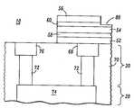
도 1을 참조로 하여, 본 발명은 상호접속 금속화(interconnect metallization)의 세 레벨들에서 형성된 예시적인 커패시터 구조의 형성 및 접속에 대하여 설명된다. 집적 회로 구조(10)의 일부분은 본 발명의 상세한 설명을 제공하기 위해 상호접속 금속화 구조의 부분적인 단면도가 도시된다. 금속화 구조는, 전형적으로 그 표면상에 다수의 트랜지스터들을 갖는 반도체 층(도시되지 않음) 상에 형성된다. 본 예시적인 실시예에서, Al 또는 Cu 러너들(runners)과 같은, 금속 상호접속의 몇몇 상위 레벨들이 다마신 제조 공정(Damascene fabrication process)에 따라서 반도체층 상에서 형성된다. 특히, 도 1에 도시된 집적 회로 구조(10)의 일부분은 3개의 연속하게 형성된 금속화의 레벨들(20, 30 및 40)을 포함한다. 금속화의 하나 이상의 부가적인 레벨들은 레벨(20) 아래에 형성되고, 금속화의 하나 이상의 부가적인 레벨들은 레벨(40) 아래에 형성된다. 일반적으로, 각 레벨의 금속 러너들은 레벨(20)을 따라 라인(42)에 의해 도시되는 것처럼 평면을 따라 형성된다. 본 발명을 설명하기 위한 목적으로, 커패시터 구조(50)는 설명된 금속화의 레벨들에서 도전체들과 전기적으로 접속된다. 커패시터 구조(50)는 평면(42) 또는 상기 구조가 형성되는 표면의 평면과 같은 기초 평면에 대하여 수직 정렬하여 형성된 교호하는 도전체(conductor) 및 절연체(insulator) 층을 포함한다. 상기 구조(50)는 두 개의 커패시터들을 평행하게 제공하도록 배선되어 있다. 세 개의 도전체 층들(52, 54 및 56)은 두 개의 개재 유전체 층들(intervening dielectric layers)에 의해 다른 것으로부터 절연된다. 하나의 유전체 층(58)은 도전체들(52 및 54) 사이에서 형성되고, 다른 유전체 층(60)은 도전체 층들(54 및 56) 사이에서 형성된다.With reference to FIG. 1, the present invention is described with respect to the formation and connection of an exemplary capacitor structure formed at three levels of interconnect metallization. Part of the
도시된 구조(50)에서, 도전체 층(54)은 층(52 및 58)으로 형성된 제 1 커패시터 및 층(56 및 60)으로 형성된 제 2 커패시터에서 공통인 커패시터 평면이다. 금속화 레벨(40)의 비어부(via portion)(64)는 두 커패시터들에 대한 공통 터미널을 제공하기 위해 도전체 층(54)과 접속한다. 금속화 레벨(40)의 또 다른 비어부(66)는 층(54, 56, 및 60)에 의해 형성되는 커패시터에 대한 제 2 터미널을 제공하기 위해 도전체 층(56)과 접속된다. 금속화 레벨(30)의 도전체 러너 부(68)는 층(52, 54, 58)에 의해 형성된 커패시터의 제 2 접속을 제공하기 위해 도전체 평면 층(52)에 접속을 제공한다.In the
금속화 레벨(30)의 비어부(72)는 금속화 레벨(20)의 도전성 러너(74)에 도전성 러너부(68)를 접속한다. 도전성 러너(74)는 다른 비어부(72)를 통하여 레벨(30)의 도전성 러너부(76)와 접속된다. 비어부(66)를 통해 커패시터 도전체(56)로의 접촉을 달성하기 위해, 레벨(40)의 비어부(78)는 도전성 러너부(76)와 레벨(40)의 도전성 러너(82)를 접속한다. (금속화의 오버라잉 레벨과 연관된)비어부(94)는 평면(52 및 56)과 도시되지 않은 다른 회로와의 접속을 제공한다. 대안적으로, 이 접속은 레벨(20)의 도전성 러너(74)를 통해 금속화의 더 낮은 레벨로 만들어 질 수 있다. (또한 금속화의 오버라잉 레벨에 또한 연관되는)비어부(96)는 레벨(40)의 도전성 러너(98)를 통해 공통 플레이트(54)의 도시되지 않은 다른 회로로의 접속을 제공한다.The
예시적인 커패시터(50)가 형성되는 다마신 구조(Damascene structure)는 잘 알려져 있고, 간단하게만 설명된다. 일반적으로, 예시적인 실시예들에서, 금속화의 각 레벨은 도 2의 층(70)과 같이 유전체 층의 최초의 증착과 함께 형성된다. 금속화의 레벨(20)은 커패시터 구조(50)의 형성 전에 완료된다. 유전체 재료의 층(70)은 전형적으로 다중 층이고, 실리콘 질화물과 같은 에칭 스톱과 함께 형성되고, CMP(chemical mechanical polishing)에 의해 평면화된다. Cu 도전체 라인들의 요구된 구성들은 트렌치-형 구멍(trench-like openings)을 형성하기 위해 유전체 재료로 패터닝되고 에칭된다. 일반적으로, Ta, TaN 또는 TiN과 같은 도전성 장벽 재료는 그 후에 구멍에 증착되는 구리의 이동을 방지하기 위해 에칭된 구멍의 표면을 따라 증착된다. 장벽 금속은 화학적 증기 증착(CVD) 또는 물리적 증기 증착(PVD)과 함께 형성될 것이다.The damascene structure in which the
Cu 증착은 구멍들을 채우기 위해,[예를 들면, 구리 황산염(Copper sulfate)으로부터] Cu의 전기-플레팅에 의하여, 장벽 재료상의 시드 층(seed layer)의 증착과 함께 시작된다. 도시된 레벨(20)의 이중 다마신 구조에 대하여, 비어부(금속화의 다른 레벨 사이에서 접속을 제공한다) 및 도전체 부(금속화 레벨의 도전체 러너들을 제공한다)는 연속적인 패턴 및 에칭 단계들에서 형성되고, 장벽층 재료, 시드층의 증착에 의해 계속되고, Cu의 전기 증착은 비어부들 및 구멍의 도전체 부재부들(member portions)을 채우는 것을 완료한다. Cu 증착 후에, 가열 냉각(anneal)은 마이크로 구조를 안정화하기 위해 제공될 것이다. 상기 구조는 유전체 층(70)의 표면으로부터 초과 구리 및 장벽 재료를 제거하기 위해 폴리싱(polishing)된다. 이 시퀀스는 상호접속의 마지막 구리층이 페시베이트(passivate)될 때까지 금속화의 각각의 레벨에 대하여 반복되고, 구조는 패키징 및 조립을 위해 준비된다.Cu deposition commences with the deposition of a seed layer on the barrier material by electro-plating Cu (eg, from copper sulfate) to fill the pores. For the dual damascene structure of the
일단 이중 다마신 레벨(20)이 도전체(52, 54 및 56)의 층들을 완료하면, 개재 유전체 층들(58 및 60)이 증착된다. 도 3을 참조하라. 도전체 층들(52, 54, 54)은 스프터링된 Ta 또는 TaN 또는 TiN으로 형성될 것이다. 이러한 층들은 물리적 증기 증착(PDV) 또는 화학적 증기 증착(CVD)에 의해 증착될 것이다. 양호하게, 도전체 층(52)은 확산 장벽을 제공하도록 Ti/TiN 또는 Ta/TaN 스택을 포함하고, 하부 유전체 층(70)과 함께 도전체 층(52)의 적절한 부착(adhesion)을 보장한다. 예를 들면, 약 20nm의 Ti 및 약 40nm의 TiN을 갖는 Ti/TiN 스택은 가열 냉각에 따른 400C의 연속적인 스프터링에 의해 증착될 것이다. 층들(54 및 56)은 또한 식별된 재료들의 스프터링 기술들에 의해 또한 증착될 것이다. 그러나, 폭넓게 다양한 다른 도전성 재료들이 적합할 것이다. 유전체 층들(58 및 60)은 CVD에 의해 증착된 실리콘 산화물일 것이다. 산화물(oxide)은 실란(silane)으로부터 형성될 것이다. 대안적으로, 유전체 층들(58 및 60)은 TaO5로 형성될 것이다. 다른 절연체 재료들은 요구된 유전체 특성들 및 최소 전류 손실을 관한 요구를 기본으로 하여 선택될 것이다.Once the
도 4 및 5를 참조로 하여, 최상위 도전체 층(56)은 그 일부를 제거하기 위하여 패터닝되고 에칭되며, 하부 층(54)과 전기적 접속을 제공하기 위해 구멍(88)을 형성한다. 구멍(88)이 층(54)과의 접속을 위해 층(56)을 통해 형성된 후에, 모든 층들(52, 54, 56, 58 및 60)들은 도전체 구조(50)를 전체적으로 정의하도록 수직 정렬하여 패터닝되고 에칭된다. 즉, 에칭은 구조(50)가 형성되는 평면(42) 또는 유전체 층(70)의 표면을 따른 평면과 같은 기초 평면에 대해 수직으로 배열된 층들을 정의한다. 다음 도 6을 보면, 층들(52, 54, 56, 58 및 60) 뿐 아니라 유전체 층(70)의 노출된 부분 상에 증착된 실리콘 60 nm 질화물의 장벽층(80)과 금속화 레벨(20)의 Cu의 노출된 영역이 도시되어 있다(도 5를 참조하라).4 and 5, the
도 6을 참조하여, 다른 유전체 층(90)은 HDP(high density plasma)와 같은 컨포멀 증착(conformal deposition)에 의해 구조(10) 상에 형성된다. 유전체 층(90)은 CMP 또는 MTR(metal topographic reduction)에 의해 평면화 되고, 낮은 영역들 상의 포토레지스트의 증착은 표준 에칭에 의해 행해진다. 금속화 레벨(40)의 형성을 위해 준비된 평면화된 구조는 도 7에 도시된다.Referring to FIG. 6, another
금속화 레벨(40)의 비어부들(64 및 66) 및 도전체 부재들(82 및 98)은 도 1에 도시된 것처럼 유전체 층(90) 상에 형성된다.
커패시터 구조(50)는 도 8에 도시된 것과 같은 회로 구조(10)에서 상호접속 도전체의 두 레벨들과 또한 접속될 것이다. 더 낮은 도전체 레벨(30)은 더 낮은 평면(52) 및 레벨(40)의 비어부(92) 사이의 효과적인 접속을 위한 러너부(124)를 포함한다. 다른 접속들은 도 1을 참조하여 설명된 것과 같다.
3개의 스택들에 대한 또 다른 실시예에서, 셋, 넷, 및 그 이상의 커패시터들은 도전체의 두 레벨들 사이에서 형성되는 스택들의 평행한 접속으로 제조 될 수 있다. 도 9는 커패시터 유전체들을 제공하게 위해 한 쌍의 층들(120) 사이에 위치된 개재 유전체 층들(124)이 연속적으로 증착된 5개의 도전체 층들(122)을 포함하는 스택을 도시한다. 각각의 층들(122)로의 접속은 평행하게 접속된 4개의 커패시터들을 구성하기 위해서 비어부(126) 및 도전성 러너들(120, 123 및 124)을 통해 만들어진다.In another embodiment for three stacks, three, four, and more capacitors can be fabricated with parallel connections of stacks formed between two levels of conductor. 9 shows a stack comprising five
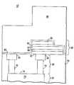
이중 다마신 실시예들에서 보여지는 원리는, 또한 종래의 감산 금속 에치 공정(subtractive metal etch process)의 Al 상호 접속에 쉽게 인가될 수 있다. 도 10에는 커패시터 유전체를 제공하기 위한 층들의 쌍들[(252, 254) 및 (254, 246)] 사이에 위치되는 두 개의 개재 유전체 층들(262)을 갖는 3개의 연속적으로 형성된 금속층(252, 254, 246)을 포함하는 커패시터 구조(250)를 도시한다. 구조(250)는 두 개의 평행한 커패시터를 구성하기 위해 접속된다. 가장 낮은 레벨(252) 금속층은 접속을 제공하는 Ti/TiN의 아래층 및 확산에 반하는 장벽과 함께 Al-Cu 합금을 포함하는 Al 상호접속의 레벨(270)의 러너일 것이다. 레벨(270)은 유전체 층(272)상에 형성된다. 층(254 및 256)은 증착된 TiN 일 것이다. Al 상호접속의 제 2 레벨(280)은 유전체 층(284) 내에 구조(250)상에서 형성된다. 접속들(286)은 레벨(280)의 두 개의 러너(290 및 292)와 접속되는 평행한 커패시터들을 구성하기 위해서 층간 유전체 층(288)을 통해 확장된다. 대안적으로, 커패시터 구조(250)의 모든 층들은 수직 정렬하여 형성되고, 레벨(270)(도시되지 않음) 아래의 금속 러너로의 접속을 통해 러너(290) 및 층(252) 사의의 접속이 이루어진다.The principle shown in the dual damascene embodiments can also be readily applied to the Al interconnect of a conventional subtractive metal etch process. 10 shows three consecutively formed
구조는 집적 회로들 내의 커패시터 구조들의 고밀도 형성에 대하여 유용하게 설명되었다. 개시된 디자인 및 제작 방법들의 어플리케이션은 많은 양의 정전용량을 요구하는 커패시터들 및 아날로그 회로를 이용하는 메모리 회로들을 포함하 는, 디지털 및 아날로그 회로 어플리케이션들의 변화를 만들 것이다. 개시된 특정한 금속 및 절연 재료는 평행한 커패시터들의 구성을 위해 도시된 특정 상호접속 패턴들과 같은 예시이다. 그러나 본 명세서에 개시된 원리는 화합물 구조와 같은 다른 재료들로 형성된 구조를 포함하는, 다양한 회로 구조들상의 다양한 방법들로 본 발명을 실행하기 위한 기조를 제공한다, 다양한 변형은 당업자에 의해 명백해 질 것이다. 그러므로, 본 명세서에 설명되지 않았다 할 지라고 다른 구성들은 다음의 청구항에 의해서만 제한되는 본 발명의 영역에서 벗어나지 않는다.The structure has been usefully described for the high density formation of capacitor structures in integrated circuits. Applications of the disclosed design and fabrication methods will make changes in digital and analog circuit applications, including memory circuits using analog circuits and capacitors requiring large amounts of capacitance. The particular metals and insulating materials disclosed are examples such as the particular interconnect patterns shown for the construction of parallel capacitors. However, the principles disclosed herein provide a basis for practicing the invention in a variety of ways on various circuit structures, including structures formed of other materials, such as compound structures, various modifications will become apparent to those skilled in the art. . Therefore, other configurations, whether or not described herein, do not depart from the scope of the invention, which is limited only by the following claims.
본 발명에 의하면, 반도체 층상에 금속화 레벨들로 형성된 커패시터 구조들을 갖는 디바이스들이 제공된다.
According to the present invention, devices having capacitor structures formed in metallization levels on a semiconductor layer are provided.
Claims (10)
Translated fromKoreanApplications Claiming Priority (2)
| Application Number | Priority Date | Filing Date | Title |
|---|---|---|---|
| US09/653,295 | 2000-08-31 | ||
| US09/653,295US6838717B1 (en) | 2000-08-31 | 2000-08-31 | Stacked structure for parallel capacitors and method of fabrication |
Publications (2)
| Publication Number | Publication Date |
|---|---|
| KR20020018603A KR20020018603A (en) | 2002-03-08 |
| KR100773256B1true KR100773256B1 (en) | 2007-11-05 |
Family
ID=24620268
Family Applications (1)
| Application Number | Title | Priority Date | Filing Date |
|---|---|---|---|
| KR1020010053297AExpired - LifetimeKR100773256B1 (en) | 2000-08-31 | 2001-08-31 | Stacked structure for parallel capacitors and method of fabrication |
Country Status (5)
| Country | Link |
|---|---|
| US (1) | US6838717B1 (en) |
| JP (1) | JP2002141417A (en) |
| KR (1) | KR100773256B1 (en) |
| GB (1) | GB2371147B (en) |
| TW (1) | TW515099B (en) |
Families Citing this family (28)
| Publication number | Priority date | Publication date | Assignee | Title |
|---|---|---|---|---|
| US6498364B1 (en)* | 2000-01-21 | 2002-12-24 | Agere Systems Inc. | Capacitor for integration with copper damascene processes |
| US6784478B2 (en) | 2002-09-30 | 2004-08-31 | Agere Systems Inc. | Junction capacitor structure and fabrication method therefor in a dual damascene process |
| KR100480641B1 (en)* | 2002-10-17 | 2005-03-31 | 삼성전자주식회사 | Metal-Insulator-Metal capacitor having high capacitance, integrated circuit chip having the same and method for manufacturing the same |
| JP2004179419A (en) | 2002-11-27 | 2004-06-24 | Toshiba Corp | Semiconductor device and manufacturing method thereof |
| KR100505658B1 (en)* | 2002-12-11 | 2005-08-03 | 삼성전자주식회사 | Semiconductor device having MIM capacitor |
| DE10260352A1 (en)* | 2002-12-20 | 2004-07-15 | Infineon Technologies Ag | Method of manufacturing a capacitor arrangement and capacitor arrangement |
| US6680521B1 (en)* | 2003-04-09 | 2004-01-20 | Newport Fab, Llc | High density composite MIM capacitor with reduced voltage dependence in semiconductor dies |
| US6777777B1 (en)* | 2003-05-28 | 2004-08-17 | Newport Fab, Llc | High density composite MIM capacitor with flexible routing in semiconductor dies |
| US20050116276A1 (en)* | 2003-11-28 | 2005-06-02 | Jing-Horng Gau | Metal-insulator-metal (MIM) capacitor and fabrication method for making the same |
| KR100549002B1 (en)* | 2004-02-04 | 2006-02-02 | 삼성전자주식회사 | Semiconductor device having multilayer M capacitor and method of manufacturing same |
| US7535079B2 (en)* | 2005-06-09 | 2009-05-19 | Freescale Semiconductor, Inc. | Semiconductor device comprising passive components |
| US6919244B1 (en)* | 2004-03-10 | 2005-07-19 | Motorola, Inc. | Method of making a semiconductor device, and semiconductor device made thereby |
| KR100695993B1 (en)* | 2004-12-30 | 2007-03-15 | 매그나칩 반도체 유한회사 | Multi-Layered MMC Capacitor and Manufacturing Method Thereof |
| US20070057305A1 (en)* | 2005-09-13 | 2007-03-15 | Taiwan Semiconductor Manufacturing Company, Ltd. | MIM capacitor integrated into the damascene structure and method of making thereof |
| KR100678638B1 (en)* | 2005-11-08 | 2007-02-05 | 삼성전자주식회사 | Manufacturing Method of Semiconductor Device |
| US7964470B2 (en) | 2006-03-01 | 2011-06-21 | Taiwan Semiconductor Manufacturing Company, Ltd. | Flexible processing method for metal-insulator-metal capacitor formation |
| US8124490B2 (en)* | 2006-12-21 | 2012-02-28 | Stats Chippac, Ltd. | Semiconductor device and method of forming passive devices |
| KR100902581B1 (en)* | 2007-10-16 | 2009-06-11 | 주식회사 동부하이텍 | Stack Capacitors in Semiconductor Devices and Methods of Forming Them |
| KR100957881B1 (en) | 2007-12-28 | 2010-05-13 | 매그나칩 반도체 유한회사 | MIM Capacitor |
| US7602599B1 (en)* | 2008-07-09 | 2009-10-13 | United Microelectronics Corp. | Metal-metal capacitor and method of making the same |
| KR101036744B1 (en)* | 2009-01-29 | 2011-05-24 | 주식회사 하이닉스반도체 | Manufacturing Method of Semiconductor Memory Device |
| US7951663B2 (en)* | 2009-05-26 | 2011-05-31 | Stats Chippac, Ltd. | Semiconductor device and method of forming IPD structure using smooth conductive layer and bottom-side conductive layer |
| US9041148B2 (en)* | 2013-06-13 | 2015-05-26 | Qualcomm Incorporated | Metal-insulator-metal capacitor structures |
| CN105304615B (en) | 2014-06-05 | 2018-03-23 | 联华电子股份有限公司 | Semiconductor structure |
| WO2016136411A1 (en)* | 2015-02-27 | 2016-09-01 | 株式会社村田製作所 | Capacitor and electronic device |
| US9761655B1 (en) | 2016-06-20 | 2017-09-12 | International Business Machines Corporation | Stacked planar capacitors with scaled EOT |
| US11222945B2 (en)* | 2017-12-29 | 2022-01-11 | Texas Instruments Incorporated | High voltage isolation structure and method |
| JP2021077799A (en)* | 2019-11-12 | 2021-05-20 | ローム株式会社 | Electronic component |
Citations (3)
| Publication number | Priority date | Publication date | Assignee | Title |
|---|---|---|---|---|
| KR940027163A (en)* | 1993-05-21 | 1994-12-10 | 야마자끼 순뻬이 | Hybrid integrated circuit components |
| JPH07111318A (en)* | 1993-10-12 | 1995-04-25 | Olympus Optical Co Ltd | Ferroelectric memory |
| US5736448A (en)* | 1995-12-04 | 1998-04-07 | General Electric Company | Fabrication method for thin film capacitors |
Family Cites Families (7)
| Publication number | Priority date | Publication date | Assignee | Title |
|---|---|---|---|---|
| US3962713A (en)* | 1972-06-02 | 1976-06-08 | Texas Instruments Incorporated | Large value capacitor |
| US5583359A (en)* | 1995-03-03 | 1996-12-10 | Northern Telecom Limited | Capacitor structure for an integrated circuit |
| US5926359A (en)* | 1996-04-01 | 1999-07-20 | International Business Machines Corporation | Metal-insulator-metal capacitor |
| US6066537A (en)* | 1998-02-02 | 2000-05-23 | Tritech Microelectronics, Ltd. | Method for fabricating a shielded multilevel integrated circuit capacitor |
| US6180976B1 (en)* | 1999-02-02 | 2001-01-30 | Conexant Systems, Inc. | Thin-film capacitors and methods for forming the same |
| WO2000049660A1 (en)* | 1999-02-16 | 2000-08-24 | Symetrix Corporation | Iridium oxide diffusion barrier between local interconnect layer and thin film of layered superlattice material |
| JP3950290B2 (en)* | 1999-09-10 | 2007-07-25 | 三星電子株式会社 | Semiconductor memory device including capacitor protective film and method of manufacturing the same |
- 2000
- 2000-08-31USUS09/653,295patent/US6838717B1/ennot_activeExpired - Lifetime
- 2001
- 2001-08-30TWTW090121470Apatent/TW515099B/ennot_activeIP Right Cessation
- 2001-08-31GBGB0121201Apatent/GB2371147B/ennot_activeExpired - Fee Related
- 2001-08-31JPJP2001262599Apatent/JP2002141417A/ennot_activeWithdrawn
- 2001-08-31KRKR1020010053297Apatent/KR100773256B1/ennot_activeExpired - Lifetime
Patent Citations (5)
| Publication number | Priority date | Publication date | Assignee | Title |
|---|---|---|---|---|
| KR940027163A (en)* | 1993-05-21 | 1994-12-10 | 야마자끼 순뻬이 | Hybrid integrated circuit components |
| US5643804A (en)* | 1993-05-21 | 1997-07-01 | Semiconductor Energy Laboratory Co., Ltd. | Method of manufacturing a hybrid integrated circuit component having a laminated body |
| JPH07111318A (en)* | 1993-10-12 | 1995-04-25 | Olympus Optical Co Ltd | Ferroelectric memory |
| US5481490A (en)* | 1993-10-12 | 1996-01-02 | Olympus Optical Co., Ltd. | Ferroelectric memory |
| US5736448A (en)* | 1995-12-04 | 1998-04-07 | General Electric Company | Fabrication method for thin film capacitors |
Also Published As
| Publication number | Publication date |
|---|---|
| GB0121201D0 (en) | 2001-10-24 |
| JP2002141417A (en) | 2002-05-17 |
| GB2371147B (en) | 2005-04-13 |
| GB2371147A (en) | 2002-07-17 |
| KR20020018603A (en) | 2002-03-08 |
| US6838717B1 (en) | 2005-01-04 |
| TW515099B (en) | 2002-12-21 |
Similar Documents
| Publication | Publication Date | Title |
|---|---|---|
| KR100773256B1 (en) | Stacked structure for parallel capacitors and method of fabrication | |
| JP3790469B2 (en) | Semiconductor device | |
| US6426249B1 (en) | Buried metal dual damascene plate capacitor | |
| EP0852065B1 (en) | Interconnect scheme for integrated circuits | |
| US6639298B2 (en) | Multi-layer inductor formed in a semiconductor substrate | |
| US7709905B2 (en) | Dual damascene wiring and method | |
| CN1194418C (en) | Integrated component comprising metal-insulator-metal capacitor | |
| JP4386680B2 (en) | Capacitor for semiconductor device and manufacturing method thereof | |
| US20070155147A1 (en) | Semiconductor device and method for fabricating the same | |
| JPH08213397A (en) | Semiconductor device with damask metallized structure | |
| US11769722B2 (en) | Method of forming a metal-insulator-metal (MIM) capacitor | |
| CN100416818C (en) | Semiconductor device and manufacturing method thereof | |
| KR100806034B1 (en) | Semiconductor device having MIM capacitor and manufacturing method thereof | |
| US6387750B1 (en) | Method of forming MIM capacitor | |
| US9177908B2 (en) | Stacked semiconductor capacitor structure | |
| US20090149019A1 (en) | Semiconductor device and method for fabricating the same | |
| US6734483B2 (en) | Process for fabricating a capacitor within an integrated circuit, and corresponding integrated circuit | |
| JP4034482B2 (en) | Multilayer wiring structure and method of manufacturing semiconductor device | |
| EP2738827B1 (en) | MIMCAP structure in a semiconductor device package | |
| US20050112957A1 (en) | Partial inter-locking metal contact structure for semiconductor devices and method of manufacture | |
| EP1378935A2 (en) | A method to form both high and low-K materials in one plane on a substrate, and their application in mixed mode circuits | |
| WO2007041504A1 (en) | High density, high q capacitor on top of protective layer | |
| US7169680B2 (en) | Method for fabricating a metal-insulator-metal capacitor | |
| CN100373546C (en) | Method for manufacturing metal-insulating layer-metal capacitor | |
| TW583752B (en) | Method of forming MIM capacitor integrated with damascene process |
Legal Events
| Date | Code | Title | Description |
|---|---|---|---|
| PA0109 | Patent application | Patent event code:PA01091R01D Comment text:Patent Application Patent event date:20010831 | |
| PG1501 | Laying open of application | ||
| A201 | Request for examination | ||
| PA0201 | Request for examination | Patent event code:PA02012R01D Patent event date:20060831 Comment text:Request for Examination of Application Patent event code:PA02011R01I Patent event date:20010831 Comment text:Patent Application | |
| E701 | Decision to grant or registration of patent right | ||
| PE0701 | Decision of registration | Patent event code:PE07011S01D Comment text:Decision to Grant Registration Patent event date:20070808 | |
| GRNT | Written decision to grant | ||
| PR0701 | Registration of establishment | Comment text:Registration of Establishment Patent event date:20071030 Patent event code:PR07011E01D | |
| PR1002 | Payment of registration fee | Payment date:20071031 End annual number:3 Start annual number:1 | |
| PG1601 | Publication of registration | ||
| PR1001 | Payment of annual fee | Payment date:20101026 Start annual number:4 End annual number:4 | |
| PR1001 | Payment of annual fee | Payment date:20111025 Start annual number:5 End annual number:5 | |
| FPAY | Annual fee payment | Payment date:20121009 Year of fee payment:6 | |
| PR1001 | Payment of annual fee | Payment date:20121009 Start annual number:6 End annual number:6 | |
| FPAY | Annual fee payment | Payment date:20131001 Year of fee payment:7 | |
| PR1001 | Payment of annual fee | Payment date:20131001 Start annual number:7 End annual number:7 | |
| FPAY | Annual fee payment | Payment date:20141006 Year of fee payment:8 | |
| PR1001 | Payment of annual fee | Payment date:20141006 Start annual number:8 End annual number:8 | |
| FPAY | Annual fee payment | Payment date:20180330 Year of fee payment:11 | |
| PR1001 | Payment of annual fee | Payment date:20180330 Start annual number:11 End annual number:11 | |
| FPAY | Annual fee payment | Payment date:20181015 Year of fee payment:12 | |
| PR1001 | Payment of annual fee | Payment date:20181015 Start annual number:12 End annual number:12 | |
| FPAY | Annual fee payment | Payment date:20191001 Year of fee payment:13 | |
| PR1001 | Payment of annual fee | Payment date:20191001 Start annual number:13 End annual number:13 | |
| PC1801 | Expiration of term | Termination date:20220228 Termination category:Expiration of duration |