KR100772836B1 - Manufacturing Method of Semiconductor Device - Google Patents
Manufacturing Method of Semiconductor DeviceDownload PDFInfo
- Publication number
- KR100772836B1 KR100772836B1KR1020060068303AKR20060068303AKR100772836B1KR 100772836 B1KR100772836 B1KR 100772836B1KR 1020060068303 AKR1020060068303 AKR 1020060068303AKR 20060068303 AKR20060068303 AKR 20060068303AKR 100772836 B1KR100772836 B1KR 100772836B1
- Authority
- KR
- South Korea
- Prior art keywords
- poly
- semiconductor substrate
- stress
- poly layer
- layer
- Prior art date
- Legal status (The legal status is an assumption and is not a legal conclusion. Google has not performed a legal analysis and makes no representation as to the accuracy of the status listed.)
- Expired - Fee Related
Links
Images


Classifications
- H—ELECTRICITY
- H01—ELECTRIC ELEMENTS
- H01L—SEMICONDUCTOR DEVICES NOT COVERED BY CLASS H10
- H01L21/00—Processes or apparatus adapted for the manufacture or treatment of semiconductor or solid state devices or of parts thereof
- H01L21/02—Manufacture or treatment of semiconductor devices or of parts thereof
- H01L21/04—Manufacture or treatment of semiconductor devices or of parts thereof the devices having potential barriers, e.g. a PN junction, depletion layer or carrier concentration layer
- H01L21/18—Manufacture or treatment of semiconductor devices or of parts thereof the devices having potential barriers, e.g. a PN junction, depletion layer or carrier concentration layer the devices having semiconductor bodies comprising elements of Group IV of the Periodic Table or AIIIBV compounds with or without impurities, e.g. doping materials
- H01L21/26—Bombardment with radiation
- H01L21/263—Bombardment with radiation with high-energy radiation
- H01L21/265—Bombardment with radiation with high-energy radiation producing ion implantation
- H01L21/26506—Bombardment with radiation with high-energy radiation producing ion implantation in group IV semiconductors
- H—ELECTRICITY
- H01—ELECTRIC ELEMENTS
- H01L—SEMICONDUCTOR DEVICES NOT COVERED BY CLASS H10
- H01L21/00—Processes or apparatus adapted for the manufacture or treatment of semiconductor or solid state devices or of parts thereof
- H01L21/02—Manufacture or treatment of semiconductor devices or of parts thereof
- H01L21/04—Manufacture or treatment of semiconductor devices or of parts thereof the devices having potential barriers, e.g. a PN junction, depletion layer or carrier concentration layer
- H01L21/18—Manufacture or treatment of semiconductor devices or of parts thereof the devices having potential barriers, e.g. a PN junction, depletion layer or carrier concentration layer the devices having semiconductor bodies comprising elements of Group IV of the Periodic Table or AIIIBV compounds with or without impurities, e.g. doping materials
- H01L21/26—Bombardment with radiation
- H01L21/263—Bombardment with radiation with high-energy radiation
- H01L21/265—Bombardment with radiation with high-energy radiation producing ion implantation
- H01L21/26586—Bombardment with radiation with high-energy radiation producing ion implantation characterised by the angle between the ion beam and the crystal planes or the main crystal surface
- H—ELECTRICITY
- H01—ELECTRIC ELEMENTS
- H01L—SEMICONDUCTOR DEVICES NOT COVERED BY CLASS H10
- H01L21/00—Processes or apparatus adapted for the manufacture or treatment of semiconductor or solid state devices or of parts thereof
- H01L21/02—Manufacture or treatment of semiconductor devices or of parts thereof
- H01L21/04—Manufacture or treatment of semiconductor devices or of parts thereof the devices having potential barriers, e.g. a PN junction, depletion layer or carrier concentration layer
- H01L21/18—Manufacture or treatment of semiconductor devices or of parts thereof the devices having potential barriers, e.g. a PN junction, depletion layer or carrier concentration layer the devices having semiconductor bodies comprising elements of Group IV of the Periodic Table or AIIIBV compounds with or without impurities, e.g. doping materials
- H01L21/28—Manufacture of electrodes on semiconductor bodies using processes or apparatus not provided for in groups H01L21/20 - H01L21/268
- H01L21/28008—Making conductor-insulator-semiconductor electrodes
- H01L21/28017—Making conductor-insulator-semiconductor electrodes the insulator being formed after the semiconductor body, the semiconductor being silicon
- H01L21/28026—Making conductor-insulator-semiconductor electrodes the insulator being formed after the semiconductor body, the semiconductor being silicon characterised by the conductor
- H01L21/28035—Making conductor-insulator-semiconductor electrodes the insulator being formed after the semiconductor body, the semiconductor being silicon characterised by the conductor the final conductor layer next to the insulator being silicon, e.g. polysilicon, with or without impurities
- H—ELECTRICITY
- H10—SEMICONDUCTOR DEVICES; ELECTRIC SOLID-STATE DEVICES NOT OTHERWISE PROVIDED FOR
- H10D—INORGANIC ELECTRIC SEMICONDUCTOR DEVICES
- H10D30/00—Field-effect transistors [FET]
- H10D30/60—Insulated-gate field-effect transistors [IGFET]
- H10D30/791—Arrangements for exerting mechanical stress on the crystal lattice of the channel regions
- H10D30/794—Arrangements for exerting mechanical stress on the crystal lattice of the channel regions comprising conductive materials, e.g. silicided source, drain or gate electrodes
- H—ELECTRICITY
- H10—SEMICONDUCTOR DEVICES; ELECTRIC SOLID-STATE DEVICES NOT OTHERWISE PROVIDED FOR
- H10D—INORGANIC ELECTRIC SEMICONDUCTOR DEVICES
- H10D64/00—Electrodes of devices having potential barriers
- H10D64/60—Electrodes characterised by their materials
- H10D64/66—Electrodes having a conductor capacitively coupled to a semiconductor by an insulator, e.g. MIS electrodes
- H10D64/661—Electrodes having a conductor capacitively coupled to a semiconductor by an insulator, e.g. MIS electrodes the conductor comprising a layer of silicon contacting the insulator, e.g. polysilicon having vertical doping variation
- H10D64/662—Electrodes having a conductor capacitively coupled to a semiconductor by an insulator, e.g. MIS electrodes the conductor comprising a layer of silicon contacting the insulator, e.g. polysilicon having vertical doping variation the conductor further comprising additional layers, e.g. multiple silicon layers having different crystal structures
- H—ELECTRICITY
- H10—SEMICONDUCTOR DEVICES; ELECTRIC SOLID-STATE DEVICES NOT OTHERWISE PROVIDED FOR
- H10D—INORGANIC ELECTRIC SEMICONDUCTOR DEVICES
- H10D84/00—Integrated devices formed in or on semiconductor substrates that comprise only semiconducting layers, e.g. on Si wafers or on GaAs-on-Si wafers
- H10D84/01—Manufacture or treatment
- H10D84/0123—Integrating together multiple components covered by H10D12/00 or H10D30/00, e.g. integrating multiple IGBTs
- H10D84/0126—Integrating together multiple components covered by H10D12/00 or H10D30/00, e.g. integrating multiple IGBTs the components including insulated gates, e.g. IGFETs
- H10D84/0165—Integrating together multiple components covered by H10D12/00 or H10D30/00, e.g. integrating multiple IGBTs the components including insulated gates, e.g. IGFETs the components including complementary IGFETs, e.g. CMOS devices
- H10D84/0167—Manufacturing their channels
- H—ELECTRICITY
- H10—SEMICONDUCTOR DEVICES; ELECTRIC SOLID-STATE DEVICES NOT OTHERWISE PROVIDED FOR
- H10D—INORGANIC ELECTRIC SEMICONDUCTOR DEVICES
- H10D84/00—Integrated devices formed in or on semiconductor substrates that comprise only semiconducting layers, e.g. on Si wafers or on GaAs-on-Si wafers
- H10D84/01—Manufacture or treatment
- H10D84/02—Manufacture or treatment characterised by using material-based technologies
- H10D84/03—Manufacture or treatment characterised by using material-based technologies using Group IV technology, e.g. silicon technology or silicon-carbide [SiC] technology
- H10D84/038—Manufacture or treatment characterised by using material-based technologies using Group IV technology, e.g. silicon technology or silicon-carbide [SiC] technology using silicon technology, e.g. SiGe
Landscapes
- Physics & Mathematics (AREA)
- Engineering & Computer Science (AREA)
- High Energy & Nuclear Physics (AREA)
- Condensed Matter Physics & Semiconductors (AREA)
- General Physics & Mathematics (AREA)
- Manufacturing & Machinery (AREA)
- Computer Hardware Design (AREA)
- Microelectronics & Electronic Packaging (AREA)
- Power Engineering (AREA)
- Health & Medical Sciences (AREA)
- Toxicology (AREA)
- Chemical & Material Sciences (AREA)
- Crystallography & Structural Chemistry (AREA)
- Insulated Gate Type Field-Effect Transistor (AREA)
- Drying Of Semiconductors (AREA)
Abstract
Translated fromKoreanDescription
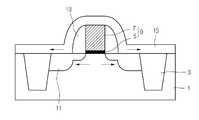
Translated fromKorean도 1은 종래에 이동도 증가를 위해 배리어층에 스트레스를 부가한 반도체소자의 단면도를 나타낸 도면.1 is a cross-sectional view of a semiconductor device in which a stress is applied to a barrier layer in order to increase mobility.
도 2a 내지 도 2f는 본 발명의 실시예에 따른 반도체소자의 제조 공정을 설명한 도면.2A to 2F illustrate a manufacturing process of a semiconductor device according to an embodiment of the present invention.
도 3은 도 2c와 같이 식각하지 않은 상태로 이온 주입하는 경우, 스트레스 불량을 도시한 도면.3 is a view showing a stress failure when the ion implanted in a non-etched state as shown in Figure 2c.
<도면의 주요 부분에 대한 부호의 설명><Explanation of symbols for main parts of the drawings>
21: 반도체 기판 23: 소자 분리 영역21: semiconductor substrate 23: device isolation region
25: 폴리층 27: 포토레지스트 패턴25
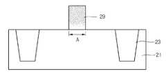
29: 폴리 D: 폴리층의 두께29: poly D: thickness of the poly layer
d: 깊이 A: 채널 영역d: depth A: channel area
본 발명은 반도체소자에 관한 것으로, 특히 소자 특성을 향상시킬 수 있는 반도체소자의 제조 방법에 관한 것이다.BACKGROUND OF THE
반도체소자가 고집적화됨에 따라서 소자활성영역의 크기와 소자활성영역 내에 형성되는 모스 트랜지스터(MOS transistor)의 채널 길이 모두 줄어들게 되었다.As semiconductor devices are highly integrated, both the size of the device active region and the channel length of the MOS transistors formed in the device active region are reduced.
이와 같이, 모스 트랜지스터의 채널 길이가 줄어듦에 따라 상기 채널 길이 내에서 전자의 충돌 확률이 증가하게 되어 결국 이동도(mobility)가 감소하게 된다.As described above, as the channel length of the MOS transistor decreases, collision probability of electrons increases in the channel length, resulting in reduced mobility.
따라서 전자의 이동도를 증가시키기 위해서는 전자의 충돌 확률을 감소시켜야 한다.Therefore, in order to increase the mobility of the electrons, the collision probability of the electrons must be reduced.
이러한 문제를 해결하기 위해 종래에는 도 1에 도시한 바와 같이, 에치 스탑(etch stop)으로 사용되는 배리어층(barrier layer, 15)에 스트레스를 부가하여 소자의 이동도를 증가시키는 방법이 제시되었다.In order to solve this problem, as shown in FIG. 1, a method of increasing the mobility of a device by adding a stress to a
이를 상세히 설명하면, 반도체 기판(1) 상에 소자 분리 영역(3)을 형성하고, 산화막(5)과 폴리(7)로 이루어진 게이트(9)를 형성하고, 상기 게이트(9)를 마스크로 하여 소자활성영역 내에 불순물 영역(11), 예컨대 소오스 영역 또는 드레인 영역을 형성하고, 상기 게이트(9)의 측면에 스페이서(13)를 형성한다.In detail, the
이후, 상기 반도체 기판(1)의 전면에 배리어층(15)을 형성한다. 상기 배리어층(15)으로는 SiN가 사용될 수 있다. 이때, 상기 배리어층(15)에 스트레스(stress)를 부가한다.Thereafter, the
이러한 경우, 상기 배리어층(15)은 게이트(9)를 기준으로 양 방향으로 스트 레스로 인한 장력(tensile force)이 발생하고, 이러한 장력에 의해 채널 또한 양 방향으로 장력이 발생한다. 이에 따라, 채널의 원자, 예컨대 Si의 격자 간의 거리가 넓어지게 되므로, 전자가 Si와 충돌할 확률이 줄어들게 된다.In this case, the
그러므로 소자의 이동도가 증가하게 되어 결국 소자의 특성이 향상될 수 있다.Therefore, the mobility of the device is increased, and thus the device characteristics may be improved.
채널에 스트레스로 인한 장력을 증가시키기 위해서는 배리어층(15)의 장력이 커져야 하는데, 배리어층(15)의 장력을 키우기 위해서는 배리어층의 두께를 증가시켜야 한다.In order to increase the tension due to stress in the channel, the tension of the
하지만, 배리어층(15)의 두께를 증가시키게 되는 경우, 콘택 오픈(contact open)을 위한 에칭시 배리어층이 오픈되지 않게 될 수 있다.However, when the thickness of the
따라서 결국, 배리어층(15)의 두께를 증가시키는 데에는 한계가 존재하고, 이러한 한계에 의해 이동도의 증가 또한 한계가 존재한다.Therefore, in the end, there is a limit in increasing the thickness of the
따라서 종래의 반도체 소자는 이동도의 증가에 한계가 존재하여 소자 특성을 현저하게 향상시킬 수 없게 문제점이 있다.Therefore, the conventional semiconductor device has a problem in that there is a limit to the increase in mobility, so that the device characteristics cannot be significantly improved.
따라서 본 발명은 폴리에 부가된 스트레스를 이용하여 소자의 이동도를 증가시켜 소자 특성을 현저하게 향상시킬 수 있는 반도체소자의 제조 방법을 제공함에 그 목적이 있다.Accordingly, an object of the present invention is to provide a method for manufacturing a semiconductor device that can significantly improve device characteristics by increasing the mobility of the device by using the stress added to the poly.
상기 목적을 달성하기 위한 본 발명의 제1 실시예에 따르면, 반도체소자의 제조 방법은, 반도체 기판상에 소정의 두께를 갖는 폴리층을 형성하는 단계; 포토레지스트 패턴을 마스크로 하여 상기 폴리층을 소정 깊이 제1차 식각하는 단계; 소정의 경사진 각도로 상기 폴리층을 이온 주입하는 단계; 및 상기 포토레지스트 패턴을 마스크로 하여 상기 반도체 기판이 노출되도록 상기 폴리층을 제2차 식각하는 단계를 포함한다.According to a first embodiment of the present invention for achieving the above object, a method of manufacturing a semiconductor device, comprising: forming a poly layer having a predetermined thickness on a semiconductor substrate; First etching the poly layer by a predetermined depth using a photoresist pattern as a mask; Ion implanting the poly layer at a predetermined inclined angle; And secondly etching the poly layer to expose the semiconductor substrate using the photoresist pattern as a mask.
이하, 첨부된 도면을 참조하여 본 발명의 실시예를 상세히 설명한다.Hereinafter, with reference to the accompanying drawings will be described an embodiment of the present invention;
도 2a 내지 도 2f는 본 발명의 실시예에 따른 반도체소자의 제조 공정을 설명한다.2A to 2F illustrate a manufacturing process of a semiconductor device according to an embodiment of the present invention.
도 2a에 도시한 바와 같이, 반도체 기판(21) 상에 소자 분리 영역(23)과 불순물 영역(미도시)을 순차적으로 형성한다. 이어서, 상기 반도체 기판(21)을 열산화하여 산화막(미도시)을 성장하고, 그 상부에 화학 기상 증착(CVD: Chemical Vapor Deposition) 공정을 이용하여 폴리층(25)을 증착한다.As shown in FIG. 2A, the
상기 폴리층(25)은 거의 게이트의 두께만큼 증착될 수 있다. 예컨대, 상기 폴리층(25)의 두께(D)는 15000Å 정도일 수 있다. 물론, 상기 폴리층(25)은 소자 설계에 따라 이보다 더 얇게 또는 더 두껍게 형성될 수도 있다.The
도 2b에 도시한 바와 같이, 상기 폴리층(25) 상에 상기 폴리층(25)을 패터닝하기 위한 포토레지스트 패턴(photoresist pattern, 27)을 형성한다.As shown in FIG. 2B, a
도 2c에 도시한 바와 같이, 상기 포토레지스트 패턴(27)을 마스크로 하여 상 기 폴리층(25)을 소정 깊이 제1차 식각한다. 상기 식각은 상기 포토레지스트 패턴(27)을 제외한 모든 폴리층(25)을 대상으로 수행될 수 있다. 상기 소정 깊이(d)는 상기 폴리층(25)의 두께(D)의 2/3일 수 있다. 예컨대, 상기 소정 깊이(d)는 상기 폴리층(25)의 두께(D)의 60%~80%의 범위일 수 있다.As illustrated in FIG. 2C, the
하지만, 상기 소정 깊이(d)가 너무 얇게 식각되는 경우, 나중에 형성될 폴리에 스트레스가 충분히 부가되지 않게 되어 채널의 스트레스를 야기하기가 어려울 수 있다. 또한, 상기 소정 깊이(d)가 너무 두껍게 식각되는 경우, 폴리에 스트레스를 부가하기 위해 주입된 이온이 폴리층을 뚫고 상기 불순물 영역에까지 주입되게 되어, 불순물 영역의 특성을 변화시켜 소자 특성을 저하시킬 수 있다.However, when the predetermined depth d is etched too thin, it may be difficult to cause stress of the channel because the stress is not sufficiently added to the poly to be formed later. In addition, when the predetermined depth d is too thick, implanted ions are injected through the poly layer to the impurity region to add stress to the poly, thereby changing the characteristics of the impurity region to deteriorate device characteristics. Can be.
도 2d에 도시한 바와 같이, 상기 반도체 기판(21)을 대상으로 이온 주입 공정을 수행한다.As shown in FIG. 2D, an ion implantation process is performed on the
이러한 경우, 상기 이온 주입은 상기 반도체 기판(21)을 이온 주입 방향으로부터 35도~55도 범위의 기울기로 틸트(tilt)시키고 소정 각도 단위로 회전(rotation)시키면서, 74Ge+의 도펀트(dopant)를 20KeV~50KeV의 에너지로 1E14~1E16의 도즈(ion/cm2)로 수행될 수 있다. 상기 소정 각도는 0도, 45도, 180도 및 270도일 수 있다. 또는 소정 각도 단위에 관계없이 일정한 속도로 회전시킬 수도 있다. 상기 20KeV~50KeV의 에너지는 Ge 이온이 반도체 기판 즉, Si에 영향을 주지 않는 에너지이다. 이는 폴리층이 얇게 식각되어, Ge 이온이 반도체 기판에도 이온 주입되는 경우를 한정한 것으로, Ge 이온이 폴리층을 뚫지 못할 정도의 두께를 가지는 경우, 20KeV~50KeV보다 더 높은 에너지가 사용될 수도 있다.In this case, the ion implantation tilts the
이와 같은 이온 주입 공정에 의해 상기 포토레지스트 패턴(27) 하에 형성된 폴리층(25a)의 측면과 상기 포토레지스트 패턴(27)이 존재하지 않는 폴리층(25b)의 표면을 통해 이온 주입이 이루어진다.By the ion implantation process, ion implantation is performed through the side surface of the
도 2e에 도시한 바와 같이, 이온 주입이 완료된 반도체 기판(21)을 대상으로 반도체 기판의 표면, 구체적으로 상기 불순물 영역이 노출되도록 2차 식각한다.As illustrated in FIG. 2E, the second etching is performed to expose the surface of the semiconductor substrate, specifically the impurity region, of the
도 2c 및 도 2e에서 수행된 제1차 및 제2차 식각은 RIE에 의해 수행될 수 있다.The first and second etchings performed in FIGS. 2C and 2E may be performed by RIE.
상기 포토레지스트 패턴(27)은 마스크로 작용하므로, 상기 포토레지스트 패턴(27) 하에 형성된 폴리층(25a)은 식각되지 않게 된다. 따라서 상기 포토레지스트 패턴(27) 하에 형성된 폴리층(25a)을 제외한 나머지 영역의 폴리층(25b)은 모두 제거된다. 상기 포토레지스트 패턴(27) 하에 형성된 폴리층(25a)은 상기 포토레지스트 패턴(27)과 동일한 폭을 갖는 폴리(29)가 된다.Since the
도 2f에 도시한 바와 같이, 상기 포토레지스트 패턴(27)은 스트립(strip) 공정에 의해 제거됨으로써, 상기 폴리(29)와 그 아래의 산화막으로 이루어진 게이트가 형성된다.As shown in FIG. 2F, the
이러한 경우, 상기 폴리(29)는 Ge 이온이 주입되어 스트레스가 발생되고, 이러한 스트레스에 의해 장력이 발생된다. 따라서 상기 폴리(29)의 장력으로 인해 상기 폴리(29)에 대응된 반도체 기판의 채널 영역(A)에 스트레스에 의한 장력이 유도되고, 채널 영역(A)의 장력에 의해 Si의 격자 간의 거리가 넓어지게 되므로, 전자가 Si와 충돌할 확률이 줄어들게 된다. 그러므로 소자의 이동도가 증가하게 되어 결국 소자의 특성이 향상될 수 있다.In this case, the
특히, 본 발명은 반도체 기판의 채널 영역(A)과 직접적으로 접촉된 폴리에 스트레스를 부가하여, 폴리의 스트레스에 의한 장력이 직접 채널 영역(A)에 장력을 유도함으로써, 보다 확실하게 채널 영역(A)에 강한 장력을 유도하여 Si의 격자 간 거리를 충분히 넓어지도록 하여 전자의 충돌 가능성을 획기적으로 줄일 수 있어 이동도가 현저히 증가하게 되어, 결국 소자 특성이 굉장히 향상시킬 수 있는 효과가 있다.In particular, the present invention adds stress to the poly directly in contact with the channel region A of the semiconductor substrate, so that the tension due to the stress of the poly induces the tension directly to the channel region A, thereby more reliably inducing the channel region ( By inducing strong tension in A), the distance between the lattice of Si is sufficiently widened to significantly reduce the possibility of electron collision, which leads to a significant increase in mobility, resulting in a significant improvement in device characteristics.
또한, 폴리에 스트레스를 부가함으로써, 종래와 같이 이동도 증가를 위해 배리어층을 두껍게 형성함으로 콘택 형성시 배리어층이 오픈되지 않는 문제를 근본적으로 해결할 수 있고, 이에 따라 배리어층에는 별도의 스트레스를 부가할 필요가 없는 장점이 있다.In addition, by adding a stress to the poly, it is possible to fundamentally solve the problem that the barrier layer does not open when forming a contact by forming a barrier layer thicker to increase mobility as in the prior art, thereby adding a separate stress to the barrier layer. There is an advantage that does not need to be done.
이상의 설명에서는 먼저 도 2c와 같이 제1차 식각을 한 후에, 스트레스의 부가를 위한 이온 주입 공정이 수행되었다.In the above description, after first etching as shown in FIG. 2C, an ion implantation process for adding stress is performed.
만일 제1차 식각을 수행하지 않은 상태로 이온 주입 공정을 수행하는 경우, 도 3에 도시한 바와 같이, 폴리층의 두께가 비교적 두껍기 때문에 주입된 이온이 주로 폴리층의 표면에 집중적으로 형성되게 되고, 이에 따라 스트레스가 폴리층의 표면에서 주로 발생하게 되어, 이러한 스트레스로 인한 장력이 반도체 기판의 채널 영역에 영향을 크게 미치지 못하게 되어 실질적으로 채널 영역에 스트레스에 의한 장력을 유도하기 어렵게 되어 이동도의 증가를 기대하기 어렵게 된다. 따라서 도 2c에 도시한 바와 같이, 폴리층을 소정 깊이만큼 식각한 다음 이온 주입을 수행하 는 것이 바람직하다.If the ion implantation process is performed without performing the primary etching, as shown in FIG. 3, since the thickness of the poly layer is relatively thick, the implanted ions are mainly concentrated on the surface of the poly layer. As a result, stress is mainly generated on the surface of the poly layer, and the tension caused by the stress does not significantly affect the channel region of the semiconductor substrate, thereby making it difficult to induce the stress caused by the stress in the channel region. It is difficult to expect an increase. Therefore, as illustrated in FIG. 2C, it is preferable to etch the poly layer to a predetermined depth and then perform ion implantation.
이상에서 살펴본 바와 같이, 본 발명에 의하면, 폴리에 스트레스를 부가하여 이동도를 증가시키므로 종래와 같이 배리어층에 스트레스를 부가할 필요가 없고, 종래와 같이 이동도를 증가시키기 위해 배리어층의 두께를 두껍게 형성할 필요가 없다. 따라서 배리어층의 두께가 두꺼워짐에 따라 콘택 에칭시 배리어층이 오픈되지 않는 문제를 확실히 해결할 수 있다.As described above, according to the present invention, since the mobility is increased by adding stress to the poly, there is no need to add stress to the barrier layer as in the prior art, and the thickness of the barrier layer is increased to increase the mobility as in the prior art. There is no need to form thick. Accordingly, as the barrier layer becomes thicker, the barrier layer may not be opened during contact etching.
또한, 본 발명에 의하면, 반도체 기판의 채널 영역에 직접적으로 접촉된 폴리에 스트레스를 부가하여, 폴리의 스트레스로 인한 장력에 직접적으로 반도체 기판의 채널 영역의 장력을 유도함으로써, 이동도가 종래보다 증가하게 되어 결국 소자 특성을 현저히 향상시킬 수 있다.In addition, according to the present invention, by adding a stress to the poly directly in contact with the channel region of the semiconductor substrate, by inducing the tension of the channel region of the semiconductor substrate directly to the tension due to the stress of the poly, the mobility is increased than conventional As a result, the device characteristics can be significantly improved.
이상 설명한 내용을 통해 당업자라면 본 발명의 기술사상을 일탈하지 아니하는 범위에서 다양한 변경 및 수정이 가능함을 알 수 있을 것이다. 따라서 본 발명의 기술적 범위는 명세서의 상세한 설명에 기재된 내용으로 한정되는 것이 아니라 특허 청구의 범위에 의해 정하여져야만 할 것이다.Those skilled in the art will appreciate that various changes and modifications can be made without departing from the technical spirit of the present invention. Therefore, the technical scope of the present invention should not be limited to the contents described in the detailed description of the specification but should be defined by the claims.
Claims (10)
Translated fromKoreanPriority Applications (3)
| Application Number | Priority Date | Filing Date | Title |
|---|---|---|---|
| KR1020060068303AKR100772836B1 (en) | 2006-07-21 | 2006-07-21 | Manufacturing Method of Semiconductor Device |
| US11/827,686US7687384B2 (en) | 2006-07-21 | 2007-07-13 | Semiconductor device and method for fabricating the same that includes angled implantation of poly layer |
| CNB2007101373057ACN100568459C (en) | 2006-07-21 | 2007-07-20 | Semiconductor device and manufacturing method thereof |
Applications Claiming Priority (1)
| Application Number | Priority Date | Filing Date | Title |
|---|---|---|---|
| KR1020060068303AKR100772836B1 (en) | 2006-07-21 | 2006-07-21 | Manufacturing Method of Semiconductor Device |
Publications (1)
| Publication Number | Publication Date |
|---|---|
| KR100772836B1true KR100772836B1 (en) | 2007-11-01 |
Family
ID=38971964
Family Applications (1)
| Application Number | Title | Priority Date | Filing Date |
|---|---|---|---|
| KR1020060068303AExpired - Fee RelatedKR100772836B1 (en) | 2006-07-21 | 2006-07-21 | Manufacturing Method of Semiconductor Device |
Country Status (3)
| Country | Link |
|---|---|
| US (1) | US7687384B2 (en) |
| KR (1) | KR100772836B1 (en) |
| CN (1) | CN100568459C (en) |
Families Citing this family (3)
| Publication number | Priority date | Publication date | Assignee | Title |
|---|---|---|---|---|
| US8461034B2 (en)* | 2010-10-20 | 2013-06-11 | International Business Machines Corporation | Localized implant into active region for enhanced stress |
| CN103943485B (en)* | 2014-04-28 | 2016-09-07 | 上海华力微电子有限公司 | The method forming the variable grid of horizontal direction work function |
| KR102497125B1 (en)* | 2015-12-22 | 2023-02-07 | 에스케이하이닉스 주식회사 | Semiconductor device and method of forming the same |
Citations (5)
| Publication number | Priority date | Publication date | Assignee | Title |
|---|---|---|---|---|
| JP2001237425A (en) | 1999-12-22 | 2001-08-31 | Hynix Semiconductor Inc | Method of forming gate electrode having vertical side shape |
| KR20030052481A (en)* | 2001-12-21 | 2003-06-27 | 주식회사 하이닉스반도체 | Method of manufacturing a semiconductor device |
| KR20030093819A (en)* | 2002-06-05 | 2003-12-11 | 삼성전자주식회사 | Semiconductor device having gate with negative slope and fabricating method the same |
| JP2004172389A (en) | 2002-11-20 | 2004-06-17 | Renesas Technology Corp | Semiconductor device and method of manufacturing the same |
| JP2006013503A (en) | 2004-06-29 | 2006-01-12 | Internatl Business Mach Corp <Ibm> | Doped nitride film, doped oxide film, and other doped films |
Family Cites Families (6)
| Publication number | Priority date | Publication date | Assignee | Title |
|---|---|---|---|---|
| KR0175119B1 (en)* | 1995-12-06 | 1999-04-01 | 정지택 | Manufacturing Method of Recessed Channel MOSFET Using Reverse Side Wall |
| CN1236501C (en) | 1996-02-07 | 2006-01-11 | 松下电器产业株式会社 | Semiconductor device and manufacturing method thereof |
| US6309975B1 (en)* | 1997-03-14 | 2001-10-30 | Micron Technology, Inc. | Methods of making implanted structures |
| US7157730B2 (en)* | 2002-12-20 | 2007-01-02 | Finisar Corporation | Angled wafer rotating ion implantation |
| JP3744895B2 (en)* | 2002-12-27 | 2006-02-15 | 富士通株式会社 | Manufacturing method of CMOS semiconductor device |
| CN1291445C (en)* | 2004-06-18 | 2006-12-20 | 清华大学 | Target disc angle controlling and scanning motion mechanism of ion implantation apparatus |
- 2006
- 2006-07-21KRKR1020060068303Apatent/KR100772836B1/ennot_activeExpired - Fee Related
- 2007
- 2007-07-13USUS11/827,686patent/US7687384B2/ennot_activeExpired - Fee Related
- 2007-07-20CNCNB2007101373057Apatent/CN100568459C/ennot_activeExpired - Fee Related
Patent Citations (5)
| Publication number | Priority date | Publication date | Assignee | Title |
|---|---|---|---|---|
| JP2001237425A (en) | 1999-12-22 | 2001-08-31 | Hynix Semiconductor Inc | Method of forming gate electrode having vertical side shape |
| KR20030052481A (en)* | 2001-12-21 | 2003-06-27 | 주식회사 하이닉스반도체 | Method of manufacturing a semiconductor device |
| KR20030093819A (en)* | 2002-06-05 | 2003-12-11 | 삼성전자주식회사 | Semiconductor device having gate with negative slope and fabricating method the same |
| JP2004172389A (en) | 2002-11-20 | 2004-06-17 | Renesas Technology Corp | Semiconductor device and method of manufacturing the same |
| JP2006013503A (en) | 2004-06-29 | 2006-01-12 | Internatl Business Mach Corp <Ibm> | Doped nitride film, doped oxide film, and other doped films |
Also Published As
| Publication number | Publication date |
|---|---|
| CN100568459C (en) | 2009-12-09 |
| CN101110358A (en) | 2008-01-23 |
| US20080020556A1 (en) | 2008-01-24 |
| US7687384B2 (en) | 2010-03-30 |
Similar Documents
| Publication | Publication Date | Title |
|---|---|---|
| US7799641B2 (en) | Method for forming a semiconductor device having recess channel | |
| JP2905808B2 (en) | Semiconductor device and manufacturing method thereof | |
| KR20030010507A (en) | Manufacturing method of semiconductor device | |
| US7001817B2 (en) | Method for fabricating a semiconductor device | |
| KR100772836B1 (en) | Manufacturing Method of Semiconductor Device | |
| JPH10107267A (en) | Field effect transistor and method of manufacturing the same | |
| US6004851A (en) | Method for manufacturing MOS device with adjustable source/drain extensions | |
| US7217625B2 (en) | Method of fabricating a semiconductor device having a shallow source/drain region | |
| JPH05206459A (en) | Semiconductor device and manufacturing method thereof | |
| US20080067616A1 (en) | Semiconductor device | |
| JPH05235345A (en) | Semiconductor device and manufacture thereof | |
| JP5521993B2 (en) | Semiconductor device manufacturing method and semiconductor device | |
| KR100950576B1 (en) | Transistor of semiconductor device and manufacturing method thereof | |
| US20040132244A1 (en) | Method of manufacturing a semiconductor device | |
| JPS6126264A (en) | Manufacturing method of semiconductor device | |
| KR20070017787A (en) | Recessed Channel Array Transistors and Manufacturing Method Thereof | |
| KR20070076811A (en) | Manufacturing method of MOSFET device | |
| KR100995332B1 (en) | Manufacturing Method of Semiconductor Device | |
| KR100861791B1 (en) | Manufacturing method of semiconductor device | |
| KR101076810B1 (en) | Method for Manufacturing Semiconductor Device | |
| JP4311044B2 (en) | Manufacturing method of semiconductor device | |
| KR100273685B1 (en) | Method for forming semiconductor device | |
| CN116936364A (en) | Semiconductor structure and forming method thereof | |
| KR20080032980A (en) | Method for manufacturing a semiconductor device having a bulb type recess channel | |
| KR20030050780A (en) | Method of manufacturing a transistor in a semiconductor device |
Legal Events
| Date | Code | Title | Description |
|---|---|---|---|
| A201 | Request for examination | ||
| PA0109 | Patent application | St.27 status event code:A-0-1-A10-A12-nap-PA0109 | |
| PA0201 | Request for examination | St.27 status event code:A-1-2-D10-D11-exm-PA0201 | |
| D13-X000 | Search requested | St.27 status event code:A-1-2-D10-D13-srh-X000 | |
| D14-X000 | Search report completed | St.27 status event code:A-1-2-D10-D14-srh-X000 | |
| E902 | Notification of reason for refusal | ||
| PE0902 | Notice of grounds for rejection | St.27 status event code:A-1-2-D10-D21-exm-PE0902 | |
| P11-X000 | Amendment of application requested | St.27 status event code:A-2-2-P10-P11-nap-X000 | |
| P13-X000 | Application amended | St.27 status event code:A-2-2-P10-P13-nap-X000 | |
| E701 | Decision to grant or registration of patent right | ||
| PE0701 | Decision of registration | St.27 status event code:A-1-2-D10-D22-exm-PE0701 | |
| GRNT | Written decision to grant | ||
| PR0701 | Registration of establishment | St.27 status event code:A-2-4-F10-F11-exm-PR0701 | |
| PR1002 | Payment of registration fee | St.27 status event code:A-2-2-U10-U11-oth-PR1002 Fee payment year number:1 | |
| PG1601 | Publication of registration | St.27 status event code:A-4-4-Q10-Q13-nap-PG1601 | |
| PR1001 | Payment of annual fee | St.27 status event code:A-4-4-U10-U11-oth-PR1001 Fee payment year number:4 | |
| FPAY | Annual fee payment | Payment date:20110920 Year of fee payment:5 | |
| PR1001 | Payment of annual fee | St.27 status event code:A-4-4-U10-U11-oth-PR1001 Fee payment year number:5 | |
| FPAY | Annual fee payment | Payment date:20120926 Year of fee payment:6 | |
| PR1001 | Payment of annual fee | St.27 status event code:A-4-4-U10-U11-oth-PR1001 Fee payment year number:6 | |
| LAPS | Lapse due to unpaid annual fee | ||
| PC1903 | Unpaid annual fee | St.27 status event code:A-4-4-U10-U13-oth-PC1903 Not in force date:20131027 Payment event data comment text:Termination Category : DEFAULT_OF_REGISTRATION_FEE | |
| PC1903 | Unpaid annual fee | St.27 status event code:N-4-6-H10-H13-oth-PC1903 Ip right cessation event data comment text:Termination Category : DEFAULT_OF_REGISTRATION_FEE Not in force date:20131027 | |
| P22-X000 | Classification modified | St.27 status event code:A-4-4-P10-P22-nap-X000 |