KR100771320B1 - Chip embedded printed circuit board and its manufacturing method - Google Patents
Chip embedded printed circuit board and its manufacturing methodDownload PDFInfo
- Publication number
- KR100771320B1 KR100771320B1KR1020060048180AKR20060048180AKR100771320B1KR 100771320 B1KR100771320 B1KR 100771320B1KR 1020060048180 AKR1020060048180 AKR 1020060048180AKR 20060048180 AKR20060048180 AKR 20060048180AKR 100771320 B1KR100771320 B1KR 100771320B1
- Authority
- KR
- South Korea
- Prior art keywords
- substrate
- chip
- insulating layer
- layer
- hole
- Prior art date
- Legal status (The legal status is an assumption and is not a legal conclusion. Google has not performed a legal analysis and makes no representation as to the accuracy of the status listed.)
- Expired - Fee Related
Links
Images


Classifications
- H—ELECTRICITY
- H05—ELECTRIC TECHNIQUES NOT OTHERWISE PROVIDED FOR
- H05K—PRINTED CIRCUITS; CASINGS OR CONSTRUCTIONAL DETAILS OF ELECTRIC APPARATUS; MANUFACTURE OF ASSEMBLAGES OF ELECTRICAL COMPONENTS
- H05K1/00—Printed circuits
- H05K1/18—Printed circuits structurally associated with non-printed electric components
- H05K1/182—Printed circuits structurally associated with non-printed electric components associated with components mounted in the printed circuit board, e.g. insert mounted components [IMC]
- H05K1/185—Components encapsulated in the insulating substrate of the printed circuit or incorporated in internal layers of a multilayer circuit
- H—ELECTRICITY
- H05—ELECTRIC TECHNIQUES NOT OTHERWISE PROVIDED FOR
- H05K—PRINTED CIRCUITS; CASINGS OR CONSTRUCTIONAL DETAILS OF ELECTRIC APPARATUS; MANUFACTURE OF ASSEMBLAGES OF ELECTRICAL COMPONENTS
- H05K3/00—Apparatus or processes for manufacturing printed circuits
- H05K3/02—Apparatus or processes for manufacturing printed circuits in which the conductive material is applied to the surface of the insulating support and is thereafter removed from such areas of the surface which are not intended for current conducting or shielding
- H05K3/06—Apparatus or processes for manufacturing printed circuits in which the conductive material is applied to the surface of the insulating support and is thereafter removed from such areas of the surface which are not intended for current conducting or shielding the conductive material being removed chemically or electrolytically, e.g. by photo-etch process
- H—ELECTRICITY
- H05—ELECTRIC TECHNIQUES NOT OTHERWISE PROVIDED FOR
- H05K—PRINTED CIRCUITS; CASINGS OR CONSTRUCTIONAL DETAILS OF ELECTRIC APPARATUS; MANUFACTURE OF ASSEMBLAGES OF ELECTRICAL COMPONENTS
- H05K3/00—Apparatus or processes for manufacturing printed circuits
- H05K3/40—Forming printed elements for providing electric connections to or between printed circuits
- H05K3/42—Plated through-holes or plated via connections
- H05K3/429—Plated through-holes specially for multilayer circuits, e.g. having connections to inner circuit layers
- H—ELECTRICITY
- H05—ELECTRIC TECHNIQUES NOT OTHERWISE PROVIDED FOR
- H05K—PRINTED CIRCUITS; CASINGS OR CONSTRUCTIONAL DETAILS OF ELECTRIC APPARATUS; MANUFACTURE OF ASSEMBLAGES OF ELECTRICAL COMPONENTS
- H05K3/00—Apparatus or processes for manufacturing printed circuits
- H05K3/46—Manufacturing multilayer circuits
- H05K3/4697—Manufacturing multilayer circuits having cavities, e.g. for mounting components
Landscapes
- Engineering & Computer Science (AREA)
- Microelectronics & Electronic Packaging (AREA)
- Manufacturing & Machinery (AREA)
- Production Of Multi-Layered Print Wiring Board (AREA)
Abstract
Translated fromKoreanDescription
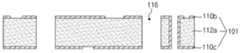
Translated fromKorean도 1은 본 발명의 실시 예에 따른 칩 내장형 인쇄회로기판을 나타내는 도면이다.1 is a view showing a chip embedded printed circuit board according to an embodiment of the invention.
도 2a 내지 도 2g는 도 1에 도시된 본 발명의 실시 예에 따른 칩 내장형 인쇄회로기판의 제조방법을 나타내는 공정 단면도이다.2A to 2G are cross-sectional views illustrating a method of manufacturing a chip embedded printed circuit board according to an exemplary embodiment of the present invention illustrated in FIG. 1.
<도면의 주요 부분에 대한 부호의 설명><Explanation of symbols for main parts of the drawings>
100 : 제 1 기판101 : 제 2 기판100: first substrate 101: second substrate
103 : 제 3 기판110a, 110b, 110c, 110d : 회로패턴103:
112, 112a, 112b : 절연층114 : 칩112, 112a, 112b: insulating layer 114: chip
114a : 칩 전극116, 116a : 홀114a:
본 발명은 칩 내장형 인쇄회로기판 및 그 제조방법에 관한 것으로, 특히 공정시간 및 공정비용을 줄이고 신뢰성을 향상시킬 수 있는 칩 내장형 인쇄회로기판 및 그 제조방법에 관한 것이다.The present invention relates to a chip embedded printed circuit board and a method for manufacturing the same, and more particularly, to a chip embedded printed circuit board and a method for manufacturing the same which can reduce process time and process cost and improve reliability.
최근, 휴대 전화나 디지털 AV기기, IC카드 등 고기능화에 따라 전자 부품의 고기능화, 소형화 요구가 급증하고 있다. 이러한 추세에 대응하고자 패키지의 추세가 기존의 기판 하나에 하나의 칩이 내장되는 형태에서 하나의 기판에 여러 개의 칩을 내장하는 패키지가 등장하게 되었다.In recent years, with the high functionalization of mobile phones, digital AV equipment, IC cards, and the like, the demand for high functionalization and miniaturization of electronic components has increased rapidly. In order to cope with such a trend, the package trend is that one chip is embedded in a single substrate and a package in which several chips are embedded in a single substrate has emerged.
이에 따라, 기판 내에 칩을 실장 하는 칩 내장(Chip Embedded)형 인쇄회로기판의 다양한 제조방법이 연구되고 있고, 칩 부품을 실장 하는 지점에 페이스트, 칩 본드, 테이프 등을 이용하여 칩을 고정하는 방법이 일본 특허공개번호 제2003-204167호에 개시되어 있다.Accordingly, various manufacturing methods of chip embedded printed circuit boards in which chips are mounted in a substrate have been studied, and methods of fixing chips using pastes, chip bonds, and tapes at points where chip components are mounted. this is disclosed in Japanese Patent Publication No. 2003-204167 call.
그러나, 일본 특허공개번호 제2003-204167호에 기재된 칩 내장형 인쇄회로기판의 제조방법은 직접소자 또는 수동소자를 삽입하기 위해 Pre-SMT 공정 즉, 테이프, 칩 본드, 페이스트 등을 부착 또는 첨가하는 공정이 필요하므로 많은 공정시간이 소요될 뿐만 아니라 SMT 이전에 이종 재료가 첨가되므로 재료비 및 공정비용이 증가하는 문제가 있다.However, the method for manufacturing a chip embedded printed circuit board described in Japanese Patent Laid-Open No. 2003-204167 is a process of attaching or adding a pre-SMT process, ie, tape, chip bond, paste, or the like, to insert a direct element or a passive element. Since this requires a lot of processing time, as well as heterogeneous materials are added before SMT there is a problem that the material cost and process cost increases.
또한, 종래 기술에 따른 칩 내장형 인쇄회로기판 및 그 제조방법은 이종 재료의 첨가로 인해 기판 내의 신뢰성 저하가 발생하는 문제가 있다.In addition, the chip-embedded printed circuit board and its manufacturing method according to the prior art have a problem that the reliability is lowered in the substrate due to the addition of different materials.
따라서, 본 발명은 공정시간 및 공정비용을 줄이고 신뢰성을 향상시킬 수 있는 칩 내장형 인쇄회로기판 및 그 제조방법을 제공하는 것을 목적으로 한다.Accordingly, an object of the present invention is to provide a chip-embedded printed circuit board and a method of manufacturing the same which can reduce process time and process cost and improve reliability.
상기 목적을 달성하기 위하여, 본 발명의 실시 예에 따른 칩 내장형 인쇄회로기판은 양면에 전극이 형성된 칩; 제 1 절연층과 상기 제 1 절연층의 하부에 형성된 하부 외층 회로패턴을 포함하고, 상기 제 1 절연층에 상기 칩의 일부가 실장 되며, 상기 하부 외층 회로패턴이 상기 칩의 전극에 연결된 제 1 기판; 제 2 절연층과 상기 제 2 절연층의 양면에 내층 회로패턴이 형성되고, 상기 내층 회로패턴 중 하부 내층 회로패턴이 비아홀을 통해 상기 하부 외층 회로패턴과 전기적으로 연결되며, 상기 제 1 기판에 실장 되지 않은 칩의 나머지 부분이 실장 되는 홀이 형성되어 상기 제 1 기판 위에 적층 된 제 2 기판; 및 제 3 절연층과 상기 제 3 절연층의 상부에 형성된 상부 외층 회로패턴을 포함하고, 상기 상부 외층 회로패턴이 상기 내층 회로패턴 중 상부 내층 회로패턴과 비아홀을 통해 전기적으로 연결되어 상기 제 2 기판 위에 적층 된 제 3 기판을 포함하는 것을 특징으로 한다.In order to achieve the above object, a chip embedded printed circuit board according to an embodiment of the present invention is a chip having an electrode formed on both sides; A first insulating layer and a lower outer circuit pattern formed under the first insulating layer, wherein a portion of the chip is mounted on the first insulating layer and the lower outer circuit pattern is connected to an electrode of the chip; Board; Inner circuit patterns are formed on both surfaces of the second insulation layer and the second insulation layer, and lower inner circuit patterns of the inner circuit patterns are electrically connected to the lower outer circuit patterns through via holes, and are mounted on the first substrate. A second substrate having a hole in which the remaining portion of the chip not mounted is formed and stacked on the first substrate; And an upper outer circuit pattern formed on the third insulating layer and the third insulating layer, wherein the upper outer circuit pattern is electrically connected to an upper inner circuit pattern of the inner circuit pattern through a via hole to form the second substrate. It characterized in that it comprises a third substrate stacked on top.
본 발명의 실시 예에 따른 칩 내장형 인쇄회로기판의 제조방법은 (a) 제 1 절연층과 상기 제 1 절연층의 한 면에 동박이 부착된 제 1 기판을 준비하는 단계; (b) 상기 제 1 절연층을 열처리하여 용융시켜 전극이 양측에 부착된 칩을 상기 제 1 절연층에 부분 실장 하는 단계; (c) 제 2 절연층의 양면에 내층 회로패턴이 형성되고, 상기 칩이 실장 되는 홀이 형성된 제 2 기판을 준비하는 단계; (d) 상기 제 2 기판의 홀에 상기 부분 실장 되지 않은 나머지 부분을 실장하고 제 3 절연층과 동박으로 이루어진 제 3 기판을 상기 제 2 기판의 위에 올린 후 상기 제 1 기판, 제 2 기판 및 제 3 기판을 순차적으로 적층 하는 단계; (e) 상기 제 1 기판 및 제 3 기판에 부착된 외층 동박을 제거하는 단계; 및 (f) 상기 제 1 기판의 하부 및 제 3 기판의 상부에 외층 회로패턴을 형성하는 단계를 포함하는 것을 특징으로 한다.In accordance with another aspect of the present invention, a method of manufacturing a chip embedded printed circuit board may include: (a) preparing a first insulating layer and a first substrate having copper foil attached to one surface of the first insulating layer; (b) heat-treating and melting the first insulating layer to partially mount a chip having electrodes attached to both sides thereof on the first insulating layer; (c) preparing a second substrate having inner circuit patterns formed on both surfaces of a second insulating layer and having holes for mounting the chips; (d) the first substrate, the second substrate, and the first substrate after mounting the remaining portion not partially mounted in the hole of the second substrate and placing a third substrate made of a third insulating layer and copper foil on the second substrate; Stacking three substrates sequentially; (E) removing the outer layer copper foil attached to the first substrate and the third substrate; And (f) forming an outer circuit pattern on the lower portion of the first substrate and the upper portion of the third substrate.
이하, 첨부된 도면을 참조하여 본 발명의 바람직한 실시 예를 상세하게 설명한다.Hereinafter, exemplary embodiments of the present invention will be described in detail with reference to the accompanying drawings.
도 1은 본 발명의 실시 예에 따른 칩 내장형 인쇄회로기판을 나타내는 도면이다.1 is a view showing a chip embedded printed circuit board according to an embodiment of the invention.
도 1을 참조하면, 본 발명의 실시 예에 따른 칩 내장형 인쇄회로기판은 칩(114), 제 1 기판(100), 제 2 기판(101) 및 제 3 기판(102)을 포함한다.Referring to FIG. 1, a chip embedded printed circuit board according to an exemplary embodiment of the present invention includes a
칩(114)은 그 양면에 칩 전극(114a)이 형성되어 있고, 칩 전극(114a)을 통해 제 1 기판(100)의 하부에 형성된 하부 외층 회로패턴(110a)과 전기적으로 연결된다.The
제 1 기판(100)은 제 1 절연층(112)과 하부 외층 회로패턴(110a)으로 이루어지고, 제 1 절연층(112)에 칩(114)의 일부가 실장 되며, 하부 외층 회로패턴(110a)이 칩 전극(114a)과 연결된다.The
제 2 기판(101)은 제 2 절연층(112a)과 그 양면에 형성된 내층 회로패턴(110b, 110c)을 포함하고, 제 1 절연층(112)에 실장 되지 않은 칩(114)의 나머지 부분이 실장 될 홀이 형성된다. 이때, 홀은 제 2 기판(101)을 관통하는 관통홀이거나 하부 내층 회로패턴(110c)과 제 2 절연층(112a)의 일부만을 관통하여 상부에 관통되지 않은 제 2 절연층(112a)이 존재하는 홈 형태로 형성된다.The
또한, 홀은 칩 전극(114a)을 포함하는 칩(114)의 너비와 동일한 너비로 형성되거나 칩(114)의 너비보다 큰 너비를 갖도록 형성된다. 그리고, 홀이 홈 형태로 형성될 경우 홈은 칩(114)의 높이와 동일하게 형성되거나 칩(114)의 높이보다 높게 형성된다.Further, the hole is formed to have the same width as the width of the
제 3 기판(102)은 제 3 절연층(112b)과 상부 외층 회로패턴(110d)으로 이루어져 제 2 기판(101)의 상부에 적층 된다.The
도 2a 내지 도 2g는 본 발명의 실시 예에 따른 칩 내장형 인쇄회로기판의 제조방법을 나타내는 공정 단면도이다.2A to 2G are cross-sectional views illustrating a method of manufacturing a chip embedded printed circuit board according to an exemplary embodiment of the present invention.
먼저, 도 2a에 도시된 바와 같이 제 1 절연층(112)과 제 1 절연층(112)의 한 면에 적층 된 동박(110a)으로 이루어진 제 1 기판(100)을 준비한다. 이때, 제 1 절연층(112)은 열경화성 수지나 열가소성 수지가 사용된다.First, as illustrated in FIG. 2A, a
이후, 제 1 기판(100)에 열처리를 하거나 제 1 기판(100)의 하단부를 가열하여 제 1 절연층(112)을 용융시킨 후 도 2b에 도시된 바와 같이 제 1 절연층(112)에 칩(114)을 실장 한다. 이때, 제 1 절연층(112)의 두께가 칩(114)의 높이보다 낮을 경우 칩(114)은 그 일부가 제 1 절연층(112)에 실장 된다.Thereafter, the
이후, 도 2c에 도시된 바와 같이 양면에 내층 회로패턴(110b, 110c)이 형성되고, 칩(114)이 실장 될 홀이 형성된 제 2 기판(101)을 준비한다. 여기서, 제 2 기판(101)은 코어기판으로 사용된다.Thereafter, as shown in FIG. 2C,
이때, 제 2 기판(101)의 제조방법은 다음과 같다.At this time, the manufacturing method of the
먼저, 제 2 절연층(112a) 및 제 2 절연층(112a)의 양면에 동박(110b, 110c)이 적층 된 동박적층판을 준비한다.First, a copper foil laminated plate in which
이때, 동박적층판의 제 2 절연층(112a)은 기초 재료로 수지가 사용되고, 전 기적인 특성은 뛰어나지만 기계적 강도가 불충분하고 온도에 의한 치수 변화(열팽창률)가 금속의 10배 정도로 큰 수지의 결점을 보완하기 위해 종이, 유리섬유 및 유지부직포 등이 보강기재가 혼합된다.At this time, the
또한, 동박(110b, 110c)은 통상 전해 동박이 사용되고, 수지와의 접착력을 높이기 위해 동박 형성 시 동박이 수지와 화학적으로 반응하여 수지 쪽으로 소정 깊이로 파고들도록 만들어진다.In addition, the
이러한, 동박적층판은 유리/에폭시 동박적층판, 내열수지 동박적층판, 종이/페놀 동박적층판, 고주파용 동박적층판 및 플렉시블 동박적층판 등 여러 가지가 있으나 일반적으로 유리/에폭시 동박적층판이 사용된다.Such copper clad laminates include glass / epoxy copper clad laminates, heat-resistant resin copper clad laminates, paper / phenol copper clad laminates, high frequency copper clad laminates and flexible copper clad laminates, but glass / epoxy copper clad laminates are generally used.
이후, CNC 드릴(Computer Numerical Control Drill) 또는 레이저 드릴을 이용하여 칩 또는 부품이 실장 될 영역에 홀을 형성한다.Then, holes are formed in the area where the chip or component is to be mounted by using a CNC drill (Computer Numerical Control Drill) or a laser drill.
여기서, CNC 드릴을 이용하는 방식은 양면 인쇄회로기판의 비아홀이나 다층 인쇄회로기판의 도통홀을 형성할 때 적당하고, 레이저를 이용하는 방식은 다층 인쇄회로기판의 마이크로 비아홀을 형성할 때 적당하다.Here, the method using the CNC drill is suitable for forming the via hole of the double-sided printed circuit board or the through hole of the multilayer printed circuit board, and the method using the laser is suitable for forming the micro via hole of the multilayer printed circuit board.
이때, 레이저를 이용할 경우 YAG 레이저(Yttrium Aluminum Garnet Laser)를이용하여 동박과 절연층을 동시에 가공할 수 있고, 비아홀이 형성될 부분의 동박을 식각한 후 이산화탄소 레이저(CO2 Laser)를 이용하여 절연층을 가공할 수 있다.At this time, in case of using laser, YAG laser (Yttrium Aluminum Garnet Laser) can be used to process copper foil and insulating layer at the same time, and after etching copper foil of the part where via hole is to be formed, it is insulated using CO2 laser. The layer can be processed.
홀은 도 2c에 도시된 바와 같이 동박적층판을 관통하는 관통홀(116)로 형성되거나 칩(114)의 높이 만큼 하부 동박(110c)과 제 2 절연층(112a)의 일부가 파인 홈으로 형성될 수 있다.The hole may be formed as a through
이러한, 홀은 홀 내부에 실장 되는 칩 또는 부품보다 큰 너비를 갖도록 형성되거나 칩 또는 부품의 너비와 동일하게 형성된다. 또한, 홀이 홈 형태로 형성될 경우 홈 내부에 칩이 완전하게 실장 될 수 있도록 홈은 칩 또는 부품의 높이와 동일하거나 더 큰 높이를 갖도록 형성된다.Such a hole may be formed to have a larger width than the chip or component mounted inside the hole, or may be formed to have the same width as the chip or component. In addition, when the hole is formed in the groove shape, the groove is formed to have a height equal to or greater than the height of the chip or component so that the chip can be completely mounted inside the groove.
홀을 형성한 후에는 디버링(Deburring) 및 디스미어(Desmear) 공정으로 홀 형성 시 발생하는 각종 오염과 이물질을 제거한다.After forming the holes, deburring and desmear processes remove various contaminants and foreign substances generated during hole formation.
여기서, 디버링 공정은 드릴링 가공 시 발생 되는 동박의 버(burr) 및 홀 내벽의 먼지 입자와 동박 표면의 먼지, 지문 등을 제거하는 공정이고, 디스미어 공정은 드릴링 가공 시 홀 내벽에 부착되는 스미어(smear)를 제거하기 위한 공정이다.Here, the deburring process is to remove the burr of the copper foil and dust particles on the inner wall of the hole and dust, fingerprints, etc. on the surface of the copper foil generated during the drilling process, the desmear process is a smear attached to the inner wall of the hole during the drilling process ( process to remove smear).
이후, 화상 형성 공정을 통해 내층 회로패턴(110b, 110c)을 형성한다. 이때, 내층 회로패턴(110b, 110c)은 사진 식각 공정이나 스크린 인쇄 공정을 통해 형성된다.Thereafter, the
여기서, 사진 식각 공정은 아트워크 필름에 인쇄된 회로패턴을 기판상에 전사하는 방식으로 전사 방법에는 여러 가지 방법이 있으나, 가장 흔히 사용되는 방법으로는 감광성의 드라이 필름을 사용하여 자외선에 의해 아트워크 필름에 인쇄된 회로패턴을 드라이 필름으로 전사하는 방식이다.Here, the photolithography process is a method of transferring the circuit pattern printed on the artwork film on the substrate, there are a number of methods of the transfer method, the most commonly used method using a photosensitive dry film by ultraviolet rays artwork The circuit pattern printed on the film is transferred to a dry film.
또한, 스크린 인쇄 공정은 스크린 판을 이용하여 배선패턴을 전사하는 방법으로 회로패턴을 형성하는 방법이다.In addition, the screen printing process is a method of forming a circuit pattern by the method of transferring a wiring pattern using a screen plate.
제 2 기판(101)이 완성된 후에는 프레스로 가열, 가압하여 제 1 기판(100), 제 2 기판(101) 및 제 3 절연층(112b)과 동박(110d)으로 이루어진 제 3 기판(102)을 도 2d에 도시된 바와 같이 순차적으로 적층 시킨다.After the
이때, 제 1 기판(100)에 일부 실장 된 칩(114)은 나머지 부분에 제 2 기판(101)에 형성된 홀에 실장 된다. 그리고, 제 2 기판(101)에 형성된 홀이 칩(114)의 너비와 동일한 크기로 형성되어 있는 경우에는 칩(114)의 상부에만 제 3 절연층(112b)이 적층 되나 제 2 기판(101)에 형성된 홀이 칩(114)의 너비보다 크게 형성되어 있는 경우에는 칩 전극(114a)과 제 2 절연층(112a) 사이에 제 3 절연층(112b)이 적층 된다.At this time, the
이후, 에칭액을 이용하여 도 2e에 도시된 바와 같이 제 1 기판(100) 및 제 3 기판(102)에 적층 된 외층 동박(110a, 110d)을 제거한다.Thereafter, as illustrated in FIG. 2E, the outer layer copper foils 110a and 110d stacked on the
외층 동박(110a, 110d)을 제거한 후에는 디스미어 공정으로 칩 전극(114a)의 하부에 남아있는 수지를 제거한다.After the outer layer copper foils 110a and 110d are removed, the resin remaining in the lower portion of the
이후, 무전해 동도금 과정을 통해 도 2f에 도시된 바와 같이 제 1 기판(100)의 하부와 제 3 기판(102)의 상부에 동도금층(110a, 110d)을 형성한다.Thereafter, as shown in FIG. 2F,
동도금층(110a, 110d)을 형성한 후에는 레이저를 이용하여 비아홀(116a)을 형성한 후 동도금층(110a, 110d) 위에 드라이 필름을 부착하여 노광 및 현상 처리한다. 이후, 전해 동도금 공정을 통해 드라이 필름이 부착되지 않은 회로패턴 형성부분에 동도금층을 형성한 후 드라이 필름을 제거한다. 드라이 필름이 제거된 후에는 플래쉬 에칭을 통해 드라이 필름이 부착되었던 부분의 동도금층을 제거하여 도 2g와 같은 외층 회로패턴(110a, 110d)을 형성한다.After the
그러나, 도 2f에서 무전해 동도금 후 전해 동도금을 통해 동도금층(110a, 110d)을 형성할 경우에는 무전해 동도금 및 전해 동도금 공정을 통해 동도금층(110a, 110d)을 형성한 뒤 도 2g에 도시된 바와 같이 레이저를 이용하여 비아홀(116a)을 형성한다. 비아홀(116a)이 형성되면, 동도금층(110a, 100d) 위에 드라이 필름을 부착한 후 노광 및 현상을 통해 회로패턴이 형성되지 않는 부분의 드라이 필름을 제거한 후 에칭액으로 동도금층(110a, 110d)을 에칭하여 회로패턴을 형성한다. 이후, 회로패턴 위에 부착된 드라이 필름을 제거하여 도 2g와 같은 외층 회로패턴(110a, 110d)이 형성한다.However, in the case of forming the
외층 회로패턴(110a, 110d)을 형성한 후에는 통상의 인쇄회로기판 공정에 따라 솔더 레지스트를 도포하고, 노광, 현상 및 건조 공정을 거쳐 전원의 공급 및 신호의 교환을 위해 외부 단자와 연결되는 부분 즉, 와이어 본딩 패드 및 솔더볼 패드로 사용되는 부분을 제외한 나머지 영역에 솔더 레지스트 패턴을 형성한 후 금, 니켈, 로듐 등과 같이 경도가 높고 도전성이 좋은 금속으로 도전층을 형성한다.After the
이와 같이 본 발명의 실시 예에 따른 칩 내장형 인쇄회로기판 및 그 제조방법은 열처리 이외에 추가적인 재료를 기판 내에 삽입하지 않았기 때문에 Pre-SMT 공정에서 발생 되는 페이스트, 칩 본드 및 테이프 등의 공정비용 및 재료비용을 줄일 수 있게 된다.As described above, the chip embedded printed circuit board and the method of manufacturing the same according to an embodiment of the present invention do not insert additional materials into the substrate except for heat treatment, and thus, process and material costs such as paste, chip bond, and tape generated in the pre-SMT process. Can be reduced.
또한, 본 발명의 실시 예에 따른 칩 내장형 인쇄회로기판 및 그 제조방법은 기판 내에 이종 재료가 첨가되지 않기 때문에 신뢰성 저하를 방지할 수 있게 된다.In addition, the chip embedded printed circuit board and the method of manufacturing the same according to an exemplary embodiment of the present invention can prevent deterioration of reliability because no heterogeneous material is added to the substrate.
상술한 바와 같이, 본 발명은 열처리 이외에 추가적인 재료를 기판 내에 삽입하지 않았기 때문에 Pre-SMT 공정에서 발생 되는 페이스트, 칩 본드 및 테이프 등의 공정비용 및 재료비용을 줄일 수 있고, 기판 내에 이종 재료가 첨가되지 않기 때문에 신뢰성 저하를 방지할 수 있다.As described above, since the present invention does not insert additional materials into the substrate other than the heat treatment, it is possible to reduce the processing costs and material costs of pastes, chip bonds, and tapes generated in the pre-SMT process, and to add heterogeneous materials to the substrate. It can not prevent reliability degradation because.
여기서, 상술한 본 발명에서는 바람직한 실시예를 참조하여 설명하였지만, 해당 기술분야의 숙련된 당업자는 하기의 특허청구범위에 기재된 본 발명의 사상 및 영역으로부터 벗어나지 않는 범위 내에서 본 발명을 다양하게 수정 및 변경할 수 있음을 이해할 수 있을 것이다.Herein, the present invention described above has been described with reference to preferred embodiments, but those skilled in the art can variously modify the present invention without departing from the spirit and scope of the present invention as set forth in the claims below. It will be appreciated that this can be changed.
Claims (9)
Translated fromKoreanPriority Applications (1)
| Application Number | Priority Date | Filing Date | Title |
|---|---|---|---|
| KR1020060048180AKR100771320B1 (en) | 2006-05-29 | 2006-05-29 | Chip embedded printed circuit board and its manufacturing method |
Applications Claiming Priority (1)
| Application Number | Priority Date | Filing Date | Title |
|---|---|---|---|
| KR1020060048180AKR100771320B1 (en) | 2006-05-29 | 2006-05-29 | Chip embedded printed circuit board and its manufacturing method |
Publications (1)
| Publication Number | Publication Date |
|---|---|
| KR100771320B1true KR100771320B1 (en) | 2007-10-29 |
Family
ID=38816255
Family Applications (1)
| Application Number | Title | Priority Date | Filing Date |
|---|---|---|---|
| KR1020060048180AExpired - Fee RelatedKR100771320B1 (en) | 2006-05-29 | 2006-05-29 | Chip embedded printed circuit board and its manufacturing method |
Country Status (1)
| Country | Link |
|---|---|
| KR (1) | KR100771320B1 (en) |
Cited By (3)
| Publication number | Priority date | Publication date | Assignee | Title |
|---|---|---|---|---|
| CN102136431A (en)* | 2010-01-22 | 2011-07-27 | 亿光电子工业股份有限公司 | Light emitting diode package and manufacturing method thereof |
| KR101187977B1 (en) | 2009-12-08 | 2012-10-05 | 삼성전기주식회사 | Package substrate and fabricating method of the same |
| US20240364065A1 (en)* | 2023-04-28 | 2024-10-31 | Logitech Europe S.A. | Techniques for soldering on a substrate with a below soldering temperature melting point |
Citations (4)
| Publication number | Priority date | Publication date | Assignee | Title |
|---|---|---|---|---|
| JP2002204071A (en)* | 2000-01-31 | 2002-07-19 | Ngk Spark Plug Co Ltd | Method of manufacturing wiring board |
| JP2003142806A (en)* | 2001-11-07 | 2003-05-16 | Alps Electric Co Ltd | Mounting method for chip component |
| JP2005191156A (en)* | 2003-12-25 | 2005-07-14 | Mitsubishi Electric Corp | Electrical component built-in wiring board and method for manufacturing the same |
| KR20060005840A (en) | 2004-07-14 | 2006-01-18 | 삼성전기주식회사 | Manufacturing Method of Printed Circuit Board with Passive Device Chip |
- 2006
- 2006-05-29KRKR1020060048180Apatent/KR100771320B1/ennot_activeExpired - Fee Related
Patent Citations (4)
| Publication number | Priority date | Publication date | Assignee | Title |
|---|---|---|---|---|
| JP2002204071A (en)* | 2000-01-31 | 2002-07-19 | Ngk Spark Plug Co Ltd | Method of manufacturing wiring board |
| JP2003142806A (en)* | 2001-11-07 | 2003-05-16 | Alps Electric Co Ltd | Mounting method for chip component |
| JP2005191156A (en)* | 2003-12-25 | 2005-07-14 | Mitsubishi Electric Corp | Electrical component built-in wiring board and method for manufacturing the same |
| KR20060005840A (en) | 2004-07-14 | 2006-01-18 | 삼성전기주식회사 | Manufacturing Method of Printed Circuit Board with Passive Device Chip |
Cited By (4)
| Publication number | Priority date | Publication date | Assignee | Title |
|---|---|---|---|---|
| KR101187977B1 (en) | 2009-12-08 | 2012-10-05 | 삼성전기주식회사 | Package substrate and fabricating method of the same |
| CN102136431A (en)* | 2010-01-22 | 2011-07-27 | 亿光电子工业股份有限公司 | Light emitting diode package and manufacturing method thereof |
| CN102136431B (en)* | 2010-01-22 | 2013-07-24 | 亿光电子工业股份有限公司 | Light emitting diode package and manufacturing method thereof |
| US20240364065A1 (en)* | 2023-04-28 | 2024-10-31 | Logitech Europe S.A. | Techniques for soldering on a substrate with a below soldering temperature melting point |
Similar Documents
| Publication | Publication Date | Title |
|---|---|---|
| KR100965339B1 (en) | Electronic component embedded printed circuit board and manufacturing method | |
| US7282394B2 (en) | Printed circuit board including embedded chips and method of fabricating the same using plating | |
| US7506437B2 (en) | Printed circuit board having chip package mounted thereon and method of fabricating same | |
| US8687380B2 (en) | Wiring board and method for manufacturing the same | |
| US7485569B2 (en) | Printed circuit board including embedded chips and method of fabricating the same | |
| KR100733253B1 (en) | High density printed circuit board and manufacturing method thereof | |
| US20080296056A1 (en) | Printed circuit board, production method therefor, electronic-component carrier board using printed circuit board, and production method therefor | |
| US20120030938A1 (en) | Method of manufacturing printed circuit board | |
| JPWO2007126090A1 (en) | CIRCUIT BOARD, ELECTRONIC DEVICE DEVICE, AND CIRCUIT BOARD MANUFACTURING METHOD | |
| US20120017435A1 (en) | Method of manufacturing PCB having electronic components embedded therein | |
| JP2008124247A (en) | Component built-in substrate and manufacturing method thereof | |
| KR20160059125A (en) | Element embedded printed circuit board and method of manufacturing the same | |
| JP4129166B2 (en) | Electrolytic copper foil, film with electrolytic copper foil, multilayer wiring board, and manufacturing method thereof | |
| KR100771320B1 (en) | Chip embedded printed circuit board and its manufacturing method | |
| KR100752017B1 (en) | Manufacturing method of printed circuit board | |
| KR100905642B1 (en) | Chip embedded printed circuit board and its manufacturing method | |
| KR101109287B1 (en) | Electronic component embedded printed circuit board and manufacturing method | |
| KR100651423B1 (en) | Method for manufacturing a multi-layer printed circuit board | |
| KR100771319B1 (en) | Chip embedded printed circuit board and its manufacturing method | |
| KR100648971B1 (en) | Manufacturing method of embedded printed circuit board | |
| KR100699237B1 (en) | Embedded printed circuit board manufacturing method | |
| KR100797669B1 (en) | Printed Circuit Board and Manufacturing Method | |
| KR100797693B1 (en) | Manufacturing method of chip embedded printed circuit board | |
| JP2006049457A (en) | Wiring board with built-in parts and manufacturing method thereof | |
| KR20060132182A (en) | Manufacturing method of printed circuit board for laminated package |
Legal Events
| Date | Code | Title | Description |
|---|---|---|---|
| A201 | Request for examination | ||
| PA0109 | Patent application | St.27 status event code:A-0-1-A10-A12-nap-PA0109 | |
| PA0201 | Request for examination | St.27 status event code:A-1-2-D10-D11-exm-PA0201 | |
| R18-X000 | Changes to party contact information recorded | St.27 status event code:A-3-3-R10-R18-oth-X000 | |
| D13-X000 | Search requested | St.27 status event code:A-1-2-D10-D13-srh-X000 | |
| D14-X000 | Search report completed | St.27 status event code:A-1-2-D10-D14-srh-X000 | |
| E902 | Notification of reason for refusal | ||
| PE0902 | Notice of grounds for rejection | St.27 status event code:A-1-2-D10-D21-exm-PE0902 | |
| P11-X000 | Amendment of application requested | St.27 status event code:A-2-2-P10-P11-nap-X000 | |
| P13-X000 | Application amended | St.27 status event code:A-2-2-P10-P13-nap-X000 | |
| E701 | Decision to grant or registration of patent right | ||
| PE0701 | Decision of registration | St.27 status event code:A-1-2-D10-D22-exm-PE0701 | |
| GRNT | Written decision to grant | ||
| PR0701 | Registration of establishment | St.27 status event code:A-2-4-F10-F11-exm-PR0701 | |
| PR1002 | Payment of registration fee | St.27 status event code:A-2-2-U10-U11-oth-PR1002 Fee payment year number:1 | |
| PG1601 | Publication of registration | St.27 status event code:A-4-4-Q10-Q13-nap-PG1601 | |
| G170 | Re-publication after modification of scope of protection [patent] | ||
| PG1701 | Publication of correction | St.27 status event code:A-5-5-P10-P19-oth-PG1701 Patent document republication publication date:20080416 Republication note text:Request for Correction Notice (Document Request) Gazette number:1007713200000 Gazette reference publication date:20071029 | |
| PR1001 | Payment of annual fee | St.27 status event code:A-4-4-U10-U11-oth-PR1001 Fee payment year number:4 | |
| PR1001 | Payment of annual fee | St.27 status event code:A-4-4-U10-U11-oth-PR1001 Fee payment year number:5 | |
| FPAY | Annual fee payment | Payment date:20121002 Year of fee payment:6 | |
| PR1001 | Payment of annual fee | St.27 status event code:A-4-4-U10-U11-oth-PR1001 Fee payment year number:6 | |
| FPAY | Annual fee payment | Payment date:20130916 Year of fee payment:7 | |
| PR1001 | Payment of annual fee | St.27 status event code:A-4-4-U10-U11-oth-PR1001 Fee payment year number:7 | |
| R18-X000 | Changes to party contact information recorded | St.27 status event code:A-5-5-R10-R18-oth-X000 | |
| LAPS | Lapse due to unpaid annual fee | ||
| PC1903 | Unpaid annual fee | St.27 status event code:A-4-4-U10-U13-oth-PC1903 Not in force date:20141024 Payment event data comment text:Termination Category : DEFAULT_OF_REGISTRATION_FEE | |
| PC1903 | Unpaid annual fee | St.27 status event code:N-4-6-H10-H13-oth-PC1903 Ip right cessation event data comment text:Termination Category : DEFAULT_OF_REGISTRATION_FEE Not in force date:20141024 | |
| P22-X000 | Classification modified | St.27 status event code:A-4-4-P10-P22-nap-X000 | |
| P22-X000 | Classification modified | St.27 status event code:A-4-4-P10-P22-nap-X000 | |
| R18-X000 | Changes to party contact information recorded | St.27 status event code:A-5-5-R10-R18-oth-X000 |