KR100770827B1 - Key pad and keypad assembly - Google Patents
Key pad and keypad assemblyDownload PDFInfo
- Publication number
- KR100770827B1 KR100770827B1KR1020050064348AKR20050064348AKR100770827B1KR 100770827 B1KR100770827 B1KR 100770827B1KR 1020050064348 AKR1020050064348 AKR 1020050064348AKR 20050064348 AKR20050064348 AKR 20050064348AKR 100770827 B1KR100770827 B1KR 100770827B1
- Authority
- KR
- South Korea
- Prior art keywords
- guide plate
- light guide
- light
- keypad
- key button
- Prior art date
- Legal status (The legal status is an assumption and is not a legal conclusion. Google has not performed a legal analysis and makes no representation as to the accuracy of the status listed.)
- Expired - Fee Related
Links
Images


Classifications
- H—ELECTRICITY
- H01—ELECTRIC ELEMENTS
- H01H—ELECTRIC SWITCHES; RELAYS; SELECTORS; EMERGENCY PROTECTIVE DEVICES
- H01H13/00—Switches having rectilinearly-movable operating part or parts adapted for pushing or pulling in one direction only, e.g. push-button switch
- H01H13/70—Switches having rectilinearly-movable operating part or parts adapted for pushing or pulling in one direction only, e.g. push-button switch having a plurality of operating members associated with different sets of contacts, e.g. keyboard
- H01H13/83—Switches having rectilinearly-movable operating part or parts adapted for pushing or pulling in one direction only, e.g. push-button switch having a plurality of operating members associated with different sets of contacts, e.g. keyboard characterised by legends, e.g. Braille, liquid crystal displays, light emitting or optical elements
- H—ELECTRICITY
- H01—ELECTRIC ELEMENTS
- H01H—ELECTRIC SWITCHES; RELAYS; SELECTORS; EMERGENCY PROTECTIVE DEVICES
- H01H13/00—Switches having rectilinearly-movable operating part or parts adapted for pushing or pulling in one direction only, e.g. push-button switch
- H01H13/70—Switches having rectilinearly-movable operating part or parts adapted for pushing or pulling in one direction only, e.g. push-button switch having a plurality of operating members associated with different sets of contacts, e.g. keyboard
- H01H13/702—Switches having rectilinearly-movable operating part or parts adapted for pushing or pulling in one direction only, e.g. push-button switch having a plurality of operating members associated with different sets of contacts, e.g. keyboard with contacts carried by or formed from layers in a multilayer structure, e.g. membrane switches
- H01H13/704—Switches having rectilinearly-movable operating part or parts adapted for pushing or pulling in one direction only, e.g. push-button switch having a plurality of operating members associated with different sets of contacts, e.g. keyboard with contacts carried by or formed from layers in a multilayer structure, e.g. membrane switches characterised by the layers, e.g. by their material or structure
- H—ELECTRICITY
- H01—ELECTRIC ELEMENTS
- H01H—ELECTRIC SWITCHES; RELAYS; SELECTORS; EMERGENCY PROTECTIVE DEVICES
- H01H2219/00—Legends
- H01H2219/036—Light emitting elements
- H01H2219/044—Edge lighting of layer
- H—ELECTRICITY
- H01—ELECTRIC ELEMENTS
- H01H—ELECTRIC SWITCHES; RELAYS; SELECTORS; EMERGENCY PROTECTIVE DEVICES
- H01H2219/00—Legends
- H01H2219/054—Optical elements
- H01H2219/056—Diffuser; Uneven surface
- H—ELECTRICITY
- H01—ELECTRIC ELEMENTS
- H01H—ELECTRIC SWITCHES; RELAYS; SELECTORS; EMERGENCY PROTECTIVE DEVICES
- H01H2219/00—Legends
- H01H2219/054—Optical elements
- H01H2219/06—Reflector
- H—ELECTRICITY
- H01—ELECTRIC ELEMENTS
- H01H—ELECTRIC SWITCHES; RELAYS; SELECTORS; EMERGENCY PROTECTIVE DEVICES
- H01H2219/00—Legends
- H01H2219/054—Optical elements
- H01H2219/062—Light conductor
Landscapes
- Push-Button Switches (AREA)
Abstract
Translated fromKoreanDescription
Translated fromKorean도 1은 종래에 따른 키 패드 어셈블리를 나타내는 단면도,1 is a cross-sectional view showing a keypad assembly according to the prior art,
도 2는 본 발명의 바람직한 제1 실시예에 따른 키 패드 어셈블리를 나타내는 단면도,2 is a cross-sectional view showing a keypad assembly according to a first embodiment of the present invention;
도 3은 도 2에 도시된 키패드 어셈블리의 일부분을 개략적으로 나타낸 평면도,3 is a plan view schematically showing a part of the keypad assembly shown in FIG. 2;
도 4는 본 발명의 바람직한 제2 실시예에 따른 키 패드 어셈블리를 나타내는 단면도,4 is a cross-sectional view showing a keypad assembly according to a second preferred embodiment of the present invention;
도 5는 본 발명의 바람직한 제3 실시예에 따른 키 패드 어셈블리의 일부분을 개략적으로 나타내는 평면도,5 is a plan view schematically showing a part of a keypad assembly according to a third preferred embodiment of the present invention;
도 6은 본 발명의 제3 실시예에 대한 비교예를 나타내는 평면도.6 is a plan view showing a comparative example to the third embodiment of the present invention.
본 발명은 휴대용 단말기 등에 구비되는 키 패드(keypad)에 관한 것으로서, 도광판(light guide panel)을 갖는 키 패드 및 키 패드 어셈블리(keypad assembly) 에 관한 것이다.BACKGROUND OF THE INVENTION 1. Field of the Invention The present invention relates to a keypad provided in a portable terminal and the like, and more particularly, to a keypad and a keypad assembly having a light guide panel.
종래의 휴대용 단말기에 사용되는 키 패드는 판 형상을 갖는 탄성 패드(elastic pad)와, 상기 탄성 패드의 상면 상에 형성되며 각각 그 상면에 문자 등이 인쇄된 복수의 키 버튼(key button)과, 상기 상면의 반대편에 위치하는 상기 탄성 패드의 하면 상에 형성된 복수의 돌기(protrusion)(또는 엑츄에이터(actuator))를 포함한다. 또한, 상기 휴대용 단말기는 상기 키 패드를 백라이팅(backlighting)하기 위한 복수의(통상적으로 15~20개 정도) 발광 소자들(light emitting device)을 갖는 것이 통상적이다.Key pads used in conventional portable terminals include an elastic pad having a plate shape, a plurality of key buttons formed on an upper surface of the elastic pad, each of which has letters printed on the upper surface thereof; It includes a plurality of protrusions (or actuators) formed on the lower surface of the elastic pad located opposite the upper surface. In addition, the portable terminal typically has a plurality of light emitting devices (typically about 15 to 20) for backlighting the keypad.
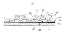
도 1은 종래에 따른 키 패드 어셈블리를 나타내는 단면도이다. 상기 키 패드 어셈블리(100)는 키 패드(110)와, 스위치 기판(switch board, 150)과, 복수의 발광 다이오드(light emitting diode: LED, 170)를 포함한다.1 is a cross-sectional view showing a keypad assembly according to the prior art. The
상기 키 패드(110)는 판 형상을 갖는 탄성 패드(120)와, 상기 탄성 패드(120)의 상면(122) 상에 형성되며 각각 그 상면에 문자 등이 인쇄된 복수의 키 버튼(140)과, 상기 상면(122)의 반대편에 위치하는 상기 탄성 패드(120)의 하면(124) 상에 형성된 복수의 돌기(130)를 포함한다. 상기 각 키 버튼(140)의 중앙에 해당 돌기(130)가 정렬된다. 상기 탄성 패드(120)의 하면(124) 상에는 복수의 홈들(groove, 126)이 형성된다. 상기 홈들(126)은 상기 각 돌기(130)의 둘레에 배치되며, 상기 발광 다이오드들(170)과 상기 돌기들(130)의 간섭을 피하도록 형성된다.The
상기 스위치 기판(150)은 판 형상의 인쇄회로기판(printed circuit board: PCB, 155)과, 상기 키 패드(110)와 대향하는 상기 인쇄회로기판(155)의 상면 상에 형성된 복수의 스위치들(160)을 구비한다. 상기 각 스위치(160)는 도전성 접촉 부재(contact member, 162)와, 상기 접촉 부재(162)를 완전히 덮는 도전성 돔(dome, 164)으로 구성된다.The
상기 복수의 발광 다이오드(170)는 상기 인쇄회로기판(155)의 상면 상에 탑재되며, 상기 각 발광 다이오드(170)는 상기 탄성 패드(120)의 해당 홈(126)에 의해 덮여지도록 위치한다.The plurality of
사용자가 어느 한 키 버튼(140)을 누르면, 상기 키 버튼(140)의 아래에 위치하는 상기 키 패드(110)의 부분이 상기 스위치 기판(150) 측으로 변형됨에 따라, 상기 변형된 부분에 속하는 해당 돌기(130)가 해당 돔(164)을 누르게 된다. 상기 눌려진 돔(164)은 해당 접촉 부재(162)와 전기적 접촉을 이루게 된다.When the user presses any one
상기 스위치들(160)의 작동을 위해, 상기 각 발광 다이오드(170)는 해당 키 버튼(140)의 아래에 위치될 수 없다. 상기 각 발광 다이오드(170)로부터 출력된 광은 상기 탄성 패드(120)를 지나서 상기 키 버튼(140)을 사각으로 조명하게 되므로, 상기 키 버튼(140)의 조명은 불균일하고 어둡다는 문제점이 있다. 즉, 각 키 버튼(140)의 중심 부분은 조명이 상대적으로 어둡고, 상기 키 버튼(140)의 가장자리 부분은 조명이 상대적으로 밝게 된다. 또한, 상기 키 버튼들(140)을 균일하고 밝게 조명하기 위해서, 더욱 많은 수의 발광 다이오드들을 설치하게 되면, 전력 소비량이 높아지고 제조 비용이 상승하게 된다는 문제점이 있다.For the operation of the
본 발명은 상술한 종래의 문제점을 해결하기 위하여 도출된 것으로서, 본 발명의 목적은 균일하고 높은 밝기, 낮은 전력 소비량 및 저렴한 제조 비용을 구현할 수 있는 키 패드 및 키 패드 어셈블리를 제공함에 있다.SUMMARY OF THE INVENTION The present invention was derived to solve the above-mentioned conventional problems, and an object of the present invention is to provide a keypad and a keypad assembly capable of realizing uniform and high brightness, low power consumption and low manufacturing cost.
상기한 문제점을 해결하기 위하여, 본 발명의 제1 측면에 따른 키 패드는, 그 내부로 광이 진행하는 도광판과; 상기 도광판의 상면 상에 배치된 적어도 하나의 키 버튼을 포함하고, 상기 키 버튼은 상기 광의 전반사 조건을 파괴하는 굴절률을 갖는 접착 부재에 의해 상기 도광판의 상면에 부착된다.In order to solve the above problems, the keypad according to the first aspect of the present invention, the light guide plate through which the light propagates; And at least one key button disposed on an upper surface of the light guide plate, wherein the key button is attached to the upper surface of the light guide plate by an adhesive member having a refractive index that destroys the total reflection condition of the light.
또한, 본 발명의 제2 측면에 따른 키 패드는, 그 내부로 광이 진행하는 투명한 고무 재질의 도광판과; 상기 도광판의 상면 상에 배치된 적어도 하나의 키 버튼과; 상기 도광판 상에 국부적으로 형성되며, 상기 도광판 내로 진행하는 광의 일부를 상기 키 버튼 측으로 반사하는 적어도 하나의 반사 패턴을 포함하고, 상기 키 버튼은 상기 광의 전반사 조건을 파괴하는 굴절률을 갖는 접착 부재에 의해 상기 도광판의 상면에 부착된다.In addition, the keypad according to the second aspect of the present invention, the light guide plate made of a transparent rubber material that light propagates therein; At least one key button disposed on an upper surface of the light guide plate; At least one reflection pattern formed locally on the light guide plate and reflecting a portion of the light traveling into the light guide plate toward the key button, wherein the key button is formed by an adhesive member having a refractive index that destroys the total reflection condition of the light. It is attached to the upper surface of the light guide plate.
또한, 본 발명의 제3 측면에 따른 키 패드 어셈블리는, 그 내부로 광이 진행하는 도광판과, 상기 도광판의 상면 상에 배치된 복수의 키 버튼과, 상기 도광판에 형성되며 상기 도광판 내로 진행하는 광의 일부를 상기 키 버튼들 측으로 반사하는 복수의 반사 패턴을 포함하고, 상기 각 키 버튼은 상기 광의 전반사 조건을 파괴하는 굴절률을 갖는 접착 부재에 의해 상기 도광판의 상면에 부착된 키 패드와; 상기 키 패드와 대면하는 상면 상에 배치된 복수의 스위치를 구비하는 스위치 기판과; 상기 도광판의 측면과 대면하도록 배치되며, 상기 도광판의 내부로 광을 결합시키는 적어도 하나의 발광 소자를 포함하며, 상기 도광판의 상측으로 출사되는 전체적인 광량 분포를 균일하게 조절하기 위해, 상기 발광 소자를 기준으로 하여, 상대적으로 가까운 위치의 반사 패턴의 밀도를 저밀도로 하고, 상대적으로 먼 위치의 반사 패턴의 밀도를 고밀도로 한다.In addition, the keypad assembly according to the third aspect of the present invention, the light guide plate through which light propagates therein, a plurality of key buttons disposed on the upper surface of the light guide plate, the light formed on the light guide plate and proceeds into the light guide plate A plurality of reflection patterns reflecting a part toward the key buttons, wherein each key button is attached to an upper surface of the light guide plate by an adhesive member having a refractive index that destroys the total reflection condition of the light; A switch substrate having a plurality of switches disposed on an upper surface facing the keypad; It is disposed to face the side of the light guide plate, and includes at least one light emitting device for coupling the light into the light guide plate, in order to uniformly control the overall light quantity distribution emitted to the upper side of the light guide plate, the light emitting element is referred to As a result, the density of the reflection pattern at a relatively close position is made low, and the density of the reflection pattern at a relatively far position is made high.
또한, 본 발명의 제4 측면에 따라, 그 내부로 광이 진행하는 도광판과, 상기 도광판의 상면 상에 배치된 복수의 키 버튼과, 상기 도광판에 형성되며 상기 도광판 내로 진행하는 광의 일부를 상기 키 버튼들 측으로 반사하는 복수의 반사 패턴을 포함하고, 상기 각 키 버튼은 상기 광의 전반사 조건을 파괴하는 굴절률을 갖는 접착 부재에 의해 상기 도광판의 상면에 부착된 키 패드와; 상기 키 패드와 대면하는 상면 상에 배치된 복수의 스위치를 구비하는 스위치 기판과; 상기 도광판의 측면과 대면하도록 배치되며, 상기 도광판의 내부로 광을 결합시키는 적어도 하나의 발광 소자와; 상기 발광 소자와 대면하는 상기 도광판의 측면에 구비되며, 상기 발광 소자로부터 입사된 광을 확산하는 확산 부재를 포함한다.According to a fourth aspect of the present invention, there is provided a light guide plate through which light propagates therein, a plurality of key buttons disposed on an upper surface of the light guide plate, and a portion of the light formed on the light guide plate and traveling into the light guide plate. A plurality of reflection patterns reflecting toward the buttons, wherein each key button comprises: a keypad attached to an upper surface of the light guide plate by an adhesive member having a refractive index breaking the total reflection condition of the light; A switch substrate having a plurality of switches disposed on an upper surface facing the keypad; At least one light emitting element disposed to face a side surface of the light guide plate and coupling light into the light guide plate; It is provided on the side of the light guide plate facing the light emitting element, and includes a diffusion member for diffusing light incident from the light emitting element.
이하에서는 첨부 도면들을 참조하여 본 발명의 실시 예를 상세히 설명하기로 한다. 본 발명을 설명함에 있어서, 관련된 공지 기능이나 구성에 대한 구체적인 설명은 본 발명의 요지를 모호하지 않게 하기 위하여 생략한다.Hereinafter, with reference to the accompanying drawings will be described an embodiment of the present invention; In describing the present invention, detailed descriptions of related well-known functions and configurations are omitted in order not to obscure the subject matter of the present invention.
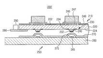
도 2는 본 발명의 바람직한 제1 실시예에 따른 키 패드 어셈블리를 나타내는 단면도이고, 도 3은 상기 키패드 어셈블리의 일부분을 개략적으로 나타낸 평면도이다. 상기 키 패드 어셈블리(200)는 키 패드(210)와, 상기 키 패드(210)와 대향되게(바람직하게는, 상기 키 패드(210)의 돌기들(240)과 맞닿도록) 배치된 스위치 기판(250)과, 적어도 하나의 발광 소자(290)와, 제2 인쇄회로기판(280)을 포함한다.2 is a cross-sectional view showing a keypad assembly according to a first preferred embodiment of the present invention, Figure 3 is a plan view schematically showing a portion of the keypad assembly. The
상기 키 패드(210)는 도광판(220)과, 복수의 키 버튼(245)과, 복수의 돌기(240)와, 복수의 반사 패턴(reflective pattern, 230)(속이 검은색으로 채워진 삼각형으로 표시함)을 포함한다.The
상기 도광판(220)은 그 내부로 결합한 광을 가이딩한다. 상기 결합한 광은 상기 도광판(220)의 일 측면에서 타 측면으로 진행한다. 상기 도광판(220)은 사각 판 등 임의의 형상을 가질 수 있으며, 상기 도광판(220)의 내부로 결합한 광은 상기 도광판(220)과 그 외부의 공기층의 경계에서의 전반사(total reflection)에 의해 상기 도광판(220) 내부로 진행한다. 상기 도광판(220)은 탄성이 있어서, 상기 키 버튼(245)이 눌려진 후 다시 원위치로 돌아가도록 한다. 즉, 상기 도광판(220)은 자체 복원력이 있어서 변형 후 원형으로 복원되며, 상기 키 버튼(245)의 작동 후 상기 키 버튼(245)을 원위치로 복원시킨다.The
통상적인 도광판은 가시광선에 대해 투과도가 높은 폴리카보네이트(polycarbonate) 또는 아크릴계 수지(acryl-based resin)를 사출 성형하여 제작되며, 이러한 도광판은 탄성 변형률 및 탄성 복원력이 작고 경도가 높아서 키 버튼을 누를 때의 양호한 클릭 감을 확보하기 어려우며, 어느 한 키 버튼을 눌렀을 때 인접한 키 버튼이 동시에 작동하거나(키 버튼들 간의 간섭 현상) 반복적인 작동시 영구 변형이 발생하기 쉽다.Conventional light guide plates are manufactured by injection molding polycarbonate or acrylic resin that has high transmittance to visible light, and these light guide plates have a low elastic strain and a low elastic restoring force and high hardness when a key button is pressed. It is difficult to obtain a good click feeling of, and when one key button is pressed, adjacent key buttons operate simultaneously (interference between the key buttons) or permanent deformation is likely to occur during repetitive operation.
따라서, 상기 도광판(220)은 양호한 클릭 감을 제공하며, 키 버튼들(245) 간의 간섭 현상을 억제하고, 반복적인 작동에도 영구 변형이 발생하지 않도록 낮은 경도, 높은 탄성 변형률, 높은 탄성 복원력 및 높은 광투과도를 갖는 고투명 고무 재질로 형성되는 것을 특징으로 하며, 바람직하게는 폴리우레탄(polyurethane), 실리콘(silicone) 등의 재질로 형성된다.Thus, the
상기 복수의 키 버튼(245)은 상기 도광판(220)의 상면(222) 상에 배치되며, 각각 그 상면에 문자, 숫자 등이 인쇄된다. 상기 각 키 버튼(245)은 해당 접착 부재(247)에 의해 상기 도광판(220)의 상면(222)에 부착된다. 상기 접착 부재(247)는 상기 도광판(220)의 내부로 진행하는 광의 전반사를 파괴하는 굴절률을 갖는다. 즉, 상기 도광판(220)의 내부로 입사된 광은 상기 도광판(220)과 공기층의 경계에서는 전반사 조건을 만족하지만, 상기 도광판(220)과 상기 접착 부재(247)의 경계에서는 전반사 조건을 만족하지 못한다. 따라서, 전반사 조건을 만족하지 못하는 광은 상기 접착 부재(247)를 투과한 후, 상기 키 버튼(245)을 투과하여 외부로 출사된다. 또한, 상기 접착 부재(247)에 입사하지 않고 그대로 지나치게 되는 광은 상기 도광판(220) 내로 계속 진행함으로써, 다른 키 버튼을 조명하는데 기여하게 된다. 상기 접착 부재(247)로는 양면 테이프 또는 접착제를 사용할 수 있으며, 상기 접착 부재(247)의 굴절률이 상기 도광판(220)의 굴절률에 근접할수록 상기 접착 부재(247)를 투과하는 광량이 증가한다. 바람직하게는, 상기 접착 부재(247)의 굴절률이 상기 도광판(220)의 굴절률 이하의 값을 갖도록 설정할 수 있다. 상기 각 키 버튼(245)은 상기 도광판(220)과 동일한 재질로 형성되거나, 폴리카보네이트 또는 아크릴계 수지 등의 재질로 형성될 수 있다. 상기 각 키 버튼(245)은 원 기둥, 타원 기둥 등의 임의의 형상을 가질 수 있다.The plurality of
상기 복수의 돌기(240)는 상기 상면(222)의 반대편에 위치하는 상기 도광판 (220)의 하면(224) 상에 배치된다. 상기 돌기들(240)은 상기 도광판(220)과 동일한 또는 다른 재질로 일체 형성되거나, 별도로 형성된 후 상기 도광판(220)의 하면(224)에 부착될 수 있다. 상기 각 돌기(240)는 원뿔대, 사다리꼴 육면체 등의 임의의 형상을 가질 수 있다. 상기 각 돌기(240)는 해당 키 버튼(245)의 아래에 정렬된다(상기 키 패드 어셈블리(200)의 두께 방향 또는 제1 인쇄회로기판(260)의 상면에 수직인 방향으로).The plurality of
상기 키 패드(210)는 상기 도광판(220)의 하면 상에 형성되며 각각 상기 도광판(220) 내로 진행하는 광의 일부를 해당 키 버튼(245) 측으로 반사하는 복수의 반사 패턴(230)을 갖는다. 필요에 따라, 상기 각 반사 패턴(230)은 상기 도광판(220)의 상면 상에 형성되거나, 상기 도광판(220)과 해당 돌기(240)의 사이에 배치될 수도 있다. 상기 각 반사 패턴(230)은 해당 키 버튼(245)의 바로 밑에 위치하는 돌기(240) 및 상기 돌기(240)의 둘레에 형성됨으로써 상기 키 버튼(245)의 균일한 조명을 가능하게 한다. 또한, 전체 키 패드(210)에 있어서, 상기 발광 소자(290)와 상대적으로 가까운 곳에 위치한 반사 패턴의 밀도 또는 크기와 상대적으로 먼 곳에 위치한 반사 패턴의 밀도 또는 크기를 서로 다르게 함으로써, 상기 도광판(220)의 상측으로 출사되는 전체적인 광량 분포를 상기 발광 소자(290)와의 거리에 상관없이 균일하게 조절할 수 있다. 예를 들어, 상기 발광 소자(290)를 기준으로 하여, 상대적으로 가까운 위치의 출사 광량이 상대적으로 많은 경우에는 상대적으로 가까운 위치의 반사 패턴의 밀도를 저밀도로 하고, 상대적으로 먼 위치의 출사 광량이 상대적으로 적은 경우에는 상대적으로 먼 위치의 반사 패턴의 밀도를 고밀도로 함 으로써, 전체적인 출사 광량의 분포, 즉 상기 키 버튼들(245)의 전체적인 조명 분포를 균일하게 밝게 할 수 있다.The
상기 각 반사 패턴(230)의 중앙 부분(232)은 해당 돌기(240)의 하면 상에 형성되고, 상기 반사 패턴(230)의 가장자리 부분(234)은 상기 돌기(240)의 주변에 형성된다. 도시된 바와 같이, 상기 도광판(220) 내로 전반사 진행하는 광은 상기 반사 패턴(230)에 입사되고, 상기 반사 패턴(230)에 의해 키 버튼(245) 측으로 난반사된 광의 대부분은 전반사 조건을 만족하지 못하므로(입사각이 임계각보다 작은 경우) 해당 키 버튼(245)을 투과하여 외부로 출사된다. 또한, 상기 반사 패턴(230)에 의해 난반사되지 않고 그대로 지나치게 되는 광과 상기 난반사된 광의 일부는 전반사 조건을 만족하면서 상기 도광판(220) 내로 계속 진행함으로써, 다른 키 버튼을 조명하는데 기여하게 된다. 즉, 상기 반사 패턴(230)은 난반사를 일으킴으로써, 입사된 광의 일부만을 상기 키 버튼(245)의 조명에 사용하고 상기 입사광의 나머지는 다른 키 버튼의 조명에 사용되도록 한다. 또한, 상기 반사 패턴(230)은 임의의 방향으로의 난반사를 통해 상기 키 버튼(245)의 균일한 조명을 구현한다. 바람직하게는, 상기 반사 패턴(230)은 스크래치(scratch), 인쇄 등에 의해 형성될 수 있다.The
본 실시예에서, 상기 도광판(220)의 내부로 전반사 진행하는 광을 상기 키 버튼들(245)을 통해 주변 대기로 출사하기 위한 수단들로서 상기 접착 부재들(247)과 상기 반사 패턴들(230)이 제공되며, 상기 접착 부재들(247) 및 반사 패턴들(230)은 상기 도광판(220)의 내부로 전반사 진행하는 광에 대한 전반사 조건을 파 괴한다. 상기 각 접착 부재(247)는 제어된 굴절률에 의해 상기 도광판(220)과의 경계에 입사하는 광의 전반사를 파괴하며, 상기 각 반사 패턴(230)은 난반사를 통해 상기 도광판(220)의 상면에 입사하는 광의 전반사를 파괴한다. 상기 각 접착 부재(247)의 면적 및 굴절률과 상기 각 반사 패턴(230)의 면적 및 밀도를 조절함으로써, 소망하는 키 버튼들(245)의 조명 조건을 얻을 수 있다.In the present exemplary embodiment, the
상기 스위치 기판(250)은 제1 인쇄회로기판(260)과, 돔 시트(dome sheet, 270)를 포함한다.The
상기 제1 인쇄회로기판(260)은 그 상면 상에 형성된 복수의 도전성 접촉 부재들(265)을 구비하며, 상기 각 접촉 부재(265)는 해당 돔(275)과 함께 스위치(265,275)를 구성한다. 또한, 상기 스위치(265,275)는 해당 돌기(240)의 아래에 정렬된다.The first printed
상기 돔 시트(270)는 상기 제1 인쇄회로기판(260)의 상면에 부착되고, 반구 형상을 갖는 복수의 도전성 돔들(275)을 구비하며, 상기 각 돔(275)은 해당 접촉 부재(265)를 완전히 덮는다.The
사용자가 어느 한 키 버튼(245)을 누르면, 상기 키 버튼(245)의 아래에 위치하는 상기 키 패드(210)의 부분이 상기 스위치 기판(250) 측으로 변형됨에 따라, 상기 변형된 부분에 속하는 해당 돌기(240)가 해당 돔(275)을 누르게 된다. 상기 눌려진 돔(275)은 해당 접촉 부재(265)와 전기적 접촉을 이루게 된다.When a user presses any one
상기 제2 인쇄회로기판(280)은 상기 도광판(220)의 하면(224)의 가장자리 부분에 부착되며, 상기 적어도 하나의 발광 소자(290)는 상기 도광판(220)의 측면과 그 발광면이 대향하도록 상기 제2 인쇄회로기판(280)의 상면에 탑재된다. 상기 발광 소자(290)로부터 출사된 광은 상기 도광판(220)의 측면을 통해 그 내부로 결합한다. 상기 제2 인쇄회로기판(280)으로는 통상의 연성 인쇄회로기판(flexible PCB: FPCB)을 사용할 수 있으며, 상기 발광 소자(290)로는 통상의 발광 다이오드를 사용할 수 있다.The second printed
본 실시예와는 다르게, 상기 제2 인쇄회로기판(280)을 제거하고, 상기 도광판(220)의 일측 가장자리 부분을 상기 제1 인쇄회로기판(260)의 상면까지 쐐기 형태로 경사지게 연장할 수도 있다. 이때, 상기 발광 소자(290)는 상기 제1 인쇄회로기판(260)의 상면에 탑재된다.Unlike the present exemplary embodiment, the second printed
또한, 상기 제2 인쇄회로기판(280)을 제거하고, 상기 도광판(220)의 일측 가장자리 부분을 상기 제1 인쇄회로기판(260)의 상면까지 연장되도록 구부릴 수도 있다. 이때, 상기 발광 소자(290)는 상기 제1 인쇄회로기판(260)의 상면에 탑재된다.In addition, the second printed
이하, 본 발명의 제2 실시예에서는 키 패드에서 키 버튼 이외의 부분으로 누출되는 광을 차단하기 위한 구조를 개시하고, 본 발명의 제3 실시예에서는 키 패드의 음영 부분을 감소시킬 수 있는 구조를 개시한다.Hereinafter, the second embodiment of the present invention discloses a structure for blocking light leaking from the keypad to portions other than the key button, and in the third embodiment of the present invention, a structure capable of reducing the shaded portion of the keypad. To start.
도 4는 본 발명의 바람직한 제2 실시예에 따른 키 패드 어셈블리를 나타내는 단면도이다. 상기 키 패드 어셈블리(200')는 도 2에 도시된 구성과 유사한 구성을 가지며, 다만 차단 부재(249)를 더 포함하는 점에서만 차이가 있다. 따라서, 동일한 구성 요소에 대해 동일한 참조 번호를 사용하고, 중복되는 설명은 생략하기로 한다.4 is a cross-sectional view showing a keypad assembly according to a second preferred embodiment of the present invention. The
상기 차단 부재(249)는 상기 도광판(220)의 상면 상에 배치되며, 상기 도광판(220)의 상면의 노출된 부분을 덮는다. 즉, 상기 차단 부재(249)는 상기 도광판(220)의 상면에서 키 버튼들(245)이 차지하는 부분을 제외한 나머지 부분을 덮음으로써, 상기 키 버튼들(245) 이외의 영역에서 광이 누출되는 것을 방지한다. 상기 차단 부재(249)로는, 흑색 인쇄된 필름, 또는 투과율이 낮고 색상을 갖는 필름을 사용할 수 있다. 이때, 상기 차단 부재(249)는 상기 도광판(220)과의 사이에 공기층을 유지하기 위해, 상기 도광판(220)의 상면에 부착되지 않는 표면 특성을 갖는 것이 바람직하다. 이를 위해, 상기 차단 부재(249)의 표면을 거칠게 처리하거나 슬립성을 갖도록 이형제 코팅 등을 할 수 있다. 상기 차단 부재(249)는 폴리우레탄(polyurethane), 실리콘(silicone) 등의 재질로 형성될 수 있다.The blocking
본 실시예와는 다르게, 상기 차단 부재(249)에 슬립성을 갖도록 코팅하는 대신에, 상기 도광판(220)의 상면에 투명한 이형제 코팅을 하거나, 다른 슬립성을 갖는 재질로 투명 코팅을 하여도, 상기 차단 부재(249)와 상기 도광판(220)의 사이에 공기층을 유지하여 불필요한 광손실을 억제할 수 있다.Unlike the present embodiment, instead of coating the blocking
또한, 상기 차단 부재(249)를 사용하는 대신에, 상기 도광판(220)의 상면에 직접 코팅을 함으로써, 상기 키 버튼들(245) 이외의 영역에서 광이 누출되는 것을 방지할 수 있으나, 이러한 코팅층에서 광손실이 발생하여 광효율이 저하될 수 있다. 이러한 광손실을 감소시키기 위해, 반사율이 높은 색상 및 성분의 재질로 먼저 코팅하고, 이러한 코팅층에 흑백 인쇄를 할 수 있다.In addition, instead of using the blocking
도 5는 본 발명의 바람직한 제3 실시예에 따른 키 패드 어셈블리의 일부분을 개략적으로 나타내는 평면도이고, 도 6은 본 발명의 제3 실시예에 대한 비교예를 나타내는 평면도이다. 상기 키 패드 어셈블리는 도 2에 도시된 구성과 유사한 구성을 가지며, 다만 도광판(220)의 측면에 확산 부재(330)를 구비한다는 점에서만 차이가 있다. 따라서, 동일한 구성 요소에 대해 동일한 참조 번호를 사용하고, 중복되는 설명은 생략하기로 한다. 상기 비교예는 도 2에 도시된 구성을 갖는다.5 is a plan view schematically illustrating a part of a keypad assembly according to a third preferred embodiment of the present invention, and FIG. 6 is a plan view illustrating a comparative example to the third embodiment of the present invention. The keypad assembly has a configuration similar to that shown in FIG. 2, except that the keypad assembly includes a
먼저, 도 6을 참조하면, 발광 소자들(290)로부터 출사된 광들은 도광판(220)의 측면을 통해 그 내부로 결합한다. 이때, 상기 각 발광 소자(290)는 기설정된 발산각을 가지며, 이로 인해 상기 각 발광 소자(290)의 양측에 광이 도달하지 않는 음영 부분(310)이 생기게 된다.First, referring to FIG. 6, light emitted from the
다음으로, 도 5를 참조하면, 도광판(220')의 측면에 톱니 형상의 확산 부재(330)가 구비되며, 상기 확산 부재(330)는 프리즘 어레이 구조를 갖는다. 즉, 각 발광 소자(290)로부터 상기 확산 부재(330)로 입사된 광은 상기 확산 부재(330)에 의해 확산되며, 이로 인해 상기 발광 소자(290)의 발산각이 넓어지는 것과 동일한 효과를 얻는다. 따라서, 상기 각 발광 소자(290)의 양측에 형성되는 음영 부분(320)이 많이 축소된다. 상기 차단 부재(330)로 인해, 상기 발광 소자들(290)을 상기 도광판(220')의 측면에 보다 가깝게 위치시켜도, 음영 부분(320)을 최소화하면서 전체 키패드(210'')의 휘도를 더욱 균일하게 할 수 있음을 알 수 있다.Next, referring to FIG. 5, a
상술한 바와 같이, 본 발명에 따른 키 패드 및 키 패드 어셈블리는 키 버튼 들과 돌기들의 사이에 탄성을 갖는 도광판을 구비함으로써, 상기 키 버튼들을 균일하고 밝게 조명할 수 있다는 이점이 있다. 또한, 상기 키 패드 및 키 패드 어셈블리는 도광판을 구비함으로써, 필요한 발광 소자의 수와 전력 소비량을 줄이고, 제조 비용을 낮출 수 있다는 이점이 있다.As described above, the keypad and the keypad assembly according to the present invention have the advantage that the key buttons can be uniformly and brightly illuminated by having a light guide plate having elasticity between the key buttons and the projections. In addition, since the keypad and the keypad assembly include a light guide plate, there is an advantage in that the number and power consumption of light emitting devices required can be reduced, and manufacturing costs can be reduced.
Claims (11)
Translated fromKoreanPriority Applications (3)
| Application Number | Priority Date | Filing Date | Title |
|---|---|---|---|
| KR1020050064348AKR100770827B1 (en) | 2005-07-15 | 2005-07-15 | Key pad and keypad assembly |
| US11/481,443US20070013664A1 (en) | 2005-07-15 | 2006-07-06 | Keypad, keypad assembly and portable terminal |
| CN200610106423ACN100587878C (en) | 2005-07-15 | 2006-07-13 | Keyboard, keyboard assembly and portable terminal |
Applications Claiming Priority (1)
| Application Number | Priority Date | Filing Date | Title |
|---|---|---|---|
| KR1020050064348AKR100770827B1 (en) | 2005-07-15 | 2005-07-15 | Key pad and keypad assembly |
Related Child Applications (1)
| Application Number | Title | Priority Date | Filing Date |
|---|---|---|---|
| KR1020070056659ADivisionKR101023272B1 (en) | 2007-06-11 | 2007-06-11 | Keypad and keypad assembly |
Publications (2)
| Publication Number | Publication Date |
|---|---|
| KR20070009234A KR20070009234A (en) | 2007-01-18 |
| KR100770827B1true KR100770827B1 (en) | 2007-10-26 |
Family
ID=37609669
Family Applications (1)
| Application Number | Title | Priority Date | Filing Date |
|---|---|---|---|
| KR1020050064348AExpired - Fee RelatedKR100770827B1 (en) | 2005-07-15 | 2005-07-15 | Key pad and keypad assembly |
Country Status (3)
| Country | Link |
|---|---|
| US (1) | US20070013664A1 (en) |
| KR (1) | KR100770827B1 (en) |
| CN (1) | CN100587878C (en) |
Families Citing this family (11)
| Publication number | Priority date | Publication date | Assignee | Title |
|---|---|---|---|---|
| KR100724897B1 (en)* | 2005-10-12 | 2007-06-04 | 삼성전자주식회사 | Key pad assembly |
| KR100798224B1 (en)* | 2006-07-25 | 2008-01-24 | 한국성전(주) | Assembly of Key Printed Circuit Board and Key Flexible Printed Circuit Board Using Improved Waveguide Sheet |
| TWI335471B (en)* | 2006-12-01 | 2011-01-01 | Chimei Innolux Corp | Liquid crystal display device |
| WO2008091868A2 (en)* | 2007-01-22 | 2008-07-31 | Coactive Technologies, Inc. | Dome sheet with light guide for membrane switch |
| CN101743738A (en)* | 2007-07-16 | 2010-06-16 | 东莞万德电子制品有限公司 | Silica gel key with light guide effect and keyboard using same |
| CN101458998B (en)* | 2007-12-14 | 2011-06-08 | 深圳富泰宏精密工业有限公司 | Press-key module and electronic device applying the same |
| US8334794B2 (en)* | 2008-10-16 | 2012-12-18 | Alps Electric Co., Ltd. | Input device and keyboard device having illumination function |
| CN201311498Y (en)* | 2008-11-27 | 2009-09-16 | 比亚迪股份有限公司 | Light guide plate and light-guide key board |
| US20100224473A1 (en)* | 2009-03-03 | 2010-09-09 | Coactive Technologies, Inc. | Multi-function switch structure |
| WO2011152826A1 (en) | 2010-06-03 | 2011-12-08 | Hewlett-Packard Development Company, L.P. | Keyboard systems and methods |
| TWI622837B (en)* | 2013-10-24 | 2018-05-01 | 元太科技工業股份有限公司 | Display apparatus |
Citations (3)
| Publication number | Priority date | Publication date | Assignee | Title |
|---|---|---|---|---|
| KR20010043054A (en)* | 1998-04-30 | 2001-05-25 | 나카노 가츠히코 | Light guide plate |
| JP2001358816A (en)* | 2000-06-14 | 2001-12-26 | Citizen Electronics Co Ltd | Illumination device for electronic equipment |
| KR100606081B1 (en) | 2005-05-19 | 2006-07-28 | 삼성전자주식회사 | Light Guide Plate, Key Pad, and Key Pad Assembly |
Family Cites Families (14)
| Publication number | Priority date | Publication date | Assignee | Title |
|---|---|---|---|---|
| JP3103833B2 (en)* | 1994-08-10 | 2000-10-30 | 信越ポリマー株式会社 | Illuminated pushbutton switch device |
| KR100384993B1 (en)* | 2001-05-22 | 2003-05-23 | 주식회사 유일전자 | One body type keypad for having electro luminescent lamp |
| KR100692742B1 (en)* | 2005-05-13 | 2007-03-09 | 삼성전자주식회사 | Keypad and Keypad Assembly with Light Guide Layer |
| KR100629053B1 (en)* | 2005-05-19 | 2006-09-26 | 삼성전자주식회사 | Key pad assembly |
| KR100689392B1 (en)* | 2005-05-19 | 2007-03-02 | 삼성전자주식회사 | Keypad and Keypad Assembly Using the Keypad |
| DE602005011768D1 (en)* | 2005-05-19 | 2009-01-29 | Samsung Corning Co Ltd | Keyboard and keyboard layout |
| KR100689394B1 (en)* | 2005-06-28 | 2007-03-02 | 삼성전자주식회사 | Keypad Assembly for Mobile Devices |
| KR100689395B1 (en)* | 2005-07-06 | 2007-03-02 | 삼성전자주식회사 | Key pad assembly |
| KR100651413B1 (en)* | 2005-07-15 | 2006-11-29 | 삼성전자주식회사 | Key pad assembly |
| KR100787581B1 (en)* | 2005-09-27 | 2007-12-21 | 삼성전자주식회사 | Keypad, Keypad Assembly and Handheld Terminal with Phosphors |
| KR100754587B1 (en)* | 2006-03-03 | 2007-09-05 | 삼성전자주식회사 | Keypad assembly of electronics |
| KR100773558B1 (en)* | 2006-10-11 | 2007-11-07 | 삼성전자주식회사 | Keypad assembly of electronics |
| KR100856206B1 (en)* | 2007-01-31 | 2008-09-03 | 삼성전자주식회사 | Key pad and keypad assembly |
| US8471832B2 (en)* | 2007-03-02 | 2013-06-25 | Samsung Electronics Co., Ltd. | Keypad assembly having light leakage prevention structure |
- 2005
- 2005-07-15KRKR1020050064348Apatent/KR100770827B1/ennot_activeExpired - Fee Related
- 2006
- 2006-07-06USUS11/481,443patent/US20070013664A1/ennot_activeAbandoned
- 2006-07-13CNCN200610106423Apatent/CN100587878C/ennot_activeExpired - Fee Related
Patent Citations (3)
| Publication number | Priority date | Publication date | Assignee | Title |
|---|---|---|---|---|
| KR20010043054A (en)* | 1998-04-30 | 2001-05-25 | 나카노 가츠히코 | Light guide plate |
| JP2001358816A (en)* | 2000-06-14 | 2001-12-26 | Citizen Electronics Co Ltd | Illumination device for electronic equipment |
| KR100606081B1 (en) | 2005-05-19 | 2006-07-28 | 삼성전자주식회사 | Light Guide Plate, Key Pad, and Key Pad Assembly |
Also Published As
| Publication number | Publication date |
|---|---|
| US20070013664A1 (en) | 2007-01-18 |
| CN100587878C (en) | 2010-02-03 |
| KR20070009234A (en) | 2007-01-18 |
| CN1897192A (en) | 2007-01-17 |
Similar Documents
| Publication | Publication Date | Title |
|---|---|---|
| KR100692742B1 (en) | Keypad and Keypad Assembly with Light Guide Layer | |
| EP2270825B1 (en) | Keypad and keypad assembly | |
| KR100606081B1 (en) | Light Guide Plate, Key Pad, and Key Pad Assembly | |
| KR100651413B1 (en) | Key pad assembly | |
| CN100587878C (en) | Keyboard, keyboard assembly and portable terminal | |
| KR100797645B1 (en) | Keypad lighting devices | |
| RU2339074C2 (en) | Keyboard and keyboard unit | |
| KR100689395B1 (en) | Key pad assembly | |
| KR100744324B1 (en) | Key pad and keypad assembly | |
| KR101333050B1 (en) | key pad assembly | |
| KR20070009495A (en) | Key pad and keypad assembly | |
| KR101023272B1 (en) | Keypad and keypad assembly | |
| KR100689391B1 (en) | Key pad assembly | |
| KR20070095658A (en) | Keypad and Keypad Assembly Using the Keypad | |
| KR100724897B1 (en) | Key pad assembly | |
| KR20070036115A (en) | Key pad and keypad assembly | |
| KR20070114500A (en) | Key pad assembly |
Legal Events
| Date | Code | Title | Description |
|---|---|---|---|
| A201 | Request for examination | ||
| PA0109 | Patent application | St.27 status event code:A-0-1-A10-A12-nap-PA0109 | |
| PA0201 | Request for examination | St.27 status event code:A-1-2-D10-D11-exm-PA0201 | |
| PN2301 | Change of applicant | St.27 status event code:A-3-3-R10-R13-asn-PN2301 St.27 status event code:A-3-3-R10-R11-asn-PN2301 | |
| E902 | Notification of reason for refusal | ||
| PE0902 | Notice of grounds for rejection | St.27 status event code:A-1-2-D10-D21-exm-PE0902 | |
| T11-X000 | Administrative time limit extension requested | St.27 status event code:U-3-3-T10-T11-oth-X000 | |
| AMND | Amendment | ||
| P11-X000 | Amendment of application requested | St.27 status event code:A-2-2-P10-P11-nap-X000 | |
| P13-X000 | Application amended | St.27 status event code:A-2-2-P10-P13-nap-X000 | |
| PG1501 | Laying open of application | St.27 status event code:A-1-1-Q10-Q12-nap-PG1501 | |
| E601 | Decision to refuse application | ||
| PE0601 | Decision on rejection of patent | St.27 status event code:N-2-6-B10-B15-exm-PE0601 | |
| AMND | Amendment | ||
| E13-X000 | Pre-grant limitation requested | St.27 status event code:A-2-3-E10-E13-lim-X000 | |
| J201 | Request for trial against refusal decision | ||
| P11-X000 | Amendment of application requested | St.27 status event code:A-2-2-P10-P11-nap-X000 | |
| P13-X000 | Application amended | St.27 status event code:A-2-2-P10-P13-nap-X000 | |
| PJ0201 | Trial against decision of rejection | St.27 status event code:A-3-3-V10-V11-apl-PJ0201 | |
| A107 | Divisional application of patent | ||
| PA0107 | Divisional application | St.27 status event code:A-0-1-A10-A18-div-PA0107 St.27 status event code:A-0-1-A10-A16-div-PA0107 | |
| PB0901 | Examination by re-examination before a trial | St.27 status event code:A-6-3-E10-E12-rex-PB0901 | |
| E902 | Notification of reason for refusal | ||
| PE0902 | Notice of grounds for rejection | St.27 status event code:A-1-2-D10-D21-exm-PE0902 | |
| E13-X000 | Pre-grant limitation requested | St.27 status event code:A-2-3-E10-E13-lim-X000 | |
| P11-X000 | Amendment of application requested | St.27 status event code:A-2-2-P10-P11-nap-X000 | |
| P13-X000 | Application amended | St.27 status event code:A-2-2-P10-P13-nap-X000 | |
| B701 | Decision to grant | ||
| PB0701 | Decision of registration after re-examination before a trial | St.27 status event code:A-3-4-F10-F13-rex-PB0701 | |
| GRNT | Written decision to grant | ||
| PR0701 | Registration of establishment | St.27 status event code:A-2-4-F10-F11-exm-PR0701 | |
| PR1002 | Payment of registration fee | St.27 status event code:A-2-2-U10-U11-oth-PR1002 Fee payment year number:1 | |
| PG1601 | Publication of registration | St.27 status event code:A-4-4-Q10-Q13-nap-PG1601 | |
| G170 | Re-publication after modification of scope of protection [patent] | ||
| PG1701 | Publication of correction | St.27 status event code:A-5-5-P10-P19-oth-PG1701 Patent document republication publication date:20080416 Republication note text:Request for Correction Notice (Document Request) Gazette number:1007708270000 Gazette reference publication date:20071026 | |
| PR1001 | Payment of annual fee | St.27 status event code:A-4-4-U10-U11-oth-PR1001 Fee payment year number:4 | |
| PR1001 | Payment of annual fee | St.27 status event code:A-4-4-U10-U11-oth-PR1001 Fee payment year number:5 | |
| R18-X000 | Changes to party contact information recorded | St.27 status event code:A-5-5-R10-R18-oth-X000 | |
| FPAY | Annual fee payment | Payment date:20120927 Year of fee payment:6 | |
| PR1001 | Payment of annual fee | St.27 status event code:A-4-4-U10-U11-oth-PR1001 Fee payment year number:6 | |
| FPAY | Annual fee payment | Payment date:20130927 Year of fee payment:7 | |
| PR1001 | Payment of annual fee | St.27 status event code:A-4-4-U10-U11-oth-PR1001 Fee payment year number:7 | |
| FPAY | Annual fee payment | Payment date:20140929 Year of fee payment:8 | |
| PR1001 | Payment of annual fee | St.27 status event code:A-4-4-U10-U11-oth-PR1001 Fee payment year number:8 | |
| FPAY | Annual fee payment | Payment date:20150925 Year of fee payment:9 | |
| PR1001 | Payment of annual fee | St.27 status event code:A-4-4-U10-U11-oth-PR1001 Fee payment year number:9 | |
| P22-X000 | Classification modified | St.27 status event code:A-4-4-P10-P22-nap-X000 | |
| LAPS | Lapse due to unpaid annual fee | ||
| PC1903 | Unpaid annual fee | St.27 status event code:A-4-4-U10-U13-oth-PC1903 Not in force date:20161023 Payment event data comment text:Termination Category : DEFAULT_OF_REGISTRATION_FEE | |
| PC1903 | Unpaid annual fee | St.27 status event code:N-4-6-H10-H13-oth-PC1903 Ip right cessation event data comment text:Termination Category : DEFAULT_OF_REGISTRATION_FEE Not in force date:20161023 |