KR100764761B1 - Front filter - Google Patents
Front filterDownload PDFInfo
- Publication number
- KR100764761B1 KR100764761B1KR1020030008838AKR20030008838AKR100764761B1KR 100764761 B1KR100764761 B1KR 100764761B1KR 1020030008838 AKR1020030008838 AKR 1020030008838AKR 20030008838 AKR20030008838 AKR 20030008838AKR 100764761 B1KR100764761 B1KR 100764761B1
- Authority
- KR
- South Korea
- Prior art keywords
- transmittance
- light
- front filter
- green
- film
- Prior art date
- Legal status (The legal status is an assumption and is not a legal conclusion. Google has not performed a legal analysis and makes no representation as to the accuracy of the status listed.)
- Expired - Fee Related
Links
Images


Classifications
- H—ELECTRICITY
- H01—ELECTRIC ELEMENTS
- H01J—ELECTRIC DISCHARGE TUBES OR DISCHARGE LAMPS
- H01J11/00—Gas-filled discharge tubes with alternating current induction of the discharge, e.g. alternating current plasma display panels [AC-PDP]; Gas-filled discharge tubes without any main electrode inside the vessel; Gas-filled discharge tubes with at least one main electrode outside the vessel
- H01J11/10—AC-PDPs with at least one main electrode being out of contact with the plasma
- H01J11/12—AC-PDPs with at least one main electrode being out of contact with the plasma with main electrodes provided on both sides of the discharge space
- H—ELECTRICITY
- H01—ELECTRIC ELEMENTS
- H01J—ELECTRIC DISCHARGE TUBES OR DISCHARGE LAMPS
- H01J11/00—Gas-filled discharge tubes with alternating current induction of the discharge, e.g. alternating current plasma display panels [AC-PDP]; Gas-filled discharge tubes without any main electrode inside the vessel; Gas-filled discharge tubes with at least one main electrode outside the vessel
- H01J11/20—Constructional details
- H01J11/34—Vessels, containers or parts thereof, e.g. substrates
- H01J11/44—Optical arrangements or shielding arrangements, e.g. filters, black matrices, light reflecting means or electromagnetic shielding means
- H—ELECTRICITY
- H01—ELECTRIC ELEMENTS
- H01J—ELECTRIC DISCHARGE TUBES OR DISCHARGE LAMPS
- H01J2211/00—Plasma display panels with alternate current induction of the discharge, e.g. AC-PDPs
- H01J2211/20—Constructional details
- H01J2211/34—Vessels, containers or parts thereof, e.g. substrates
- H01J2211/44—Optical arrangements or shielding arrangements, e.g. filters or lenses
- H01J2211/442—Light reflecting means; Anti-reflection means
- H—ELECTRICITY
- H01—ELECTRIC ELEMENTS
- H01J—ELECTRIC DISCHARGE TUBES OR DISCHARGE LAMPS
- H01J2211/00—Plasma display panels with alternate current induction of the discharge, e.g. AC-PDPs
- H01J2211/20—Constructional details
- H01J2211/34—Vessels, containers or parts thereof, e.g. substrates
- H01J2211/44—Optical arrangements or shielding arrangements, e.g. filters or lenses
- H01J2211/446—Electromagnetic shielding means; Antistatic means
- H—ELECTRICITY
- H01—ELECTRIC ELEMENTS
- H01J—ELECTRIC DISCHARGE TUBES OR DISCHARGE LAMPS
- H01J2211/00—Plasma display panels with alternate current induction of the discharge, e.g. AC-PDPs
- H01J2211/20—Constructional details
- H01J2211/34—Vessels, containers or parts thereof, e.g. substrates
- H01J2211/44—Optical arrangements or shielding arrangements, e.g. filters or lenses
- H01J2211/448—Near infrared shielding means
Landscapes
- Physics & Mathematics (AREA)
- Engineering & Computer Science (AREA)
- Plasma & Fusion (AREA)
- Electromagnetism (AREA)
- Devices For Indicating Variable Information By Combining Individual Elements (AREA)
- Gas-Filled Discharge Tubes (AREA)
- Optical Filters (AREA)
- Surface Treatment Of Optical Elements (AREA)
- Shielding Devices Or Components To Electric Or Magnetic Fields (AREA)
Abstract
Translated fromKoreanDescription
Translated fromKorean도 1은 종래의 3전극 교류 면방전형 플라즈마 디스플레이 패널의 방전셀 구조를 나타내는 사시도.1 is a perspective view showing a discharge cell structure of a conventional three-electrode AC surface discharge type plasma display panel.
도 2는 일반적인 플라즈마 디스플레이 패널에서 256계조를 표현하기 위한 프레임을 나타내는 도면.2 is a diagram illustrating a frame for expressing 256 gray levels in a typical plasma display panel.
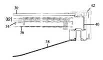
도 3은 종래의 플라즈마 디스플레이의 일측을 개략적으로 나타내는 단면도.3 is a cross-sectional view schematically showing one side of a conventional plasma display.
도 4는 도 3에 도시된 전면필터를 개략적으로 나타내는 단면도.4 is a cross-sectional view schematically showing the front filter shown in FIG.
도 5는 도 3에 도시된 전면필터와 필터 지지부의 접지과정을 상세히 나타내는 도면.5 is a view showing in detail the grounding process of the front filter and the filter support shown in FIG.
도 6은 필름형 전면필터를 개략적으로 나타내는 단면도.6 is a sectional view schematically showing a film type front filter.
도 7a는 종래 전면필터의 투과율곡선을 나타내는 도면.7A is a diagram showing a transmittance curve of a conventional front filter.
도 7b는 종래 전면필터를 위해 설계된 광투과율곡선을 나타내는 도면.Figure 7b is a view showing a light transmittance curve designed for a conventional front filter.
도 8은 본 발명의 제 1 실시예에 따른 전면필터의 투과율곡선을 나타내는 도면.8 is a diagram showing a transmittance curve of a front filter according to a first embodiment of the present invention.
도 9는 본 발명의 제 2 실시예에 따른 전면필터의 투과율곡선을 나타내는 도면.
9 is a diagram showing a transmittance curve of a front filter according to a second embodiment of the present invention.
< 도면의 주요 부분에 대한 부호의 설명 > <Description of Symbols for Main Parts of Drawings>
10 : 상부기판 12Y,12Z : 투명전극10:
13Y,13Z : 버스전극14,22 : 유전체층13Y, 13Z:
16 : 보호막18 : 하부기판16: protective film 18: lower substrate
24 : 격벽26 : 형광체층24: partition 26: phosphor layer
30,60 : 전면필터 32 : 패널30,60
34 : 방열판36 : 인쇄회로기판34: heat sink 36: printed circuit board
38 : 백 커버40 : 필터지지부38: back cover 40: filter support
42 : 지지부재50,62 : 무반사막42:
52,64 : 광특성막54 : 글래스52,64: optical film 54: glass
56,66 : EMI 차폐막58,68 : NIR 차폐막
56,66 EMI
본 발명은 플라즈마 디스플레이 패널에 관한 것으로 특히, 플라즈마 디스플레이 패널의 전면에 부착되는 전면필터에 관한 것이다.The present invention relates to a plasma display panel, and more particularly to a front filter attached to the front surface of the plasma display panel.
플라즈마 디스플레이 패널은 He+Xe, Ne+Xe 또는 He+Ne+Xe 등의 불활성 혼합가스의 방전시 발생하는 147nm의 자외선에 의해 적색, 녹색, 청색을 발광하는 형광 체를 발광시킴으로써 문자 또는 그래픽을 포함한 화상을 표시하게 된다. 이러한 PDP는 박막화와 대형화가 용이할 뿐만 아니라 최근의 기술 개발에 힘입어 크게 향상된 화질을 제공한다. 특히, 3전극 교류 면방전형 PDP는 방전시 표면에 벽전하가 축적되며 방전에 의해 발생되는 스퍼터링으로부터 전극들을 보호하기 때문에 저전압 구동과 장수명의 장점을 가진다.The plasma display panel includes characters or graphics by emitting phosphors emitting red, green, and blue light by ultraviolet rays of 147 nm generated when discharge of an inert mixed gas such as He + Xe, Ne + Xe, or He + Ne + Xe. An image is displayed. Such a PDP is not only thin and easy to enlarge, but also greatly improved in quality due to recent technology development. In particular, the three-electrode AC surface discharge type PDP has advantages of low voltage driving and long life because wall charges are accumulated on the surface during discharge and protect the electrodes from sputtering caused by the discharge.
도 1 은 종래의 플라즈마 디스플레이 패널의 방전셀 구조를 나타내는 사시도이다.1 is a perspective view showing a discharge cell structure of a conventional plasma display panel.
도 1 을 참조하면, 3전극 교류 면방전형 PDP의 방전셀은 상부기판(10) 상에 형성된 스캔전극(Y) 및 서스테인전극(Z)과, 하부기판(18) 상에 형성된 어드레스전극(X)을 구비한다. 스캔전극(Y)과 서스테인전극(Z) 각각은 투명전극(12Y,12Z)과, 투명전극(12Y,12Z)의 선폭보다 작은 선폭을 가지며 투명전극의 일측 가장자리에 형성되는 금속버스전극(13Y,13Z)을 포함한다.Referring to FIG. 1, a discharge cell of a three-electrode AC surface discharge type PDP includes a scan electrode Y and a sustain electrode Z formed on the
투명전극(12Y,12Z)은 통상 인듐틴옥사이드(Indium-Tin-Oxide : ITO)로 상부기판(10) 상에 형성된다. 금속버스전극(13Y,13Z)은 통상 크롬(Cr) 등의 금속으로 투명전극(12Y,12Z) 상에 형성되어 저항이 높은 투명전극(12Y,12Z)에 의한 전압강하를 줄이는 역할을 한다. 스캔전극(Y)과 서스테인전극(Z)이 나란하게 형성된 상부기판(10)에는 상부 유전체층(14)과 보호막(16)이 적층된다. 상부 유전체층(14)에는 플라즈마 방전시 발생된 벽전하가 축적된다. 보호막(16)은 플라즈마 방전시 발생된 스퍼터링에 의한 상부 유전체층(14)의 손상을 방지함과 아울러 2차 전자의 방출 효율을 높이게 된다. 보호막(16)으로는 통상 산화마그네슘(MgO)이 이용된다.The
어드레스전극(X)이 형성된 하부기판(18) 상에는 하부 유전체층(22), 격벽(24)이 형성되며, 하부 유전체층(22)과 격벽(24) 표면에는 형광체층(26)이 도포된다. 어드레스전극(X)은 스캔전극(Y) 및 서스테인전극(Z)과 교차되는 방향으로 형성된다. 격벽(24)은 스트라이프(Stripe) 또는 격자 형태로 형성되어 방전에 의해 생성된 자외선 및 가시광이 인접한 방전셀에 누설되는 것을 방지한다. 형광체층(26)은 플라즈마 방전시 발생된 자외선에 의해 여기되어 적색, 녹색 또는 청색 중 어느 하나의 가시광선을 발생하게 된다. 상/하부기판(10,18)과 격벽(24) 사이에 마련된 방전공간에는 불활성 혼합가스가 주입된다.The lower
PDP는 화상의 계조를 구현하기 위하여, 한 프레임을 발광횟수가 다른 여러 서브필드로 나누어 시분할 구동하게 된다. 각 서브필드는 전화면을 초기화시키기 위한 초기화기간과, 스캔라인을 선택하고 선택된 스캔라인에서 셀을 선택하기 위한 어드레스기간과, 방전횟수에 따라 계조를 구현하는 서스테인기간으로 나누어진다.The PDP is time-divisionally driven by dividing one frame into several subfields having different number of emission times in order to implement grayscale of an image. Each subfield is divided into an initialization period for initializing the full screen, an address period for selecting a scan line and selecting a cell in the selected scan line, and a sustain period for implementing gray levels according to the number of discharges.
예를 들어, 256 계조로 화상을 표시하고자 하는 경우에 도 2와 같이 1/60초에 해당하는 프레임 기간(16.67ms)은 8개의 서브필드들(SF1내지SF8)로 나누어지게 된다. 8개의 서브필드들(SF1내지SF8) 각각은 전술한 바와 같이, 초기화 기간, 어드레스기간과 서스테인기간으로 나누어지게 된다. 각 서브필드의 초기화기간과 어드레스 기간은 각 서브필드마다 동일한 반면에 서스테인 기간은 각 서브필드에서 2n(n=0,1,2,3,4,5,6,7)의 비율로 증가된다.For example, when the image is to be displayed in 256 gray levels, as shown in FIG. 2, the frame period (16.67 ms) corresponding to 1/60 second is divided into eight subfields SF1 to SF8. Each of the eight subfields SF1 to SF8 is divided into an initialization period, an address period, and a sustain period as described above. The initialization period and the address period of each subfield are the same for each subfield, while the sustain period is increased at a rate of 2n (n = 0,1,2,3,4,5,6,7) in each subfield. .
이와 같이 구동되는 PDP에서 상부기판(10) 상에는 전자파를 차폐함과 아울러 외부광의 반사를 방지하기 위하여 전면필터가 설치된다.In the PDP driven as described above, a front filter is installed on the
도 3은 종래의 플라즈마 디스플레이 패널의 일측을 개략적으로 나타내는 단면도이다.3 is a cross-sectional view schematically illustrating one side of a conventional plasma display panel.
도 3을 참조하면, 종래 PDP는 상부기판(10)과 하부기판(18)이 합착되어 형성되는 패널(32)과, 패널(32)의 전면에 설치되는 전면필터(30)와, 패널(32)의 후면에 설치되는 방열판(34)과, 방열판(34)에 부착되도록 설치되는 인쇄회로기판(36)과, PDP의 후면을 감싸도록 형성되는 백 커버(38)와, 전면필터(30)와 백 커버(38)를 접속시키기 위한 필터 지지부(40)와, 필터 지지부(40)를 감싸도록 전면필터(30)와 백 커버(38) 사이에 설치되는 지지부재(42)를 구비한다.Referring to FIG. 3, a conventional PDP includes a
인쇄회로기판(36)은 패널(32)의 전극들로 구동신호를 공급한다. 이를 위해, 인쇄회로기판(36)은 도시되지 않은 다양한 구동부들을 구비한다. 패널(32)은 인쇄회로기판(36)으로부터 공급되는 구동신호에 응답하여 소정의 화상을 표시한다. 방열판(34)은 패널(32) 및 인쇄회로기판(36)으로부터 발생되는 열을 방열시킨다. 백 커버(38)는 외부의 충격으로부터 패널(32)을 보호함과 아울러 후면으로 방출되는 전자파(Electro Magnetic Interference : 이하 "EMI"라 함)를 차단한다.The printed
필터 지지부(40)는 전면필터(30)를 백 커버(38)에 전기적으로 접속시킨다. 이와 같은 필터 지지부(40)는 전면필터(30)를 백 커버(38)에 접지시킴과 아울러 측면으로 EMI가 방출되는 것을 방지한다. 지지부재(42)는 필터 지지부(40), 전면필터(30) 및 백 커버(38) 등을 지지한다.The filter support 40 electrically connects the
전면필터(30)는 EMI를 차폐함과 아울러 외부광의 반사를 방지한다. 이를 위 해, 전면필터(30)는 도 5와 같이 무반사막(50), 광특성 막(52), 글래스(54), EMI 차폐막(56) 및 근적외선(near infrared rays : 이하 "NIR"이라 함) 차폐막(58)을 구비한다. 여기서, 실제로 전면필터(30)의 각 막들(50,52,54,56,58) 사이에는 점착층이 형성되어 각 막들(50,52,54,56,58) 사이를 접착시키게 된다. 또한, 일반적으로 광특성막(52)은 점착층에 특정 물질을 삽입하여 형성된다. 그리고, 전면필터(30)의 구조는 그 제조업체에 따라서 약간씩 변화된다. 본원에서는 설명의 편의성을 위해 점착층을 도시하지 않았으며 광특성막(52)을 특정층으로 표시하였고, 현재 일반적으로 사용되는 전면필터(30)의 구조를 예로 들었다.The
무반사막(Antireflection Coating)(50)은 외부로부터 입사되는 광이 다시 외부로 반사되는 것을 방지하여 PDP의 컨트라스트를 향상시키게 된다. 이와 같은 무반사막(50)은 전면필터(30)의 표면에 형성된다. 한편, 무반사막(50)은 전면필터(30)의 배면에 추가로 형성될 수 있다. 광특성막(52)은 패널(32)로부터 입사되는 광 중 적색(R) 및 녹색(G)의 휘도를 낮춤과 아울러 청색(B)의 휘도를 높여 PDP의 광특성을 개선시킨다.The
글래스(54)는 외부 충격으로부터 전면필터(30)가 파손되는 것을 방지한다. 다시 말하여, 글래스(54)는 전면필터(30)가 외부 충격으로부터 파손되는 것을 방지하도록 전면필터(30)를 지지한다. EMI 차폐막(56)은 EMI를 차폐하여 패널(32)로부터 입사되는 EMI가 외부로 방출되는 것을 방지한다. NIR 차폐막(58)은 패널(32)에서 방사되는 NIR을 차폐하여 리모트 콘트롤러등과 같이 IR을 이용하여 신호를 전달하는 장치들이 신호를 정상적으로 전달할 수 있도록 기준 이상의 NIR이 외부로 방 출되는 것을 방지한다. 한편, EMI 차폐막(56) 및 NIR 차폐막(58)은 하나의 층으로 구성될 수 있다.The
이와 같은 전면필터(30)는 도 5와 같이 필터 지지부(40)를 통하여 백 커버(38)와 전기적으로 접속된다. 이를 상세히 설명하면, 필터 지지부(40)는 전면필터(30)의 일측단에서 전면필터(30)의 배면에 접속된다. 이 때, 필터 지지부(40)는 EMI 차폐막(56) 및 NIR 차폐막(58) 중 적어도 하나 이상의 막과 전기적으로 접속된다. 즉, 필터 지지부(40)는 전면필터(30)를 백 커버(38)에 접속시켜 EMI 및/또는 NIR을 차폐하게 된다.The
이와 같은 종래의 전면필터(30)는 외부로부터의 충격에 의한 전면필터(30)의 파손을 방지하기 위하여 글래스(54)가 이용된다. 하지만, 이와 같이 글래스(54)가 전면필터(30)에 삽입되면 전면필터(30)의 두께가 두꺼워지는 단점이 있다. 또한, 전면필터(30)에 글래스(54)가 삽입되면 그 무게가 무거워짐과 아울러 제조비용이 상승하는 문제점이 있다.The conventional
따라서, 도 6과 같이 글래스(54)를 제거한 필름형 전면필터(60)가 제안되었다. 필름형 전면필터(60)는 무반사막(62), 광특성막(64), EMI 차폐막(66) 및 NIR 차폐막(68)을 구비한다. 여기서, 필름형 전면필터(60)의 각 막들(62,64,66,68) 사이에는 점착층이 형성되어 각 막들(62,64,66,68) 사이를 접착시키게 된다. 그리고, 일반적으로 광특성막(64)은 점착층에 특정 물질을 삽입하여 형성된다. 또한, 필름형 전면필터(60)의 구조는 사용하는 업체에 따라서 약간씩 변화된다. 본원에서는 설명의 편의성을 위해 점착층을 도시하지 않았으며 광특성막(64)을 특정층으 로 표시하였다.Therefore, the film
무반사막(62)은 필름형 전면필터(60)의 표면에 형성되어 외부로부터 입사되는 광이 다시 외부로 반사되는 것을 방지한다. 이와 같은 무반사막(62)은 필름형 전면필터(60)의 배면에 추가로 형성될 수 있다. 광특성막(64)은 패널(32)로부터 입사되는 광 중 적색(R) 및 녹색(G)의 휘도를 낮춤과 아울러 청색(B)의 휘도를 높여 PDP의 광특성을 개선시킨다.The
EMI 차폐막(66)은 EMI를 차폐하여 패널(32)로부터 입사되는 EMI가 외부로 방출되는 것을 방지한다. 이러한 EMI 차폐막(66)은 후술할 NIR 차폐막(68)과 하나의 층으로 구성될 수 있다. The
NIR 차폐막(66)은 패널(32)로부터 입사되는 NIR을 차폐한다. 여기서, NIR은 700~1200nm의 파장영역에 속하는 것으로서 PDP의 패널 내에 충진된 혼합가스 중 방전시 800~1000nm의 선(rays)을 방출하는 Xe에 의해 생성된다. 이러한 NIR이 외부로 방출되면 IR을 사용하여 신호를 전달하는 리모트 컨트롤러 등과 같은 장치의 신호가 PDP에 정상적으로 전달될 수 없게 된다. 즉, NIR의 방출은 리모트 컨트롤러의 오작동을 일으키게 된다. 이에 의해 NIR 차폐막(68)은 리모트 컨트롤러 등으로부터 패널(32)로 전달되는 신호들이 정상적으로 전달될 수 있도록 근적외선 흡수염료를 사용하여 기준 이상의 NIR이 외부로 방출되는 것을 방지한다.The
이와 같은 필름형 전면필터(60)는 글래스(54)를 포함하는 전면필터(30)에 비하여 무게가 가볍고 아울러 박형화할 수 있는 장점이 있다. 또한, 필름형 전면필터(60)는 글래스(54)를 포함한 전면필터(30)에 비하여 제조비용을 절감할 수 있다. 그런데, 종래 필름형 전면필터(60) 및 글래스(54)를 포함하는 전면필터(30)는 도 7a에 도시된 바와 같은 광투과율곡선을 나타낸다. 이러한 전면필터의 광투과율은 전면필터의 각 기능성 층에 포함된 염료와 각 기능성 층의 재질에 영향을 받기도 하지만 도 7b에 도시된 바와 같은 전면필터의 투과율을 결정하기 위한 투과율곡선 설계의 영향도 많이 받게 된다. 도 7a를 참조하면, 종래 전면필터(30,60)는 580 내지 592nm의 영역에 해당하는 오렌지광(73)의 투과율이 40%에 육박하는 등 상당히 높아 적색, 녹색, 청색의 삼원색으로 색을 표현하는 PDP의 색순도를 상당히 저하시키는 문제가 있다. 즉, 적색, 녹색, 청색을 이용하여 흰색을 표현할 때 노란계열로 치우친 흰색으로 나타나거나 살색의 표현이 부적절한 경우가 그것이다. 또한, 525nm에 해당하는 녹색광(72)의 투과율이 청색광(71)이나 적색광(74)에 비해 현저히 낮아 색온도가 저하되는 문제가 있다. 따라서, 전면필터의 투과율 설계를 개선하여 이상적인 투과율을 나타내도록 하는 방안이 필요한 실정이다.Such a film-
따라서, 본 발명의 목적은 이상적인 투과율 곡선을 갖도록 한 전면필터를 제공하는 데 있다.
또한, 본 발명의 다른 목적은 필터의 무게를 줄이고 두께를 얇게하는 전면필터를 제공하는 데 있다.
또한, 본 발명의 또 다른 목적은 필터의 무게를 줄이고 두께를 얇게하는 필터를 제공하는 데 있다.Accordingly, it is an object of the present invention to provide a front filter which has an ideal transmittance curve.
In addition, another object of the present invention to provide a front filter to reduce the weight of the filter and to reduce the thickness.
Another object of the present invention is to provide a filter that reduces the weight of the filter and makes the thickness thinner.
상기 목적을 달성하기 위하여 본 발명의 실시예에 따른 전면필터는 전면필터의 광투과율 곡선에 있어서, 454nm에 해당하는 청색광의 투과율이 50% 내지 80%이 며, 525nm에 해당하는 녹색광의 투과율이 40% 내지 80%이며, 580nm 내지 592nm에 해당하는 오렌지광의 투과율이 5% 내지 30%이며, 610nm 내지 630nm에 해당하는 적색광의 투과율이 50% 내지 80%이며, 850nm 내지 950nm에 해당하는 근적외선의 투과율이 1% 내지 10%인 것을 특징으로 한다.In order to achieve the above object, the front filter according to the embodiment of the present invention has a light transmittance curve of the front filter, wherein the blue light transmittance of 454 nm is 50% to 80%, and the green light transmittance of 40 corresponds to 525 nm. % To 80%, transmittance of orange light corresponding to 580nm to 592nm is 5% to 30%, transmittance of red light corresponding to 610nm to 630nm is 50% to 80%, and transmittance of near infrared ray corresponding to 850nm to 950nm is It is characterized in that 1% to 10%.
본 발명의 실시예에 따른 전면필터의 광투과율 곡선에 있어서, 454nm에 해당하는 청색광의 투과율이 60% 내지 70%이며, 525nm에 해당하는 녹색광의 투과율이 60% 내지 70%이며, 580nm 내지 592nm에 해당하는 오렌지광의 투과율이 5% 내지 20%이며, 610nm 내지 630nm에 해당하는 적색광의 투과율이 60% 내지 70%이며, 850nm 내지 950nm에 해당하는 근적외선의 투과율이 1% 내지 5%인 것을 특징으로 한다.In the light transmittance curve of the front filter according to the embodiment of the present invention, the transmittance of blue light corresponding to 454 nm is 60% to 70%, the transmittance of green light corresponding to 525nm is 60% to 70%, and is from 580nm to 592nm. The transmittance of the corresponding orange light is 5% to 20%, the transmittance of the red light corresponding to 610nm to 630nm is 60% to 70%, and the near-infrared transmittance of 850nm to 950nm is 1% to 5%. .
상기 청색광 및 상기 녹색광 사이 영역에 해당하는 빛의 투과율은 상기 청색광 및 상기 녹색광의 투과율에 비해 1% 내지 20% 감소되며, 상기 녹색광 및 상기 적색광 사이 영역에 해당하는 빛의 투과율은 상기 녹색광 및 상기 적색광의 투과율에 비해 10% 내지 30% 감소되며, 상기 적색광 및 상기 근적외선 사이 영역에 해당하는 빛의 투과율은 상기 적색광의 투과율에 비해 1% 내지 70% 감소되는 것을 특징으로 한다.The transmittance of light corresponding to the region between the blue light and the green light is reduced by 1% to 20% compared to the transmittance of the blue light and the green light, and the transmittance of light corresponding to the region between the green light and the red light is the green light and the red light. 10% to 30% is reduced compared to the transmittance of, and the transmittance of light corresponding to the region between the red light and the near infrared is characterized in that 1% to 70% reduced compared to the transmittance of the red light.
상기 청색광 및 상기 녹색광 사이 영역에 해당하는 빛의 흡수피크는 480nm 내지 500nm의 영역에서 형성되며, 상기 녹색광 및 상기 적색광 사이 영역에 해당하는 빛의 흡수피크는 580nm 내지 600nm의 영역에서 형성되며, 상기 적색광 및 상기 근적외선 사이 영역에 해당하는 빛의 흡수피크는 640nm 내지 700nm의 영역에서 형성되는 것을 특징으로 한다.The absorption peak of light corresponding to the region between the blue light and the green light is formed in the region of 480 nm to 500 nm, and the absorption peak of light corresponding to the region between the green and red light is formed in the region of 580 nm to 600 nm, and the red light And an absorption peak of light corresponding to the region between the near infrared rays is formed in the region of 640nm to 700nm.
상기 목적 외에 본 발명의 다른 목적 및 특징들은 첨부도면을 참조한 실시예에 대한 설명을 통하여 명백하게 드러나게 될 것이다.Other objects and features of the present invention in addition to the above objects will become apparent from the description of the embodiments with reference to the accompanying drawings.
이하 도 8 내지 도 9를 참조하여 본 발명의 바람직한 실시예에 대하여 설명하기로 한다.Hereinafter, exemplary embodiments of the present invention will be described with reference to FIGS. 8 to 9.
도 8은 본 발명의 제 1 실시예에 의한 플라즈마 디스플레이 패널의 전면필터의 광투과율 곡선을 나타내는 도면이다.8 is a view showing a light transmittance curve of the front filter of the plasma display panel according to the first embodiment of the present invention.
도 8을 참조하면, 본 발명의 제 1 실시예에 따른 전면필터의 광투과율 곡선은 454nm에 해당하는 청색광(81)의 투과율이 50% 내지 80%이며, 525nm에 해당하는 녹색광(82)의 투과율이 40% 내지 80%이며, 580nm 내지 592nm에 해당하는 오렌지광(83)의 투과율이 5% 내지 30%이며, 610nm 내지 630nm에 해당하는 적색광(84)의 투과율이 50% 내지 80%이며, 850nm 내지 950nm에 해당하는 근적외선(85)의 투과율이 1% 내지 10%이다.Referring to FIG. 8, the light transmittance curve of the front filter according to the first embodiment of the present invention has a transmittance of 50% to 80% of the blue light 81 corresponding to 454nm, and a transmittance of the green light 82 corresponding to 525nm. 40% to 80%, the transmittance of the orange light 83 corresponding to 580nm to 592nm is 5% to 30%, the transmittance of the red light 84 corresponding to 610nm to 630nm is 50% to 80%, 850nm The transmittance of the near infrared ray 85 corresponding to 950 nm is 1%-10%.
이는 종래에 비해 녹색광(82)의 투과율을 20% 내지 30% 상승하여 색온도를 현저히 증가시키며, 오렌지광(83)의 투과율을 20% 내지 30% 감소시켜 색순도를 현저히 상승시키게 된다. 아울러, 근적외선(85) 부근의 곡선 기울기를 크게 함으로써 원격조정장치의 오작동을 유발시키는 근적외선(85) 투과율도 종래에 비해 큰 폭으로 감소시킬 수 있게 된다.This significantly increases the color temperature by increasing the transmittance of the green light 82 by 20% to 30% compared to the conventional art, and significantly increases the color purity by reducing the transmittance of the orange light 83 by 20% to 30%. In addition, by increasing the slope of the curve near the near infrared ray 85, the transmittance of the near infrared ray 85, which causes a malfunction of the remote control device, can be greatly reduced as compared with the related art.
그결과, 본 발명의 제 1 실시예에 따른 전면필터는 이상적인 광투과율 곡선을 나타냄으로써 PDP의 색순도를 개선하고 컨트라스트를 증가시키며 색온도를 증가시키는 효과를 나타내게 된다.As a result, the front filter according to the first embodiment of the present invention exhibits an ideal light transmittance curve, thereby improving color purity of PDP, increasing contrast, and increasing color temperature.
도 9는 본 발명의 제 2 실시예에 의한 플라즈마 디스플레이 패널의 전면필터의 광투과율 곡선을 나타내는 도면이다.9 is a view showing a light transmittance curve of the front filter of the plasma display panel according to the second embodiment of the present invention.
도 9를 참조하면, 본 발명의 제 2 실시예에 따른 전면필터의 광투과율 곡선은 454nm에 해당하는 청색광(91)의 투과율이 60% 내지 70%이며, 525nm에 해당하는 녹색광(92)의 투과율이 60% 내지 70%이며, 580nm 내지 592nm에 해당하는 오렌지광(93)의 투과율이 5% 내지 20%이며, 610nm 내지 630nm에 해당하는 적색광(94)의 투과율이 60% 내지 70%이며, 850nm 내지 950nm에 해당하는 근적외선(95)의 투과율이 1% 내지 5%이다.9, the light transmittance curve of the front filter according to the second exemplary embodiment of the present invention has a transmittance of 60% to 70% of the blue light 91 corresponding to 454nm and a transmittance of the
또한, 본 발명의 제 2 실시예에 따른 전면필터의 광투과율 곡선은 청색광(91) 및 녹색광(92) 사이에 위치하는 계곡인 청녹 사이의 흡수피크(96)를 480nm 내지 500nm의 영역에서 깊게 형성하여 청색광(91) 및 녹색광(92)의 투과율과 1% 내지 20% 차이나도록 하며, 녹색광(92) 및 적색광(94) 사이에 위치하는 계곡인 녹적 사이의 흡수피크(93)를 580nm 내지 600nm의 영역에서 깊게 형성하여 녹색광(92) 및 적색광(94)의 투과율과 10% 내지 30% 차이나도록 한다. 또한, 적색광(95) 및 근적외선(95) 사이의 투과율 차이를 1% 내지 70% 정도로 차이나도록 근적외선 흡수피크(97)를 640nm 내지 700nm의 영역에서 깊게 형성하여 근적외선(95)의 투과를 현저히 감소시킨다.Further, the light transmittance curve of the front filter according to the second embodiment of the present invention deeply forms an
이는 종래에 비해 녹색광(92)의 투과율을 20% 내지 30% 상승하여 색온도를 현저히 증가시키며, 오렌지광(93)의 투과율을 20% 내지 30% 감소시켜 색순도를 현저히 상승시키게 된다. 또한, 근적외선(95) 부근의 곡선 기울기를 크게 함으로써 원격조정장치의 오작동을 유발시키는 근적외선(95) 투과율도 종래에 비해 큰 폭으로 감소시킬 수 있게 된다. 아울러, 청색광(91) 및 녹색광(92) 사이의 흡수피크(96)가 480nm 내지 500nm에 위치하도록 함으로써 색순도가 낮은 파장대의 광투과율을 현저히 감소시켜 청색 및 녹색광의 색순도를 높이게 된다.This significantly increases the color temperature by increasing the transmittance of the
그결과, 본 발명의 제 2 실시예에 따른 전면필터는 적색, 녹색, 청색 각각의 빛을 색순도가 높은 파장의 빛들만 투과시켜 이상적인 광투과율 곡선을 나타냄으로써 PDP의 색순도를 개선할 수 있게 된다. 또한, PDP의 형광체에서 발광되는 삼원색의 빛을 제외한 나머지 파장대의 빛들의 투과율을 현저히 감소시킴으로써 명실 컨트라스트를 증가시킨다. 더욱이, 녹색광의 투과율을 증가시킴으로써 PDP의 색온도를 증가시키는 효과를 나타내게 된다.
As a result, the front filter according to the second embodiment of the present invention can improve the color purity of the PDP by displaying the ideal light transmittance curve by transmitting only the light having a high color purity wavelength of each of red, green, and blue light. In addition, by reducing the transmittance of the light of the remaining wavelength band except for the three primary colors emitted from the phosphor of the PDP significantly increases the clear contrast. Furthermore, increasing the transmittance of green light has the effect of increasing the color temperature of the PDP.
상술한 바와 같이, 본 발명에 따른 전면필터는 이상적인 광투과율 곡선을 나타내도록 함으로써 PDP의 색순도를 개선할 수 있게 된다. 또한, PDP의 형광체에서 발광되는 삼원색의 빛을 제외한 나머지 파장대의 빛들의 투과율을 현저히 감소시킴으로써 명실 컨트라스트를 증가시키며 녹색광의 투과율을 증가시킴으로써 PDP의 색온도를 증가시키는 효과를 나타내게 된다.
또한, 본 발명에 따른 필터는 글래스 층을 사용하지 않고, 근적외선 차폐막, 전자파 차폐막, 광특성막 및 무반사막을 사용하여 필터를 구성함으로써 필터의 두께를 얇게하고 무게를 줄이는 효과를 나타내게 된다.
또한, 본 발명에 따른 전면필터는 글래스 층을 사용하지 않고, 근적외선 차폐막, 전자파 차폐막, 광특성막 및 무반사막을 사용하여 필터를 구성함으로써 전면필터의 두께를 얇게하고 무게를 줄이는 효과를 나타내게 된다.As described above, the front filter according to the present invention can improve the color purity of the PDP by showing an ideal light transmittance curve. In addition, by significantly reducing the transmittance of the light of the wavelength band except for the three primary colors emitted from the phosphor of the PDP to increase the clear contrast and to increase the color temperature of the PDP by increasing the transmittance of the green light.
In addition, the filter according to the present invention exhibits the effect of reducing the thickness and weight of the filter by constructing the filter using a near infrared shielding film, an electromagnetic shielding film, an optical characteristic film, and an antireflective film without using a glass layer.
In addition, the front filter according to the present invention exhibits the effect of reducing the thickness and weight of the front filter by configuring the filter using a near infrared shielding film, an electromagnetic shielding film, an optical characteristic film, and an antireflection film without using a glass layer.
이상 설명한 내용을 통해 당업자라면 본 발명의 기술사상을 일탈하지 않는 범위에서 다양한 변경 및 수정이 가능함으로 알 수 있을 것이다. 따라서, 본 발명의 기술적 범위는 명세서의 상세한 설명에 기재된 내용으로 한정되는 것이 아니라 특허 청구의 범위에 의해 정하여져야만 할 것이다.
Those skilled in the art will appreciate that various changes and modifications can be made without departing from the technical spirit of the present invention. Therefore, the technical scope of the present invention should not be limited to the contents described in the detailed description of the specification but should be defined by the claims.
Claims (6)
Translated fromKoreanPriority Applications (4)
| Application Number | Priority Date | Filing Date | Title |
|---|---|---|---|
| KR1020030008838AKR100764761B1 (en) | 2003-02-12 | 2003-02-12 | Front filter |
| US10/778,462US7218044B2 (en) | 2003-02-12 | 2004-02-12 | Front filter in plasma display panel |
| JP2004035636AJP2004246364A (en) | 2003-02-12 | 2004-02-12 | Front filter of plasma display panel |
| US11/697,221US20070188854A1 (en) | 2003-02-12 | 2007-04-05 | Front filter in plasma display panel |
Applications Claiming Priority (1)
| Application Number | Priority Date | Filing Date | Title |
|---|---|---|---|
| KR1020030008838AKR100764761B1 (en) | 2003-02-12 | 2003-02-12 | Front filter |
Publications (2)
| Publication Number | Publication Date |
|---|---|
| KR20040072375A KR20040072375A (en) | 2004-08-18 |
| KR100764761B1true KR100764761B1 (en) | 2007-10-11 |
Family
ID=32866881
Family Applications (1)
| Application Number | Title | Priority Date | Filing Date |
|---|---|---|---|
| KR1020030008838AExpired - Fee RelatedKR100764761B1 (en) | 2003-02-12 | 2003-02-12 | Front filter |
Country Status (3)
| Country | Link |
|---|---|
| US (2) | US7218044B2 (en) |
| JP (1) | JP2004246364A (en) |
| KR (1) | KR100764761B1 (en) |
Families Citing this family (14)
| Publication number | Priority date | Publication date | Assignee | Title |
|---|---|---|---|---|
| KR100764761B1 (en)* | 2003-02-12 | 2007-10-11 | 엘지전자 주식회사 | Front filter |
| KR100751932B1 (en)* | 2003-04-01 | 2007-08-27 | 엘지전자 주식회사 | Front filter and its manufacturing method |
| KR20060084586A (en)* | 2005-01-20 | 2006-07-25 | 삼성에스디아이 주식회사 | Plasma display device |
| KR20070056359A (en) | 2005-11-29 | 2007-06-04 | 엘지전자 주식회사 | Plasma display device |
| JP5313347B2 (en)* | 2009-06-25 | 2013-10-09 | パナソニック株式会社 | Multicolor organic EL display device and method for manufacturing the same |
| US10642087B2 (en) | 2014-05-23 | 2020-05-05 | Eyesafe, Llc | Light emission reducing compounds for electronic devices |
| CA2995631A1 (en)* | 2014-05-23 | 2015-11-26 | Healthe Llc | Light emission reducing film for electronic devices |
| US10901125B2 (en) | 2014-05-23 | 2021-01-26 | Eyesafe, Llc | Light emission reducing compounds for electronic devices |
| US11592701B2 (en) | 2018-11-28 | 2023-02-28 | Eyesafe Inc. | Backlight unit with emission modification |
| US10955697B2 (en) | 2018-11-28 | 2021-03-23 | Eyesafe Inc. | Light emission modification |
| US12321060B1 (en) | 2018-11-28 | 2025-06-03 | Eyesafe Inc. | Color filter enhancements for display devices |
| US11126033B2 (en) | 2018-11-28 | 2021-09-21 | Eyesafe Inc. | Backlight unit with emission modification |
| US11810532B2 (en) | 2018-11-28 | 2023-11-07 | Eyesafe Inc. | Systems for monitoring and regulating harmful blue light exposure from digital devices |
| US10971660B2 (en) | 2019-08-09 | 2021-04-06 | Eyesafe Inc. | White LED light source and method of making same |
Citations (2)
| Publication number | Priority date | Publication date | Assignee | Title |
|---|---|---|---|---|
| JP2001194524A (en)* | 2000-01-13 | 2001-07-19 | Fuji Photo Film Co Ltd | Optical filter, front plate and picture display device using same |
| KR20010095783A (en)* | 2000-04-12 | 2001-11-07 | 구자홍 | plasma display panel and manufacturing method there of |
Family Cites Families (15)
| Publication number | Priority date | Publication date | Assignee | Title |
|---|---|---|---|---|
| US6013983A (en)* | 1995-12-28 | 2000-01-11 | Dai Nippon Printing Co., Ltd. | Transparent colored conductive film |
| US6255031B1 (en)* | 1996-04-18 | 2001-07-03 | Kanebo, Ltd. | Near infrared absorbing film, and multi-layered panel comprising the film |
| JPH1027550A (en)* | 1996-05-09 | 1998-01-27 | Pioneer Electron Corp | Plasma display panel |
| JP3145309B2 (en)* | 1996-06-12 | 2001-03-12 | 富士通株式会社 | Method of preventing near-infrared emission from flat display device and plasma display panel |
| US6531230B1 (en)* | 1998-01-13 | 2003-03-11 | 3M Innovative Properties Company | Color shifting film |
| JPH11307987A (en)* | 1998-04-16 | 1999-11-05 | Nippon Sheet Glass Co Ltd | Electromagnetic wave filter |
| JP3576032B2 (en)* | 1999-03-31 | 2004-10-13 | 富士通株式会社 | Gas discharge display |
| JP2000294980A (en)* | 1999-04-06 | 2000-10-20 | Nippon Sheet Glass Co Ltd | Translucent electromagnetic wave filter and method of manufacturing the same |
| KR20040020922A (en)* | 2001-06-12 | 2004-03-09 | 미쓰비시 가가꾸 가부시키가이샤 | Electronic display-use filter and electronic display unit using the filter |
| DE60232603D1 (en)* | 2001-06-21 | 2009-07-23 | Teijin Ltd | Near-PROTECTION |
| KR100455121B1 (en)* | 2002-02-20 | 2004-11-06 | 엘지전자 주식회사 | Manufacturing method for front panel dielectiric of plasma display panel |
| KR100764761B1 (en)* | 2003-02-12 | 2007-10-11 | 엘지전자 주식회사 | Front filter |
| KR100751932B1 (en)* | 2003-04-01 | 2007-08-27 | 엘지전자 주식회사 | Front filter and its manufacturing method |
| JP4744098B2 (en)* | 2004-05-18 | 2011-08-10 | パナソニック株式会社 | Display device, plasma display device, and optical filter |
| TWI266902B (en)* | 2005-01-19 | 2006-11-21 | Lg Chemical Ltd | Filter for plasma display panel with good re-workability and plasma display panel comprising the same |
- 2003
- 2003-02-12KRKR1020030008838Apatent/KR100764761B1/ennot_activeExpired - Fee Related
- 2004
- 2004-02-12USUS10/778,462patent/US7218044B2/ennot_activeExpired - Fee Related
- 2004-02-12JPJP2004035636Apatent/JP2004246364A/enactivePending
- 2007
- 2007-04-05USUS11/697,221patent/US20070188854A1/ennot_activeAbandoned
Patent Citations (2)
| Publication number | Priority date | Publication date | Assignee | Title |
|---|---|---|---|---|
| JP2001194524A (en)* | 2000-01-13 | 2001-07-19 | Fuji Photo Film Co Ltd | Optical filter, front plate and picture display device using same |
| KR20010095783A (en)* | 2000-04-12 | 2001-11-07 | 구자홍 | plasma display panel and manufacturing method there of |
Also Published As
| Publication number | Publication date |
|---|---|
| KR20040072375A (en) | 2004-08-18 |
| US20070188854A1 (en) | 2007-08-16 |
| US20040164661A1 (en) | 2004-08-26 |
| US7218044B2 (en) | 2007-05-15 |
| JP2004246364A (en) | 2004-09-02 |
Similar Documents
| Publication | Publication Date | Title |
|---|---|---|
| KR100945428B1 (en) | Front-filter | |
| KR100509763B1 (en) | Front filter of plasma display panel | |
| KR100499062B1 (en) | Plasma display panel | |
| KR100764761B1 (en) | Front filter | |
| KR20040085699A (en) | Front filter of plasma display panel | |
| KR100764762B1 (en) | Plasma display panel | |
| KR100911034B1 (en) | Front filter of plasma display panel | |
| KR100516935B1 (en) | Plasma display panel | |
| KR100516939B1 (en) | Plasma display panel | |
| KR100546260B1 (en) | Plasma display panel module | |
| KR100508239B1 (en) | Plasma display panel | |
| KR100505988B1 (en) | Film Type Filter for Plasma Display Panel | |
| KR100516940B1 (en) | Plasma display panel | |
| KR100499061B1 (en) | Plasma display panel | |
| KR100505979B1 (en) | Front filter of plasma display panel | |
| US20060279211A1 (en) | Plasma display panel | |
| KR20040072376A (en) | Front-filter | |
| KR100682360B1 (en) | Plasma display panel | |
| KR100718051B1 (en) | Plasma Display Panel And Method Of Manufacturing The Same | |
| KR20040064761A (en) | Base film of front filter | |
| KR20040061893A (en) | Plasma display panel | |
| KR100748956B1 (en) | Plasma Display Panel And Filter Manufacturing Method | |
| KR100775847B1 (en) | Plasma Display Panel | |
| KR20040080157A (en) | Plasma display panel with front-filter of film type | |
| KR20050045624A (en) | Plasma display panel module |
Legal Events
| Date | Code | Title | Description |
|---|---|---|---|
| PA0109 | Patent application | St.27 status event code:A-0-1-A10-A12-nap-PA0109 | |
| P11-X000 | Amendment of application requested | St.27 status event code:A-2-2-P10-P11-nap-X000 | |
| P13-X000 | Application amended | St.27 status event code:A-2-2-P10-P13-nap-X000 | |
| R15-X000 | Change to inventor requested | St.27 status event code:A-3-3-R10-R15-oth-X000 | |
| R16-X000 | Change to inventor recorded | St.27 status event code:A-3-3-R10-R16-oth-X000 | |
| R18-X000 | Changes to party contact information recorded | St.27 status event code:A-3-3-R10-R18-oth-X000 | |
| PG1501 | Laying open of application | St.27 status event code:A-1-1-Q10-Q12-nap-PG1501 | |
| R17-X000 | Change to representative recorded | St.27 status event code:A-3-3-R10-R17-oth-X000 | |
| A201 | Request for examination | ||
| A302 | Request for accelerated examination | ||
| P11-X000 | Amendment of application requested | St.27 status event code:A-2-2-P10-P11-nap-X000 | |
| P13-X000 | Application amended | St.27 status event code:A-2-2-P10-P13-nap-X000 | |
| PA0201 | Request for examination | St.27 status event code:A-1-2-D10-D11-exm-PA0201 | |
| PA0302 | Request for accelerated examination | St.27 status event code:A-1-2-D10-D17-exm-PA0302 St.27 status event code:A-1-2-D10-D16-exm-PA0302 | |
| E902 | Notification of reason for refusal | ||
| PE0902 | Notice of grounds for rejection | St.27 status event code:A-1-2-D10-D21-exm-PE0902 | |
| P11-X000 | Amendment of application requested | St.27 status event code:A-2-2-P10-P11-nap-X000 | |
| P13-X000 | Application amended | St.27 status event code:A-2-2-P10-P13-nap-X000 | |
| E902 | Notification of reason for refusal | ||
| PE0902 | Notice of grounds for rejection | St.27 status event code:A-1-2-D10-D21-exm-PE0902 | |
| E13-X000 | Pre-grant limitation requested | St.27 status event code:A-2-3-E10-E13-lim-X000 | |
| P11-X000 | Amendment of application requested | St.27 status event code:A-2-2-P10-P11-nap-X000 | |
| P13-X000 | Application amended | St.27 status event code:A-2-2-P10-P13-nap-X000 | |
| E701 | Decision to grant or registration of patent right | ||
| PE0701 | Decision of registration | St.27 status event code:A-1-2-D10-D22-exm-PE0701 | |
| GRNT | Written decision to grant | ||
| PR0701 | Registration of establishment | St.27 status event code:A-2-4-F10-F11-exm-PR0701 | |
| PR1002 | Payment of registration fee | St.27 status event code:A-2-2-U10-U11-oth-PR1002 Fee payment year number:1 | |
| PG1601 | Publication of registration | St.27 status event code:A-4-4-Q10-Q13-nap-PG1601 | |
| PN2301 | Change of applicant | St.27 status event code:A-5-5-R10-R13-asn-PN2301 St.27 status event code:A-5-5-R10-R11-asn-PN2301 | |
| R18-X000 | Changes to party contact information recorded | St.27 status event code:A-5-5-R10-R18-oth-X000 | |
| R18-X000 | Changes to party contact information recorded | St.27 status event code:A-5-5-R10-R18-oth-X000 | |
| LAPS | Lapse due to unpaid annual fee | ||
| PC1903 | Unpaid annual fee | St.27 status event code:A-4-4-U10-U13-oth-PC1903 Not in force date:20101002 Payment event data comment text:Termination Category : DEFAULT_OF_REGISTRATION_FEE | |
| PC1903 | Unpaid annual fee | St.27 status event code:N-4-6-H10-H13-oth-PC1903 Ip right cessation event data comment text:Termination Category : DEFAULT_OF_REGISTRATION_FEE Not in force date:20101002 | |
| P22-X000 | Classification modified | St.27 status event code:A-4-4-P10-P22-nap-X000 | |
| PN2301 | Change of applicant | St.27 status event code:A-5-5-R10-R13-asn-PN2301 St.27 status event code:A-5-5-R10-R11-asn-PN2301 | |
| PN2301 | Change of applicant | St.27 status event code:A-5-5-R10-R13-asn-PN2301 St.27 status event code:A-5-5-R10-R11-asn-PN2301 |