KR100763224B1 - Semiconductor device and manufacturing method thereof - Google Patents
Semiconductor device and manufacturing method thereofDownload PDFInfo
- Publication number
- KR100763224B1 KR100763224B1KR1020060012193AKR20060012193AKR100763224B1KR 100763224 B1KR100763224 B1KR 100763224B1KR 1020060012193 AKR1020060012193 AKR 1020060012193AKR 20060012193 AKR20060012193 AKR 20060012193AKR 100763224 B1KR100763224 B1KR 100763224B1
- Authority
- KR
- South Korea
- Prior art keywords
- inductor
- film
- forming
- layer
- polyimide film
- Prior art date
- Legal status (The legal status is an assumption and is not a legal conclusion. Google has not performed a legal analysis and makes no representation as to the accuracy of the status listed.)
- Active
Links
Images


Classifications
- H—ELECTRICITY
- H01—ELECTRIC ELEMENTS
- H01L—SEMICONDUCTOR DEVICES NOT COVERED BY CLASS H10
- H01L23/00—Details of semiconductor or other solid state devices
- H01L23/52—Arrangements for conducting electric current within the device in operation from one component to another, i.e. interconnections, e.g. wires, lead frames
- H01L23/522—Arrangements for conducting electric current within the device in operation from one component to another, i.e. interconnections, e.g. wires, lead frames including external interconnections consisting of a multilayer structure of conductive and insulating layers inseparably formed on the semiconductor body
- H01L23/5227—Inductive arrangements or effects of, or between, wiring layers
- H—ELECTRICITY
- H10—SEMICONDUCTOR DEVICES; ELECTRIC SOLID-STATE DEVICES NOT OTHERWISE PROVIDED FOR
- H10D—INORGANIC ELECTRIC SEMICONDUCTOR DEVICES
- H10D84/00—Integrated devices formed in or on semiconductor substrates that comprise only semiconducting layers, e.g. on Si wafers or on GaAs-on-Si wafers
- H—ELECTRICITY
- H10—SEMICONDUCTOR DEVICES; ELECTRIC SOLID-STATE DEVICES NOT OTHERWISE PROVIDED FOR
- H10D—INORGANIC ELECTRIC SEMICONDUCTOR DEVICES
- H10D1/00—Resistors, capacitors or inductors
- H10D1/20—Inductors
- H—ELECTRICITY
- H01—ELECTRIC ELEMENTS
- H01L—SEMICONDUCTOR DEVICES NOT COVERED BY CLASS H10
- H01L2924/00—Indexing scheme for arrangements or methods for connecting or disconnecting semiconductor or solid-state bodies as covered by H01L24/00
- H01L2924/0001—Technical content checked by a classifier
- H01L2924/0002—Not covered by any one of groups H01L24/00, H01L24/00 and H01L2224/00
Landscapes
- Physics & Mathematics (AREA)
- Condensed Matter Physics & Semiconductors (AREA)
- General Physics & Mathematics (AREA)
- Engineering & Computer Science (AREA)
- Computer Hardware Design (AREA)
- Microelectronics & Electronic Packaging (AREA)
- Power Engineering (AREA)
- Semiconductor Integrated Circuits (AREA)
- Internal Circuitry In Semiconductor Integrated Circuit Devices (AREA)
Abstract
Translated fromKoreanDescription
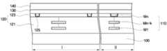
Translated fromKorean도 1은 본 발명의 일 실시예에 따른 반도체 소자의 단면도이다.1 is a cross-sectional view of a semiconductor device in accordance with an embodiment of the present invention.
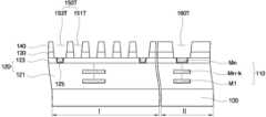
도 2는 본 발명의 다른 실시예에 따른 반도체 소자의 단면도이다.2 is a cross-sectional view of a semiconductor device according to another embodiment of the present invention.
도 3은 본 발명의 또 다른 실시예에 따른 반도체 장치의 단면도이다.3 is a cross-sectional view of a semiconductor device according to still another embodiment of the present invention.
도 4a 내지 도 4e는 도 1에 도시된 반도체 장치의 제조 공정을 순차적으로 나타낸 단면도들이다.4A through 4E are cross-sectional views sequentially illustrating a process of manufacturing the semiconductor device illustrated in FIG. 1.
도 5a 내지 도 5b는 도 2에 도시된 반도체 장치의 제조 공정을 순차적으로 나타낸 단면도들이다.5A through 5B are cross-sectional views sequentially illustrating a manufacturing process of the semiconductor device illustrated in FIG. 2.
도 6은 도 3에 도시된 반도체 장치의 제조 공정을 설명하기 위한 단면도이다.FIG. 6 is a cross-sectional view for describing a manufacturing process of the semiconductor device illustrated in FIG. 3.
(도면의 주요부분에 대한 부호의 설명)(Explanation of symbols for the main parts of the drawing)
I: 인덕터 형성 영역II: 패드 형성 영역I: Inductor Formation Region II: Pad Formation Region
100: 반도체 기판110 : 다층 배선 구조100: semiconductor substrate 110: multilayer wiring structure
120 : 층간 절연막121: 하부 층간 절연막120: interlayer insulating film 121: lower interlayer insulating film
123 : 최상 층간 절연막125 : 최상 금속층123: best interlayer insulating film 125: best metal layer
130 : 패시베이션막140 : 제1 폴리이미드막130: passivation film 140: first polyimide film
150 : 인덕터160: 금속 패드막150: inductor 160: metal pad film
170: 본딩 패드180: 제2 폴리이미드막170: bonding pad 180: second polyimide film
B: 배리어막B: barrier film
본 발명은 반도체 장치 및 그 제조 방법에 관한 것으로, 보다 상세하게는 성능이 향상된 인덕터를 포함하는 반도체 장치 및 그의 제조 방법에 관한 것이다.The present invention relates to a semiconductor device and a manufacturing method thereof, and more particularly, to a semiconductor device including an inductor with improved performance and a manufacturing method thereof.
SOC(system on a chip)는 시스템 LSI(Large Scale Integrated circuit) 혹은 시스템 IC(Integrated Circuit) 등으로 불리워지는데, 이것은 인쇄 회로 기판(Printed Circuit Board: PCB) 상에 구성하던 시스템을 하나의 반도체 상에 집적시켜 하나의 칩(one chip)으로 구현한 것이다. 즉, SOC는 한 개의 칩 상에 완전한 구동 가능한 제품이 들어있는 것을 말한다. 예를 들면, 통신에 사용되는 SOC에는 마이크로프로세서, DSP, 램과 롬 등이 함께 포함될 수 있다. 이러한 SOC를 이용하면 종래에 비하여 시스템의 크기가 작아질 뿐만 아니라 조립 과정도 단순해질 수 있어, 최근 이에 대한 시도가 많이 이루어지고 있다.A system on a chip (SOC) is called a system large scale integrated circuit (LSI) or system integrated circuit (IC), which is a system on a printed circuit board (PCB). It is integrated into one chip. In other words, an SOC is a product that is fully operational on one chip. For example, an SOC used for communication may include a microprocessor, DSP, RAM, and ROM. The use of such an SOC not only reduces the size of the system but also simplifies the assembly process as compared with the prior art, and many attempts have been made recently.
일반적으로 SOC는 종래의 반도체 소자와 RF 회로 소자를 하나의 칩으로 구현한다. RF 대역에서 사용되는 혼재 신호 회로(mixed signal circuit)가 실리콘 베이스(silicon base)의 반도체 기판상에 형성되는 추세이며, 이러한 회로는 기본적인 수동(passive) 소자인 저항(resistor), 커패시터(capacitor), 인덕터(inductor) 등 을 사용한다.In general, an SOC implements a conventional semiconductor device and an RF circuit device as one chip. Mixed signal circuits used in the RF band are formed on a silicon base semiconductor substrate, and these circuits are the basic passive elements such as resistors, capacitors, Use an inductor or the like.
특히, 수동 소자 중 가장 큰 면적을 차지하는 인덕터의 경우는 높은 성능, 즉 인덕턴스(inductance L) 및 에너지 축적 능력을 결정하는 Q 계수(quality factor)의 높은 성능이 요구된다. 특히 Q 계수가 높을수록 전압 제어 발진기와 대역 통과 필터의 주파수 특성이 안정화되고, 손실이 줄어들 수 있다. 여기서, 인덕턴스는 주로 인덕터의 금속 배선의 길이에 의해 결정되고, Q 계수는 금속의 저항에 의해 주로 결정된다. In particular, the inductor occupying the largest area among the passive devices requires high performance, that is, high performance of a Q factor that determines inductance and energy storage capacity. In particular, the higher the Q coefficient, the more stable the frequency characteristics of the voltage-controlled oscillator and bandpass filter and the less the loss can be. Here, the inductance is mainly determined by the length of the metal wiring of the inductor, and the Q coefficient is mainly determined by the resistance of the metal.
그런데, 종래에는 RF CMOS 공정이나 일반 로직 공정에서 주로 최상층 금속 배선을 인덕터로 사용하고 있다. 이러한 경우는 최상층 금속 배선의 길이를 충분히 연장하거나 두께를 증가시키는 것은 공정상 한계가 있어, 높은 저항으로 인하여 인덕터의 성능을 개선하는데 어려움이 있다.However, conventionally, the uppermost metal wiring is mainly used as an inductor in an RF CMOS process or a general logic process. In such a case, it is difficult to fully extend the length or increase the thickness of the uppermost metal wiring, thereby improving the performance of the inductor due to high resistance.
본 발명이 이루고자 하는 기술적 과제는, 성능이 향상된 인덕터를 포함하는 반도체 장치를 제공하는 것이다.An object of the present invention is to provide a semiconductor device including an inductor having improved performance.
본 발명이 이루고자 하는 다른 기술적 과제는, 전술한 반도체 장치를 제조하는 방법을 제공하는 것이다.Another object of the present invention is to provide a method of manufacturing the semiconductor device described above.
본 발명의 기술적 과제들은 이상에서 언급한 기술적 과제로 제한되지 않으며, 언급되지 않은 또 다른 기술적 과제들은 아래의 기재로부터 당업자에게 명확하게 이해될 수 있을 것이다.Technical problems of the present invention are not limited to the technical problems mentioned above, and other technical problems not mentioned will be clearly understood by those skilled in the art from the following description.
상기 기술적 과제를 달성하기 위한 본 발명의 일 실시예에 따른 반도체 장치는 반도체 기판, 상기 반도체 기판 상에 형성된 다층 배선 구조, 상기 다층 배선 구조의 최상 배선층을 덮는 패시베이션막, 상기 패시베이션막 상에 형성된 제1 폴리이미드막 및 상기 패시베이션막 및 상기 제1 폴리이미드막 내에 형성된 인덕터를 포함한다.According to an aspect of the present invention, a semiconductor device includes a semiconductor substrate, a multilayer wiring structure formed on the semiconductor substrate, a passivation film covering an uppermost wiring layer of the multilayer wiring structure, and a passivation film formed on the passivation film. And an inductor formed in the first polyimide film, the passivation film, and the first polyimide film.
상기 다른 기술적 과제를 달성하기 위한 본 발명의 일 실시예에 따른 반도체 장치의 제조 방법은 반도체 기판 상에 다층 배선 구조를 형성하고, 상기 다층 배선 구조의 최상 배선층을 덮는 패시베이션막 및 제1 폴리이미드막을 순차적으로 형성하고, 상기 패시베이션막 및 상기 제1 폴리이미드막 내에 인덕터를 형성하는 것을 포함한다.According to another aspect of the present invention, there is provided a method of manufacturing a semiconductor device, including forming a multilayer wiring structure on a semiconductor substrate, and forming a passivation film and a first polyimide film covering the uppermost wiring layer of the multilayer wiring structure. And sequentially forming the inductor in the passivation film and the first polyimide film.
본 발명의 기타 구체적인 사항들은 상세한 설명 및 도면들에 포함되어 있다.Other specific details of the invention are included in the detailed description and drawings.
본 발명의 이점 및 특징, 그리고 그것들을 달성하는 방법은 첨부되는 도면과 함께 상세하게 후술되어 있는 실시예들을 참조하면 명확해질 것이다. 그러나 본 발명은 이하에서 개시되는 실시예들에 한정되는 것이 아니라 서로 다른 다양한 형태로 구현될 것이며, 단지 본 실시예들은 본 발명의 개시가 완전하도록 하며, 본 발명이 속하는 기술분야에서 통상의 지식을 가진 자에게 발명의 범주를 완전하게 알려주기 위해 제공되는 것이며, 본 발명은 청구항의 범주에 의해 정의될 뿐이다. 명세서 전체에 걸쳐 동일 참조 부호는 동일 구성 요소를 지칭한다.Advantages and features of the present invention and methods for achieving them will be apparent with reference to the embodiments described below in detail with the accompanying drawings. However, the present invention is not limited to the embodiments disclosed below, but will be implemented in various forms, and only the present embodiments are intended to complete the disclosure of the present invention, and the general knowledge in the art to which the present invention pertains. It is provided to fully convey the scope of the invention to those skilled in the art, and the present invention is defined only by the scope of the claims. Like reference numerals refer to like elements throughout.
본 명세서에서 기술하는 실시예들은 본 발명의 이상적인 예시도인 단면도들을 참고하여 설명될 것이다. 따라서, 제조 기술 및/또는 허용 오차등에 의해 예시 도의 형태가 변형될 수 있다. 따라서, 본 발명의 실시예들은 도시된 특정 형태로 제한되는 것이 아니라 제조 공정에 따라 생성되는 형태의 변화도 포함하는 것이다. 예를 들면, 직각으로 도시된 식각 영역은 라운드지거나 소정 곡률을 가지는 형태일 수 있다. 따라서, 도면에서 예시된 영역들은 개략적인 속성을 가지며, 도면에서 예시된 영역들의 모양은 소자의 영역의 특정 형태를 예시하기 위한 것이며 발명의 범주를 제한하기 위한 것이 아니다.Embodiments described herein will be described with reference to cross-sectional views that are ideal exemplary views of the invention. Accordingly, shapes of the exemplary drawings may be modified by manufacturing techniques and / or tolerances. Accordingly, the embodiments of the present invention are not limited to the specific forms shown, but also include variations in forms generated by the manufacturing process. For example, the etched regions shown at right angles may be rounded or have a predetermined curvature. Accordingly, the regions illustrated in the figures have schematic attributes, and the shape of the regions illustrated in the figures is intended to illustrate a particular form of region of the device and not to limit the scope of the invention.
또한, 어떤 막이 다른 막 또는 반도체 기판의 "상"에 있다 또는 접촉하고 있다라고 기재되는 경우에, 상기 어떤 막은 상기 다른 막 또는 반도체 기판에 직접 접촉하여 존재할 수 있고, 또는 그 사이에 제3의 막이 개재되어질 수도 있다.Also, when a film is described as being on or in contact with another film or semiconductor substrate, the film may be in direct contact with the other film or semiconductor substrate, or a third film between them. It may be intervened.
이하, 도 1을 참조하여 본 발명의 일 실시예에 따른 반도체 장치에 대하여 설명하기로 한다. 도 1은 본 발명의 일 실시예에 따른 반도체 장치의 단면도이다.Hereinafter, a semiconductor device according to an exemplary embodiment of the present invention will be described with reference to FIG. 1. 1 is a cross-sectional view of a semiconductor device according to an embodiment of the present invention.
도 1에 도시된 바와 같이, 본 발명의 일 실시예에 따른 반도체 장치는 반도체 기판(100) 상에 다층 배선 구조(110)를 포함한다.As shown in FIG. 1, a semiconductor device according to an exemplary embodiment includes a
반도체 기판(100)은 인덕터 형성 영역(I)과 패드 형성 영역(II)을 포함한다. 이러한 반도체 기판(100)으로는 Si, Ge, SiGe, GaP, GaAs, SiC, SiGeC, InAs 및 InP로 이루어지는 군에서 선택되는 하나 이상의 반도체 재료로 이루어진 기판, SOI(Silicon On Insulator) 기판 등이 사용될 수 있으나, 이는 예시적인 것에 불과하다.The
다층 배선 구조(110)는 반도체 기판(100) 상에 형성되는 소정의 능동소자(미도시) 및 수동소자(미도시)와 연결된 배선 구조로서, 다층 구조의 층간 절연막 (120)내 혹은 그 위에 형성될 수 있다. 도 1에서 도면부호 M1 내지 Mn은 다층 배선 구조에서 각각의 배선층을 의미하고, 특히 Mn은 다층 배선 구조(110)의 최상 금속층을 의미한다. 여기서, n은 k보다 큰 정수이다. 또한, 도면부호 121은 최상 층간 절연막(123)을 제외한 나머지 층간 절연막을 의미한다. 여기서, 최상 금속층(Mn)을 포함하는 다층 배선 구조(110)는 각각 은 구리, 알루미늄과 같은 금속 또는 이를 포함하는 합금 등으로 이루어질 수 있는데 이에 한정되지는 않는다.The
패시베이션막(130)은 하부의 소자들을 습기나 압력 등 외부환경으로부터 보호하기 위하여 형성되며, 다층 배선 구조(110)의 최상 배선층(Mn)을 덮도록 형성된다.The
이러한 패시베이션막(130)은 예를 들면 실리콘 산화막, 실리콘 질화막, 실리콘 산질화막, PSG(phosphor silicate glass), 폴리이미드막 등의 단일막 또는 이들의 복합막으로 형성될 수 있는데, 이에 한정되는 것은 아니다. 또한, 패시베이션막(130)의 두께는 약 3000 내지 10000Å 정도로 형성될 수 있는데, 이에 한정되지는 않는다.The
또한, 패시베이션막(130) 상에는 제1 폴리이미드막(140)이 위치한다. 이러한 제1 폴리이미드막(140)은 전술한 패시베이션막(130)만으로 차폐하기 어려운 각종 케미컬, 알파 파티클, 방사선, 고온이나 마찰 등으로부터 소자들을 보호할 수 있다.In addition, the
이러한 제1 폴리이미드막(140)은 감광성 폴리이미드 혹은 비감광성 폴리이미드로 형성될 수 있다. 이러한 제1 폴리이미드막(140)은 전술한 패시베이션막(130) 과 적층된 총 두께가 약 10㎛ 이상이 되도록 형성될 수 있으며, 본 발명의 목적 범위 내에서 증감할 수 있다.The
이러한 패시베이션막(130)과 제1 폴리이미드막(140) 내에는 인덕터(150)와 금속 패드막(160)이 위치한다.An
인덕터 형성 영역(I) 상에 위치하는 인덕터(150)는 패시베이션막(130)과 제1 폴리이미드막(140)의 적층된 막 내에 형성되므로, 종래에 비하여 그 두께를 증가시킬 수 있다. 이로써, 인덕터의 저항을 감소시킬 수 있으므로 인덕터의 Q 계수가 증가되어 그 성능이 향상될 수 있다.Since the
이러한 인덕터(150)는 예를 들면 구리나 알루미늄과 같은 금속 또는 이들을 포함하는 합금으로 이루어질 수 있다. 이 때, 저항의 측면에서 구리나 구리 합금을 이용하는 것이 유리할 수 있다.The
인덕터(150)의 터미널 영역(153)은 각각 그 하부에 위치하는 최상 배선층(Mn)과 연결될 수 있다. 또한, 인덕터(150)의 상부는 제2 폴리이미드막(180)으로 덮여짐으로써 외부 환경에 의한 영향을 감소시킬 수 있다.The
패드 형성 영역(II) 상에 위치하는 금속 패드막(160)은 반도체 칩의 와이어 본딩이 이루어지는 영역으로서, 와이어 본딩을 원활하게 하기 위하여, 금속 패드막(160) 상에 본딩 패드(170)가 더 형성될 수 있다. 이러한 본딩 패드(170)는 예를 들면 알루미늄으로 형성될 수 있다.The
이 때, 인덕터(150)와 금속 패드막(160)은 구리나 알루미늄과 같은 금속으로 형성될 수 있다. 또한, 인덕터(150)와 금속 패드막(160)이 형성되는 패시베이션막 (130) 및 제1 폴리이미드막(140)의 내벽에는 금속 성분의 확산을 방지하기 위한 배리어막(B)이 형성될 수 있으며, 도면상 구분하여 도시하지는 않았으나 씨드층이 더 형성될 수 있다.In this case, the
제2 폴리이미드막(180)은 인덕터(150)의 상면을 덮되, 와이어 본딩 등 패키징 공정을 위해 금속 패드막(160) 또는 본딩 패드(170)의 상면은 노출시킬 수 있다. 이 때 제2 폴리이미드막(180)은 전술한 제1 폴리이미드막(140)과 마찬가지로 감광성 또는 비감광성 폴리이미드로 형성될 수 있다.The
이렇듯, 본 발명의 일 실시예에 따른 반도체 장치는 소자 보호막인 패시베이션막과 폴리이미드막의 적층막 내에 인덕터가 형성됨으로써, 그 두께를 충분히 구현할 수 있다. 따라서, 인덕터의 저항이 감소되어 결국 반도체 장치의 특성이 향상될 수 있다.As described above, in the semiconductor device according to the exemplary embodiment of the present invention, an inductor is formed in a laminated film of a passivation film and a polyimide film, which are device protection films, thereby sufficiently realizing the thickness thereof. Therefore, the resistance of the inductor can be reduced, and thus the characteristics of the semiconductor device can be improved.
또한, 패시베이션막(130)과 폴리이미드막(140,180)이 적층되어 반도체 소자를 외부환경으로부터 보호하므로, 반도체 장치의 신뢰성이 향상될 수 있다.In addition, since the
도 2와 도 3은 본 발명의 다른 실시예들에 따른 반도체 장치의 단면을 도시한 것이다. 이하에서는 도 1을 참조하여 설명한 반도체 장치와 실질적으로 동일한 구성요소에 대해서는 중복된 설명을 피하기 위해 그 설명을 생략하기로 하며, 그 차이점을 위주로 설명하기로 한다.2 and 3 illustrate cross-sectional views of semiconductor devices according to other embodiments of the inventive concept. Hereinafter, descriptions of components substantially the same as those of the semiconductor device described with reference to FIG. 1 will be omitted in order to avoid overlapping descriptions, and the differences will be mainly described.
도 2를 참조하면, 금속 패드막(160)은 인덕터(150)보다 더 높은 상면을 구비하도록 형성된다. 이는 인덕터(150)의 노드를 분리하는 공정에 따라 달라질 수 있는 것으로서, 이에 대해서는 후술하기로 한다.Referring to FIG. 2, the
또한, 도 3을 참조하면, 금속 패드막(160)의 상면을 노출시키는 제2 폴리이미드막(180)이 형성되며, 이러한 금속 패드막(160)의 상면에 형성되되 제2 폴리이미드막(180)의 측벽을 덮는 본딩 패드(170)가 형성될 수 있다.In addition, referring to FIG. 3, a
이하에서는 도 4a 내지 도 4e를 참조하여 도 1에 도시된 반도체 장치의 제조 방법을 예시적으로 설명하기로 한다. 이하 제조 방법 설명시 본 발명의 기술분야에서 통상의 지식을 가진 자에게 널리 알려진 공정 단계들에 따라 형성될 수 있는 공정에 대해서는 본 발명이 모호하게 해석되는 것을 피하기 위하여 개략적으로 설명한다. 또한, 설명의 중복을 피하기 위하여 각각의 구성 요소에 대한 설명은 앞서 도 1을 참조하여 설명한 바와 동일하므로 이하에서는 그 설명을 생략하거나 간략하게 하기로 한다.Hereinafter, a method of manufacturing the semiconductor device shown in FIG. 1 will be described with reference to FIGS. 4A to 4E. In the following description of the manufacturing method, a process that can be formed according to process steps well known to those skilled in the art will be briefly described in order to avoid obscuring the present invention. In addition, in order to avoid duplication of description, the description of each component is the same as described above with reference to Figure 1 will be omitted or briefly described below.
도 4a를 참조하면, 먼저 반도체 기판(100) 상에 다층 배선 구조(110)를 형성한다.Referring to FIG. 4A, first, a
도면상에 도시하지는 않았으나, 이러한 다층 배선 구조(110)는 반도체 기판(100) 상에 형성된 소정의 능동소자(미도시) 및 수동소자(미도시)들과 연결되는 구조로서, 다수의 층간 절연막 내에 혹은 그 위에 형성될 수 있다. 도면부호 Mn은 최상 배선층을 의미하며, 도면부호 123은 최상 배선층이 형성된 최상 층간 절연막을 의미한다.Although not shown in the drawings, the
그런 다음, 도 4b에 도시된 바와 같이 다층 배선 구조(110)의 최상 배선층(Mn)을 덮는 패시베이션막(130)과 제1 폴리이미드막(140)을 순차적으로 형성한다.Next, as shown in FIG. 4B, the
패시베이션막(130)은 예를 들면 CVD, PECVD, PVD와 같이 통상적인 증착 방식 으로 형성될 수 있다.The
또한, 제1 폴리이미드막(130)은 본 발명이 속하는 기술 분야에 잘 알려진 공정에 의할 수 있는데, 예를 들면 스핀 코터를 이용한 스핀 코팅 방식으로 형성될 수 있다. 따라서, 증착방식으로 형성되는 패시베이션막이나 최종 배선층의 층간 절연막에 비해 충분한 두께로 형성될 수 있다.In addition, the
이 때, 통상적으로 폴리이미드막은 후속 경화 공정 등을 거치면서 그 두께가 도포시의 감소될 수 있으므로, 최종 두께를 고려하여 형성하여야 한다. 여기서, 제1 폴리이미드막(140)은 패시베이션막(130)과의 적층된 형태로서 그 최종적인 총 두께가 약 10㎛ 이상이 되도록 구현될 수 있는데, 이에 한정되는 것은 아니며 본 발명의 목적 범위내에서 적절하게 증감될 수 있음은 물론이다.At this time, the thickness of the polyimide film is usually reduced during application, while undergoing a subsequent curing process, etc., and should be formed in consideration of the final thickness. Here, the
이어서, 도 4c에 도시된 바와 같이, 제1 폴리이미드막(140) 및 패시베이션막(130)을 순차적으로 패터닝하여 제1 폴리이미드막(140) 및 패시베이션막(130) 내에 인덕터 형성을 위한 트렌치 영역(150T)과 패드 형성을 위한 트렌치 영역(160T)을 형성한다.Subsequently, as shown in FIG. 4C, a trench region for inductor formation in the
이 때, 인덕터 형성을 위한 트렌치 영역(150T)은 패시베이션막(130)의 하부에 위치하는 최상 층간 절연막(123)의 상면을 노출시킬 수 있는데, 특히 인덕터의 터미널 부분이 형성될 트렌치 영역(153T)은 그 최상 배선층(Mn)의 상면을 노출시킬 수 있다.In this case, the
구체적으로, 제1 폴리이미드막(140)이 감광성 폴리이미드막인 경우에는 별도의 포토레지스트 패턴 없이 제1 폴리이미드막 자체가 노광에 의해 현상됨으로써 패 턴화될 수 있다. 그런 다음 패턴화된 제1 폴리이미드막을 마스크막으로 하여, 패시베이션막(130)을 패터닝함으로써 인덕터 형성 트렌치 영역(150T)과 패드 형성 트렌치 영역(160T)을 완성할 수 있다. 이렇듯, 감광성 폴리이미드를 사용하면 포토레지스트 패턴을 형성하는 공정이 생략될 수 있으므로, 공정상 잇점이 있다. 이후, 패턴화된 제1 폴리이미드막을 경화하는 공정을 더 수행할 수 있다.Specifically, when the
그러나, 본 발명이 이에 한정되는 것은 아니며, 비감광성 폴리이미드를 사용할 수 있음은 물론이다. 구체적으로 제1 폴리이미드막(140)이 비감광성 폴리이미드막인 경우에는 제1 폴리이미드막(140) 상에 포토레지스트 패턴(미도시)를 형성하고, 포토레지스트 패턴을 식각 마스크로하여 제1 폴리이미드막(140) 및 패시베이션막(130)을 순차적으로 패터닝함으로써 인덕터 형성을 위한 트렌치 영역(150T)과 패드 형성을 위한 트렌치 영역(160T)을 형성할 수 있다. 여기서, 포토레지스트 패턴을 형성하기 전에 제1 폴리이미드막(140)을 경화하는 공정을 더 수행할 수 있다.However, the present invention is not limited thereto, and of course, non-photosensitive polyimide can be used. Specifically, when the
그런 다음, 도 4d에 도시된 바와 같이, 각각의 트렌치 영역을 매립하여 인덕터(150)와 금속 패드막(160)을 형성한다.Next, as shown in FIG. 4D, each trench region is filled to form the
구체적으로 설명하면, 각각의 트렌치 영역(도 4c의 150T 및 160T 참조)의 내부에 컨포멀하게 배리어막(B)을 형성하고 금속층을 형성한 다음 평탄화하여 제1 폴리이미드막(140)과 실질적으로 동일한 상면을 갖는 인덕터(150)와 금속 패드막(160)을 완성할 수 있다.Specifically, the barrier film B is conformally formed in each trench region (see 150T and 160T in FIG. 4C), a metal layer is formed, and then planarized to substantially form the
여기서, 배리어막(B)의 상면에 씨드층(미도시)을 형성하고, 전기 도금(electroplating)에 의해 금속층을 형성한 다음 평탄화함으로써 인덕터(150)와 금 속 패드막(160)을 완성할 수도 있다.Here, the
그런 다음, 도 4e에 도시된 바와 같이, 금속 패드막(160)의 상면에 본딩 패드(170)를 형성한다.Then, as illustrated in FIG. 4E, the
이어서, 인덕터(150)의 상면을 덮되 본딩 패드(170)의 상면을 노출시키는 제2 폴리이미드막(180)을 형성하여, 도 1에 도시된 반도체 장치를 완성한다.Next, a
이러한 제2 폴리이미드막(180)은 전술한 제1 폴리이미드막(140)과 실질적으로 동일한 방법으로 형성될 수 있으며, 감광성 또는 비감광성 여부에 따라 본딩 패드(170)를 노출시키는 개구부를 형성하기 위한 별도의 포토레지스트패턴을 형성할 것인지의 여부가 결정될 수 있다.The
이하에서는 도 5a 내지 도 5b를 참조하여 도 2에 도시된 반도체 장치의 제조 방법에 대하여 예시적으로 설명하기로 한다. 여기서, 패시베이션막과 제1 폴리이미드막 내에 인덕터 및 패드를 형성하기 위한 트렌치 영역을 형성하는 것까지의 공정은 전술한 도 4a 내지 도 4c에 의해 설명한 바와 실질적으로 동일하므로, 이하에서는 그 이후의 공정에 대해서만 설명하기로 한다.Hereinafter, a method of manufacturing the semiconductor device shown in FIG. 2 will be described with reference to FIGS. 5A to 5B. Here, the steps up to forming the trench regions for forming the inductor and the pads in the passivation film and the first polyimide film are substantially the same as those described with reference to FIGS. 4A to 4C described above. Only the description will be given.
도 5a에 도시된 바와 같이 인덕터 형성을 위한 트레치 영역(도 4c의 150T 참조)과 패드 형성을 위한 트렌치 영역(도 4c의 160T 참조)을 매립하는 제1 금속층(160'a)을 형성하고, 이어서 제1 금속층(160'a) 상에 제2 금속층(170'a)을 형성한다.As shown in FIG. 5A, a
그런 다음, 도 5b에 도시된 바와 같이, 패터닝하여 패드 형성 영역(II)에만 제2 금속층(170a)을 잔류시키고 인덕터 형성 영역(I)에서는 각각의 노드를 분리시 킨다. 이로써 인덕터(150)가 완성되며, 또한 상면에 제2 금속층으로 된 본딩 패드(170a)가 위치하는 금속 패드막(160a)이 형성된다.Then, as shown in FIG. 5B, the
이어서, 인덕터(150)의 상면을 덮되 본딩 패드(170)의 상면을 노출시키는 제2 폴리이미드막(180)을 형성함으로써 도 2에 도시된 반도체 장치를 완성할 수 있다.Next, the semiconductor device illustrated in FIG. 2 may be completed by forming the
이하에서는 도 6을 참조하여 도 3에 도시된 반도체 장치의 제조 방법에 대하여 예시적으로 설명하기로 한다. 여기서, 패시베이션막과 제1 폴리이미드막 내에 인덕터와 금속패드막을 형성하는 공정까지는 전술한 도 4a 내지 도 4d에 의해 설명한 바와 실질적으로 동일하므로, 이하에서는 그 이후의 공정에 대해서만 설명하기로 한다.Hereinafter, a method of manufacturing the semiconductor device shown in FIG. 3 will be described with reference to FIG. 6. Here, since the process of forming the inductor and the metal pad film in the passivation film and the first polyimide film is substantially the same as described above with reference to FIGS. 4A to 4D, only the subsequent processes will be described below.
도 6에 도시된 바와 같이, 인덕터(150)의 상면을 덮되 금속 패드막(160)의 상면을 노출시키는 제2 폴리이미드막(180)을 형성한다.As illustrated in FIG. 6, a
그런 다음, 금속 패드막(160)의 노출된 상면에 연결되며 제2 폴리이미드막(180)의 측벽을 덮는 본딩 패드를 형성하여, 도 3에 도시된 반도체 장치를 완성할 수 있다.Then, a bonding pad connected to the exposed upper surface of the
이상 첨부된 도면을 참조하여 본 발명의 실시예를 설명하였지만, 본 발명이 속하는 기술분야에서 통상의 지식을 가진 자는 본 발명이 그 기술적 사상이나 필수적인 특징을 변경하지 않고서 다른 구체적인 형태로 실시될 수 있다는 것을 이해할 수 있을 것이다. 그러므로 이상에서 기술한 실시예들은 모든 면에서 예시적인 것이며 한정적이 아닌 것으로 이해해야만 한다.Although embodiments of the present invention have been described above with reference to the accompanying drawings, those skilled in the art to which the present invention pertains may implement the present invention in other specific forms without changing the technical spirit or essential features thereof. I can understand that. Therefore, it should be understood that the embodiments described above are exemplary in all respects and not restrictive.
상기한 바와 같은 반도체 소자의 제조 방법에 따르면 다음과 같은 효과가 하나 혹은 그 이상 있다.According to the method of manufacturing a semiconductor device as described above has one or more of the following effects.
첫째, 최상 배선층 상에 형성된 패시베이션막 및 폴리이미드막 내에 인덕터를 충분한 두께로 형성할 수 있으므로, 특성이 향상된 반도체 장치를 구현할 수 있다.First, since the inductor can be formed to a sufficient thickness in the passivation film and the polyimide film formed on the uppermost wiring layer, it is possible to implement a semiconductor device with improved characteristics.
둘째, 패시베이션막 상에 감광성 폴리이미드막을 이용함으로써 포토레지스트 패턴 형성을 생략할 수 있으므로 공정상 잇점이 있다.Second, the photoresist pattern formation can be omitted by using the photosensitive polyimide film on the passivation film, which is advantageous in the process.
셋째, 패시베이션막과 폴리이미드막이 적층되어 반도체 소자를 외부환경으로부터 보호하므로, 반도체 장치의 신뢰성이 향상될 수 있다.Third, since the passivation film and the polyimide film are laminated to protect the semiconductor device from the external environment, the reliability of the semiconductor device can be improved.
Claims (24)
Translated fromKoreanPriority Applications (2)
| Application Number | Priority Date | Filing Date | Title |
|---|---|---|---|
| KR1020060012193AKR100763224B1 (en) | 2006-02-08 | 2006-02-08 | Semiconductor device and manufacturing method thereof |
| US11/703,244US7569908B2 (en) | 2006-02-08 | 2007-02-07 | Semiconductor device and method of manufacturing the same |
Applications Claiming Priority (1)
| Application Number | Priority Date | Filing Date | Title |
|---|---|---|---|
| KR1020060012193AKR100763224B1 (en) | 2006-02-08 | 2006-02-08 | Semiconductor device and manufacturing method thereof |
Publications (2)
| Publication Number | Publication Date |
|---|---|
| KR20070080752A KR20070080752A (en) | 2007-08-13 |
| KR100763224B1true KR100763224B1 (en) | 2007-10-04 |
Family
ID=38333189
Family Applications (1)
| Application Number | Title | Priority Date | Filing Date |
|---|---|---|---|
| KR1020060012193AActiveKR100763224B1 (en) | 2006-02-08 | 2006-02-08 | Semiconductor device and manufacturing method thereof |
Country Status (2)
| Country | Link |
|---|---|
| US (1) | US7569908B2 (en) |
| KR (1) | KR100763224B1 (en) |
Cited By (1)
| Publication number | Priority date | Publication date | Assignee | Title |
|---|---|---|---|---|
| KR100954920B1 (en) | 2007-12-17 | 2010-04-27 | 주식회사 동부하이텍 | Inductor structures |
Families Citing this family (3)
| Publication number | Priority date | Publication date | Assignee | Title |
|---|---|---|---|---|
| KR102568537B1 (en)* | 2018-11-13 | 2023-08-21 | 삼성전자주식회사 | Passivation structure, semiconductor device including the same, and method of sawing a semiconductor substrate including the same |
| US12191342B2 (en)* | 2021-02-09 | 2025-01-07 | Mediatek Inc. | Asymmetric 8-shaped inductor and corresponding switched capacitor array |
| US12205889B2 (en)* | 2021-08-31 | 2025-01-21 | Taiwan Semiconductor Manufacturing Company, Ltd. | Semiconductor device and method of fabricating the same |
Citations (2)
| Publication number | Priority date | Publication date | Assignee | Title |
|---|---|---|---|---|
| US20030222295A1 (en) | 1998-12-21 | 2003-12-04 | Megic Corporation | High performance system-on-chip inductor using post passivation process |
| KR20040080539A (en)* | 2003-03-12 | 2004-09-20 | 주식회사 하이닉스반도체 | Method of forming passivation layer of semiconductor devices |
Family Cites Families (8)
| Publication number | Priority date | Publication date | Assignee | Title |
|---|---|---|---|---|
| JP3661380B2 (en) | 1997-12-12 | 2005-06-15 | 富士電機デバイステクノロジー株式会社 | Planar inductor |
| KR100248517B1 (en) | 1997-12-30 | 2000-03-15 | 송재인 | Manufacturing method of micro coil |
| KR100438892B1 (en) | 2001-12-21 | 2004-07-02 | 한국전자통신연구원 | One-chip type thin film inductor and method of manufacturing the same |
| JP2004153015A (en)* | 2002-10-30 | 2004-05-27 | Fujitsu Ltd | Semiconductor device and manufacturing method thereof |
| US7619296B2 (en)* | 2005-02-03 | 2009-11-17 | Nec Electronics Corporation | Circuit board and semiconductor device |
| US7468545B2 (en)* | 2005-05-06 | 2008-12-23 | Megica Corporation | Post passivation structure for a semiconductor device and packaging process for same |
| TWI330863B (en)* | 2005-05-18 | 2010-09-21 | Megica Corp | Semiconductor chip with coil element over passivation layer |
| TWI312169B (en)* | 2005-05-25 | 2009-07-11 | Megica Corporatio | Chip structure and process for forming the same |
- 2006
- 2006-02-08KRKR1020060012193Apatent/KR100763224B1/enactiveActive
- 2007
- 2007-02-07USUS11/703,244patent/US7569908B2/ennot_activeExpired - Fee Related
Patent Citations (2)
| Publication number | Priority date | Publication date | Assignee | Title |
|---|---|---|---|---|
| US20030222295A1 (en) | 1998-12-21 | 2003-12-04 | Megic Corporation | High performance system-on-chip inductor using post passivation process |
| KR20040080539A (en)* | 2003-03-12 | 2004-09-20 | 주식회사 하이닉스반도체 | Method of forming passivation layer of semiconductor devices |
Cited By (1)
| Publication number | Priority date | Publication date | Assignee | Title |
|---|---|---|---|---|
| KR100954920B1 (en) | 2007-12-17 | 2010-04-27 | 주식회사 동부하이텍 | Inductor structures |
Also Published As
| Publication number | Publication date |
|---|---|
| US7569908B2 (en) | 2009-08-04 |
| KR20070080752A (en) | 2007-08-13 |
| US20070181971A1 (en) | 2007-08-09 |
Similar Documents
| Publication | Publication Date | Title |
|---|---|---|
| US11004818B2 (en) | Package with passive devices and method of forming the same | |
| US9997497B2 (en) | Through silicon via structure | |
| US10930619B2 (en) | Multi-wafer bonding structure and bonding method | |
| US8344478B2 (en) | Inductors having inductor axis parallel to substrate surface | |
| US10074584B2 (en) | Method of forming a semiconductor component comprising a second passivation layer having a first opening exposing a bond pad and a plurality of second openings exposing a top surface of an underlying first passivation layer | |
| KR101483365B1 (en) | Semiconductor devices and methods of manufacture thereof | |
| JP5576334B2 (en) | Semiconductor device, wiring board and manufacturing method thereof | |
| US6730983B2 (en) | Semiconductor device with spiral inductor and method for fabricating semiconductor integrated circuit device | |
| US20130174417A1 (en) | Interposer-on-Glass Package Structure | |
| US20110057321A1 (en) | 3-d multi-wafer stacked semiconductor structure and method for manufacturing the same | |
| US10347607B2 (en) | Semiconductor devices and methods of manufacture thereof | |
| CN103515302B (en) | Semiconductor device and method of manufacture | |
| KR100691051B1 (en) | Semiconductor Device and Bond Pad Formation Process | |
| KR100763224B1 (en) | Semiconductor device and manufacturing method thereof | |
| CN118507458B (en) | Redistributed interconnect transfer packaging structure and preparation method thereof | |
| CN110087392B (en) | Circuit board structure and manufacturing method thereof | |
| KR20130077565A (en) | Semiconductor package and method of manufacturing the same | |
| JP3729680B2 (en) | Semiconductor device manufacturing method and semiconductor device | |
| TWI509761B (en) | Silicon based substrate and manufacturing method thereof | |
| TW200416986A (en) | Structure for bond pad of integrated circuit and the forming method thereof | |
| KR20170139264A (en) | Power device and method of manufacturing the same | |
| CN104078442A (en) | Chip structure and manufacturing method thereof |
Legal Events
| Date | Code | Title | Description |
|---|---|---|---|
| A201 | Request for examination | ||
| PA0109 | Patent application | Patent event code:PA01091R01D Comment text:Patent Application Patent event date:20060208 | |
| PA0201 | Request for examination | ||
| E902 | Notification of reason for refusal | ||
| PE0902 | Notice of grounds for rejection | Comment text:Notification of reason for refusal Patent event date:20070214 Patent event code:PE09021S01D | |
| PG1501 | Laying open of application | ||
| E701 | Decision to grant or registration of patent right | ||
| PE0701 | Decision of registration | Patent event code:PE07011S01D Comment text:Decision to Grant Registration Patent event date:20070827 | |
| GRNT | Written decision to grant | ||
| PR0701 | Registration of establishment | Comment text:Registration of Establishment Patent event date:20070927 Patent event code:PR07011E01D | |
| PR1002 | Payment of registration fee | Payment date:20070927 End annual number:3 Start annual number:1 | |
| PG1601 | Publication of registration | ||
| PR1001 | Payment of annual fee | Payment date:20100830 Start annual number:4 End annual number:4 | |
| PR1001 | Payment of annual fee | Payment date:20110830 Start annual number:5 End annual number:5 | |
| FPAY | Annual fee payment | Payment date:20120831 Year of fee payment:6 | |
| PR1001 | Payment of annual fee | Payment date:20120831 Start annual number:6 End annual number:6 | |
| FPAY | Annual fee payment | Payment date:20130902 Year of fee payment:7 | |
| PR1001 | Payment of annual fee | Payment date:20130902 Start annual number:7 End annual number:7 | |
| FPAY | Annual fee payment | Payment date:20140901 Year of fee payment:8 | |
| PR1001 | Payment of annual fee | Payment date:20140901 Start annual number:8 End annual number:8 | |
| FPAY | Annual fee payment | Payment date:20150831 Year of fee payment:9 | |
| PR1001 | Payment of annual fee | Payment date:20150831 Start annual number:9 End annual number:9 | |
| FPAY | Annual fee payment | Payment date:20180831 Year of fee payment:12 | |
| PR1001 | Payment of annual fee | Payment date:20180831 Start annual number:12 End annual number:12 | |
| PR1001 | Payment of annual fee | Payment date:20200831 Start annual number:14 End annual number:14 | |
| PR1001 | Payment of annual fee | Payment date:20210825 Start annual number:15 End annual number:15 | |
| PR1001 | Payment of annual fee | Payment date:20220824 Start annual number:16 End annual number:16 | |
| PR1001 | Payment of annual fee | Payment date:20230823 Start annual number:17 End annual number:17 | |
| PR1001 | Payment of annual fee | Payment date:20240823 Start annual number:18 End annual number:18 |