KR100761706B1 - Printed Circuit Board Manufacturing Method - Google Patents
Printed Circuit Board Manufacturing MethodDownload PDFInfo
- Publication number
- KR100761706B1 KR100761706B1KR1020060085789AKR20060085789AKR100761706B1KR 100761706 B1KR100761706 B1KR 100761706B1KR 1020060085789 AKR1020060085789 AKR 1020060085789AKR 20060085789 AKR20060085789 AKR 20060085789AKR 100761706 B1KR100761706 B1KR 100761706B1
- Authority
- KR
- South Korea
- Prior art keywords
- external circuit
- insulating layer
- bump
- layer
- circuit board
- Prior art date
- Legal status (The legal status is an assumption and is not a legal conclusion. Google has not performed a legal analysis and makes no representation as to the accuracy of the status listed.)
- Expired - Fee Related
Links
Images


Classifications
- H—ELECTRICITY
- H05—ELECTRIC TECHNIQUES NOT OTHERWISE PROVIDED FOR
- H05K—PRINTED CIRCUITS; CASINGS OR CONSTRUCTIONAL DETAILS OF ELECTRIC APPARATUS; MANUFACTURE OF ASSEMBLAGES OF ELECTRICAL COMPONENTS
- H05K3/00—Apparatus or processes for manufacturing printed circuits
- H05K3/40—Forming printed elements for providing electric connections to or between printed circuits
- H05K3/42—Plated through-holes or plated via connections
- H—ELECTRICITY
- H05—ELECTRIC TECHNIQUES NOT OTHERWISE PROVIDED FOR
- H05K—PRINTED CIRCUITS; CASINGS OR CONSTRUCTIONAL DETAILS OF ELECTRIC APPARATUS; MANUFACTURE OF ASSEMBLAGES OF ELECTRICAL COMPONENTS
- H05K3/00—Apparatus or processes for manufacturing printed circuits
- H05K3/0011—Working of insulating substrates or insulating layers
- H05K3/0017—Etching of the substrate by chemical or physical means
- H—ELECTRICITY
- H05—ELECTRIC TECHNIQUES NOT OTHERWISE PROVIDED FOR
- H05K—PRINTED CIRCUITS; CASINGS OR CONSTRUCTIONAL DETAILS OF ELECTRIC APPARATUS; MANUFACTURE OF ASSEMBLAGES OF ELECTRICAL COMPONENTS
- H05K3/00—Apparatus or processes for manufacturing printed circuits
- H05K3/0011—Working of insulating substrates or insulating layers
- H05K3/0014—Shaping of the substrate, e.g. by moulding
- H—ELECTRICITY
- H05—ELECTRIC TECHNIQUES NOT OTHERWISE PROVIDED FOR
- H05K—PRINTED CIRCUITS; CASINGS OR CONSTRUCTIONAL DETAILS OF ELECTRIC APPARATUS; MANUFACTURE OF ASSEMBLAGES OF ELECTRICAL COMPONENTS
- H05K3/00—Apparatus or processes for manufacturing printed circuits
- H05K3/46—Manufacturing multilayer circuits
- H05K3/4644—Manufacturing multilayer circuits by building the multilayer layer by layer, i.e. build-up multilayer circuits
- H05K3/465—Manufacturing multilayer circuits by building the multilayer layer by layer, i.e. build-up multilayer circuits by applying an insulating layer having channels for the next circuit layer
- H—ELECTRICITY
- H05—ELECTRIC TECHNIQUES NOT OTHERWISE PROVIDED FOR
- H05K—PRINTED CIRCUITS; CASINGS OR CONSTRUCTIONAL DETAILS OF ELECTRIC APPARATUS; MANUFACTURE OF ASSEMBLAGES OF ELECTRICAL COMPONENTS
- H05K3/00—Apparatus or processes for manufacturing printed circuits
- H05K3/46—Manufacturing multilayer circuits
- H05K3/4644—Manufacturing multilayer circuits by building the multilayer layer by layer, i.e. build-up multilayer circuits
- H05K3/4652—Adding a circuit layer by laminating a metal foil or a preformed metal foil pattern
- H05K3/4658—Adding a circuit layer by laminating a metal foil or a preformed metal foil pattern characterized by laminating a prefabricated metal foil pattern, e.g. by transfer
- H—ELECTRICITY
- H05—ELECTRIC TECHNIQUES NOT OTHERWISE PROVIDED FOR
- H05K—PRINTED CIRCUITS; CASINGS OR CONSTRUCTIONAL DETAILS OF ELECTRIC APPARATUS; MANUFACTURE OF ASSEMBLAGES OF ELECTRICAL COMPONENTS
- H05K2201/00—Indexing scheme relating to printed circuits covered by H05K1/00
- H05K2201/03—Conductive materials
- H05K2201/0332—Structure of the conductor
- H05K2201/0335—Layered conductors or foils
- H05K2201/0361—Etched tri-metal structure, i.e. metal layers or metal patterns on both sides of a different central metal layer which is later at least partly etched
- H—ELECTRICITY
- H05—ELECTRIC TECHNIQUES NOT OTHERWISE PROVIDED FOR
- H05K—PRINTED CIRCUITS; CASINGS OR CONSTRUCTIONAL DETAILS OF ELECTRIC APPARATUS; MANUFACTURE OF ASSEMBLAGES OF ELECTRICAL COMPONENTS
- H05K2201/00—Indexing scheme relating to printed circuits covered by H05K1/00
- H05K2201/03—Conductive materials
- H05K2201/0332—Structure of the conductor
- H05K2201/0364—Conductor shape
- H05K2201/0376—Flush conductors, i.e. flush with the surface of the printed circuit
- H—ELECTRICITY
- H05—ELECTRIC TECHNIQUES NOT OTHERWISE PROVIDED FOR
- H05K—PRINTED CIRCUITS; CASINGS OR CONSTRUCTIONAL DETAILS OF ELECTRIC APPARATUS; MANUFACTURE OF ASSEMBLAGES OF ELECTRICAL COMPONENTS
- H05K2201/00—Indexing scheme relating to printed circuits covered by H05K1/00
- H05K2201/09—Shape and layout
- H05K2201/09009—Substrate related
- H05K2201/09036—Recesses or grooves in insulating substrate
- H—ELECTRICITY
- H05—ELECTRIC TECHNIQUES NOT OTHERWISE PROVIDED FOR
- H05K—PRINTED CIRCUITS; CASINGS OR CONSTRUCTIONAL DETAILS OF ELECTRIC APPARATUS; MANUFACTURE OF ASSEMBLAGES OF ELECTRICAL COMPONENTS
- H05K2201/00—Indexing scheme relating to printed circuits covered by H05K1/00
- H05K2201/09—Shape and layout
- H05K2201/09209—Shape and layout details of conductors
- H05K2201/095—Conductive through-holes or vias
- H05K2201/09563—Metal filled via
- H—ELECTRICITY
- H05—ELECTRIC TECHNIQUES NOT OTHERWISE PROVIDED FOR
- H05K—PRINTED CIRCUITS; CASINGS OR CONSTRUCTIONAL DETAILS OF ELECTRIC APPARATUS; MANUFACTURE OF ASSEMBLAGES OF ELECTRICAL COMPONENTS
- H05K2203/00—Indexing scheme relating to apparatus or processes for manufacturing printed circuits covered by H05K3/00
- H05K2203/02—Details related to mechanical or acoustic processing, e.g. drilling, punching, cutting, using ultrasound
- H05K2203/0278—Flat pressure, e.g. for connecting terminals with anisotropic conductive adhesive
- H—ELECTRICITY
- H05—ELECTRIC TECHNIQUES NOT OTHERWISE PROVIDED FOR
- H05K—PRINTED CIRCUITS; CASINGS OR CONSTRUCTIONAL DETAILS OF ELECTRIC APPARATUS; MANUFACTURE OF ASSEMBLAGES OF ELECTRICAL COMPONENTS
- H05K2203/00—Indexing scheme relating to apparatus or processes for manufacturing printed circuits covered by H05K3/00
- H05K2203/03—Metal processing
- H05K2203/0384—Etch stop layer, i.e. a buried barrier layer for preventing etching of layers under the etch stop layer
- H—ELECTRICITY
- H05—ELECTRIC TECHNIQUES NOT OTHERWISE PROVIDED FOR
- H05K—PRINTED CIRCUITS; CASINGS OR CONSTRUCTIONAL DETAILS OF ELECTRIC APPARATUS; MANUFACTURE OF ASSEMBLAGES OF ELECTRICAL COMPONENTS
- H05K2203/00—Indexing scheme relating to apparatus or processes for manufacturing printed circuits covered by H05K3/00
- H05K2203/05—Patterning and lithography; Masks; Details of resist
- H05K2203/0562—Details of resist
- H05K2203/0582—Coating by resist, i.e. resist used as mask for application of insulating coating or of second resist
- H—ELECTRICITY
- H05—ELECTRIC TECHNIQUES NOT OTHERWISE PROVIDED FOR
- H05K—PRINTED CIRCUITS; CASINGS OR CONSTRUCTIONAL DETAILS OF ELECTRIC APPARATUS; MANUFACTURE OF ASSEMBLAGES OF ELECTRICAL COMPONENTS
- H05K2203/00—Indexing scheme relating to apparatus or processes for manufacturing printed circuits covered by H05K3/00
- H05K2203/11—Treatments characterised by their effect, e.g. heating, cooling, roughening
- H05K2203/1152—Replicating the surface structure of a sacrificial layer, e.g. for roughening
- H—ELECTRICITY
- H05—ELECTRIC TECHNIQUES NOT OTHERWISE PROVIDED FOR
- H05K—PRINTED CIRCUITS; CASINGS OR CONSTRUCTIONAL DETAILS OF ELECTRIC APPARATUS; MANUFACTURE OF ASSEMBLAGES OF ELECTRICAL COMPONENTS
- H05K2203/00—Indexing scheme relating to apparatus or processes for manufacturing printed circuits covered by H05K3/00
- H05K2203/11—Treatments characterised by their effect, e.g. heating, cooling, roughening
- H05K2203/1189—Pressing leads, bumps or a die through an insulating layer
- H—ELECTRICITY
- H05—ELECTRIC TECHNIQUES NOT OTHERWISE PROVIDED FOR
- H05K—PRINTED CIRCUITS; CASINGS OR CONSTRUCTIONAL DETAILS OF ELECTRIC APPARATUS; MANUFACTURE OF ASSEMBLAGES OF ELECTRICAL COMPONENTS
- H05K2203/00—Indexing scheme relating to apparatus or processes for manufacturing printed circuits covered by H05K3/00
- H05K2203/30—Details of processes not otherwise provided for in H05K2203/01 - H05K2203/17
- H05K2203/308—Sacrificial means, e.g. for temporarily filling a space for making a via or a cavity or for making rigid-flexible PCBs
- H—ELECTRICITY
- H05—ELECTRIC TECHNIQUES NOT OTHERWISE PROVIDED FOR
- H05K—PRINTED CIRCUITS; CASINGS OR CONSTRUCTIONAL DETAILS OF ELECTRIC APPARATUS; MANUFACTURE OF ASSEMBLAGES OF ELECTRICAL COMPONENTS
- H05K3/00—Apparatus or processes for manufacturing printed circuits
- H05K3/02—Apparatus or processes for manufacturing printed circuits in which the conductive material is applied to the surface of the insulating support and is thereafter removed from such areas of the surface which are not intended for current conducting or shielding
- H05K3/04—Apparatus or processes for manufacturing printed circuits in which the conductive material is applied to the surface of the insulating support and is thereafter removed from such areas of the surface which are not intended for current conducting or shielding the conductive material being removed mechanically, e.g. by punching
- H05K3/045—Apparatus or processes for manufacturing printed circuits in which the conductive material is applied to the surface of the insulating support and is thereafter removed from such areas of the surface which are not intended for current conducting or shielding the conductive material being removed mechanically, e.g. by punching by making a conductive layer having a relief pattern, followed by abrading of the raised portions
- H—ELECTRICITY
- H05—ELECTRIC TECHNIQUES NOT OTHERWISE PROVIDED FOR
- H05K—PRINTED CIRCUITS; CASINGS OR CONSTRUCTIONAL DETAILS OF ELECTRIC APPARATUS; MANUFACTURE OF ASSEMBLAGES OF ELECTRICAL COMPONENTS
- H05K3/00—Apparatus or processes for manufacturing printed circuits
- H05K3/02—Apparatus or processes for manufacturing printed circuits in which the conductive material is applied to the surface of the insulating support and is thereafter removed from such areas of the surface which are not intended for current conducting or shielding
- H05K3/06—Apparatus or processes for manufacturing printed circuits in which the conductive material is applied to the surface of the insulating support and is thereafter removed from such areas of the surface which are not intended for current conducting or shielding the conductive material being removed chemically or electrolytically, e.g. by photo-etch process
- H—ELECTRICITY
- H05—ELECTRIC TECHNIQUES NOT OTHERWISE PROVIDED FOR
- H05K—PRINTED CIRCUITS; CASINGS OR CONSTRUCTIONAL DETAILS OF ELECTRIC APPARATUS; MANUFACTURE OF ASSEMBLAGES OF ELECTRICAL COMPONENTS
- H05K3/00—Apparatus or processes for manufacturing printed circuits
- H05K3/10—Apparatus or processes for manufacturing printed circuits in which conductive material is applied to the insulating support in such a manner as to form the desired conductive pattern
- H05K3/107—Apparatus or processes for manufacturing printed circuits in which conductive material is applied to the insulating support in such a manner as to form the desired conductive pattern by filling grooves in the support with conductive material
- H—ELECTRICITY
- H05—ELECTRIC TECHNIQUES NOT OTHERWISE PROVIDED FOR
- H05K—PRINTED CIRCUITS; CASINGS OR CONSTRUCTIONAL DETAILS OF ELECTRIC APPARATUS; MANUFACTURE OF ASSEMBLAGES OF ELECTRICAL COMPONENTS
- H05K3/00—Apparatus or processes for manufacturing printed circuits
- H05K3/10—Apparatus or processes for manufacturing printed circuits in which conductive material is applied to the insulating support in such a manner as to form the desired conductive pattern
- H05K3/20—Apparatus or processes for manufacturing printed circuits in which conductive material is applied to the insulating support in such a manner as to form the desired conductive pattern by affixing prefabricated conductor pattern
- H05K3/205—Apparatus or processes for manufacturing printed circuits in which conductive material is applied to the insulating support in such a manner as to form the desired conductive pattern by affixing prefabricated conductor pattern using a pattern electroplated or electroformed on a metallic carrier
- H—ELECTRICITY
- H05—ELECTRIC TECHNIQUES NOT OTHERWISE PROVIDED FOR
- H05K—PRINTED CIRCUITS; CASINGS OR CONSTRUCTIONAL DETAILS OF ELECTRIC APPARATUS; MANUFACTURE OF ASSEMBLAGES OF ELECTRICAL COMPONENTS
- H05K3/00—Apparatus or processes for manufacturing printed circuits
- H05K3/40—Forming printed elements for providing electric connections to or between printed circuits
- H05K3/42—Plated through-holes or plated via connections
- H05K3/425—Plated through-holes or plated via connections characterised by the sequence of steps for plating the through-holes or via connections in relation to the conductive pattern
- H05K3/426—Plated through-holes or plated via connections characterised by the sequence of steps for plating the through-holes or via connections in relation to the conductive pattern initial plating of through-holes in substrates without metal
- H—ELECTRICITY
- H05—ELECTRIC TECHNIQUES NOT OTHERWISE PROVIDED FOR
- H05K—PRINTED CIRCUITS; CASINGS OR CONSTRUCTIONAL DETAILS OF ELECTRIC APPARATUS; MANUFACTURE OF ASSEMBLAGES OF ELECTRICAL COMPONENTS
- H05K3/00—Apparatus or processes for manufacturing printed circuits
- H05K3/46—Manufacturing multilayer circuits
- H05K3/4611—Manufacturing multilayer circuits by laminating two or more circuit boards
- H05K3/4614—Manufacturing multilayer circuits by laminating two or more circuit boards the electrical connections between the circuit boards being made during lamination
- Y—GENERAL TAGGING OF NEW TECHNOLOGICAL DEVELOPMENTS; GENERAL TAGGING OF CROSS-SECTIONAL TECHNOLOGIES SPANNING OVER SEVERAL SECTIONS OF THE IPC; TECHNICAL SUBJECTS COVERED BY FORMER USPC CROSS-REFERENCE ART COLLECTIONS [XRACs] AND DIGESTS
- Y10—TECHNICAL SUBJECTS COVERED BY FORMER USPC
- Y10T—TECHNICAL SUBJECTS COVERED BY FORMER US CLASSIFICATION
- Y10T29/00—Metal working
- Y10T29/49—Method of mechanical manufacture
- Y10T29/49002—Electrical device making
- Y10T29/49117—Conductor or circuit manufacturing
- Y10T29/49124—On flat or curved insulated base, e.g., printed circuit, etc.
- Y10T29/49126—Assembling bases
- Y—GENERAL TAGGING OF NEW TECHNOLOGICAL DEVELOPMENTS; GENERAL TAGGING OF CROSS-SECTIONAL TECHNOLOGIES SPANNING OVER SEVERAL SECTIONS OF THE IPC; TECHNICAL SUBJECTS COVERED BY FORMER USPC CROSS-REFERENCE ART COLLECTIONS [XRACs] AND DIGESTS
- Y10—TECHNICAL SUBJECTS COVERED BY FORMER USPC
- Y10T—TECHNICAL SUBJECTS COVERED BY FORMER US CLASSIFICATION
- Y10T29/00—Metal working
- Y10T29/49—Method of mechanical manufacture
- Y10T29/49002—Electrical device making
- Y10T29/49117—Conductor or circuit manufacturing
- Y10T29/49124—On flat or curved insulated base, e.g., printed circuit, etc.
- Y10T29/49155—Manufacturing circuit on or in base
- Y10T29/49156—Manufacturing circuit on or in base with selective destruction of conductive paths
- Y—GENERAL TAGGING OF NEW TECHNOLOGICAL DEVELOPMENTS; GENERAL TAGGING OF CROSS-SECTIONAL TECHNOLOGIES SPANNING OVER SEVERAL SECTIONS OF THE IPC; TECHNICAL SUBJECTS COVERED BY FORMER USPC CROSS-REFERENCE ART COLLECTIONS [XRACs] AND DIGESTS
- Y10—TECHNICAL SUBJECTS COVERED BY FORMER USPC
- Y10T—TECHNICAL SUBJECTS COVERED BY FORMER US CLASSIFICATION
- Y10T29/00—Metal working
- Y10T29/49—Method of mechanical manufacture
- Y10T29/49002—Electrical device making
- Y10T29/49117—Conductor or circuit manufacturing
- Y10T29/49124—On flat or curved insulated base, e.g., printed circuit, etc.
- Y10T29/49155—Manufacturing circuit on or in base
- Y10T29/49165—Manufacturing circuit on or in base by forming conductive walled aperture in base
Landscapes
- Engineering & Computer Science (AREA)
- Manufacturing & Machinery (AREA)
- Microelectronics & Electronic Packaging (AREA)
- Production Of Multi-Layered Print Wiring Board (AREA)
Abstract
Description
Translated fromKorean도 1은 양면에 내부 회로가 형성된 코어층을 도시한 단면도.1 is a cross-sectional view showing a core layer having internal circuits formed on both surfaces thereof.
도 2는 본 발명의 일 실시예에 따른 인쇄회로기판 제조방법에서 도 1의 코어층의 일면에 미경화된 절연층을 적층한 상태를 도시한 단면도.FIG. 2 is a cross-sectional view illustrating a state in which an uncured insulating layer is stacked on one surface of a core layer of FIG. 1 in a method of manufacturing a printed circuit board according to an embodiment of the present invention. FIG.
도 3은 도 2에서 적층된 절연층의 상면에 포토 레지스트를 이용하여 외부 회로 패턴을 형성한 상태를 도시한 단면도.3 is a cross-sectional view illustrating a state in which an external circuit pattern is formed using a photoresist on an upper surface of the insulating layer stacked in FIG. 2.
도 4는 도 3에서 프레스판을 이용하여 외부 회로 패턴을 절연층에 전사한 상태를 도시한 단면도.4 is a cross-sectional view illustrating a state in which an external circuit pattern is transferred to an insulating layer by using a press plate in FIG. 3.
도 5는 도 4에서 프레스판 및 외부 회로 패턴을 제거한 상태를 도시한 단면도.FIG. 5 is a cross-sectional view illustrating a state in which a press plate and an external circuit pattern are removed from FIG. 4. FIG.
도 6은 도 5에서 비어 홀을 형성하여 내부 회로의 일부가 노출된 상태를 도시한 단면도.FIG. 6 is a cross-sectional view illustrating a portion of an internal circuit exposed by forming a via hole in FIG. 5; FIG.
도 7은 도금을 통해서 미세홀 및 비어 홀을 충진하여 외부 회로를 형성한 상태를 도시한 단면도.7 is a cross-sectional view illustrating a state in which an external circuit is formed by filling micro holes and via holes through plating;
도 8은 도 7에서 평탄화 작업을 수행한 상태를 도시한 단면도.8 is a cross-sectional view illustrating a state in which the planarization operation is performed in FIG. 7.
도 9는 본 발명의 다른 실시예에 따른 인쇄회로기판 제조방법에서 코어층, 절연층 및 일면에 외부 회로 패턴이 형성된 캐리어를 순차적으로 위치시킨 상태를 도시한 단면도.FIG. 9 is a cross-sectional view illustrating a state in which a carrier in which an external circuit pattern is formed on a core layer, an insulating layer, and one surface is sequentially positioned in a method of manufacturing a printed circuit board according to another exemplary embodiment of the present disclosure.
도 10은 도 9에서 캐리어를 가압하여 외부 회로 패턴 및 내부 회로를 절연층에 전사한 상태를 도시한 단면도.FIG. 10 is a cross-sectional view illustrating a state in which an external circuit pattern and an internal circuit are transferred to an insulating layer by pressing a carrier in FIG. 9.
도 11은 도 10에서 캐리어 및 외부 회로 패턴을 제거한 상태를 도시한 단면도.FIG. 11 is a cross-sectional view illustrating a state in which a carrier and an external circuit pattern are removed from FIG. 10. FIG.
도 12는 도 11에서 비어 홀을 형성하여 내부 회로의 일부를 노출시킨 상태를 도시한 단면도.FIG. 12 is a cross-sectional view illustrating a state in which a via hole is formed in FIG. 11 to expose a part of an internal circuit;
도 13은 도 12에서 도금을 실시하여 미세홀 및 비어 홀을 충진한 상태를 도시한 단면도.FIG. 13 is a cross-sectional view illustrating a state in which micro holes and via holes are filled by plating in FIG. 12. FIG.
도 14는 도 13에서 평탄화 작업을 수행한 상태를 도시한 단면도.14 is a cross-sectional view illustrating a state in which the planarization operation is performed in FIG. 13.
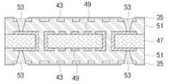
도 15는 본 발명의 또 다른 실시예에 따른 인쇄회로기판 제조방법에서 제1, 제2 및 제3금속층이 순차적으로 적층된 캐리어를 도시한 단면도.FIG. 15 is a cross-sectional view illustrating a carrier in which first, second and third metal layers are sequentially stacked in a method of manufacturing a printed circuit board according to still another embodiment of the present invention. FIG.
도 16은 도 15에서 제1금속층을 에칭하여 범프를 형성한 상태를 도시한 단면도.FIG. 16 is a cross-sectional view illustrating a state in which bumps are formed by etching the first metal layer in FIG. 15. FIG.
도 17은 도 16에서 레지스트를 박리하고 다시 레지스트를 도포한 후 외부 회로가 될 부분을 형성한 상태를 도시한 단면도.FIG. 17 is a cross-sectional view illustrating a state in which a portion to be an external circuit is formed after peeling a resist and applying a resist again in FIG. 16. FIG.
도 18은 도 17에 도금을 실시하여 외부 회로를 형성한 상태를 도시한 단면도.FIG. 18 is a cross-sectional view illustrating a state in which an external circuit is formed by plating on FIG. 17. FIG.
도 19는 도 18에서 형성된 외부 회로, 그리고 절연층 및 코어층을 순차적으로 위치시킨 상태를 도시한 단면도.19 is a cross-sectional view illustrating an external circuit formed in FIG. 18 and a state in which an insulating layer and a core layer are sequentially positioned;
도 20은 도 19에서 절연층에 내부 회로 및 외부 회로를 전사한 상태를 도시한 단면도.20 is a cross-sectional view showing a state where an internal circuit and an external circuit are transferred to an insulating layer in FIG. 19.
도 21은 도 20에서 범프를 제거한 후 도금을 실시한 상태를 도시한 단면도.21 is a cross-sectional view showing a state in which plating is performed after removing a bump in FIG. 20.
도 22는 도 21에서 비어 홀에 구리를 충진하고 도금층을 제거한 상태를 도시한 단면도.FIG. 22 is a cross-sectional view illustrating a state in which a via hole is filled with copper and a plating layer is removed in FIG. 21;
도 23은 도 22에서 캐리어의 제2금속층을 제거한 후 노광 및 현상 등을 실시하여 단자 부분을 개방한 상태를 도시한 단면도.FIG. 23 is a cross-sectional view illustrating a state in which a terminal portion is opened by exposing and developing after removing the second metal layer of the carrier in FIG. 22.
도 24는 본 발명의 다른 측면에 따른 인쇄회로기판 제조방법에서 캐리어 상에 범프를 형성한 상태를 도시한 단면도.24 is a cross-sectional view illustrating a bump formed on a carrier in a method of manufacturing a printed circuit board according to another aspect of the present invention.
도 25는 도 24에서 절연부재에 캐리어를 적층하여 범프가 캐리어 내부에 함입된 상태를 도시한 단면도.FIG. 25 is a cross-sectional view illustrating a state in which bumps are embedded in a carrier by stacking a carrier on an insulating member in FIG. 24; FIG.
도 26은 도 25에서 캐리어 및 범프를 제거한 상태를 도시한 단면도.FIG. 26 is a cross-sectional view illustrating a state in which a carrier and a bump are removed from FIG. 25. FIG.
도 27은 도 26에서 상부 회로 및 하부 회로를 형성하고 비어 홀을 이용하여 상부 회로 및 하부 회로를 전기적으로 연결한 상태를 도시하는 단면도.FIG. 27 is a cross-sectional view illustrating a state in which an upper circuit and a lower circuit are formed in FIG. 26 and an upper circuit and a lower circuit are electrically connected using a via hole; FIG.
<도면 부호의 설명><Description of Drawing>
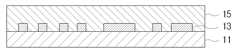
11, 47 코어층 13, 49 내부회로11, 47
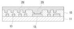
15, 51 절연층 17 외부 회로 패턴15, 51
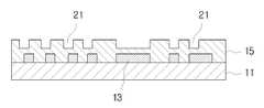
19 프레스판 21 미세홈19
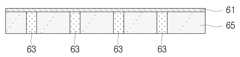
23, 53, 73 비어홀 27, 31, 61 캐리어23, 53, 73 Beer Hall 27, 31, 61 Carrier
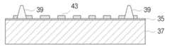
29, 43 외부회로 39, 63 범프29, 43
41, 55 레지스트 65 절연부재41, 55 resist 65 insulation member
67 관통홀 69 상부 회로67 Through Hole 69 Upper Circuit
71 하부 회로71 bottom circuit
본 발명은 인쇄회로기판 제조방법에 관한 것이다.The present invention relates to a printed circuit board manufacturing method.
최근 휴대 전화, 디지털 카메라 등의 모바일 전자기기의 경량화, 소형화, 박형화, 고성능화가 급속하게 진행되고 LSI 패키지의 고속화, 고밀도화가 요구됨에 따라 빌드 업(build up) 기판의 고밀도화가 요구되고 있다. 현재 플립 칩(flip chip) 기판은 기판의 배선 밀도를 높이기 위해 회로 형성에 SAP(Semi-Additive Process) 방식을 이용하는 것이 주류를 이루고 있다. 그러나 미세회로를 편리하게 형성하기 위해서 SAP 방식 이외의 방식에 대한 연구가 진행되고 있다.Recently, as the weight reduction, miniaturization, thinning, and high performance of mobile electronic devices such as mobile phones and digital cameras are rapidly progressing, and as the speed and density of LSI packages are required, the density of build-up substrates is required. Currently, flip chip substrates use a semi-additive process (SAP) method for circuit formation in order to increase wiring density of the substrate. However, in order to conveniently form microcircuits, studies on methods other than the SAP method are being conducted.
종래의 회로 형성 방법의 단점은 구리에 의해 형성된 회로가 절연층 상에 형성되기 때문에 절연층과 밀착된 부분이 회로의 저면(低面) 밖에 없게 된다. 따라서 미세회로를 형성하는 경우 회로와 수지의 접합 부분에 언더 컷(under cut)이 발생하여 미세 회로가 박리되는 문제점이 있다. 그리고 이와 같은 회로의 박리에 의해 기판 전체에 불량이 발생하게 된다.A disadvantage of the conventional circuit forming method is that the circuit formed by copper is formed on the insulating layer so that the portion in close contact with the insulating layer is only at the bottom of the circuit. Therefore, when the microcircuit is formed, there is a problem in that an undercut occurs in the junction between the circuit and the resin, and the microcircuit is peeled off. And defects arise in the whole board | substrate by peeling of such a circuit.
이와 같은 문제를 해결하기 위해 최근에는 임프린트(imprint) 공법 및 레이저 가공 공정에 의해 절연층에 트렌치(trench)를 형성하고 트렌치의 내부에 도체를 충진하여 회로를 형성하는 기술이 연구되고 있다.In order to solve such a problem, a technique for forming a circuit by forming a trench in an insulating layer and filling a conductor in the trench by an imprint method and a laser processing process has been recently studied.
임프린트 공법은 금형의 회로 표면에 요철(凹凸)을 형성하여 회로 패턴을 가공한 후, 이를 절연 수지에 전사함으로써 절연 수지 상에 트렌치를 형성한다. 그리고 트렌치에 도체가 되는 금속 페이스트를 충진하거나 및 금속 도금을 실시하여 트렌치에 도전성 물질을 충진함으로써 회로를 형성하게 되는 것이다. 그리고 레이저 가공 공정은 적층된 절연층의 표면에 레이저 어블레이션(laser ablation)에 의해 트렌치를 형성하고 상기 임프린트 공법과 동일한 방식으로 금속 페이스트 충진 또는 도금에 의해 회로를 형성한다.In the imprint method, irregularities are formed on a circuit surface of a mold to process a circuit pattern, and then transferred to an insulating resin to form trenches on the insulating resin. The circuit is formed by filling the trench with a metal paste serving as a conductor or by performing metal plating to fill the trench with a conductive material. In the laser processing process, the trench is formed on the surface of the laminated insulating layer by laser ablation, and the circuit is formed by metal paste filling or plating in the same manner as the imprint method.
그러나 상기 임프린트 공법은 금형이 고가이고 금형의 전사 후 금형을 절연층에서 분리하는데 많은 어려움이 있다. 또한, 금형으로 수지를 프레스하면서 경화하기 위해서는 프레스에 많은 시간이 소요되고 생산성이 떨어지는 문제점이 있다. 그리고 레이저 공법은 장비 자체가 상당히 고가일 뿐만 아니라 회로를 형성하기 위한 고가의 알루미늄 마스크 또는 유전체 마스크가 필요하다는 문제점을 갖는다.However, the imprint method is expensive and there is a lot of difficulty in separating the mold from the insulating layer after the transfer of the mold. In addition, in order to harden while pressing the resin into the mold, there is a problem that the press takes a lot of time and the productivity is low. And the laser process has the problem that the equipment itself is not only expensive but also requires an expensive aluminum mask or dielectric mask to form a circuit.
그리고 인쇄회로기판의 제조에 있어서 중요한 것이 층간 접속 방법이다.In the manufacture of printed circuit boards, the interlayer connection method is important.
층간 접속을 위해서 종래에는 기계적인 홀(hole) 가공 및 도금 방법을 이용하였으며, 기계적인 가공을 미세하고 정확하게 하는 기술과 기계 가공에 의해 형성된 홀 속에 층간 연결을 위한 도금을 얼마나 효율적으로 할 수 있는지가 문제되었다. 그리고 기술의 발전과 더불어 기계적인 홀 가공을 대신하여 레이저를 이용한 블라인드 비어 홀(blind via hole) 형태로 홀을 가공하는 기술이 계발되어 사용되고 있으며, 나아가 B2it(Buried Bump interconnection technology) 기술과 NMBI(Neo Menhatan Bump Interconnection) 기술들이 개발되어 일부는 양산되고 있다.Conventionally, mechanical hole processing and plating methods have been used for the interlayer connection, and how efficient can the plating for the interlayer connection in the holes formed by the machining and the technique of fine and precise mechanical processing are performed? It was a problem. In addition to the development of the technology, the technology of processing holes in the form of blind via holes using laser instead of mechanical hole processing has been developed and used. Menhatan Bump Interconnection) technologies have been developed and some are in production.
그러나 기계적인 홀 가공은 비트(bit)의 소모에 의해 제조 원가가 상승하고, B2it 기술은 층간 접속을 위하여 페이스트(paste)를 사용하기 때문에 반도체용 기재(substrate)로서는 이직 신뢰성이 떨어지고 홀을 미세화 하는데 한계가 있는 것으로 전해지고 있다. 또한, NMBI는 물리적으로 구리와 구리를 접속시키기 때문에 접속 신뢰성에 문제가 있다.However, in mechanical hole processing, manufacturing cost increases due to the consumption of bits, and B2it technology uses paste for interlayer connection. It is said to be limited. In addition, since NMBI physically connects copper to copper, there is a problem in connection reliability.
본 발명은 회로가 절연층에 함침되어 있기 때문에 회로의 박리가 발생하지 않으며 미세 회로를 형성할 수 있는 인쇄회로기판 제조방법을 제공하는 것을 목적으로 한다.It is an object of the present invention to provide a method for manufacturing a printed circuit board, in which a circuit is not peeled off and a fine circuit can be formed because the circuit is impregnated into an insulating layer.
본 발명은 고해상도의 회로를 형성할 수 있는 인쇄회로기판 제조방법을 제공하는 것을 목적으로 한다.An object of the present invention is to provide a printed circuit board manufacturing method capable of forming a high resolution circuit.
본 발명은 종래의 인쇄회로기판 제조공정에서 사용되는 장비를 이용하여 제조 단가를 절감 작업의 효율성을 높일 수 있는 인쇄회로기판 제조방법을 제공하는 것을 목적으로 한다.An object of the present invention is to provide a printed circuit board manufacturing method that can increase the efficiency of the work by reducing the manufacturing cost by using the equipment used in the conventional printed circuit board manufacturing process.
본 발명은 평탄도가 우수하고 열 방출이 용이한 인쇄회로기판 제조방법을 제 공하는 것을 목적으로 한다.An object of the present invention is to provide a printed circuit board manufacturing method having excellent flatness and easy heat dissipation.
본 발명은 저비용으로 층간 연결을 용이하게 할 수 있는 인쇄회로기판 제조방법을 제공하는 것을 목적으로 한다.An object of the present invention is to provide a method for manufacturing a printed circuit board which can facilitate interlayer connection at low cost.
본 발명의 일 측면에 따른 인쇄회로기판 제조방법은 내부 회로가 형성되어 있는 코어층의 적어도 일면에 절연층을 적층하고 외부 회로 패턴을 형성하는 (a) 단계, 외부 회로 패턴이 절연층에 함입되도록 하는 (b) 단계, 외부 회로 패턴을 제거하여 미세홈을 형성하고 절연층을 경화하는 (c) 단계, 미세홈에 금속을 충진하여 외부 회로를 형성하는 (d) 단계를 포함한다.According to an aspect of the present invention, there is provided a method of manufacturing a printed circuit board, by laminating an insulating layer on at least one surface of a core layer on which an internal circuit is formed and forming an external circuit pattern, such that the external circuit pattern is embedded in the insulating layer. (B) removing the external circuit pattern to form a microgroove and curing the insulating layer, and filling the metal into the microgroove to form an external circuit.
본 발명에 따른 인쇄회로기판 제조방법의 실시예들은 다음과 같은 특징들을 하나 또는 그 이상 구비할 수 있다. 예를 들면, 외부 회로와 내부 회로를 전기적으로 연결하는 (e) 단계를 더 포함할 수 있으며, 외부 회로 패턴은 절연층 상에 포토 레지스트를 리소그래피 함으로써 형성되거나 또는, 캐리어 상에 포토 레지스트를 리소그래피 함으로써 형성될 수 있다. 그리고 절연층은 열경화성 수지로 이루어지고, (b) 단계에서 절연층은 연화 상태를 유지한다. 절연층은 열가소성 수지로도 이루어질 수 있고, (b) 단계에서 절연층을 연화 온도 이상으로 가열하면서 외부 회로 패턴을 절연층에 전사한다.Embodiments of a method of manufacturing a printed circuit board according to the present invention may include one or more of the following features. For example, the method may further include (e) electrically connecting the external circuit and the internal circuit, wherein the external circuit pattern is formed by lithography of the photoresist on the insulating layer or by lithography of the photoresist on the carrier. Can be formed. The insulating layer is made of a thermosetting resin, and in step (b), the insulating layer maintains a soft state. The insulating layer may be made of a thermoplastic resin, and in step (b), the external circuit pattern is transferred to the insulating layer while the insulating layer is heated above the softening temperature.
(b) 단계에서 외부 회로 패턴은 표면이 평평한 프레스판에 의해 가압됨으로써 절연층에 전사될 수 있으며, 외부 회로 패턴은 용해 또는 팽윤에 의해 제거될 수 있다. 그리고 (d) 단계에서, 구리 도금을 이용하여 미세 홈을 충진 함으로써 외부 회로를 형성한 후 평탄화 작업을 수행할 수 있으며, (c) 단계에 있어서, 외부 회로 패턴을 제거한 후 내부 회로의 일부가 노출되도록 하는 비어 홀을 형성하고, 비어 홀의 내주면에는 도금층이 형성되어 내부 회로와 외부 회로가 전기적으로 연결될 수 있다. 또한, 외부 회로 패턴 상에는 범프가 형성되어 있고, 범프는 (b) 단계에서 전사되어 내부 회로와 접한 후 제거되어 홀을 형성하고, 홀의 내주면에는 금속층이 형성되어 내부 회로와 외부 회로가 전기적으로 연결될 수 있다.In step (b), the external circuit pattern may be transferred to the insulating layer by being pressed by a flat press plate, and the external circuit pattern may be removed by dissolution or swelling. And in step (d), by filling the fine groove using copper plating to form an external circuit can be performed after the planarization operation, in step (c), after removing the external circuit pattern, a portion of the internal circuit is exposed A via hole may be formed, and a plating layer may be formed on an inner circumferential surface of the via hole to electrically connect an internal circuit and an external circuit. In addition, bumps are formed on the external circuit pattern, and the bumps are transferred in step (b) to be removed after contact with the internal circuit to form holes, and a metal layer is formed on the inner circumferential surface of the hole to electrically connect the internal circuit and the external circuit. have.
본 발명의 다른 측면에 따른 인쇄회로기판 제조방법은 내부 회로가 형성되어 있는 코어층을 준비하는 (a) 단계, 코어층의 적어도 일면에 절연층을 개재한 상태에서 외부 회로 및 범프가 형성된 캐리어를 절연층에 가압하여 외부 회로 및 범프가 절연층에 삽입되는 (b) 단계(여기서 절연층에 삽입된 범프는 내부 회로 및 외부 회로와 접함), 그리고 캐리어 및 범프를 제거한 후 내부 회로를 외부 회로와 전기적으로 연결하는 (c) 단계를 포함한다.According to another aspect of the present invention, there is provided a method of manufacturing a printed circuit board, including (a) preparing a core layer on which an internal circuit is formed, and forming a carrier having an external circuit and a bump formed thereon with an insulating layer disposed on at least one surface of the core layer. (B) pressurizing the insulating layer to insert the external circuit and the bump into the insulating layer (where the bump inserted into the insulating layer is in contact with the internal circuit and the external circuit), and after removing the carrier and the bump, the internal circuit is connected to the external circuit. (C) electrically connecting.
인쇄회로기판 제조방법은 다음과 같은 실시예를 구비할 수 있다. 예를 들면, 범프는 상이한 3종류의 제1금속층, 제2금속층 및 제3금속층이 순차적으로 적층된 금속판에서 제1금속층을 선택적으로 제거하여 형성되고, 외부 회로는 범프와 전기적으로 연결될 수 있다. 그리고 (c) 단계에서 제2금속층의 일부를 제거하여 범프의 일부를 노출한 후 범프를 에칭에 의해 제거할 수 있다. 또한, 범프를 제거한 후 도금을 통해 그 내부를 충진함으로써 내층회로와 외층회로를 전기적으로 연결할 수도 있으며, 도금이 완료된 후 평탄화 작업을 수행할 수 있다.The printed circuit board manufacturing method may include the following embodiments. For example, the bump is formed by selectively removing the first metal layer from a metal plate in which three different kinds of first metal layers, second metal layers, and third metal layers are sequentially stacked, and an external circuit may be electrically connected to the bumps. In step (c), a part of the second metal layer may be removed to expose a part of the bump, and the bump may be removed by etching. In addition, by removing the bump and filling the inside through plating, the inner layer circuit and the outer layer circuit may be electrically connected, and after the plating is completed, the flattening operation may be performed.
본 발명의 다른 측면에 따른 인쇄회로기판 제조방법은 캐리어 상에 가용 폴리머를 이용하여 범프를 형성하는 (a) 단계, 비어를 절연부재 상에 함입한 후 캐리어를 제거하고 범프를 용융하여 관통홀을 형성하는 (b) 단계, 절연부재의 양면에 상부 회로 및 하부 회로를 형성하고 관통홀을 이용하여 상부 회로 및 하부 회로를 전기적으로 연결하는 비어홀을 형성하는 (c) 단계를 포함한다.According to another aspect of the present invention, there is provided a method of manufacturing a printed circuit board, in which (a) forming a bump using a soluble polymer on a carrier, inserting a via onto an insulating member, removing the carrier, and melting the bump to form a through hole. (B) forming, forming (c) the upper circuit and the lower circuit on both sides of the insulating member, and forming a via hole for electrically connecting the upper circuit and the lower circuit using the through hole.
여기서, 범프는 수용성 폴리머에 의해 형성되고, (b) 단계에서 범프는 수세에 의해 제거될 수 있다.Here, the bumps are formed by water-soluble polymers, and in step (b) the bumps can be removed by washing with water.
이하, 본 발명에 따른 인쇄회로기판 제조방법의 실시 예를 첨부 도면을 참조하여 상세히 설명하기로 하며, 첨부 도면을 참조하여 설명함에 있어, 동일하거나 대응하는 구성 요소는 동일한 도면번호를 부여하고 이에 대한 중복되는 설명은 생략하기로 한다.Hereinafter, an embodiment of a printed circuit board manufacturing method according to the present invention will be described in detail with reference to the accompanying drawings, in the description with reference to the accompanying drawings, the same or corresponding components are given the same reference numerals and Duplicate explanations will be omitted.
도 1은 본 발명의 일 실시예에 따른 인쇄회로기판의 제조방법을 실시하기 위해 사용되는 코어층을 도시한 단면도이다.1 is a cross-sectional view showing a core layer used to implement a method of manufacturing a printed circuit board according to an embodiment of the present invention.
도 1을 참조하면, 코어층(11)의 양면에는 내부 회로(13)가 형성되어 있다. 도 1에서는 코어층(11)의 양면에 내부 회로(13)가 형성되어 있지만, 그 일면에만 내부 회로가 형성될 수 있다. 그리고 내부 회로(13)는 추후 공정에 의해 절연층 사이에 매몰되기 때문에 종래의 미세 회로에서 발생하는 언더 컷이 발생하지 않는다. 또한 내부 회로(13)는 추후 공정에 의해 형성되는 비어 홀에 의해 외부 회로와 전기적으로 연결된다.Referring to FIG. 1,
도 2는 도 1의 코어층(11)의 일면에 절연층(15)을 적층한 상태를 도시한 단면도이다.2 is a cross-sectional view illustrating a state in which the insulating
절연층(15)은 열경화성 수지로 이루어지며, 절연층(15)을 연화 온도까지 가열하여 코어층(11)의 적어도 일면에 적층한다. 물론, 필요에 따라서 코어층(11)의 양면에 절연층(15)을 적층할 수도 있다. 일반적으로 적층되는 열경화성 수지는 약 180℃에서 경화가 개시되기 때문에 열경화성 수지로 이루어진 절연층(15)을 적층할 때에는 약 100℃ 정도를 유지하면서 가열하고, 적층이 완료된 후에도 절연층(15)을 미경화 상태로 둔다. 이는 추후 절연층(15)에 외부 회로 패턴이 전사될 수 있도록 하기 위함이다.The insulating
절연층(15)은 하나 이상의 열경화성 수지를 혼합한 조성물로 이루어질 수 있다. 열경화성 수지 조성물은 에폭시 수지, 시안산 에스테르 수지, 비스말레이미드 수지, 폴리이미드수지, 관능기 함유 폴리페니렌 에테르 수지 등의 수지가 단독 또는 2종 이상 배합된 조성으로 이루어진다.The insulating
열경화성 수지 조성물에는 다양한 첨가물을 첨가할 수 있다. 예를 들어, 열가역성 수지, 유기 충전제, 무기 충전제, 염료, 안료, 증점제, 활제, 소포제, 분산제, 레벨링제, 광택제, 중합 개시제, 칙소성 부여제 등 각종 첨가제가 목적 및 용도에 따라서 첨가된다. 또한, 난연제도 인, 브롬으로 난연화된 것, 비할로겐(non-halogen) 타입의 난연제를 사용할 수 있으며, 난연화되어 있지 않은 것도 사용 가능하다.Various additives can be added to a thermosetting resin composition. For example, various additives, such as a thermoreversible resin, an organic filler, an inorganic filler, a dye, a pigment, a thickener, a lubricant, an antifoaming agent, a dispersing agent, a leveling agent, a brightening agent, a polymerization initiator, a thixotropic imparting agent, are added according to the purpose and use. In addition, a flame retardant, flame retardant with bromine, non-halogen (non-halogen) type of flame retardant may be used, and non-flame retardant may be used.
열경화성 수지 조성물은 그 자체를 가열함으로써 경화되지만, 경화속도를 높 여서 생산성을 향상시키기 위해 상기 열경화성 수지 조성물에 경화제 또는 열경화 촉매를 첨가할 수 있다.The thermosetting resin composition is cured by heating itself, but a curing agent or a thermosetting catalyst may be added to the thermosetting resin composition in order to increase the curing rate and improve productivity.
도 3은 도 2에서 절연층(15) 상에 외부 회로 패턴(17)을 도시한 단면도이다.3 is a cross-sectional view illustrating the
도 3을 참조하면, 절연층(15) 상에 감광성 포토 레지스트(photo resist)를 도포한 후 적층하고 노광 및 현상에 의해 외부 회로 패턴(17)을 형성한다. 이때 절연층(15)은 미경화된 상태에 있다. 외부 회로 패턴(17)은 추후 공정에서 형성하고자 하는 외부 회로와 동일한 패턴을 갖고, 추후에 설명하는 공정에 의해 제거되어 외부 회로에 대응하는 홈을 형성한다. 외부 회로 패턴(17)을 제조하는 과정에서 내부 회로(13)에 대한 외부 회로 패턴(17)의 위치가 중요하다. 따라서 외부 회로 패턴(17)을 형성할 때 내부 회로(13)에서 기준 위치를 정한 다음 백 라이트(back light)를 이용하여 외부 회로 패턴(17)과 내부회로(13)의 상대적 위치를 관찰하면서 외부 회로 패턴(17)의 위치를 정밀하게 조정한다.Referring to FIG. 3, a photosensitive photo resist is coated on the insulating
도 4는 도 3에서 프레스판(19)을 이용하여 외부 회로 패턴(17)을 절연층(15)에 전사한 상태를 도시한 단면도이다.FIG. 4 is a cross-sectional view illustrating a state in which the
도 4를 참조하면, 진공 상태에서 절연층(15)을 연화 온도 이상으로 가열하면서 표면이 평평한 스텐레스 판(stainless plate)과 같은 프레스판(19)을 이용하여 가압하여 외부 회로 패턴(17)이 절연층(15) 내부에 매몰되도록 한다. 이로 인해 외부 회로 패턴(17)은 그 일면만이 외부로 노출되고 나머지 면은 절연층(15)에 의해 둘러 싸여 있다. 그 후 프레스판(19)을 제거한다.Referring to FIG. 4, the
본 실시예에 따른 인쇄회로기판 제조방법에서는 표면이 평평한 프레스판에 의해 가압되기 때문에 그 압력이 절연층(15)에 균등하게 전달됨으로써 기판 전체의 휨이나 뒤틀림을 방지할 수 있다. 그리고 진공 상태에서 가압되기 때문에 절연층(15) 등에 기포 등이 발생하지 않게 된다.In the method of manufacturing a printed circuit board according to the present embodiment, since the surface is pressed by a flat press plate, the pressure is evenly transmitted to the insulating
도 5는 도 4에서 외부 회로 패턴(17)을 제거한 상태를 도시한 단면도이다.FIG. 5 is a cross-sectional view illustrating a state in which the
도 5를 참조하면, 절연층(15)에 매몰된 외부 회로 패턴(17)을 용해 또는 팽윤 박리에 의해 제거한다. 통상적으로 감광성 포토 레지스트의 박리에는 수산화 나트륨 용액이 사용되지만, 가열에 의해 박리가 곤란한 경우에는 아민계 박리제 또는 용재를 사용할 수도 있다. 외부 회로 패턴(17)이 제거되면 외부 회로에 해당하는 미세홈(21)이 형성된다.Referring to FIG. 5, the
도 6은 도 5에서 내부 회로(13)의 일부를 노출하는 비어 홀(23)을 형성한 상태를 도시한 단면도이다.FIG. 6 is a cross-sectional view illustrating a state in which the via
도 6을 참조하면, 레이저 드릴 또는 CNC(Computer Numerical Control) 드릴을 이용하여 코어층(11)의 내부 회로(13)와 접속하기 위한 비어 홀(23)을 형성한다. CNC 드릴을 이용한 경우 디스미어(desmear) 공정 및 디버(deburring) 공정을 추가로 수행할 수 있다. 물론, 내부 회로(13)와 추후 공정에 의해 형성될 외부 회로의 접속이 필요 없는 경우 비어 홀(23)을 형성하지 않아도 된다. 비어 홀(23)을 형성한 후 열경화성 수지로 이루어지는 절연층(15)을 경화한다.Referring to FIG. 6, a via
도 7은 도 6에서 미세 홈(21) 및 비어 홀(23)에 도금을 수행한 상태를 도시한 단면도이고, 도 8은 도 7에서 도금층의 일부를 제거하여 기판의 표면을 평활하게 한 상태를 도시한 단면도이다.FIG. 7 is a cross-sectional view illustrating a state in which the
도 7 및 도 8을 참조하면, 구리 도금을 수행하여 미세 홈(21)을 충진하여 외부 회로(29)를 형성한다. 외부 회로(29)는 그 자체가 외부로 노출되어 저항, 커패시터(capacitor) 등과 같은 수동 소자 또는 IC 등과 같은 능동 소자와 전기적으로 연결될 수 있다. 그리고 외부 회로(29) 상에 또 다른 회로층이 적층될 수도 있다. 또한, 외부 회로(29)는 비어 홀(23)에 충전된 구리 도금에 의해 내부 회로(13)와 전기적으로 연결된다. 도금 공정을 수행한 후 기판의 표면을 매끄럽게 하기 위해서 평탄화(planarization) 작업을 수행한다.Referring to FIGS. 7 and 8, copper plating is performed to fill the
절연층(15)이 열가소성 수지로 이루어진 경우에는, 상기 도 2에서와 같이 절연층(15)을 코어층(11)의 적어도 일면에 적층한 후 감광성 포토 레지스트를 이용하여 노광 및 현상 등에 의해 외부 회로 패턴(17)을 형성한다. 그리고 절연층(15)을 열가소성 수지의 연화 온도 이상으로 가열하면서 외부 회로 패턴(17)을 프레스판을 이용하여 절연층(15)의 내부에 전사한다. 그리고 위에서 설명한 바와 같이 외부 회로 패턴(17)을 제거한 후 절연층을 경화하고 비어 홀(23)을 형성한 후 구리 도금 및 평탄화 작업을 실시하여 기판을 완성한다.When the insulating
이하에서는 본 발명의 다른 실시예에 따른 인쇄회로기판 제조방법에 대해서 도 9 내지 도 14를 참조하면서 설명하기로 한다.Hereinafter, a method of manufacturing a printed circuit board according to another exemplary embodiment of the present invention will be described with reference to FIGS. 9 to 14.
도 9는 내부 회로(13)가 형성된 코어층(11), 미경화 상태에 있는 절연층(15), 그리고 외부 회로 패턴(17)이 형성된 캐리어(27)를 순차적으로 위치시킨 상태를 도시한 단면도이다.FIG. 9 is a cross-sectional view illustrating a state in which the
도 9를 참조하면, 캐리어(27)의 일면에는 감광성 포토 레지스트에 의해 형성 된 외부 회로 패턴(17)이 형성되어 있다. 외부 회로 패턴(17)은 앞서 실시예에서 절연층(15)의 상부에 형성된 외부 회로 패턴에 대응하는 것으로, 추후 공정에서 전사되어 절연층(15)의 내부에 매몰된다. 그리고 절연층(15)은 미경화 상태에 있는 열경화성 수지 또는 열가소성 수지를 사용하고, 코어층(11)의 일면에는 내부 회로(13)가 형성되어 있다.Referring to FIG. 9, an
도 10은 도 9에서 캐리어(27)를 가압하여 코어층(11)에 절연층(15)이 적층되고 절연층(15)에 외부 회로 패턴(17)이 전사된 상태를 도시한 단면도이다.FIG. 10 is a cross-sectional view illustrating a state in which the insulating
도 10을 참조하면, 캐리어(27)를 열 압착에 의해 가압하여 미경화 상태에 있는 절연층(15)이 코어층(11) 상에 적층됨과 동시에 캐리어(27)의 일면에 형성된 외부 회로 패턴(17)이 절연층(15)의 내부에 전사되도록 한다. 이때 절연층(15)은 연화 온도 이상으로 가열한다. 그리고 내부 회로(13)에 대한 외부 회로 패턴(17)의 위치를 정밀하게 유지하기 위해서, 백 라이트 등을 이용하여 내부 회로(13)와 외부 회로 패턴(17) 상대적 위치 관계를 관찰하면서 적층 및 전사를 수행한다.Referring to FIG. 10, an external circuit pattern formed on one surface of the
도 11은 도 10에서 캐리어(27) 및 외부 회로 패턴(17)을 제거한 상태를 도시한 단면도이고, 도 12는 도 11에서 비어 홀(23)을 형성한 상태를 도시한 단면도이다.FIG. 11 is a cross-sectional view illustrating a state in which the
도 11을 참조하면, 위에서 설명한 바와 같이, 감광성 포토 레지스트로 형성된 외부 회로 패턴(17)을 용제를 이용하여 녹이거나 팽윤 공정 등을 이용하여 제거한다. 외부 회로 패턴(17)이 제거된 곳에는 미세 홈(21)이 형성된다. 그리고 도 12를 참조하면, 내부 회로(13)의 일부가 노출되도록 비어 홀(23)을 형성한다. 비어 홀(23)의 형성 방법은, 위에서 설명한 바와 같이, 레이저 드릴 또는 CNC 드릴 등을 이용한다.Referring to FIG. 11, as described above, the
도 13은 도 12에서 형성된 미세 홈(21)에 구리 도금을 실시한 상태를 도시한 단면도이고, 도 14는 도 13에서 평탄화 작업을 수행한 단면도이다.FIG. 13 is a cross-sectional view showing a state in which copper plating is performed on the
도 13을 참조하면, 구리 도금을 이용하여 미세 홈(21)을 충진함으로써 외부 회로(29)를 형성한다. 이때, 비어 홀(23)도 함께 충진되어서 외부 회로(29) 및 내부 회로(13)가 전기적으로 연결된다. 그리고 도 14에서와 같이 평탄화 작업이 수행되어 구리 도금의 일부가 제거되어 외부 회로(29)는 그 일 면만이 외부로 노출되고 다른 면은 절연층(15)과 접한다.Referring to FIG. 13, the
이와 같이 본 실시 예들에 따른 인쇄회로기판 제조방법에 의해 제조된 인쇄회로기판은 미세한 회로가 절연층의 내부에 매몰되어 있기 때문에 언더 컷 등에 의해 회로의 박리가 발생하지 않는다. 그리고 고해상도를 가지는 감광성 포토 레지스트를 이용하여 회로를 형성하기 때문에, 레지스트의 해상도가 외부 회로의 해상도가 되어 미세한 회로를 형성하는 것이 용이하다. 또한, 감광성 포토 레지스트를 리소그래피 공법에 의해 외부 회로 패턴을 이용하고 이를 전사한 후 비어 홀 형성 및 구리 도금 등을 실시하는데, 이는 종래의 인쇄회로기판의 공정을 그대로 사용하는 것으로 새로운 장비를 도입할 필요가 없다. 따라서 본 실시예에 따른 인쇄회로기판 제조방법은 제조 비용이 저렴하고 생산성이 우수한 효과를 도모할 수 있다.As described above, in the printed circuit board manufactured by the method of manufacturing the printed circuit board according to the exemplary embodiments, since the fine circuit is buried in the insulating layer, the circuit is not peeled off due to the undercut. And since a circuit is formed using the photosensitive photoresist which has high resolution, it is easy to form a fine circuit by making the resolution of a resist into the resolution of an external circuit. In addition, the photosensitive photoresist uses an external circuit pattern by a lithography method, transfers it, and then forms via holes, copper plating, etc., which uses a conventional printed circuit board process as it is, and needs to introduce new equipment. There is no. Therefore, the printed circuit board manufacturing method according to the present embodiment can achieve the effect of low manufacturing cost and excellent productivity.
이하에서는, 도 15 내지 도 23을 참조하면서 본 발명의 다른 실시예에 따른 인쇄회로기판의 제조방법에 대해서 설명하기로 한다.Hereinafter, a method of manufacturing a printed circuit board according to another exemplary embodiment of the present invention will be described with reference to FIGS. 15 to 23.
도 15는 외부 회로 및 범프가 형성되는 캐리어(31)를 도시한 단면도이다.15 is a cross-sectional view showing a carrier 31 in which external circuits and bumps are formed.
도 15를 참조하면, 알루미늄으로 형성된 제1금속층(33), 니켈로 형성된 제2금속층(35), 그리고 구리로 이루어진 제3금속층(37)이 순차적으로 적층되어 있다. 각각의 금속층(33, 35, 37)은 금속 결합 또는 유기물 등에 의해 상호 결합되어 있다. 제1금속층 내지 제3금속층(33, 35, 37)은 상기 금속 이외의 다른 금속으로 형성될 수 있음은 물론이다. 제1금속층(33)은 추후 공정에 의해 제거되어 범프가 형성된다. 범프는 외부 회로와 내부 회로를 전기적으로 연결하는 역할을 하기 때문에, 제1금속층(33)의 높이를 조절하여 범프가 외부 회로에서 내부 회로와 접할 수 있도록 하는 것이 바람직하다. 그리고 하나의 금속층을 에칭에 의해 제거하는 경우 다른 금속층은 그 에칭 용액에 의해 제거되지 않도록 금속층을 형성하는 것이 바람직하다.Referring to FIG. 15, a
도 16은 도 15에서 에칭 공정에 의해 제1금속층(33)의 일부를 제거하여 범프(39)를 형성한 상태를 도시한 단면도이다.FIG. 16 is a cross-sectional view illustrating a state in which a
도 15에서 제1금속층(33) 상에 감광성 포토 레지스트(41)를 도포한 후 노광 및 현상을 수행하여 제1금속층(33)을 에칭하면, 도 16에서와 같이 범프(39)가 형성된다. 범프(39)는 추후 공정에 의해 형성되는 외부 회로와 전기적으로 연결되기 때문에 범프의 높이 뿐만 아니라 범프(39)의 위치를 정확하게 형성하는 것도 중요하다.In FIG. 15, after the
도 17은 도 16에서 레지스트(41)를 박리하고 다시 레지스트(42)를 도포한 후 노광 및 현상을 진행하여 외부 회로가 형성될 부분을 제조한 단면도이고, 도 18은 도 17에서 구리 도금을 수행한 상태를 도시한 단면도이다.FIG. 17 is a cross-sectional view illustrating a part in which an external circuit is formed by exposing the resist 41 and applying the resist 42 again after exposure and development in FIG. 16, and FIG. 18 is performed to perform copper plating in FIG. 17. It is sectional drawing which shows one state.
도 17을 참조하면, 범프(39)의 상부에 위치한 레지스트(41)를 박리하여 제거한 후 다시 범프(39) 이외의 부분에 감광성 포토 레지스트(42)를 도포한 후 외층 회로가 형성될 부분을 노광 및 현상을 이용하여 제거한다. 그리고 도 18에 도시된 바와 같이, 전기 동도금을 이용하여 상기 레지스트(42)가 제거된 부분에 구리가 충진되어 외부 회로(43)가 형성된다. 그리고 도 17과 같이 형성된 포토 레지스트를 제거한다. 도면에는 도시하지 않았지만, 범프(39)의 외주면에도 도금층이 형성될 수 있다.Referring to FIG. 17, after removing and removing the resist 41 positioned on the
도 19는 도 18에서 형성된 외부 회로(43) 및 범프(39)를 절연층(51)을 개재한 상태에서 코어층(47)의 양면에 적층하는 상태를 도시한 단면도이고, 도 20은 도 19에 도시된 각각의 층을 적층한 결과를 도시한 단면도이다.FIG. 19 is a cross-sectional view illustrating a state in which the
도 19를 참조하면, 코어층(47)은 그 양면에 형성된 내부 회로(49)를 구비한다. 내부 회로(49)는 절연층의 양면에 형성되어 도통 홀(50)에 의해 전기적으로 연결되어 있다. 코어층(47)의 양면에 절연층(51)을 각각 개재한 상태에서 외부 회로(43) 및 범프(39)를 고온 및 고압의 조건에서 전사한다. 그 결과, 도 20에서와 같이 코어층(47)의 내부 회로(49), 외부 회로(43) 및 범프(39)가 절연층(51)의 내부에 매몰된다. 그리고 전사 과정이 완료되면 구리에 의해 형성된 제3금속층(37)을 제거한다. 제3금속층(37)이 금속 결합에 의해 제2금속층(35)에 결합된 경우 에칭을 이용하고, 유기물에 의해 결합된 경우 제3금속층(37)을 박리하여 제거한다.Referring to FIG. 19, the
도 21은 도 20에서 범프(39)를 제거한 후 도금을 실시한 상태를 도시한 단면 도이고, 도 22는 도 21에서 비어 홀에 구리를 충진하고 도금층을 제거한 상태를 도시한 단면도이다.FIG. 21 is a cross-sectional view illustrating a state in which plating is performed after removing the
도 21을 참조하면, 범프(39)가 형성된 부분의 제2금속층(35)을 에칭 또는 레이저 가공에 의해 범프(39)의 크기에 비해 더 크게 제거한다. 이로 인해 외부 회로(43)의 일부 및 이와 전기적으로 연결된 범프(39)의 일부가 외부로 노출된다. 제2금속층(35)을 제거한 후 범프(39)를 에칭으로 제거하여 비어 홀(53) 형상을 구현한다. 범프(39)는 알루미늄으로 이루어져 있는데, 알루미늄 범프의 에칭에 의해 제2금속층(35)은 제거되지 않는다. 그리고 도 21에 도시된 바와 같이, 비어 홀(53) 부분에 도금을 하기 위해 화학 동을 이용하여 구리 층을 얇게 형성한다. 그 후, 도 22에 도시된 바와 같이, 레지스트를 도포하여 노광 및 현상에 의해 비어 홀(53) 부분만 개방한 후 전기 도금을 이용하여 비어 홀(53)을 구리를 이용하여 충진한다. 그리고 기판의 평탄도를 맞추기 위해서 비어 홀 위로 돌출된 구리를 약한 에칭으로 일정량 제거한 후, 도 22와 같이 레지스트 및 도금 부분의 일정량을 제거한다.Referring to FIG. 21, the
그 후, 도 23에 도시된 바와 같이, 제2금속층(35)을 에칭하여 제거한 후 솔더 레지스트(57)를 도포한 후 노광 및 현상을 실시하여 전자 부품을 실장할 부분을 개방하고 필요한 전처리를 통해서 제품 제조를 완료한다.After that, as shown in FIG. 23, the
이상에서 살펴 본 인쇄회로기판의 제조방법은 회로가 수지에 함침되기 때문에 회로가 박리되는 문제점을 해결할 수 있다. 그리고 도 22에 도시된 제2금속층(35)을 제거하기 때문에 도금에 의해 공정을 마무리하는 종래의 인쇄회로기판 제조방법에 비해 기판의 평탄도가 우수하며, 비어 홀을 별도로 가공할 필요가 없기 때문에 제조 비용을 줄일 수 있을 뿐만 아니라 비어 홀에 구리가 충진되어 있기 때문에 열의 방출이 용이한 장점을 가진다.The manufacturing method of the printed circuit board described above can solve the problem of the circuit peeling because the circuit is impregnated in the resin. In addition, since the
이하에서는 본 발명의 다른 측면에 따른 인쇄회로기판 제조방법에 대해서 설명하기로 한다.Hereinafter, a method of manufacturing a printed circuit board according to another aspect of the present invention will be described.
도 24를 참조하면, 캐리어(61) 상에 복수 개의 범프(63)가 형성되어 있음을 알 수 있다. 범프(63)는 가용성 폴리머(soluble polymer)에 의해 형성되며, 특히 수용성 폴리머에 의해 형성될 수 있다. 수용성 폴리머를 이용하여 범프(63)를 형성함으로써 범프(63)를 수세(水洗)에 의해 용이하게 제거할 수 있다. 범프((63)의 높이는 아래에서 설명하는 바와 같이 절연부재(65)의 두께와 거의 동일하게 형성될 수 있다.Referring to FIG. 24, it can be seen that a plurality of
범프(63)를 형성하는 방법으로는 인쇄회로기판의 제조에 일반적으로 사용되는 프린팅(printing) 방법이 사용되고, 제품의 조건에 따라서 잉크젯 또는 포토 리소그래피 등의 방법이 사용될 수 있다. 그리고 캐리어(61)로는 일정한 두께와 강도를 갖고 있는 동박 등을 사용할 수 있다.As a method of forming the
도 25를 참조하면, 상기 캐리어(61)를 절연부재(65) 상에 적층하여 범프(63)가 절연부재(65)의 내부에 함입되어 있음을 알 수 있다. 범프(63)의 길이는 절연부재(65)의 두께와 동일하거나 실질적으로 동일하기 때문에 범프(63)의 일단부가 절연부재(65)의 일면에서 거의 노출될 수 있다.Referring to FIG. 25, it can be seen that the
그리고, 도 26에 도시된 바와 같이, 캐리어(61)를 제거한 후 수세 등을 이용하여 범프(63)도 제거한다. 범프(63)의 제거에 의해 절연부재(65)의 상면 및 하면 을 관통하는 관통홀(67)이 형성된다. 그리고 절연부재(65)의 상면 및 하면에 회로를 형성하기 위해서 절연부재(65)의 표면에 표면처리를 선택적으로 실시한다. 그 후, 도 27에 도시된 바와 같이 상부 회로(69) 및 하부 회로(71)를 절연부재(65)의 상면 및 하면에 각각 형성한 후 관통홀(67)의 내부에 전기 도금을 실시하여 상부 회로(69) 및 하부 회로(71)를 전기적으로 연결한다.And, as shown in FIG. 26, after removing the
본 실시 예에 따른 인쇄회로기판 제조방법에 있어서, 층간 접속을 위해서 기계적인 홀 가공 등을 실시하지 않기 때문에, 제조비용 및 시간을 절감할 수 있다.In the method of manufacturing a printed circuit board according to the present embodiment, mechanical hole processing or the like is not performed for interlayer connection, thereby reducing manufacturing cost and time.
이상에서 본 발명의 실시 예를 설명하였지만, 본 발명의 다양한 변경 예와 수정 예도 본 발명의 기술적 사상을 구현하는 한 본 발명의 범위에 속하는 것으로 해석되어야 한다.Although the embodiments of the present invention have been described above, various changes and modifications of the present invention should also be construed as falling within the scope of the present invention as long as the technical idea of the present invention is implemented.
본 발명은 회로가 절연층에 함침되어 있기 때문에 회로의 박리가 발생하지 않으며 미세 회로를 형성할 수 있는 인쇄회로기판 제조방법을 제공할 수 있다.The present invention can provide a method of manufacturing a printed circuit board which can form a fine circuit without causing circuit peeling because the circuit is impregnated into the insulating layer.
본 발명은 고해상도의 회로를 형성할 수 있는 인쇄회로기판 제조방법을 제공할 수 있다.The present invention can provide a printed circuit board manufacturing method capable of forming a high resolution circuit.
본 발명은 종래의 인쇄회로기판 제조공정에서 사용되는 장비를 이용하여 제조 단가를 절감 작업의 효율성을 높일 수 있는 인쇄회로기판 제조방법을 제공할 수 있다.The present invention can provide a printed circuit board manufacturing method that can reduce the manufacturing cost by using the equipment used in the conventional printed circuit board manufacturing process to increase the efficiency of the work.
본 발명은 평탄도가 우수하고 열 방출이 용이한 인쇄회로기판 제조방법을 제공할 수 있다.The present invention can provide a printed circuit board manufacturing method having excellent flatness and easy heat dissipation.
본 발명은 저비용으로 층간 연결을 용이하게 할 수 있는 인쇄회로기판 제조방법을 제공할 수 있다.The present invention can provide a printed circuit board manufacturing method that can facilitate the interlayer connection at low cost.
Claims (18)
Translated fromKoreanPriority Applications (2)
| Application Number | Priority Date | Filing Date | Title |
|---|---|---|---|
| KR1020060085789AKR100761706B1 (en) | 2006-09-06 | 2006-09-06 | Printed Circuit Board Manufacturing Method |
| US11/896,774US8065797B2 (en) | 2006-09-06 | 2007-09-05 | Fabricating method for printed circuit board |
Applications Claiming Priority (1)
| Application Number | Priority Date | Filing Date | Title |
|---|---|---|---|
| KR1020060085789AKR100761706B1 (en) | 2006-09-06 | 2006-09-06 | Printed Circuit Board Manufacturing Method |
Publications (1)
| Publication Number | Publication Date |
|---|---|
| KR100761706B1true KR100761706B1 (en) | 2007-09-28 |
Family
ID=38738691
Family Applications (1)
| Application Number | Title | Priority Date | Filing Date |
|---|---|---|---|
| KR1020060085789AExpired - Fee RelatedKR100761706B1 (en) | 2006-09-06 | 2006-09-06 | Printed Circuit Board Manufacturing Method |
Country Status (2)
| Country | Link |
|---|---|
| US (1) | US8065797B2 (en) |
| KR (1) | KR100761706B1 (en) |
Cited By (9)
| Publication number | Priority date | Publication date | Assignee | Title |
|---|---|---|---|---|
| KR100897316B1 (en)* | 2007-10-26 | 2009-05-14 | 삼성전기주식회사 | Manufacturing method of printed circuit board |
| KR100910794B1 (en)* | 2007-11-22 | 2009-08-04 | 삼성전기주식회사 | Manufacturing method of printed circuit board |
| KR100936078B1 (en) | 2007-11-12 | 2010-01-12 | 삼성전기주식회사 | Electrical member and manufacturing method of printed circuit board using the same |
| KR100940169B1 (en)* | 2008-03-07 | 2010-02-03 | 삼성전기주식회사 | Manufacturing Method of Printed Circuit Board Forming Cured Resin Layer |
| KR100966336B1 (en)* | 2008-04-07 | 2010-06-28 | 삼성전기주식회사 | High Density Circuit Board and Formation Method |
| KR100999506B1 (en)* | 2008-09-09 | 2010-12-09 | 삼성전기주식회사 | Printed Circuit Board and Manufacturing Method Thereof |
| KR101021069B1 (en) | 2008-12-23 | 2011-03-11 | 안복만 | Method of forming double-sided electronic circuit with aluminum heat dissipation structure |
| KR101078665B1 (en) | 2010-04-01 | 2011-11-01 | 주식회사 심텍 | Ultra thin PCB and manufacturing method for the same |
| CN115151026A (en)* | 2022-07-30 | 2022-10-04 | 乐健科技(珠海)有限公司 | Preparation method of circuit board with built-in electrical insulating heat sink |
Families Citing this family (23)
| Publication number | Priority date | Publication date | Assignee | Title |
|---|---|---|---|---|
| KR100841987B1 (en)* | 2007-07-10 | 2008-06-27 | 삼성전기주식회사 | Multi-layer printed circuit board manufacturing method |
| KR100894178B1 (en)* | 2007-09-28 | 2009-04-22 | 삼성전기주식회사 | Printed Circuit Board Manufacturing Method |
| KR101077380B1 (en)* | 2009-07-31 | 2011-10-26 | 삼성전기주식회사 | A printed circuit board and a fabricating method the same |
| KR20110037332A (en)* | 2009-10-06 | 2011-04-13 | 삼성전기주식회사 | Printed circuit board and manufacturing method thereof |
| KR101109230B1 (en)* | 2009-10-20 | 2012-01-30 | 삼성전기주식회사 | Printed circuit board and manufacturing method thereof |
| TWI399136B (en)* | 2009-11-17 | 2013-06-11 | Unimicron Technology Corp | Circuit board and manufacturing method thereof |
| KR101203965B1 (en)* | 2009-11-25 | 2012-11-26 | 엘지이노텍 주식회사 | Printed circuit board and manufacturing method of the same |
| TWI405515B (en)* | 2009-12-30 | 2013-08-11 | Unimicron Technology Corp | Circuit board and manufacturing method thereof |
| KR101181048B1 (en)* | 2010-12-27 | 2012-09-07 | 엘지이노텍 주식회사 | The method for manufacturing the printed circuit board |
| KR101926560B1 (en)* | 2011-12-15 | 2018-12-10 | 엘지이노텍 주식회사 | The printed circuit board and the method for manufacturing the same |
| US9000302B2 (en)* | 2013-04-17 | 2015-04-07 | Shinko Electric Industries Co., Ltd. | Wiring board |
| KR101516072B1 (en)* | 2013-07-09 | 2015-04-29 | 삼성전기주식회사 | Semiconductor Package and Method of Manufacturing The Same |
| TWI576025B (en) | 2014-10-29 | 2017-03-21 | 矽品精密工業股份有限公司 | Substrate structure and fabrication method thereof |
| CN106658977B (en)* | 2015-10-29 | 2019-11-12 | 碁鼎科技秦皇岛有限公司 | The circuit manufacturing method of circuit board and the circuit board made using this method |
| US10983647B2 (en)* | 2017-08-10 | 2021-04-20 | Sharp Kabushiki Kaisha | Method for manufacturing circuit board |
| TWI661759B (en)* | 2018-07-19 | 2019-06-01 | 欣興電子股份有限公司 | Substrate structure and manufacturing method thereof |
| CN114745862B (en)* | 2021-01-07 | 2024-12-17 | 欣兴电子股份有限公司 | Circuit board and manufacturing method thereof |
| TWI740767B (en)* | 2021-01-07 | 2021-09-21 | 欣興電子股份有限公司 | Circuit board and manufacturing method of the circuit board |
| JPWO2022202552A1 (en)* | 2021-03-22 | 2022-09-29 | ||
| WO2022202547A1 (en)* | 2021-03-22 | 2022-09-29 | パナソニックIpマネジメント株式会社 | Wiring body, mounting substrate, method for manufacturing wiring body, and method for manufacturing mounting substrate |
| EP4319510A4 (en)* | 2021-03-22 | 2024-10-02 | Panasonic Intellectual Property Management Co., Ltd. | WIRING BODY, MOUNTING SUBSTRATE, WIRING TRANSFER BOARD WITH WIRING, INTERMEDIATE MATERIAL FOR A WIRING BODY AND MANUFACTURING METHOD FOR A WIRING BODY |
| JP2023010236A (en)* | 2021-07-09 | 2023-01-20 | イビデン株式会社 | Wiring board and method for manufacturing wiring board |
| CN115884494A (en)* | 2021-09-28 | 2023-03-31 | 深南电路股份有限公司 | A method for embedding lines and PCB boards for embedding lines |
Citations (5)
| Publication number | Priority date | Publication date | Assignee | Title |
|---|---|---|---|---|
| WO1995012386A1 (en)* | 1993-11-04 | 1995-05-11 | Schering Aktiengesellschaft | Charged liposome preparation |
| JP2002076621A (en) | 2000-08-31 | 2002-03-15 | Elna Co Ltd | Multilayer circuit board and its manufacturing method |
| JP2002094233A (en) | 2000-09-18 | 2002-03-29 | Matsushita Electric Ind Co Ltd | Circuit board manufacturing method |
| JP2002100851A (en) | 2000-09-21 | 2002-04-05 | Cmk Corp | Manufacturing method of printed wiring board |
| KR20060019964A (en) | 2004-08-30 | 2006-03-06 | 엘지전자 주식회사 | Manufacturing method of printed circuit board |
Family Cites Families (24)
| Publication number | Priority date | Publication date | Assignee | Title |
|---|---|---|---|---|
| CA2059020C (en)* | 1991-01-09 | 1998-08-18 | Kohji Kimbara | Polyimide multilayer wiring board and method of producing same |
| EP0647090B1 (en)* | 1993-09-03 | 1999-06-23 | Kabushiki Kaisha Toshiba | Printed wiring board and a method of manufacturing such printed wiring boards |
| JP2736042B2 (en)* | 1995-12-12 | 1998-04-02 | 山一電機株式会社 | Circuit board |
| US6085414A (en)* | 1996-08-15 | 2000-07-11 | Packard Hughes Interconnect Company | Method of making a flexible circuit with raised features protruding from two surfaces and products therefrom |
| JP2934202B2 (en)* | 1997-03-06 | 1999-08-16 | 山一電機株式会社 | Method for forming conductive bumps on wiring board |
| DE59915155D1 (en)* | 1998-08-28 | 2010-05-27 | Dyconex Ag | PROCESS FOR MICRO-OXYGEN GENERATION |
| KR100333627B1 (en)* | 2000-04-11 | 2002-04-22 | 구자홍 | Multi layer PCB and making method the same |
| JP2002090388A (en)* | 2000-09-13 | 2002-03-27 | Soushiyou Tec:Kk | Lead contact structure |
| JP3890901B2 (en)* | 2001-02-21 | 2007-03-07 | ソニー株式会社 | Electronic component mounting substrate and manufacturing method thereof |
| JP2003188338A (en)* | 2001-12-13 | 2003-07-04 | Sony Corp | Circuit board and its manufacturing method |
| JP2003318545A (en)* | 2002-04-22 | 2003-11-07 | Sony Corp | Multilayer printed wiring board and its manufacturing method |
| WO2004034759A1 (en)* | 2002-10-08 | 2004-04-22 | Dai Nippon Printing Co., Ltd. | Wiring board incorporating components and process for producing the same |
| JP2004221502A (en)* | 2003-01-17 | 2004-08-05 | Nec Electronics Corp | Wiring board with bump electrode and its manufacturing method |
| JP4346333B2 (en)* | 2003-03-26 | 2009-10-21 | 新光電気工業株式会社 | Method for manufacturing multilayer circuit board incorporating semiconductor element |
| KR100567087B1 (en)* | 2003-10-20 | 2006-03-31 | 삼성전기주식회사 | Method for manufacturing parallel multilayer printed circuit boards with improved interlayer electrical connections |
| US7549220B2 (en)* | 2003-12-17 | 2009-06-23 | World Properties, Inc. | Method for making a multilayer circuit |
| JP2005322878A (en)* | 2004-04-09 | 2005-11-17 | Dainippon Printing Co Ltd | Printed circuit board assembly panel, printed circuit board mounting unit sheet, rigid-flexible circuit board, and manufacturing method thereof |
| JP4575071B2 (en)* | 2004-08-02 | 2010-11-04 | 新光電気工業株式会社 | Manufacturing method of electronic component built-in substrate |
| KR100626570B1 (en)* | 2004-12-24 | 2006-09-25 | 주식회사 파이컴 | Probe card manufacturing method including probe for detection and probe card, probe card inspection system |
| US7621041B2 (en)* | 2005-07-11 | 2009-11-24 | E. I. Du Pont De Nemours And Company | Methods for forming multilayer structures |
| US7404250B2 (en)* | 2005-12-02 | 2008-07-29 | Cisco Technology, Inc. | Method for fabricating a printed circuit board having a coaxial via |
| US7523545B2 (en)* | 2006-04-19 | 2009-04-28 | Dynamic Details, Inc. | Methods of manufacturing printed circuit boards with stacked micro vias |
| JP2007335698A (en)* | 2006-06-16 | 2007-12-27 | Fujitsu Ltd | Manufacturing method of wiring board |
| KR100850763B1 (en)* | 2007-06-18 | 2008-08-06 | 삼성전기주식회사 | Printed Circuit Board and Manufacturing Method |
- 2006
- 2006-09-06KRKR1020060085789Apatent/KR100761706B1/ennot_activeExpired - Fee Related
- 2007
- 2007-09-05USUS11/896,774patent/US8065797B2/ennot_activeExpired - Fee Related
Patent Citations (5)
| Publication number | Priority date | Publication date | Assignee | Title |
|---|---|---|---|---|
| WO1995012386A1 (en)* | 1993-11-04 | 1995-05-11 | Schering Aktiengesellschaft | Charged liposome preparation |
| JP2002076621A (en) | 2000-08-31 | 2002-03-15 | Elna Co Ltd | Multilayer circuit board and its manufacturing method |
| JP2002094233A (en) | 2000-09-18 | 2002-03-29 | Matsushita Electric Ind Co Ltd | Circuit board manufacturing method |
| JP2002100851A (en) | 2000-09-21 | 2002-04-05 | Cmk Corp | Manufacturing method of printed wiring board |
| KR20060019964A (en) | 2004-08-30 | 2006-03-06 | 엘지전자 주식회사 | Manufacturing method of printed circuit board |
Cited By (9)
| Publication number | Priority date | Publication date | Assignee | Title |
|---|---|---|---|---|
| KR100897316B1 (en)* | 2007-10-26 | 2009-05-14 | 삼성전기주식회사 | Manufacturing method of printed circuit board |
| KR100936078B1 (en) | 2007-11-12 | 2010-01-12 | 삼성전기주식회사 | Electrical member and manufacturing method of printed circuit board using the same |
| KR100910794B1 (en)* | 2007-11-22 | 2009-08-04 | 삼성전기주식회사 | Manufacturing method of printed circuit board |
| KR100940169B1 (en)* | 2008-03-07 | 2010-02-03 | 삼성전기주식회사 | Manufacturing Method of Printed Circuit Board Forming Cured Resin Layer |
| KR100966336B1 (en)* | 2008-04-07 | 2010-06-28 | 삼성전기주식회사 | High Density Circuit Board and Formation Method |
| KR100999506B1 (en)* | 2008-09-09 | 2010-12-09 | 삼성전기주식회사 | Printed Circuit Board and Manufacturing Method Thereof |
| KR101021069B1 (en) | 2008-12-23 | 2011-03-11 | 안복만 | Method of forming double-sided electronic circuit with aluminum heat dissipation structure |
| KR101078665B1 (en) | 2010-04-01 | 2011-11-01 | 주식회사 심텍 | Ultra thin PCB and manufacturing method for the same |
| CN115151026A (en)* | 2022-07-30 | 2022-10-04 | 乐健科技(珠海)有限公司 | Preparation method of circuit board with built-in electrical insulating heat sink |
Also Published As
| Publication number | Publication date |
|---|---|
| US8065797B2 (en) | 2011-11-29 |
| US20080052905A1 (en) | 2008-03-06 |
Similar Documents
| Publication | Publication Date | Title |
|---|---|---|
| KR100761706B1 (en) | Printed Circuit Board Manufacturing Method | |
| KR100467825B1 (en) | A build-up printed circuit board with via-holes of stack type and a manufacturing method thereof | |
| JP4291279B2 (en) | Flexible multilayer circuit board | |
| KR101375998B1 (en) | Method of Manufacturing Multilayer Wiring Substrate, and Multilayer Wiring Substrate | |
| KR100584962B1 (en) | Flexible Printed Circuit Boards Covered with Liquid Crystal Polymer and Method for Manufacturing the Same | |
| US8256112B2 (en) | Method of manufacturing high density printed circuit board | |
| TWI513379B (en) | Embedded passive component substrate and method for fabricating the same | |
| WO2018110437A1 (en) | Wiring substrate, multilayer wiring substrate, and method for manufacturing wiring substrate | |
| US20120175162A1 (en) | Printed circuit board | |
| JP4939519B2 (en) | Multilayer circuit board manufacturing method | |
| KR100861620B1 (en) | Manufacturing method of printed circuit board | |
| CN101765341B (en) | Structure and method of laser-assisted circuit forming on substrate | |
| JP2007005815A (en) | Multilayer printed-circuit support and method for manufacturing it | |
| KR100940169B1 (en) | Manufacturing Method of Printed Circuit Board Forming Cured Resin Layer | |
| KR20120120789A (en) | Method for manufacturing printed circuit board | |
| CN102026489A (en) | Method for manufacturing circuit board | |
| JP4666830B2 (en) | Multilayer wiring board and manufacturing method thereof | |
| KR100771283B1 (en) | Via Hole Filling Method of Printed Circuit Board | |
| CN118202797A (en) | Stamping surface contours in design layers and filling recesses with metal base structures and plated structures | |
| JP2010087222A (en) | Method of manufacturing printed wiring board, and the printed wiring board | |
| KR100311814B1 (en) | Method of elimina ting void in multi-layer printed circuit board for wieress terminal | |
| KR101811941B1 (en) | Embedded printed circuit board manufacturing method | |
| KR101770895B1 (en) | Method of manufacturing a circuit board to form a fine via | |
| KR101078665B1 (en) | Ultra thin PCB and manufacturing method for the same | |
| KR100990613B1 (en) | Printed circuit board and manufacturing method thereof |
Legal Events
| Date | Code | Title | Description |
|---|---|---|---|
| A201 | Request for examination | ||
| PA0109 | Patent application | St.27 status event code:A-0-1-A10-A12-nap-PA0109 | |
| PA0201 | Request for examination | St.27 status event code:A-1-2-D10-D11-exm-PA0201 | |
| D13-X000 | Search requested | St.27 status event code:A-1-2-D10-D13-srh-X000 | |
| R18-X000 | Changes to party contact information recorded | St.27 status event code:A-3-3-R10-R18-oth-X000 | |
| D14-X000 | Search report completed | St.27 status event code:A-1-2-D10-D14-srh-X000 | |
| P11-X000 | Amendment of application requested | St.27 status event code:A-2-2-P10-P11-nap-X000 | |
| P13-X000 | Application amended | St.27 status event code:A-2-2-P10-P13-nap-X000 | |
| R15-X000 | Change to inventor requested | St.27 status event code:A-3-3-R10-R15-oth-X000 | |
| R16-X000 | Change to inventor recorded | St.27 status event code:A-3-3-R10-R16-oth-X000 | |
| E701 | Decision to grant or registration of patent right | ||
| PE0701 | Decision of registration | St.27 status event code:A-1-2-D10-D22-exm-PE0701 | |
| GRNT | Written decision to grant | ||
| PR0701 | Registration of establishment | St.27 status event code:A-2-4-F10-F11-exm-PR0701 | |
| PR1002 | Payment of registration fee | St.27 status event code:A-2-2-U10-U11-oth-PR1002 Fee payment year number:1 | |
| PG1601 | Publication of registration | St.27 status event code:A-4-4-Q10-Q13-nap-PG1601 | |
| PR1001 | Payment of annual fee | St.27 status event code:A-4-4-U10-U11-oth-PR1001 Fee payment year number:4 | |
| PR1001 | Payment of annual fee | St.27 status event code:A-4-4-U10-U11-oth-PR1001 Fee payment year number:5 | |
| PR1001 | Payment of annual fee | St.27 status event code:A-4-4-U10-U11-oth-PR1001 Fee payment year number:6 | |
| FPAY | Annual fee payment | Payment date:20130624 Year of fee payment:7 | |
| PR1001 | Payment of annual fee | St.27 status event code:A-4-4-U10-U11-oth-PR1001 Fee payment year number:7 | |
| R18-X000 | Changes to party contact information recorded | St.27 status event code:A-5-5-R10-R18-oth-X000 | |
| FPAY | Annual fee payment | Payment date:20140701 Year of fee payment:8 | |
| PR1001 | Payment of annual fee | St.27 status event code:A-4-4-U10-U11-oth-PR1001 Fee payment year number:8 | |
| LAPS | Lapse due to unpaid annual fee | ||
| PC1903 | Unpaid annual fee | St.27 status event code:A-4-4-U10-U13-oth-PC1903 Not in force date:20150920 Payment event data comment text:Termination Category : DEFAULT_OF_REGISTRATION_FEE | |
| PC1903 | Unpaid annual fee | St.27 status event code:N-4-6-H10-H13-oth-PC1903 Ip right cessation event data comment text:Termination Category : DEFAULT_OF_REGISTRATION_FEE Not in force date:20150920 | |
| R18-X000 | Changes to party contact information recorded | St.27 status event code:A-5-5-R10-R18-oth-X000 |