KR100760912B1 - Semiconductor device and manufacturing method thereof - Google Patents
Semiconductor device and manufacturing method thereofDownload PDFInfo
- Publication number
- KR100760912B1 KR100760912B1KR1020050133823AKR20050133823AKR100760912B1KR 100760912 B1KR100760912 B1KR 100760912B1KR 1020050133823 AKR1020050133823 AKR 1020050133823AKR 20050133823 AKR20050133823 AKR 20050133823AKR 100760912 B1KR100760912 B1KR 100760912B1
- Authority
- KR
- South Korea
- Prior art keywords
- nitride film
- film
- gate electrode
- impurity
- gpa
- Prior art date
- Legal status (The legal status is an assumption and is not a legal conclusion. Google has not performed a legal analysis and makes no representation as to the accuracy of the status listed.)
- Expired - Fee Related
Links
Images


Classifications
- H—ELECTRICITY
- H01—ELECTRIC ELEMENTS
- H01L—SEMICONDUCTOR DEVICES NOT COVERED BY CLASS H10
- H01L21/00—Processes or apparatus adapted for the manufacture or treatment of semiconductor or solid state devices or of parts thereof
- H01L21/02—Manufacture or treatment of semiconductor devices or of parts thereof
- H01L21/04—Manufacture or treatment of semiconductor devices or of parts thereof the devices having potential barriers, e.g. a PN junction, depletion layer or carrier concentration layer
- H01L21/18—Manufacture or treatment of semiconductor devices or of parts thereof the devices having potential barriers, e.g. a PN junction, depletion layer or carrier concentration layer the devices having semiconductor bodies comprising elements of Group IV of the Periodic Table or AIIIBV compounds with or without impurities, e.g. doping materials
- H01L21/26—Bombardment with radiation
- H01L21/263—Bombardment with radiation with high-energy radiation
- H01L21/265—Bombardment with radiation with high-energy radiation producing ion implantation
- H—ELECTRICITY
- H10—SEMICONDUCTOR DEVICES; ELECTRIC SOLID-STATE DEVICES NOT OTHERWISE PROVIDED FOR
- H10D—INORGANIC ELECTRIC SEMICONDUCTOR DEVICES
- H10D84/00—Integrated devices formed in or on semiconductor substrates that comprise only semiconducting layers, e.g. on Si wafers or on GaAs-on-Si wafers
- H10D84/80—Integrated devices formed in or on semiconductor substrates that comprise only semiconducting layers, e.g. on Si wafers or on GaAs-on-Si wafers characterised by the integration of at least one component covered by groups H10D12/00 or H10D30/00, e.g. integration of IGFETs
- H10D84/82—Integrated devices formed in or on semiconductor substrates that comprise only semiconducting layers, e.g. on Si wafers or on GaAs-on-Si wafers characterised by the integration of at least one component covered by groups H10D12/00 or H10D30/00, e.g. integration of IGFETs of only field-effect components
- H10D84/83—Integrated devices formed in or on semiconductor substrates that comprise only semiconducting layers, e.g. on Si wafers or on GaAs-on-Si wafers characterised by the integration of at least one component covered by groups H10D12/00 or H10D30/00, e.g. integration of IGFETs of only field-effect components of only insulated-gate FETs [IGFET]
- H10D84/85—Complementary IGFETs, e.g. CMOS
- H—ELECTRICITY
- H10—SEMICONDUCTOR DEVICES; ELECTRIC SOLID-STATE DEVICES NOT OTHERWISE PROVIDED FOR
- H10D—INORGANIC ELECTRIC SEMICONDUCTOR DEVICES
- H10D30/00—Field-effect transistors [FET]
- H10D30/60—Insulated-gate field-effect transistors [IGFET]
- H10D30/601—Insulated-gate field-effect transistors [IGFET] having lightly-doped drain or source extensions, e.g. LDD IGFETs or DDD IGFETs
- H—ELECTRICITY
- H10—SEMICONDUCTOR DEVICES; ELECTRIC SOLID-STATE DEVICES NOT OTHERWISE PROVIDED FOR
- H10D—INORGANIC ELECTRIC SEMICONDUCTOR DEVICES
- H10D30/00—Field-effect transistors [FET]
- H10D30/60—Insulated-gate field-effect transistors [IGFET]
- H10D30/791—Arrangements for exerting mechanical stress on the crystal lattice of the channel regions
- H10D30/792—Arrangements for exerting mechanical stress on the crystal lattice of the channel regions comprising applied insulating layers, e.g. stress liners
- H—ELECTRICITY
- H10—SEMICONDUCTOR DEVICES; ELECTRIC SOLID-STATE DEVICES NOT OTHERWISE PROVIDED FOR
- H10D—INORGANIC ELECTRIC SEMICONDUCTOR DEVICES
- H10D64/00—Electrodes of devices having potential barriers
- H10D64/01—Manufacture or treatment
- H10D64/021—Manufacture or treatment using multiple gate spacer layers, e.g. bilayered sidewall spacers
- H—ELECTRICITY
- H10—SEMICONDUCTOR DEVICES; ELECTRIC SOLID-STATE DEVICES NOT OTHERWISE PROVIDED FOR
- H10D—INORGANIC ELECTRIC SEMICONDUCTOR DEVICES
- H10D30/00—Field-effect transistors [FET]
- H10D30/01—Manufacture or treatment
- H10D30/021—Manufacture or treatment of FETs having insulated gates [IGFET]
- H10D30/0223—Manufacture or treatment of FETs having insulated gates [IGFET] having source and drain regions or source and drain extensions self-aligned to sides of the gate
- H10D30/0227—Manufacture or treatment of FETs having insulated gates [IGFET] having source and drain regions or source and drain extensions self-aligned to sides of the gate having both lightly-doped source and drain extensions and source and drain regions self-aligned to the sides of the gate, e.g. lightly-doped drain [LDD] MOSFET or double-diffused drain [DDD] MOSFET
Landscapes
- Physics & Mathematics (AREA)
- High Energy & Nuclear Physics (AREA)
- Engineering & Computer Science (AREA)
- Health & Medical Sciences (AREA)
- Toxicology (AREA)
- Condensed Matter Physics & Semiconductors (AREA)
- General Physics & Mathematics (AREA)
- Manufacturing & Machinery (AREA)
- Computer Hardware Design (AREA)
- Microelectronics & Electronic Packaging (AREA)
- Power Engineering (AREA)
- Insulated Gate Type Field-Effect Transistor (AREA)
Abstract
Translated fromKoreanDescription
Translated fromKorean도 1은 종래 기술에 따른 PMOS 소자의 단면도1 is a cross-sectional view of a PMOS device according to the prior art
도 2a 내지 2e는 본 발명에 따른 PMOS 소자 제조방법을 나타내는 공정 단면도2A to 2E are cross-sectional views illustrating a method of manufacturing a PMOS device according to the present invention.
<도면의 주요 부분에 대한 설명>Description of the main parts of the drawing
200 : N형 반도체 기판201 : 소자 분리막200: N-type semiconductor substrate 201: device isolation film
202 : 게이트 절연막203 : 게이트 전극202: gate insulating film 203: gate electrode
204 : LDD용 저농도 불순물 영역205 : 산화막204 low concentration impurity region for LDD 205 oxide film
205a : 스페이서 산화막206 : 질화막205a: spacer oxide film 206: nitride film
206a : Ge이 주입된 질화막206a : Ge이 주입된 스페이서 질화막206a: Ge-implanted
207 : 소오스/드레인 영역207 Source / Drain Area
본 발명은 반도체 소자 및 그 제조방법에 관한 것으로서, 특히 실리콘 채널에 스트레스를 유도함으로써 PMOS 소자의 정공 이동도(mobility)를 향상시킨 반도 체 소자 및 그 제조 방법에 관한 것이다.BACKGROUND OF THE INVENTION 1. Field of the Invention The present invention relates to a semiconductor device and a method of manufacturing the same, and more particularly, to a semiconductor device and a method of manufacturing the same, which improve hole mobility of a PMOS device by inducing stress in a silicon channel.
일반적으로, 시모스(Complement Metal Oxide Semiconductor: CMOS) 트랜지스터는 엔모스(NMOS) 트랜지스터와 피모스(PMOS) 트랜지스터가 짝을 이루어 특정회로, 예를 들어 인버터(Inverter), 플리플롭(Flip-Flop) 등의 회로를 구성하게 된다. 이러한 반도체 소자의 성능을 나타내는 중요한 척도 중 하나가 전하 또는 정공 등의 캐리어 이동도(carrier mobility)이다. 서브마이크론 세대로 넘어가면서 소자의 캐리어 이동도를 그대로 유지하는 데에는 큰 어려움이 있다. 따라서, 소자, 특히 PMOS 소자에 있어 정공의 이동도를 향상시킬 수 있는 방안들이 지속적으로 연구되고 있는 실정이다.In general, CMOS transistors are paired with NMOS transistors and PMOS transistors, such as inverters and flip-flops. It constitutes a circuit of. One important measure of the performance of such semiconductor devices is carrier mobility, such as charge or hole. There is a great deal of difficulty in maintaining the carrier mobility of the device as it moves to the submicron generation. Therefore, methods for improving hole mobility in devices, particularly PMOS devices, have been continuously studied.
이와 같은 PMOS 소자의 정공 이동도를 향상시키기 위한 방안으로 제안된 것이 실리콘-게르마늄(SiGe) 합금을 이용하는 기술이다. SiGe은 Si보다 큰 격자 상수(lattice constant)를 가지며, 이 격자 상수는 Ge 농도가 증가할수록 증가한다. 따라서, SiGe가 실리콘 기판 상에 에피택셜하게 성장하거나 증착되는 경우, SiGe는 압축 변형(compressive strain) 하에 있게 된다. 이와 같이 압축 변형된 SiGe 물질로 이루어진 채널을 갖는 것은 특히 정공(hole)에 대한 캐리어 이동도에 대해 매우 유리하다.Proposed to improve the hole mobility of the PMOS device is a technique using a silicon-germanium (SiGe) alloy. SiGe has a lattice constant larger than Si, and this lattice constant increases with increasing Ge concentration. Thus, when SiGe is epitaxially grown or deposited on a silicon substrate, the SiGe is under compressive strain. Having a channel of such compressive strained SiGe material is particularly advantageous for carrier mobility with respect to holes.
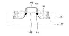
도 1은 종래 기술에 따른 PMOS 소자의 단면도를 나타낸다.1 shows a cross-sectional view of a PMOS device according to the prior art.
도 1에 도시되어 있는 바와 같이, Si로 이루어진 반도체 기판(100) 상에 SiGe 에피층(미도시)을 형성한다. 상기 SiGe 에피층의 형성은 예컨대 분자선 에피텍시(MBE) 또는 다양한 유형의 화학 기상 증착(CVD) 방법을 이용하여 수행된다.As shown in FIG. 1, a SiGe epi layer (not shown) is formed on a
이어서, NMOS 소자(미도시)와 PMOS 소자를 분리하기 위하여 반도체 기판(100)에 STI(Shallow Trench Isolation) 소자 분리막(101)을 형성하고, 상기 반도체 기판(100)에 절연층(미도시) 및 폴리실리콘층을 순차적으로 적층한 후 선택적으로 식각하여 게이트 절연막(102) 및 게이트 전극(103)을 각각 형성한다.Subsequently, a shallow trench isolation (STI)
그리고, 소스/드레인 영역에 P형 불순물 이온을 저농도로 주입함으로써 LDD(Lightly Doped Drain) 영역(104)을 형성한다. LDD 영역(104)을 형성하는 이유는, 반도체 소자의 고집적화에 따라 게이트 전극의 CD(Critical Dimension)가 작아져서 소오스/드레인 간의 채널 길이가 짧아짐에 따라 문턱 전압보다 낮은 전압의 신호에도 트랜지스터가 오동작하는 것을 방지하기 위함이다.Lightly doped drain (LDD)
이어서, 상기 게이트 절연막(102) 및 게이트 전극(103)의 측벽에 스페이서(105)를 형성하고, 상기 게이트 전극(103) 및 상기 스페이서(105)를 마스크로 하여 상기 SiGe 에피층에 상기 P형 불순물 이온을 고농도로 주입함으로써 압축적으로 변형된 에피텍셜 SiGe 소오스/드레인 영역(106)을 형성한다. 이 때, 상기 에피텍셜 SiGe 소오스/드레인 영역(106)은 약 500 내지 600 ℃의 온도에서 성장한 후 냉각됨으로써 게이트 에지 근방의 SiGe이 더욱 더 압축 변형되도록 한다. 이러한 부가적 압축 변형은 PMOS의 정공 캐리어 이동도를 더욱 향상시킨다.Subsequently, a
그러나, 이상에서 살펴본 SiGe을 이용한 신장된 에피텍셜 소오스/드레인 영역(106)의 형성은 PMOS 소자의 정공 캐리어 이동도를 향상시키기는 하지만, 제조 비용의 상승을 피할 수 없고, 공정 자체도 까다로울 뿐만 아니라, SiGe를 사용함에 따른 수율 저하 등의 결함이 수반되는 문제점이 있다.However, the formation of the extended epitaxial source /
본 발명은 상기와 같은 문제점을 해결하기 위한 것으로, SiGe 에피층을 사용하지 않으면서도 실리콘 채널에 스트레스를 유도함으로써 PMOS 소자의 정공 이동도(mobility)를 향상시킨 반도체 소자 및 그 제조 방법을 제공하는데 그 목적이 있다.SUMMARY OF THE INVENTION The present invention has been made to solve the above problems, and provides a semiconductor device and a method of manufacturing the same, which improve the hole mobility of a PMOS device by inducing stress in a silicon channel without using a SiGe epilayer. There is a purpose.
상기와 같은 목적을 달성하기 위한 본 발명에 따른 반도체 소자는, 제 1 도전형 반도체 기판; 상기 반도체 기판에 제 2 도전형 불순물이 이온 주입된 소오스/드레인 영역; 상기 소오스/드레인 영역 사이의 채널 상에 형성되는 게이트 절연막; 상기 게이트 절연막 상에 형성되는 게이트 전극; 및 상기 게이트 절연막 및 게이트 전극의 측벽에 형성되며, 산화막 및 질화막으로 이루어진 ON 구조의 스페이서를 포함하되, 상기 질화막은 불순물이 주입됨으로써 원자 사이의 결합이 파괴되는 것을 특징으로 한다.A semiconductor device according to the present invention for achieving the above object, the first conductivity type semiconductor substrate; A source / drain region in which a second conductivity type impurity is ion implanted into the semiconductor substrate; A gate insulating film formed on a channel between the source / drain regions; A gate electrode formed on the gate insulating film; And a spacer having an ON structure formed on the sidewalls of the gate insulating film and the gate electrode, wherein the nitride film has an ON structure formed of an oxide film and a nitride film.
상기의 목적을 달성하기 위한 또 다른 측면으로서의 본 발명의 반도체 소자의 제조방법은, 제 1 도전형 반도체 기판 상에 절연층 및 폴리실리콘층을 순차적으로 적층하는 단계; 상기 절연층 및 폴리실리콘층을 선택적으로 식각함으로써 게이트 절연막 및 게이트 전극을 형성하는 단계; 상기 게이트 전극을 마스크로 이용하여 상기 반도체 기판에 저농도의 제 2 도전형 불순물 이온을 주입함으로써 LDD(Lightly Doped Drain)용 저농도 불순물 영역을 형성하는 단계; 상기 게이트 전극을 포함하는 반도체 기판의 전면에 산화막을 형성하는 단계; 상기 산화막 상에 질화막을 형성하는 단계; 상기 질화막에 불순물을 주입하는 단계; 및 상기 질화막 및 산화막을 에치백함으로써 상기 게이트 절연막 및 게이트 전극의 측벽에 ON 구조의 스페이서을 형성하는 단계를 포함한다.As another aspect of the present invention, there is provided a method of manufacturing a semiconductor device, the method comprising: sequentially stacking an insulating layer and a polysilicon layer on a first conductivity type semiconductor substrate; Selectively etching the insulating layer and the polysilicon layer to form a gate insulating film and a gate electrode; Forming a low concentration impurity region for lightly doped drain (LDD) by implanting low concentration of second conductivity type impurity ions into the semiconductor substrate using the gate electrode as a mask; Forming an oxide film on an entire surface of the semiconductor substrate including the gate electrode; Forming a nitride film on the oxide film; Injecting impurities into the nitride film; And forming spacers having an ON structure on sidewalls of the gate insulating film and the gate electrode by etching back the nitride film and the oxide film.
바람직하게는, 상기 불순물은 게르마늄(Ge) 또는 아르곤(Ar)이며, 상기 질화막은 게르마늄(Ge) 또는 아르곤(Ar)이 주입됨으로써 최소한 부분적으로 원자 사이의 결합이 파괴된다.Preferably, the impurity is germanium (Ge) or argon (Ar), and the nitride film is injected with germanium (Ge) or argon (Ar) at least partially to break the bond between atoms.
이하, 첨부된 도면을 참고하여 본 발명에 의한 반도체 소자의 제조방법을 보다 상세히 설명하면 다음과 같다.Hereinafter, a method of manufacturing a semiconductor device according to the present invention will be described in detail with reference to the accompanying drawings.
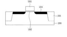
도 2a 내지 도 2e는 본 발명의 실시예에 따른 반도체 소자의 제조방법을 나타낸 공정 단면도이다.2A through 2E are cross-sectional views illustrating a method of manufacturing a semiconductor device in accordance with an embodiment of the present invention.
먼저, 도 2a에 도시한 바와 같이, 실리콘(Si)으로 이루어진 N형 반도체 기판(200) 상에 NMOS 소자(미도시)와의 분리를 위하여 STI(Shallow Trench Isolation) 소자 분리막(201)을 형성하고, 상기 반도체 기판(200)에 절연층(미도시) 및 폴리실리콘층을 순차적으로 적층한 후 선택적으로 식각하여 게이트 절연막(202) 및 게이트 전극(203)을 각각 형성한다.First, as shown in FIG. 2A, a shallow trench isolation (STI)
그리고, 상기 게이트 전극(203)을 마스크로 이용하여 반도체 기판(200) 전면에 P형 불순물 이온을 저농도로 주입함으로써 LDD(Lightly Doped Drain)용 저농도 불순물 영역(204)을 형성한다. LDD용 저농도 불순물 영역(204)을 형성하는 이유는, 반도체 소자의 고집적화에 따라 게이트 전극의 CD(Critical Dimension)가 작아져서 소오스/드레인 간의 채널 길이가 짧아짐에 따라 문턱 전압보다 낮은 전압의 신호에도 트랜지스터가 오동작하는 것을 방지하기 위함이다.A low
이어서, 도 2b에 도시되어 있는 바와 같이, 상기 게이트 전극(203)을 포함하는 반도체 기판(200)의 전면에 산화막(205)을 150 내지 250 Å 바람직하게는 약 200 Å 두께를 갖도록 형성한다. 이 때, 상기 산화막(205)의 두께가 150 Å 미만인 경우에는 이 후에 형성될 질화막에 대한 이온 주입시 실리콘 채널에 까지 영향을 미칠 수 있으며, 그 두께가 250 Å를 초과하는 경우에는 이온 주입에 따른 상기 질화막의 스트레스가 실리콘 채널에 잘 전달되지 않는 것에 주의하여야 한다. 한편, 상기 산화막은 TEOS(Tetraethoxysilane)인 것이 바람직하다.Subsequently, as illustrated in FIG. 2B, an
이어서, 도 2c에 도시되어 있는 바와 같이, 상기 산화막(205) 상에 질화막(206)을 650 내지 750 Å, 바람직하게는 약 700 Å의 두께를 갖도록 형성한다. 이 때, 상기 질화막(206)의 두께가 650 Å 미만인 경우에는 후속의 불순물 주입 공정시 실리콘 채널까지 영향을 미칠 수 있으며, 그 두께가 750 Å를 초과하는 경우에는 실리콘 채널에 가해지는 압축 스트레스가 미미해진다.Next, as illustrated in FIG. 2C, a
이어서, 도 2d에 도시되어 있는 바와 같이, 상기 질화막(206)에 불순물, 바람직하게는 게르마늄(Ge)을 주입함으로써, 상기 질화막(206)을 Ge이 주입된 질화막(206a)으로 변형시킨다. 이 때, 상기 질화막(206)은 Ge의 주입으로 인해 최소한 부분적으로 그 원자 결합이 파괴됨으로 인해 스트레스가 발생하고, 결과적으로 실리콘 채널에 압축 스트레스를 형성시킨다. 이와 같은 실리콘 채널의 압축 스트레스는 PMOS의 정공 캐리어 이동도를 크게 향상시킨다.Next, as illustrated in FIG. 2D, an impurity, preferably germanium (Ge), is injected into the
상기 Ge의 주입은 약 5 × E14 ion/cm2의 양을 약 40 내지 100 KeV의 에너지, 바람직하게는 80 KeV의 에너지를 이용하여 주입한다. 이 때, 이온 주입 에너지 가 40 KeV 미만일 경우에는 요구되는 스트레스 변화가 발생하지 않으며, 100 KeV를 초과하는 경우에는 기판(200)에 악영향을 줄 우려가 있음에 주의하여야 한다.The Ge is implanted with an amount of about 5 x E14 ions / cm2 using an energy of about 40 to 100 KeV, preferably of 80 KeV. At this time, if the ion implantation energy is less than 40 KeV, the required stress change does not occur, and if it exceeds 100 KeV, it should be noted that there is a risk that adversely affect the
한편, 주입되는 불순물은 상기 질화막(206)의 원자 결합을 파괴시킬 수 있는 것이라면 어느 것이라도 무방하나, 3가 또는 5가의 이온들은 기판에 대하여 도펀트(dopant)로서 작용을 할 수 있으므로, 4가의 게르마늄(Ge) 또는 불활성 가스인 아르곤(Ar)을 사용하는 것이 바람직하다.The implanted impurities may be any one that can break the atomic bond of the
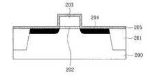
이어서, 도 2e에 도시되어 있는 바와 같이, 상기 Ge이 주입된 질화막(206a) 및 산화막(205)을 각각 선택적으로 식가함으로써 상기 게이트 절연막(202) 및 게이트 전극(203)의 측벽에 ON 구조의 스페이서(205a, 206b)를 형성한다. 그리고, 상기 게이트 전극(203) 및 상기 스페이서(205a, 206b)를 마스크로 하여 상기 반도체 기판(200)의 전면에 P형 불순물 이온을 고농도로 주입함으로써 소오스/드레인 영역(207)을 형성한다.Subsequently, as shown in FIG. 2E, the Ge-implanted
이상에서, 본 발명의 바람직한 실시예를 첨부한 도면을 참조로 하여 상세히 살펴보았으나, 본 발명의 기술적 범주를 벗어나지 않는 당업자에게 자명한 변형 내지 변화가 다양하게 존재할 것이기 때문에, 그러한 변형 내지 변화가 본 발명의 청구항 또는 그 균등물의 범위에 속한다면 본 발명의 기술적 범위에 해당하는 것으로 해석되어야 한다.In the above, preferred embodiments of the present invention have been described in detail with reference to the accompanying drawings, but such variations or modifications may be present because various modifications or changes apparent to those skilled in the art will exist without departing from the technical scope of the present invention. If it belongs to the scope of the claims or equivalents thereof, it should be construed as corresponding to the technical scope of the present invention.
이상에서 설명한 바와 같은 본 발명에 따른 반도체 소자 및 그 제조방법에 있어서는 다음과 같은 효과가 있다.As described above, the semiconductor device and the method of manufacturing the same according to the present invention have the following effects.
첫째, ON 구조 스페이서를 형성하는 통상의 공정에 단순히 Ge 주입 공정만을 추가함으로써 PMOS 소자의 정공 캐리어 이동도를 향상시킬 수 있기 때문에 SiGe을 이용하는 기술에 비해 공정 구현이 용이하다.First, since the hole carrier mobility of the PMOS device can be improved by simply adding a Ge injection process to the conventional process of forming the ON structure spacer, the process is easier to implement than the technology using SiGe.
둘째, SiGe을 이용하는 기술에 비해 저렴한 비용으로 PMOS 소자의 정공 캐리어 이동도를 향상시킬 수 있다.Second, the hole carrier mobility of the PMOS device can be improved at a lower cost than the technology using SiGe.
셋째, SiGe을 이용하지 않으면서도 PMOS 소자의 정공 캐리어 이동도를 향상시킬 수 있기 때문에, SiGe의 이용에 따른 수율 저하 문제로부터 자유롭다.Third, since the hole carrier mobility of the PMOS device can be improved without using SiGe, it is free from the yield reduction problem caused by the use of SiGe.
Claims (14)
Translated fromKoreanPriority Applications (2)
| Application Number | Priority Date | Filing Date | Title |
|---|---|---|---|
| KR1020050133823AKR100760912B1 (en) | 2005-12-29 | 2005-12-29 | Semiconductor device and manufacturing method thereof |
| US11/615,078US20070152282A1 (en) | 2005-12-29 | 2006-12-22 | Semiconductor Device and Fabrication Method Thereof |
Applications Claiming Priority (1)
| Application Number | Priority Date | Filing Date | Title |
|---|---|---|---|
| KR1020050133823AKR100760912B1 (en) | 2005-12-29 | 2005-12-29 | Semiconductor device and manufacturing method thereof |
Publications (2)
| Publication Number | Publication Date |
|---|---|
| KR20070070863A KR20070070863A (en) | 2007-07-04 |
| KR100760912B1true KR100760912B1 (en) | 2007-09-21 |
Family
ID=38223486
Family Applications (1)
| Application Number | Title | Priority Date | Filing Date |
|---|---|---|---|
| KR1020050133823AExpired - Fee RelatedKR100760912B1 (en) | 2005-12-29 | 2005-12-29 | Semiconductor device and manufacturing method thereof |
Country Status (2)
| Country | Link |
|---|---|
| US (1) | US20070152282A1 (en) |
| KR (1) | KR100760912B1 (en) |
Families Citing this family (1)
| Publication number | Priority date | Publication date | Assignee | Title |
|---|---|---|---|---|
| US20070200179A1 (en)* | 2006-02-24 | 2007-08-30 | Taiwan Semiconductor Manufacturing Co., Ltd. | Strain enhanced CMOS architecture with amorphous carbon film and fabrication method of forming the same |
Citations (6)
| Publication number | Priority date | Publication date | Assignee | Title |
|---|---|---|---|---|
| KR19980024988A (en)* | 1996-09-27 | 1998-07-06 | 로더리히 네테부쉬, 롤프 옴케 | Integrated CMOS circuit apparatus and its manufacturing method |
| KR19990010119A (en)* | 1997-07-15 | 1999-02-05 | 포만 제프리 엘 | Device for improving carrier mobility and semiconductor island forming method |
| KR20020055419A (en)* | 2000-12-28 | 2002-07-08 | 니시무로 타이죠 | A semiconductor device and manufacturing method thereof |
| KR20050041881A (en)* | 2003-10-31 | 2005-05-04 | 인터내셔널 비지네스 머신즈 코포레이션 | High mobility heterojunction complementary field effect transistors and methods thereof |
| KR20050064569A (en)* | 2003-12-24 | 2005-06-29 | 한국전자통신연구원 | Semiconductor cmos device |
| KR20050121479A (en)* | 2004-06-22 | 2005-12-27 | 삼성전자주식회사 | Fabricating method of cmos transistor and cmos transistor fabricated by the same method |
Family Cites Families (4)
| Publication number | Priority date | Publication date | Assignee | Title |
|---|---|---|---|---|
| KR100416628B1 (en)* | 2002-06-22 | 2004-01-31 | 삼성전자주식회사 | Manufacturing method for semiconductor device including gate spacer |
| US6902971B2 (en)* | 2003-07-21 | 2005-06-07 | Freescale Semiconductor, Inc. | Transistor sidewall spacer stress modulation |
| US20060014350A1 (en)* | 2004-07-18 | 2006-01-19 | Yun-Ren Wang | Method for fabricating a semiconductor transistor device having ultra-shallow source/drain extensions |
| KR100649311B1 (en)* | 2005-12-15 | 2006-11-24 | 동부일렉트로닉스 주식회사 | Modified channel layer formation method of PMOS device using gate spacer and PMOS device formed by this method |
- 2005
- 2005-12-29KRKR1020050133823Apatent/KR100760912B1/ennot_activeExpired - Fee Related
- 2006
- 2006-12-22USUS11/615,078patent/US20070152282A1/ennot_activeAbandoned
Patent Citations (6)
| Publication number | Priority date | Publication date | Assignee | Title |
|---|---|---|---|---|
| KR19980024988A (en)* | 1996-09-27 | 1998-07-06 | 로더리히 네테부쉬, 롤프 옴케 | Integrated CMOS circuit apparatus and its manufacturing method |
| KR19990010119A (en)* | 1997-07-15 | 1999-02-05 | 포만 제프리 엘 | Device for improving carrier mobility and semiconductor island forming method |
| KR20020055419A (en)* | 2000-12-28 | 2002-07-08 | 니시무로 타이죠 | A semiconductor device and manufacturing method thereof |
| KR20050041881A (en)* | 2003-10-31 | 2005-05-04 | 인터내셔널 비지네스 머신즈 코포레이션 | High mobility heterojunction complementary field effect transistors and methods thereof |
| KR20050064569A (en)* | 2003-12-24 | 2005-06-29 | 한국전자통신연구원 | Semiconductor cmos device |
| KR20050121479A (en)* | 2004-06-22 | 2005-12-27 | 삼성전자주식회사 | Fabricating method of cmos transistor and cmos transistor fabricated by the same method |
Also Published As
| Publication number | Publication date |
|---|---|
| US20070152282A1 (en) | 2007-07-05 |
| KR20070070863A (en) | 2007-07-04 |
Similar Documents
| Publication | Publication Date | Title |
|---|---|---|
| US7208362B2 (en) | Transistor device containing carbon doped silicon in a recess next to MDD to create strain in channel | |
| KR100642747B1 (en) | Method for manufacturing CMOS transistor and CMOS transistor manufactured by | |
| US7553717B2 (en) | Recess etch for epitaxial SiGe | |
| US7892931B2 (en) | Use of a single mask during the formation of a transistor's drain extension and recessed strained epi regions | |
| US7315063B2 (en) | CMOS transistor and method of manufacturing the same | |
| US7803718B2 (en) | BiCMOS performance enhancement by mechanical uniaxial strain and methods of manufacture | |
| US8114727B2 (en) | Disposable spacer integration with stress memorization technique and silicon-germanium | |
| US20080242032A1 (en) | Carbon-Doped Epitaxial SiGe | |
| US7615435B2 (en) | Semiconductor device and method of manufacture | |
| US20070267703A1 (en) | Strained channel transistor and method of fabrication thereof | |
| US20060024876A1 (en) | Methods, systems and structures for forming improved transistors | |
| US20050093021A1 (en) | High mobility heterojunction complementary field effect transistors and methods thereof | |
| US20080169490A1 (en) | Semiconductor device and manufacturing method thereof | |
| US20080017931A1 (en) | Metal-oxide-semiconductor transistor device, manufacturing method thereof, and method of improving drain current thereof | |
| KR20020066191A (en) | MOS FIELD-EFFECT TRANSISTOR COMPRISING LAYERED STRUCTURE INCLUDING Si LAYER AND SiGe LAYER OR SiGeC LAYER AS CHANNEL REGIONS | |
| JP2013545289A (en) | Method and structure for pFET junction profile with SiGe channel | |
| KR20110038594A (en) | Semiconductor device with silicon (SOL) on stress liner | |
| US20080116487A1 (en) | Methods of fabricating transistors having high carrier mobility and transistors fabricated thereby | |
| US20110306170A1 (en) | Novel Method to Improve Performance by Enhancing Poly Gate Doping Concentration in an Embedded SiGe PMOS Process | |
| KR100649311B1 (en) | Modified channel layer formation method of PMOS device using gate spacer and PMOS device formed by this method | |
| US9412869B2 (en) | MOSFET with source side only stress | |
| KR100760912B1 (en) | Semiconductor device and manufacturing method thereof | |
| KR100788353B1 (en) | Semiconductor device and manufacturing method thereof | |
| WO2011052108A1 (en) | Semiconductor device and method for manufacturing same | |
| JP2005209980A (en) | Semiconductor device and method for manufacturing the same |
Legal Events
| Date | Code | Title | Description |
|---|---|---|---|
| A201 | Request for examination | ||
| PA0109 | Patent application | St.27 status event code:A-0-1-A10-A12-nap-PA0109 | |
| PA0201 | Request for examination | St.27 status event code:A-1-2-D10-D11-exm-PA0201 | |
| PN2301 | Change of applicant | St.27 status event code:A-3-3-R10-R13-asn-PN2301 St.27 status event code:A-3-3-R10-R11-asn-PN2301 | |
| PN2301 | Change of applicant | St.27 status event code:A-3-3-R10-R13-asn-PN2301 St.27 status event code:A-3-3-R10-R11-asn-PN2301 | |
| E902 | Notification of reason for refusal | ||
| PE0902 | Notice of grounds for rejection | St.27 status event code:A-1-2-D10-D21-exm-PE0902 | |
| E13-X000 | Pre-grant limitation requested | St.27 status event code:A-2-3-E10-E13-lim-X000 | |
| P11-X000 | Amendment of application requested | St.27 status event code:A-2-2-P10-P11-nap-X000 | |
| P13-X000 | Application amended | St.27 status event code:A-2-2-P10-P13-nap-X000 | |
| PG1501 | Laying open of application | St.27 status event code:A-1-1-Q10-Q12-nap-PG1501 | |
| E701 | Decision to grant or registration of patent right | ||
| PE0701 | Decision of registration | St.27 status event code:A-1-2-D10-D22-exm-PE0701 | |
| GRNT | Written decision to grant | ||
| PR0701 | Registration of establishment | St.27 status event code:A-2-4-F10-F11-exm-PR0701 | |
| PR1002 | Payment of registration fee | St.27 status event code:A-2-2-U10-U11-oth-PR1002 Fee payment year number:1 | |
| PG1601 | Publication of registration | St.27 status event code:A-4-4-Q10-Q13-nap-PG1601 | |
| G170 | Re-publication after modification of scope of protection [patent] | ||
| PG1701 | Publication of correction | St.27 status event code:A-5-5-P10-P19-oth-PG1701 Patent document republication publication date:20080418 Republication note text:Request for Correction Notice (Document Request) Gazette number:1007609120000 Gazette reference publication date:20070921 | |
| PR1001 | Payment of annual fee | St.27 status event code:A-4-4-U10-U11-oth-PR1001 Fee payment year number:4 | |
| FPAY | Annual fee payment | Payment date:20110809 Year of fee payment:5 | |
| PR1001 | Payment of annual fee | St.27 status event code:A-4-4-U10-U11-oth-PR1001 Fee payment year number:5 | |
| FPAY | Annual fee payment | Payment date:20120827 Year of fee payment:6 | |
| PR1001 | Payment of annual fee | St.27 status event code:A-4-4-U10-U11-oth-PR1001 Fee payment year number:6 | |
| LAPS | Lapse due to unpaid annual fee | ||
| PC1903 | Unpaid annual fee | St.27 status event code:A-4-4-U10-U13-oth-PC1903 Not in force date:20130918 Payment event data comment text:Termination Category : DEFAULT_OF_REGISTRATION_FEE | |
| PC1903 | Unpaid annual fee | St.27 status event code:N-4-6-H10-H13-oth-PC1903 Ip right cessation event data comment text:Termination Category : DEFAULT_OF_REGISTRATION_FEE Not in force date:20130918 | |
| P22-X000 | Classification modified | St.27 status event code:A-4-4-P10-P22-nap-X000 |