KR100759679B1 - Supporting plate, apparatus and method for stripping supporting plate - Google Patents
Supporting plate, apparatus and method for stripping supporting plateDownload PDFInfo
- Publication number
- KR100759679B1 KR100759679B1KR1020060082653AKR20060082653AKR100759679B1KR 100759679 B1KR100759679 B1KR 100759679B1KR 1020060082653 AKR1020060082653 AKR 1020060082653AKR 20060082653 AKR20060082653 AKR 20060082653AKR 100759679 B1KR100759679 B1KR 100759679B1
- Authority
- KR
- South Korea
- Prior art keywords
- hole
- support plate
- solvent
- plate
- substrate
- Prior art date
- Legal status (The legal status is an assumption and is not a legal conclusion. Google has not performed a legal analysis and makes no representation as to the accuracy of the status listed.)
- Expired - Fee Related
Links
Images


Classifications
- H—ELECTRICITY
- H01—ELECTRIC ELEMENTS
- H01L—SEMICONDUCTOR DEVICES NOT COVERED BY CLASS H10
- H01L21/00—Processes or apparatus adapted for the manufacture or treatment of semiconductor or solid state devices or of parts thereof
- H01L21/67—Apparatus specially adapted for handling semiconductor or electric solid state devices during manufacture or treatment thereof; Apparatus specially adapted for handling wafers during manufacture or treatment of semiconductor or electric solid state devices or components ; Apparatus not specifically provided for elsewhere
- H01L21/683—Apparatus specially adapted for handling semiconductor or electric solid state devices during manufacture or treatment thereof; Apparatus specially adapted for handling wafers during manufacture or treatment of semiconductor or electric solid state devices or components ; Apparatus not specifically provided for elsewhere for supporting or gripping
- B—PERFORMING OPERATIONS; TRANSPORTING
- B29—WORKING OF PLASTICS; WORKING OF SUBSTANCES IN A PLASTIC STATE IN GENERAL
- B29C—SHAPING OR JOINING OF PLASTICS; SHAPING OF MATERIAL IN A PLASTIC STATE, NOT OTHERWISE PROVIDED FOR; AFTER-TREATMENT OF THE SHAPED PRODUCTS, e.g. REPAIRING
- B29C63/00—Lining or sheathing, i.e. applying preformed layers or sheathings of plastics; Apparatus therefor
- B29C63/0004—Component parts, details or accessories; Auxiliary operations
- B29C63/0013—Removing old coatings
- H—ELECTRICITY
- H01—ELECTRIC ELEMENTS
- H01L—SEMICONDUCTOR DEVICES NOT COVERED BY CLASS H10
- H01L21/00—Processes or apparatus adapted for the manufacture or treatment of semiconductor or solid state devices or of parts thereof
- H01L21/02—Manufacture or treatment of semiconductor devices or of parts thereof
- H01L21/04—Manufacture or treatment of semiconductor devices or of parts thereof the devices having potential barriers, e.g. a PN junction, depletion layer or carrier concentration layer
- H01L21/18—Manufacture or treatment of semiconductor devices or of parts thereof the devices having potential barriers, e.g. a PN junction, depletion layer or carrier concentration layer the devices having semiconductor bodies comprising elements of Group IV of the Periodic Table or AIIIBV compounds with or without impurities, e.g. doping materials
- H01L21/30—Treatment of semiconductor bodies using processes or apparatus not provided for in groups H01L21/20 - H01L21/26
- H01L21/302—Treatment of semiconductor bodies using processes or apparatus not provided for in groups H01L21/20 - H01L21/26 to change their surface-physical characteristics or shape, e.g. etching, polishing, cutting
- H01L21/304—Mechanical treatment, e.g. grinding, polishing, cutting
- H—ELECTRICITY
- H01—ELECTRIC ELEMENTS
- H01L—SEMICONDUCTOR DEVICES NOT COVERED BY CLASS H10
- H01L21/00—Processes or apparatus adapted for the manufacture or treatment of semiconductor or solid state devices or of parts thereof
- H01L21/67—Apparatus specially adapted for handling semiconductor or electric solid state devices during manufacture or treatment thereof; Apparatus specially adapted for handling wafers during manufacture or treatment of semiconductor or electric solid state devices or components ; Apparatus not specifically provided for elsewhere
- H01L21/683—Apparatus specially adapted for handling semiconductor or electric solid state devices during manufacture or treatment thereof; Apparatus specially adapted for handling wafers during manufacture or treatment of semiconductor or electric solid state devices or components ; Apparatus not specifically provided for elsewhere for supporting or gripping
- H01L21/687—Apparatus specially adapted for handling semiconductor or electric solid state devices during manufacture or treatment thereof; Apparatus specially adapted for handling wafers during manufacture or treatment of semiconductor or electric solid state devices or components ; Apparatus not specifically provided for elsewhere for supporting or gripping using mechanical means, e.g. chucks, clamps or pinches
- B—PERFORMING OPERATIONS; TRANSPORTING
- B29—WORKING OF PLASTICS; WORKING OF SUBSTANCES IN A PLASTIC STATE IN GENERAL
- B29L—INDEXING SCHEME ASSOCIATED WITH SUBCLASS B29C, RELATING TO PARTICULAR ARTICLES
- B29L2031/00—Other particular articles
- B29L2031/34—Electrical apparatus, e.g. sparking plugs or parts thereof
- B29L2031/3425—Printed circuits
- Y—GENERAL TAGGING OF NEW TECHNOLOGICAL DEVELOPMENTS; GENERAL TAGGING OF CROSS-SECTIONAL TECHNOLOGIES SPANNING OVER SEVERAL SECTIONS OF THE IPC; TECHNICAL SUBJECTS COVERED BY FORMER USPC CROSS-REFERENCE ART COLLECTIONS [XRACs] AND DIGESTS
- Y10—TECHNICAL SUBJECTS COVERED BY FORMER USPC
- Y10T—TECHNICAL SUBJECTS COVERED BY FORMER US CLASSIFICATION
- Y10T156/00—Adhesive bonding and miscellaneous chemical manufacture
- Y10T156/11—Methods of delaminating, per se; i.e., separating at bonding face
- Y10T156/1111—Using solvent during delaminating [e.g., water dissolving adhesive at bonding face during delamination, etc.]
- Y—GENERAL TAGGING OF NEW TECHNOLOGICAL DEVELOPMENTS; GENERAL TAGGING OF CROSS-SECTIONAL TECHNOLOGIES SPANNING OVER SEVERAL SECTIONS OF THE IPC; TECHNICAL SUBJECTS COVERED BY FORMER USPC CROSS-REFERENCE ART COLLECTIONS [XRACs] AND DIGESTS
- Y10—TECHNICAL SUBJECTS COVERED BY FORMER USPC
- Y10T—TECHNICAL SUBJECTS COVERED BY FORMER US CLASSIFICATION
- Y10T156/00—Adhesive bonding and miscellaneous chemical manufacture
- Y10T156/11—Methods of delaminating, per se; i.e., separating at bonding face
- Y10T156/1126—Using direct fluid current against work during delaminating
- Y10T156/1132—Using vacuum directly against work during delaminating
- Y—GENERAL TAGGING OF NEW TECHNOLOGICAL DEVELOPMENTS; GENERAL TAGGING OF CROSS-SECTIONAL TECHNOLOGIES SPANNING OVER SEVERAL SECTIONS OF THE IPC; TECHNICAL SUBJECTS COVERED BY FORMER USPC CROSS-REFERENCE ART COLLECTIONS [XRACs] AND DIGESTS
- Y10—TECHNICAL SUBJECTS COVERED BY FORMER USPC
- Y10T—TECHNICAL SUBJECTS COVERED BY FORMER US CLASSIFICATION
- Y10T156/00—Adhesive bonding and miscellaneous chemical manufacture
- Y10T156/19—Delaminating means
- Y10T156/1928—Differential fluid pressure delaminating means
Landscapes
- Engineering & Computer Science (AREA)
- Manufacturing & Machinery (AREA)
- Physics & Mathematics (AREA)
- Condensed Matter Physics & Semiconductors (AREA)
- General Physics & Mathematics (AREA)
- Computer Hardware Design (AREA)
- Microelectronics & Electronic Packaging (AREA)
- Power Engineering (AREA)
- Container, Conveyance, Adherence, Positioning, Of Wafer (AREA)
- Mechanical Treatment Of Semiconductor (AREA)
Abstract
Translated fromKoreanDescription
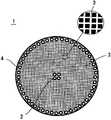
Translated fromKorean도 1은 본 발명의 서포트 플레이트의 하나의 실시형태를 나타내는 개략 구성도이다.BRIEF DESCRIPTION OF THE DRAWINGS It is a schematic block diagram which shows one Embodiment of the support plate of this invention.
도 2는 격자형상의 홈을 설명하기 위한 확대도이다.2 is an enlarged view for explaining a lattice groove.
도 3은 지그재그 형상의 홈을 설명하기 위한 확대도이다.3 is an enlarged view for explaining a zigzag groove.
도 4는 벌집형상의 홈을 설명하기 위한 확대도이다.4 is an enlarged view for explaining a honeycomb groove.
도 5는 본 발명의 서포트 플레이트의 박리장치의 하나의 실시형태를 나타내는 개략 구성도이다.It is a schematic block diagram which shows one Embodiment of the peeling apparatus of the support plate of this invention.
도 6은 도 5의 상면도이다.6 is a top view of FIG. 5.
도 7은 박리장치의 다른 실시형태를 나타내는 도면이다.It is a figure which shows another embodiment of a peeling apparatus.
도 8은 종래의 박리방법을 설명하는 도면이다(그의 1).8 is a view for explaining a conventional peeling method (1).
도 9는 종래의 박리방법을 설명하는 도면이다(그의 2).9 is a view for explaining a conventional peeling method (2).
도 10은 종래의 문제점을 설명하는 도면이다.10 is a diagram illustrating a conventional problem.
[부호의 설명][Description of the code]
1…서포트 플레이트, 2…제1의 관통구멍(貫通孔), 3…홈(溝), 4…제2의 관통구멍, 5…접착제층, 6…프레임, 7…다이싱 테이프, 10…플레이트, 12…용제 공급구 멍, 13…구멍, 14…용제 배출구멍, 15…오목부, 20…박리장치, W…반도체 웨이퍼One… Support plate, 2... First through hole, 3... Groove, 4... Second through hole, 5... Adhesive layer, 6.. Frame, 7... Dicing tape, 10... Plate, 12... Solvent Supply Holes, 13... Hole, 14... Solvent outlet hole, 15... 20 recessed portion; Peeling apparatus, W... Semiconductor wafer
본 발명은, 반도체 웨이퍼 등의 기판을 박판화(薄板化)할 때에 사용되는 서포트 플레이트, 더 나아가서는, 반도체 웨이퍼로부터 상기 서포트 플레이트를 박리하는 박리장치 및 박리방법에 관한 것이다.The present invention relates to a support plate used for thinning a substrate such as a semiconductor wafer, and furthermore, to a peeling apparatus and a peeling method for peeling the support plate from a semiconductor wafer.
IC 카드나 휴대전화의 박형화(薄型化), 소형화, 경량화가 요구되고 있어, 이 요구를 만족시키기 위해서는 삽입되는 반도체칩에 대해서도 얇은 두께의 반도체칩으로 해야한다. 이 때문에 반도체진공구멍의 토대가 되는 웨이퍼의 두께는 현재 상태에서는 125 ㎛~150 ㎛이지만, 차세대 칩용으로는 25 ㎛~50 ㎛의 두께가 요구된다고 말하여지고 있다.The thinning, miniaturization, and lightening of IC cards and mobile phones are required. In order to satisfy this demand, the semiconductor chips to be inserted must also be thin semiconductor chips. For this reason, it is said that the thickness of the wafer, which is the basis of the semiconductor vacuum hole, is 125 µm to 150 µm in the present state, but a thickness of 25 µm to 50 µm is required for the next generation chip.
종래에서는, 반도체 웨이퍼의 박판화는, 예를 들면 도 8에 나타내는 공정을 거쳐 행하여지고 있다.Conventionally, the thinning of a semiconductor wafer is performed through the process shown in FIG. 8, for example.
즉, 먼저, 반도체 웨이퍼의 회로(소자(素子)) 형성면(A면)에 보호 테이프를 첩부(貼付)하고, 이것을 반전(反轉)하여 반도체 웨이퍼의 이면(裏面)(B면)을 그라인더로 연삭하여 박판화한다. 이어서, 이 박판화된 반도체 웨이퍼의 이면을, 다이싱 프레임에 유지되어 있는 다이싱 테이프 상에 고정하고, 이 상태로 반도체 웨이퍼의 회로(소자) 형성면(A면)을 덮고 있는 보호 테이프를 박리한다. 그리고 그 다음, 다이싱장치에 의해 칩마다 분리하도록 하고 있다.That is, first, a protective tape is affixed on the circuit (element) formation surface (A surface) of a semiconductor wafer, and this is reversed, and the back surface (B surface) of a semiconductor wafer is grindered. Grinding and thinning Next, the back surface of the thinned semiconductor wafer is fixed on the dicing tape held in the dicing frame, and the protective tape covering the circuit (element) forming surface (A surface) of the semiconductor wafer is peeled in this state. . Then, the chips are separated for each chip by a dicing apparatus.
이러한 방법은 특허문헌 1에 개시되어 있다.Such a method is disclosed in
또한, 특허문헌 1에서는, 보호 테이프로서 내열성(耐熱性) 보호 테이프를 사용하고, 박리할 때에는 이 보호 테이프의 한쪽 끝에 강점착(强粘着) 테이프를 점착하여 박판화한 반도체 웨이퍼로부터 떼어내도록 하고 있다.In addition, in
또한, 특허문헌 2에서는, 보호 테이프 대신에 질화알루미늄-질화붕소 기공(氣孔) 소결체(燒結體)에 사다리형 실리콘 올리고머를 함침(含浸)시킨 보호기판을 사용하고, 이 보호기판과 반도체 웨이퍼를 열가소성 필름을 사용하여 접착함과 동시에, 박리하기 위해서는 80℃의 순수(純水)에 넣고, 3시간 유지한 후에 박리하는 것이 기재되어 있다.In addition, in
또한, 특허문헌 3에서는, 보호기판으로서 반도체 웨이퍼와 실질적으로 동일한 열팽창률의 알루미나, 질화알루미늄, 질화붕소, 탄화규소 등의 재료를 사용하는 것이 기재되어 있다.In addition,
또한 특허문헌 3에서는, 보호기판과 반도체 웨이퍼를 폴리이미드 등의 열가소성 수지를 사용하여 접착하고, 그라인더로 박판화한 후, 박리하는 경우에는 물, 아민 또는 물과 아민의 혼합용액 중에 침지(浸漬)하는 방법, 또는 수증기를 사용하는 방법이 제안되어 있다.Further, in
[특허문헌 1] 일본국 특허공개 제2002-270676호 공보[Patent Document 1] Japanese Patent Publication No. 2002-270676
[특허문헌 2] 일본국 특허공개 제2002-203821호 공보[Patent Document 2] Japanese Patent Publication No. 2002-203821
[특허문헌 3] 일본국 특허공개 제2001-077304호 공보[Patent Document 3] Japanese Patent Application Laid-Open No. 2001-077304
전술한 각 선행기술에 있어서는, 반도체 웨이퍼로부터 서포트 플레이트(보호 테이프)를 박리할 때에, 서포트 플레이트(보호 테이프)와 반도체 웨이퍼의 사이에 용제가 침입하기 어려워 박리에 시간이 걸려버린다.In each of the above prior arts, when peeling the support plate (protective tape) from the semiconductor wafer, it is difficult for the solvent to penetrate between the support plate (protective tape) and the semiconductor wafer, which takes time for peeling.
또한, 서포트 플레이트(보호 테이프)와 반도체 웨이퍼를 접착하고 있는 열가소성 필름이 완전히 녹지 않고 서포트 플레이트 또는 반도체 웨이퍼의 한쪽에 부착된 채 남아버리는 경우가 있다.Moreover, the thermoplastic film which adhere | attaches the support plate (protective tape) and a semiconductor wafer may remain attached to one of a support plate or a semiconductor wafer, without melt | dissolving completely.
이와 같이, 접착제의 잔사(殘渣)가 발생하는 박리시에 반도체 웨이퍼에 깨짐이나 빠짐이 발생하기 쉽다.In this way, cracks or omissions are likely to occur in the semiconductor wafer at the time of peeling where the residue of the adhesive occurs.
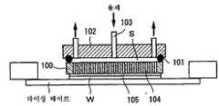
따라서, 본 출원인은 서포트 플레이트로서 두께방향으로 다수의 관통구멍이 형성된 것을 제안하고 있다. 도 9는, 이 서포트 플레이트를 박리하는 방법을 설명한 것이다.Therefore, the applicant proposes that a plurality of through holes are formed in the thickness direction as the support plate. 9 illustrates a method of peeling this support plate.
이 방법은, 먼저, 서포트 플레이트(100)의 윗면에 O링(101)을 매개로 하여 용제 공급 플레이트(102)를 쌓아 올린다. 이어서, 서포트 플레이트(100), O링(101) 및 용제 공급 플레이트(102)로 둘러싸인 공간(S)에 용제 공급관(103)으로부터 용제를 공급한다. 이에 따라, 서포트 플레이트(100)에 형성된 관통구멍(104)를 매개로 하여 접착제층(105)를 용해하도록 한 것이다.In this method, first, the
이와 같은 다수의 관통구멍을 형성한 서포트 플레이트를 사용한 방법의 경우, 단시간 사이에 확실히 접착제를 제거할 수 있지만, 새로운 문제가 발생하였다.In the case of using the support plate having such a large number of through holes, the adhesive can be reliably removed in a short time, but a new problem has arisen.
즉, 도 10에 나타내는 바와 같이, 서포트 플레이트의 둘레 가장자리부(周緣部)로부터 용제가 바깥쪽으로 새고, 다이싱 테이프에 대량의 용제가 낙하하여, 다 이싱 테이프가 단시간 사이에 열화(劣化)되어 버린다.That is, as shown in FIG. 10, a solvent leaks outward from the circumferential edge part of a support plate, a large amount of solvent falls to a dicing tape, and a dicing tape deteriorates in a short time. .
또한, 공간(S)에 공급된 신규한 용제의 일부는 그대로 회수되어 버려 박리효율이 나쁘다.In addition, part of the novel solvent supplied to the space S is recovered as it is, resulting in poor peeling efficiency.
또한, 접착제가 완전히 용해된 경우에도, 반도체 웨이퍼로부터 서포트 플레이트를 박리하기 위한 장치로서 핑거(finger) 등을 사용하면 회로 형성면을 흠집내어 버릴 우려가 있다.In addition, even when the adhesive is completely dissolved, the use of a finger or the like as a device for peeling the support plate from the semiconductor wafer may damage the circuit formation surface.
전술한 점에 비추어, 본 발명은, 예를 들면 기판을 박판화한 후에, 기판으로부터는 서포트 플레이트를 단시간에 용이하게 박리하는 것을 가능하게 하는 서포트 플레이트, 서포트 플레이트의 박리장치 및 박리방법을 제공한다.In view of the foregoing, the present invention provides a support plate, a peeling apparatus for a support plate, and a peeling method that enable, for example, to easily peel a support plate from a substrate in a short time after thinning the substrate.
본 발명의 서포트 플레이트는, 한쪽 면에 접착제를 매개로 하여 기판의 회로 형성면이 첩합(貼合)되는 서포트 플레이트로서, 서포트 플레이트의 중앙부근에 있어서 두께방향으로 형성된 제1의 관통구멍과, 서포트 플레이트의 접착제와 접하는 한쪽 면에 형성된 관통구멍에 연통(連通)하는 홈과, 서포트 플레이트의 둘레 가장자리부에 있어서 두께방향으로 형성된 홈에 연통하는 제2의 관통구멍을 갖는 구성으로 한다.The support plate of this invention is a support plate by which the circuit formation surface of a board | substrate is bonded to one surface via an adhesive agent, The 1st through-hole formed in the thickness direction near the center of a support plate, and a support It is set as the structure which has the groove which communicates with the through hole formed in the one surface which contact | connects the adhesive agent of a plate, and the 2nd through hole which communicates with the groove formed in the thickness direction in the peripheral part of a support plate.
본 발명의 서포트 플레이트에 의하면, 서포트 플레이트의 중앙부근에 있어서 두께방향으로 형성된 제1의 관통구멍과, 서포트 플레이트의 접착제와 접하는 한쪽 면에 형성된 관통구멍에 연통하는 홈과, 서포트 플레이트의 둘레 가장자리부에 있어서 두께방향으로 형성된 홈에 연통하는 제2의 관통구멍을 갖기 때문에, 예를 들 면 제1의 관통구멍은 용제가 공급되는 구멍이고, 제2의 관통구멍은 용제가 배출되는 구멍인 구성으로 하여, 실제로 기판을 박판화한 후에 기판으로부터 서포트 플레이트를 박리할 때에는, 기판과 서포트 플레이트를 첩합시키고 있는 접착제의 전면(全面)에 신속하게 고르게 용제를 공급할 수 있어, 단시간에 서포트 플레이트를 박리하는 것이 가능해진다.According to the support plate of the present invention, the first through hole formed in the thickness direction near the center of the support plate, the groove communicating with the through hole formed in one surface of the support plate in contact with the adhesive, and the peripheral portion of the support plate Since the second through hole communicates with the groove formed in the thickness direction, the first through hole is a hole through which a solvent is supplied, and the second through hole is a hole through which the solvent is discharged. Therefore, when peeling the support plate from the substrate after actually thinning the substrate, the solvent can be quickly and evenly supplied to the entire surface of the adhesive bonding the substrate and the support plate, and the support plate can be peeled off in a short time. Become.
또한, 예를 들면 제2의 관통구멍은 용제가 공급되는 구멍이고, 제1의 관통구멍은 용제가 배출되는 구멍인 구성으로 한 경우에도 이와 동일한 작용을 얻을 수 있다.For example, the same effect can be obtained when the second through hole is a hole through which a solvent is supplied, and the first through hole is a hole through which a solvent is discharged.
본 발명의 박리장치는, 기판의 회로소자 형성면에 접착제를 매개로 하여 첩합된 서포트 플레이트를 박리하는 박리장치에 있어서, 이 박리장치는 플레이트를 구비하고 있고, 이 플레이트는 그의 중앙부근에 있어서 두께방향으로 형성된 제1의 관통구멍과, 그의 둘레 가장자리부에 있어서 두께방향으로 형성된 제2의 관통구멍과, 그의 직경방향에 있어서 제1의 관통구멍과 제2의 관통구멍의 사이에 형성된 서포트 플레이트를 흡착하기 위한 구멍을 갖는 구성이다.The peeling apparatus of this invention is a peeling apparatus which peels the support plate bonded together by the adhesive agent to the circuit element formation surface of a board | substrate, This peeling apparatus is provided with the plate, and this plate is thick in the vicinity of the center part. The first through hole formed in the direction, the second through hole formed in the thickness direction in the peripheral portion thereof, and the support plate formed between the first through hole and the second through hole in the radial direction thereof. It is the structure which has a hole for adsorption.
본 발명의 박리장치에 의하면, 박리장치는 플레이트를 구비하고 있고, 이 플레이트는 그의 중앙부근에 있어서 두께방향으로 형성된 제1의 관통구멍과, 그의 둘레 가장자리부에 있어서 두께방향으로 형성된 제2의 관통구멍과, 그의 직경방향에 있어서 제1의 관통구멍과 제2의 관통구멍의 사이에 형성된 서포트 플레이트를 흡착하기 위한 구멍을 갖기 때문에, 예를 들면 제1의 관통구멍은 용제가 공급되는 구멍이고, 제2의 관통구멍은 용제가 배출되는 구멍인 구성으로 하여, 실제로 기판을 박 판화한 후에 기판으로부터 서포트 플레이트를 박리할 때에는, 기판과 서포트 플레이트를 첩합시키고 있는 접착제의 전면에 신속하게 고르게 용제를 공급할 수 있어, 단시간에 서포트 플레이트를 박리할 수 있다.According to the peeling apparatus of this invention, a peeling apparatus is provided with a plate, This plate has the 1st through hole formed in the thickness direction in the vicinity of the center part, and the 2nd penetration formed in the thickness direction in the circumferential edge part. Since the hole has a hole for adsorbing the support plate formed between the first through hole and the second through hole in the radial direction thereof, for example, the first through hole is a hole to which a solvent is supplied. The second through hole is a hole through which the solvent is discharged. When the support plate is peeled off from the substrate after actually thinning the substrate, it is possible to quickly and evenly supply the solvent to the entire surface of the adhesive bonding the substrate and the support plate. The support plate can be peeled off in a short time.
또한, 예를 들면, 제2의 관통구멍은 용제가 공급되는 구멍이고, 제1의 관통구멍은 용제가 배출되는 구멍인 구성으로 한 경우에도 이와 동일한 작용을 얻을 수 있다.For example, the same effect can be obtained when the second through hole is a hole through which a solvent is supplied, and the first through hole is a hole through which a solvent is discharged.
본 발명의 박리방법은, 기판의 회로소자 형성면에 접착제를 매개로 하여 첩합된 서포트 플레이트를 박리장치를 사용하여 박리하는 박리방법에 있어서, 플레이트의 제1의 관통구멍에 외부로부터 용제를 공급하는 공정과, 용제를 서포트 플레이트의 제1의 관통구멍을 매개로 하여 이 제1의 관통구멍에 통하는 홈에 고루 미치게 하는 공정과, 용제에 의해 기판과 접하는 면의 접착제를 용해시키는 공정과, 접착제를 용해한 용제를, 서포트 플레이트의 제2의 관통구멍을 매개로 하여, 플레이트의 제2의 관통구멍으로부터 배출시키는 공정을 갖도록 한다.The peeling method of this invention is a peeling method of peeling the support plate bonded together with the adhesive agent to the circuit element formation surface of a board | substrate using a peeling apparatus, and supplying a solvent from the outside to the 1st through-hole of a plate. The process, the step of spreading the solvent evenly through the grooves passing through the first through hole through the first through hole of the support plate, the step of dissolving the adhesive on the surface in contact with the substrate by the solvent, and the adhesive The dissolved solvent is discharged from the second through hole of the plate via the second through hole of the support plate.
전술한 본 발명의 박리방법에 의하면, 플레이트의 제1의 관통구멍에 외부로부터 용제를 공급하는 공정과, 용제를 서포트 플레이트의 제1의 관통구멍을 매개로 하여 이 제1의 관통구멍에 통하는 홈에 고루 미치게 하는 공정과, 용제에 의해 기판과 접하는 면의 접착제를 용해시키는 공정과, 접착제를 용해한 용제를 서포트 플레이트의 제2의 관통구멍을 매개로 하여, 플레이트의 제2의 관통구멍으로부터 배출시키는 공정을 갖기 때문에, 기판과 서포트 플레이트를 첩합시키고 있는 접착제의 전면에 신속하게 고르게 용제를 공급할 수 있고, 단시간에 서포트 플레이트를 박리 할 수 있다.According to the peeling method of this invention mentioned above, the process of supplying a solvent from the outside to the 1st through-hole of a plate, and the groove | channel which passes a solvent through this 1st through-hole through the 1st through-hole of a support plate. The step of dispersing the adhesive, the step of dissolving the adhesive on the surface in contact with the substrate by the solvent, and the solvent dissolving the adhesive from the second through hole of the plate through the second through hole of the support plate. Since a process is provided, a solvent can be supplied quickly and evenly to the whole surface of the adhesive bonding a board | substrate and a support plate, and a support plate can be peeled off in a short time.
또한, 본 발명의 박리방법은, 기판의 회로소자 형성면에 접착제를 매개로 하여 첩합된 서포트 플레이트를 박리장치를 사용하여 박리하는 박리방법에 있어서, 플레이트의 제2의 관통구멍에 외부로부터 용제를 공급하는 공정과, 용제를 서포트 플레이트의 제2의 관통구멍을 매개로 하여 이 제2의 관통구멍에 연통하는 홈에 고루 미치게 하는 공정과, 용제에 의해 기판과 접하는 면의 접착제를 용해시키는 공정과, 접착제를 용해한 용제를 서포트 플레이트의 제1의 관통구멍을 매개로 하여, 플레이트의 제1의 관통구멍으로부터 배출시키는 공정을 갖도록 한다.Moreover, the peeling method of this invention WHEREIN: The peeling method of peeling the support plate bonded together with the adhesive agent to the circuit element formation surface of a board | substrate using a peeling apparatus, WHEREIN: The solvent is supplied to the 2nd through hole of a plate from the outside. Supplying the solvent, spreading the solvent evenly into the groove communicating with the second through hole through the second through hole of the support plate, dissolving the adhesive on the surface of the substrate in contact with the substrate by the solvent; The solvent in which the adhesive is dissolved is discharged from the first through hole of the plate via the first through hole of the support plate.
전술한 본 발명의 박리방법에 의하면, 플레이트의 제2의 관통구멍에 외부로부터 용제를 공급하는 공정과, 용제를 서포트 플레이트의 제2의 관통구멍을 매개로 하여 이 제2의 관통구멍에 연통하는 홈에 고루 미치게 하는 공정과, 용제에 의해 기판과 접하는 면의 접착제를 용해시키는 공정과, 접착제를 용해한 용제를 서포트 플레이트의 제1의 관통구멍을 매개로 하여 플레이트의 제1의 관통구멍으로부터 배출시키는 공정을 갖기 때문에, 기판과 서포트 플레이트를 첩합시키고 있는 접착제의 전면에 신속하게 고르게 용제를 공급할 수 있고, 단시간에 서포트 플레이트를 박리할 수 있다.According to the peeling method of this invention mentioned above, the process of supplying a solvent from the outside to the 2nd through hole of a plate, and communicating a solvent with this 2nd through hole through the 2nd through hole of a support plate The step of making the groove even, the step of dissolving the adhesive on the surface contacting the substrate by the solvent, and the solvent dissolving the adhesive is discharged from the first through hole of the plate through the first through hole of the support plate. Since it has a process, a solvent can be supplied quickly and evenly to the whole surface of the adhesive bonding a board | substrate and a support plate, and a support plate can be peeled off in a short time.
이하에 본 발명의 실시형태를 첨부도면을 토대로 설명한다.EMBODIMENT OF THE INVENTION Below, embodiment of this invention is described based on an accompanying drawing.
도 1은, 본 발명의 서포트 플레이트의 하나의 실시형태를 나타내는 개략 구성도이고, 도 2는, 홈의 형성방법을 설명하기 위한 공정도이다.FIG. 1: is a schematic block diagram which shows one Embodiment of the support plate of this invention, and FIG. 2 is process drawing for demonstrating the formation method of a groove | channel.
본 실시형태의 서포트 플레이트(1)은, 도 1에 나타내는 바와 같이, 유리판, 세라믹판 또는 금속판 등으로부터 형성되어 있다.The
이 서포트 플레이트(1)의 한쪽 면에는, 도시하지 않지만, 접착제층을 매개로 하여 반도체 웨이퍼(W)의 회로 형성면이 첩합된다.Although not shown, the circuit forming surface of the semiconductor wafer W is bonded to one surface of the
그리고, 본 실시형태에 있어서는 특히, 서포트 플레이트(1)이 다음에 나타내는 바와 같이 구성되어 있다.And in this embodiment, especially the
구체적으로는, 서포트 플레이트(1)의 중앙부근(중앙부)에 외부로부터 용제가 공급되는 제1의 관통구멍(2)가 두께방향으로 관통하여 형성되어 있다. 이 관통구멍(2)는 예를 들면 복수 형성되어 있다. 또한, 도 1에 나타내는 경우에서는 4개의 관통구멍(2)를 나타냈지만 관통구멍(2)의 수는 이에 한정되지 않는다.Specifically, the first through
또한, 서포트 플레이트(1)의 반도체 웨이퍼(W)가 첩합되는 한쪽 면에는, 관통구멍(2)와 연통하는 홈(3)이 형성되어 있다. 이 홈(3)은, 한쪽 면에 있어서 바깥주위(外周)까지의 거의 전역에 걸쳐 형성되어 있다. 덧붙여서 말하자면, 예를 들면 두께 0.7 ㎜의 서포트 플레이트(1)에 대하여, 홈(3)은 한쪽 면의 표면으로부터 0.3 ㎜의 깊이로 형성되어 있다. 여기에서, 홈(3)의 깊이는, 서포트 플레이트(1)과 반도체 웨이퍼(W)를 첩합시켰을 때에 사이에 개재(介在)되는 접착제층에서 완전히 묻히지 않는 정도의 깊이가 필요해진다. 이것은, 접착제층과 홈(3)의 저면(底面)의 사이에 약간의 극간(隙間)을 만듦으로써, 후술하는 바와 같이 용제가 공급된 때에 이 극간을 타고 용제가 신속하게 흐르게 되기 때문이다.Moreover, the groove |
또한, 서포트 플레이트(1)의 둘레 가장자리부에는, 홈(3)과 연통하여 용제가 외부로 배출(회수)되는 제2의 관통구멍(4)가 두께방향으로 관통하여 형성되어 있 다. 이 관통구멍(4)는 예를 들면 서포트 플레이트(1)의 둘레 가장자리부에 복수 형성되어 있다.Further, at the peripheral edge portion of the
이상의 구성으로부터, 서포트 플레이트(1)에 있어서는, 외부로부터 용제가 공급되는 제1의 관통구멍(2)와 용제가 외부로 배출되는 제2의 관통구멍(4)가 홈(3)을 매개로 하여 연통되어 있게 된다.From the above structure, in the
홈(3)은, 도 1 중에 그의 일부의 확대도를 나타내는 바와 같이 격자(格子)형상으로 형성되어 있다. 이 홈(3)은, 전술한 바와 같이, 제1의 관통구멍(2)와 제2의 관통구멍(4)를 연통시키고 있기 때문에, 예를 들면 제1의 관통구멍(2)로 외부로부터 공급된 용제는, 이 격자형상의 홈(3)을 매개로 하여 중앙부근으로부터 둘레 가장자리부(바깥주위부)를 향해 흘러 제2의 관통구멍(4)에 이른다.The
여기에서, 격자형상의 홈(3)을 갖는 서포트 플레이트(1)을 형성하는 방법을 도 2의 공정도를 사용하여 간단하게 설명한다.Here, a method of forming the
먼저, 예를 들면 유리판을 준비하고, 홈(3)을 형성하는 한쪽 면에 드라이필름 레지스트를 도포한다(공정 1).First, a glass plate is prepared, for example, and a dry film resist is apply | coated to one surface which forms the groove | channel 3 (process 1).
이어서, 격자형상의 포토 마스크를 사용하여, 드라이필름 레지스트에 대하여 노광(露光) 및 현상(現像)처리를 행한다(공정 2 및 3 참조).Subsequently, exposure to light and development are performed on the dry film resist using a lattice-shaped photo mask (see
이에 따라, 유리판의 한쪽 면에는 격자형상의 드라이필름 레지스트(격자형상의 홈(3) 형성용 레지스트 마스크)가 형성된다.Thereby, a lattice-like dry film resist (resist mask for forming the lattice grooves 3) is formed on one surface of the glass plate.
이어서, 둘레 가장자리부를 보호한 후, 격자형상의 드라이필름 레지스트를 마스크로서 샌드 블라스트법(sand blast method)에 의해 유리판을 절삭(切削)한다 (공정 4 및 5 참조).Subsequently, after protecting the periphery, the glass plate is cut by the sand blast method using a lattice-like dry film resist (see
이에 따라, 유리기판의 한쪽 면에는 그 표면으로부터 소정의 깊이에 격자형상의 홈(3)이 형성된다.As a result, a
이어서, 유리기판의 다른 쪽 면에 드라이필름 레지스트를 도포한다(공정 6 참조).Next, a dry film resist is applied to the other side of the glass substrate (see step 6).
그리고, 제1의 관통구멍(2) 및 제2의 관통구멍(4) 형성용 포토 마스크를 사용하여, 드라이필름 레지스트에 대하여 노광 및 현상처리를 행한다(공정 7 및 공정 8 참조).Then, exposure and development are performed on the dry film resist using the photomasks for forming the first through
이에 따라, 유리판의 다른 쪽 면에는 제1의 관통구멍(2) 및 제2의 관통구멍(4)에 상당하는 드라이필름 레지스트(제1의 관통구멍(2) 및 제2의 관통구멍(4) 형성용 레지스트 마스크)가 형성된다.Accordingly, dry film resists (first through
이어서, 둘레 가장자리부를 보호한 후(공정 9 참조), 제1의 관통구멍(2) 및 제2의 관통구멍(4) 형성용 레지스트를 마스크로서 샌드 블라스트법에 의해 유리판을 절삭한다(공정 10 참조).Subsequently, after protecting the circumferential edge (refer to step 9), the glass plate is cut by the sand blasting method using the resist for forming the first through
그 다음, 유리기판 상을 세정함으로써(공정 11 참조), 유리기판의 다른 쪽 면에 있어서는 중앙부근에 두께방향으로 관통하는 제1의 관통구멍(2)가 형성되고, 둘레 가장자리 부분에 두께방향으로 관통하는 제2의 관통구멍(4)가 형성된다.Then, by cleaning the glass substrate (see Step 11), on the other side of the glass substrate, a first through
또한, 도 2에 나타내는 공정에서는, 먼저 홈(3)을 형성한 후에 제1의 관통구멍(2) 및 제2의 관통구멍(4)를 형성한 경우를 나타내었지만, 이 순서를 반대로 하는 것도 가능하다.In addition, although the process shown in FIG. 2 showed the case where the 1st through-
또한, 샌드 블라스트법 이외에도 드라이 에칭법(dry etching method)이나 웨트 에칭법(wet etching method)을 사용하여 격자형상의 홈을 형성하는 것도 가능하다. 그러나, 이들의 방법을 사용한 경우, 홈의 폭, 깊이 등에 따라 다르기도 하지만, 샌드 블라스트법에 비하여 균일한 홈의 형성이 어렵다. 이러한 점으로부터 홈(3)의 형성에는 샌드 블라스트법이 적합하다.In addition to the sand blasting method, it is also possible to form a lattice groove by using a dry etching method or a wet etching method. However, when these methods are used, the grooves may vary depending on the width, depth and the like of the grooves. From this point of view, the sand blasting method is suitable for forming the
본 실시형태의 서포트 플레이트(1)에 의하면, 중앙부근에, 외부로부터 용제가 공급되는 관통구멍(2)가 두께방향으로 형성되고, 접착제와 접촉하는 한쪽 면에, 제1의 관통구멍(2)에 연통하는 격자상의 홈(3)이 형성되며, 둘레 가장자리부에, 홈(3)에 연통함과 동시에, 용제가 외부로 배출되는 제2의 관통구멍(4)가 두께방향으로 형성되어 있기 때문에, 실제로 후술하는 박리장치 및 박리방법을 사용하여 반도체 웨이퍼(W)로부터 서포트 플레이트(1)을 박리할 때에, 웨이퍼(W)와 서포트 플레이트(1)을 첩합시키고 있는 접착제의 전면에 신속하게 고르게 용제를 공급시키는 것이 가능해진다. 이에 따라, 예를 들면 종래의 서포트 플레이트를 사용한 경우에 비하여, 단시간에 서포트 플레이트(1)을 박리하는 것이 가능해진다.According to the
즉, 종래의 서포트 플레이트의 구조는 두께방향으로 다수의 관통구멍이 형성된 구성이기 때문에 접착제는 각 관통구멍에 접하고 있는 부분부터 용해되기 시작한다. 이 때문에, 접착제의 전체에 용제가 구석구석까지 고루 미칠 때까지 시간을 요하고 있었다.That is, since the conventional support plate has a structure in which a plurality of through holes are formed in the thickness direction, the adhesive starts to dissolve from the portion in contact with each through hole. For this reason, time was required until a solvent spread | dispersed evenly to every corner of the whole adhesive agent.
그러나, 본 실시형태에 있어서의 서포트 플레이트(1)의 경우, 접착제에 접하는 면의 거의 전역에 격자형상의 홈(3)이 형성되어 있기 때문에, 제1의 관통구 멍(2)로부터 공급된 용제는 이 관통구멍(2)와 연통하는 격자형상의 홈(3)을 매개로 하여 둘레 가장자리부로 흐르고, 접착제의 전체에 용제가 신속하게 구석구석까지 고루 미친다.However, in the case of the
따라서, 예를 들면 종래의 서포트 플레이트를 사용한 경우에 비하여 단시간에 서포트 플레이트(1)을 박리하는 것이 가능해진다.Therefore, for example, it becomes possible to peel off the
또한, 종래와 같이 두께방향으로 다수의 관통구멍이 형성되어 있지 않기 때문에, 후술하는 박리장치 및 박리방법을 사용하여 실제로 반도체 웨이퍼(W)로부터 서포트 플레이트(1)을 박리할 때에는 구멍이 없는 개소를 진공흡착으로 유지하는 것이 가능해진다. 이에 따라, 반도체 웨이퍼(W)로부터 서포트 플레이트(1)을 박리하는 공정을 간소화시키는 것이 가능해진다.In addition, since a large number of through holes are not formed in the thickness direction as in the prior art, when the
또한, 종래와 같이 두께방향으로 다수의 관통구멍이 형성되어 있지 않기 때문에, 서포트 플레이트(1)로서의 강도를 향상시킬 수 있고, 종래의 서포트 플레이트에 비하여 재이용률을 더욱 높일 수 있다.In addition, since a large number of through holes are not formed in the thickness direction as in the prior art, the strength as the
또한, 이와 같이 반도체 웨이퍼(W)로부터 서포트 플레이트(1)을 박리할 때에 웨이퍼(W)에 무리한 힘이 작용하지 않기 때문에 웨이퍼(W)에 깨짐이나 빠짐이 발생하기 어렵다.In addition, since excessive force does not act on the wafer W when the
이에 따라, 이러한 서포트 플레이트(1)이 첩합된 반도체 웨이퍼(W)에 있어서는, 예를 들면 웨이퍼(W)가 박판화된 후 그라인더를 가한 면을 예를 들면 제2의 회로 형성면으로 하는 것이 가능해진다.As a result, in the semiconductor wafer W on which the
이어서, 본 실시형태의 서포트 플레이트(1)의 다른 실시형태를 설명한다.Next, another embodiment of the
전술한 실시형태의 서포트 플레이트(1)에서는 홈(3)의 형상을 격자형상으로 하였지만, 본 실시형태의 서포트 플레이트(1)에서는, 홈(3)의 형상을 지그재그 형상으로 하는 것도 가능하다(도 3(a)의 홈의 확대도 및 도 3(b)의 둘레 가장자리부의 확대도 참조).In the
즉, 본 실시형태의 서포트 플레이트(1)에서는, 홈의 형상은 도 1에 나타낸 격자형상의 홈(3)에 있어서 열마다 겹치지 않도록 소정의 간격 조금 옮긴 구성이다.That is, in the
이와 같이, 지그재그 형상의 홈(3)으로 한 경우에 있어서도, 격자형상의 홈(3)의 경우와 동일하게 웨이퍼(W)와 서포트 플레이트(1)을 첩합시키고 있는 접착제의 전면에 지그재그 형상의 홈(3)을 매개로 하여 용제를 신속하게 고르게 공급할 수 있다. 이에 따라, 종래의 서포트 플레이트를 사용한 경우에 비하여 서포트 플레이트(1)을 기판으로부터 단시간에 박리시키는 것이 가능해진다.Thus, also in the case of making the
또한, 이러한 형상의 홈(3)을 형성하는 경우도 도 2에 나타낸 공정과 동일하게 행할 수 있다.In addition, when forming the groove |
이어서, 본 실시형태의 서포트 플레이트의 추가의 다른 실시형태를 설명한다.Next, further another embodiment of the support plate of this embodiment is described.
본 실시형태의 서포트 플레이트(1)은 홈의 형상이 벌집(honeycomb)형상으로 형성되어 있다. 구체적으로는 홈(3)이 거북이 등딱지 형상(정육각형)으로 형성되어 있다(도 4(a)의 홈의 확대도 및 도 4(b)의 둘레 가장자리부의 확대도 참조).In the
이와 같이, 거북이 등딱지 형상의 홈(3)으로 한 경우는, 전술한 격자형상의 홈(3)이나 지그재그 형상의 홈(3)의 경우에 비하여 웨이퍼(W)와 서포트 플레이트(1)을 첩합시키고 있는 접착제의 전면에 거북이 등딱지 형상의 홈(3)을 매개로 하여 용제를 보다 신속하게 고르게 공급시킬 수 있고, 기판으로부터 서포트 플레이트(1)을 종래의 서포트 플레이트를 사용한 경우에 비하여 더욱 단시간에 박리시키는 것이 가능해진다.As described above, when the
그 이유로서는, 거북이 등딱지 형상의 홈(3)의 경우, 격자형상이나 지그재그 형상의 홈(3)에 비하여, 서로 인접하는 각 거북이 등딱지 형상의 홈(3)이 각각 중앙부근으로부터 둘레 가장자리부로 향하도록 형성되기 때문에, 중앙부근으로부터 공급된 용제가 둘레 가장자리부로 고루 미치기 쉬운 것이 하나의 이유로서 생각되어진다.The reason for this is that in the case of the turtle carapace-
또한, 이러한 거북이 등딱지 형상의 홈(3)을 형성하는 경우도 도 2에 나타낸 공정과 동일하게 하여 행할 수 있다.Moreover, when forming the
또한, 홈(3)의 형상으로서는, 전술한 각 형상 이외에도 용제 공급구멍(12)를 중심으로 하여 둘레 가장자리부에 형성된 용제 배출구멍(14)로 향하는 소용돌이 형상의 홈을 형성하는 것도 가능하다.As the shape of the
또한, 서포트 플레이트로서는, 다음에 나타내는 구성, 소위 젖빛유리(frosted glass)로 한 구성으로 하는 것도 가능하다.Moreover, as a support plate, it is also possible to set it as the structure shown next and what was called frosted glass.
구체적으로는, 도시하지 않아도, 반도체 웨이퍼(W)가 첩합되는 유리기판의 표면을 0.05 ㎜~0.1 ㎜ 정도 부순 구성으로 한다. 또한, 다른 구성은 전술한 각 실시형태의 서포트 플레이트(1)의 경우와 동일하기 때문에 중복 설명은 생략한다.Specifically, even if not shown, the surface of the glass substrate on which the semiconductor wafer W is bonded is made to have a structure of approximately 0.05 mm to 0.1 mm. In addition, since another structure is the same as that of the
이러한 구성의 서포트 플레이트로 한 경우는, 제1의 관통구멍(2)로부터 용제가 모세관 현상을 이용하여 전면에 침투한다. 이에 따라 전술한 각 홈(3)을 서포트 플레이트(1)의 경우와 동일한 작용을 얻을 수 있다.In the case of the support plate having such a configuration, the solvent penetrates into the entire surface from the first through
이어서, 반도체 웨이퍼(W)로부터 전술한 구성의 서포트 플레이트를 박리할 때에 사용되는, 본 발명의 박리장치 및 박리방법의 하나의 실시형태를, 도 5 및 도 6을 사용하여 설명한다.Next, one Embodiment of the peeling apparatus and peeling method of this invention used when peeling the support plate of the structure mentioned above from the semiconductor wafer W is demonstrated using FIG. 5 and FIG.
또한, 본 실시형태에 있어서는, 도 4에 나타낸 거북이 등딱지 형상의 홈(3)을 갖는 서포트 플레이트(1)을 사용한 경우를 들어 설명한다.In addition, in this embodiment, the case where the
본 실시형태의 박리장치(20)은 플레이트(10)을 구비하고 있다. 이 플레이트(10)은 승강기구에 지지되어 있고 상하방향으로 소정의 스트로크로 승강 가능하게 구성되어 있다.The peeling apparatus 20 of this embodiment is provided with the
플레이트(10)에는 중앙부에 외부로부터 용제가 공급되는 제1의 관통구멍(용제 공급구멍)(12)가 형성되어 있다. 또한, 둘레 가장자리부에는 접착제층을 용해한 용제가 외부로 배출되는 제2의 관통구멍(용제 배출구멍)(14)가 형성되어 있다. 또한, 직경방향에 있어서 제1의 관통구멍(12)와 제2의 관통구멍(14)의 사이에는 구멍(13)이 형성되어 있다. 이 구멍(13)은 진공구멍으로 되어 있고 서포트 플레이트(1)과 접하는 쪽은 오목부(15)로 되어 있다. 제1의 관통구멍(12)는, 도시하지 않지만 예를들면 튜브를 매개로 하여 용제 공급수단과 접속되어 있다.In the
이러한 구성의 플레이트(10)에 구멍(13)을 통하여 진공 흡착에 의해 서포트 플레이트(1) 및 이 서포트 플레이트(1)에 첩합된 반도체 웨이퍼(W)를 흡착시킨 경 우는, 용제 공급구멍(12)는 서포트 플레이트(1)의 제1의 관통구멍(2)에 접속된다. 또한, 용제 배출구멍(14)는 서포트 플레이트(1)의 제2의 관통구멍(4)에 접속된다. 또한, 구멍(13)은 서포트 플레이트(1)의 제1의 관통구멍(2) 및 제2의 관통구멍(4)가 형성되어 있지 않은 개소에 접한다.The
이어서, 이러한 구성의 박리장치(20)을 사용하여 서포트 플레이트(1)을 반도체 웨이퍼(W)로부터 박리하는 경우를 설명한다.Next, the case where the
먼저, 플레이트(10)을 서포트 플레이트(1)의 윗면에 밀어붙이고, 플레이트(10)의 용제 공급구멍(12)를 서포트 플레이트(1)의 제1의 관통구멍(2)에 일치(접속)시킨다. 또한, 용제 배출구멍(14)를 서포트 플레이트(1)의 제2의 관통구멍(4)에 일치(접속)시킨다(도 5에 나타내는 상태).First, the
이어서, 이러한 상태에 있어서, 플레이트(10)의 용제 공급구멍(12)에 용제 공급수단(도시하지 않음)에 의해 용제를 공급한다.Subsequently, in such a state, the solvent is supplied to the
이에 따라, 용제는 용제 공급구멍(12)를 매개로 하여 서포트 플레이트(1)의 제1의 관통구멍(2)로 흐르고, 이 관통구멍(2)로부터 연통하는 거북이 등딱지 형상의 홈(3)으로 흐른다.As a result, the solvent flows into the first through
이때, 전술한 바와 같이, 홈(3)은 서포트 플레이트(1)의 둘레 가장자리부까지 이르는 거의 전면에 걸쳐 형성되어 있기 때문에, 용제는 접착제층(5)의 전면에 신속하게 구석구석까지 고루 미쳐 접착제층(5)를 용해한다.At this time, as described above, since the
그리고, 접착제층(5)를 용해시킨 용제는, 서포트 플레이트(1)의 둘레 가장자리부에 형성되고, 홈(3)과 연통하는 제2의 관통구멍(4)를 매개로 하여 플레이 트(10)의 용제 배출구멍(14)로 흘러 외부로 배출(회수)된다.And the solvent which melt | dissolved the
이 다음(소정 시간이 경과한 후), 반도체 웨이퍼(W)로부터 서포트 플레이트(1)을 박리한다.After that (after a predetermined time has elapsed), the
이 때, 플레이트(10)의 진공구멍(13)을 매개로 하여 오목부(15) 내를 감압하고, 서포트 플레이트(1)을 플레이트(10)에 진공 흡착시킨 상태에서 플레이트(10)을 상승시킨다. 이에 따라 반도체 웨이퍼(W) 만은 다이싱 테이프(7)에 남고 서포트 플레이트(1) 만이 박리된다. 또한 다이싱 테이프(7)은 점착성을 가짐과 동시에 프레임(6)에 유지되어 있다.At this time, the inside of the recessed
본 실시형태의 박리장치 및 박리방법에 의하면, 플레이트(10)의 용제 공급구멍(12)로부터 공급된 용제가 서포트 플레이트(1)의 제1의 관통구멍(2)를 매개로 하여 이 관통구멍(2)와 연통하는 거북이 등딱지 형상의 홈(3)을 매개로 하여 둘레 가장자리부로 흐른다. 그리고, 이 용제는 서포트 플레이트(1)의 둘레 가장자리부의 제2의 관통구멍(4)를 매개로 하여 플레이트(10)의 용제 배출구멍(14)로 흘러 외부로 배출된다.According to the peeling apparatus and the peeling method of this embodiment, the solvent supplied from the
이와 같이, 홈(3)에 의해 접착제층(5)의 전체에 용제를 신속하게 구석구석까지 고루 미치게 할 수 있기 때문에, 예를 들면 종래의 서포트 플레이트를 사용한 경우에 비하여 단시간에 서포트 플레이트(1)을 박리할 수 있다.Thus, since the solvent 3 can be spread evenly to every corner of the
또한, 반도체 웨이퍼(W)로부터 서포트 플레이트(1)을 박리할 때, 접착제층(5)를 용해한 용제의 표면장력에 의해 서포트 플레이트(1)이 반도체 웨이퍼(W)에 점착된 채로 서포트 플레이트(1)이 박리되기 어려운 경우도 생각되어진다.In addition, when peeling the
이와 같은 경우, 플레이트(10)의 용제 공급구멍(12)를 통하여 서포트 플레이트(1)의 제1의 관통구멍(2)로 기체(에어)를 공급함으로써, 전술한 표면장력을 해소시켜(깨서) 서포트 플레이트(1)을 더욱 박리하기 쉽게 하는 것도 가능하다.In such a case, the above-mentioned surface tension is solved (broken) by supplying gas (air) to the first through
이러한 방법을 실현시키기 위해서는, 전술한 구성의 박리장치에 있어서, 예를 들면 기체 공급수단을 설치하여, 플레이트(10)의 용제 공급구멍(12)로 통하는 용제 공급수단으로부터의 튜브에 기체 공급수단으로부터의 튜브를 연결하도록 함으로써 가능하다.In order to realize such a method, in the peeling apparatus of the above-mentioned structure, for example, a gas supply means is provided and a tube is supplied from the gas supply means to a tube from the solvent supply means that passes through the
전술한 각 실시형태에서는, 중앙부근에 용제를 공급하여 둘레 가장자리부로부터 용제를 배출시키는 경우를 들어 설명하였지만, 반대로 둘레 가장자리부로부터 용제를 공급하여 중앙부근으로부터 용제를 배출시키는 경우도 생각되어진다.In each of the above-described embodiments, the case where the solvent is discharged from the circumferential edge by supplying the solvent near the center has been described and explained. However, the case where the solvent is discharged from the vicinity of the center by supplying the solvent from the circumferential edge is also conceivable.
이 경우는, 전술한 각 서포트 플레이트(1)에 있어서, 둘레 가장자리부에 형성된 제2의 관통구멍(4)가 외부로부터 용제가 공급되는 구멍이 되고, 중앙부근에 형성된 제1의 관통구멍(2)가 외부에 용제가 배출되는 구멍이 된다.In this case, in each of the above-described
또한, 박리장치(20)의 플레이트(10)에 있어서도, 둘레 가장자리부에 형성된 제2의 관통구멍(14)가 외부로부터 용제가 공급되는 구멍이 되고, 중앙부근에 형성된 제1의 관통구멍(12)가 외부에 용제가 배출되는 구멍이 된다.In addition, also in the
그 밖의 구성은 전술한 구성과 동일하기 때문에 중복 설명은 생략한다.Since other configurations are the same as those described above, redundant descriptions are omitted.
이러한 구성으로 한 경우에 있어서도, 전술한 중앙부근에 용제를 공급하여 둘레 가장자리부로부터 용제를 배출시키는 경우도 동일한 작용을 얻을 수 있다.Also in this case, the same effect can be obtained when the solvent is supplied to the vicinity of the center and the solvent is discharged from the peripheral edge portion.
또한, 본 실시형태의 박리장치(20)에서는, 도 5에 나타낸 바와 같이 플레이 트(10)을 서포트 플레이트(1)의 윗면에 설치하는 경우를 설명하였지만, 도 7에 나타내는 바와 같이 플레이트(10)을 서포트 플레이트(1)의 아랫면에 대는 구조로 해도 된다.In addition, although the peeling apparatus 20 of this embodiment demonstrated the case where the
이 경우는, 플레이트(10)에서는 용제 공급구멍(12)를 형성하고 있지만 용제 배출구멍(14)는 형성하지 않아도 된다.In this case, although the
또한, 본 발명은 전술한 실시형태에 한정되는 것은 아니고, 본 발명의 요지를 일탈하지 않는 범위에서 그 밖의 여러 구성을 취할 수 있다.In addition, this invention is not limited to embodiment mentioned above, A various other structure can be taken in the range which does not deviate from the summary of this invention.
본 발명에 의하면, 기판과 서포트 플레이트를 첩합시키고 있는 접착제의 전면에 신속하게 용제를 공급할 수 있고, 단시간에 서포트 플레이트를 박리할 수 있어, 처리시간의 단축화를 도모하는 것이 가능해진다.According to the present invention, a solvent can be quickly supplied to the entire surface of the adhesive bonding the substrate and the support plate, the support plate can be peeled off in a short time, and the processing time can be shortened.
따라서, 고신뢰성으로 처리시간을 단축화시키는 데에 적합한 서포트 플레이트, 서포트 플레이트의 박리장치 및 박리방법을 실현할 수 있다.Therefore, the support plate, the peeling apparatus of the support plate, and the peeling method which are suitable for shortening processing time with high reliability can be implement | achieved.
Claims (12)
Translated fromKoreanApplications Claiming Priority (2)
| Application Number | Priority Date | Filing Date | Title |
|---|---|---|---|
| JP2005251200AJP4721828B2 (en) | 2005-08-31 | 2005-08-31 | Support plate peeling method |
| JPJP-P-2005-00251200 | 2005-08-31 |
Publications (2)
| Publication Number | Publication Date |
|---|---|
| KR20070026120A KR20070026120A (en) | 2007-03-08 |
| KR100759679B1true KR100759679B1 (en) | 2007-09-17 |
Family
ID=37882899
Family Applications (1)
| Application Number | Title | Priority Date | Filing Date |
|---|---|---|---|
| KR1020060082653AExpired - Fee RelatedKR100759679B1 (en) | 2005-08-31 | 2006-08-30 | Supporting plate, apparatus and method for stripping supporting plate |
Country Status (4)
| Country | Link |
|---|---|
| US (2) | US20070062644A1 (en) |
| JP (1) | JP4721828B2 (en) |
| KR (1) | KR100759679B1 (en) |
| TW (1) | TWI336488B (en) |
Families Citing this family (74)
| Publication number | Priority date | Publication date | Assignee | Title |
|---|---|---|---|---|
| US9682425B2 (en) | 2009-12-08 | 2017-06-20 | Baker Hughes Incorporated | Coated metallic powder and method of making the same |
| US8297364B2 (en) | 2009-12-08 | 2012-10-30 | Baker Hughes Incorporated | Telescopic unit with dissolvable barrier |
| US9109429B2 (en) | 2002-12-08 | 2015-08-18 | Baker Hughes Incorporated | Engineered powder compact composite material |
| US8327931B2 (en)* | 2009-12-08 | 2012-12-11 | Baker Hughes Incorporated | Multi-component disappearing tripping ball and method for making the same |
| US8403037B2 (en)* | 2009-12-08 | 2013-03-26 | Baker Hughes Incorporated | Dissolvable tool and method |
| US9101978B2 (en) | 2002-12-08 | 2015-08-11 | Baker Hughes Incorporated | Nanomatrix powder metal compact |
| US9079246B2 (en) | 2009-12-08 | 2015-07-14 | Baker Hughes Incorporated | Method of making a nanomatrix powder metal compact |
| JP2008041987A (en)* | 2006-08-08 | 2008-02-21 | Tokyo Ohka Kogyo Co Ltd | Method and equipment for peeling support plate and wafer |
| JP2008244132A (en)* | 2007-03-27 | 2008-10-09 | Sanyo Electric Co Ltd | Semiconductor device manufacturing method and semiconductor device |
| JP5227554B2 (en)* | 2007-08-30 | 2013-07-03 | 東京応化工業株式会社 | Substrate processing apparatus and substrate processing method |
| CN101925996B (en)* | 2008-01-24 | 2013-03-20 | 布鲁尔科技公司 | Method for reversibly mounting a device wafer on a carrier substrate |
| JP5271554B2 (en)* | 2008-02-04 | 2013-08-21 | 東京応化工業株式会社 | Support plate |
| JP2010010207A (en)* | 2008-06-24 | 2010-01-14 | Tokyo Ohka Kogyo Co Ltd | Separating apparatus and separating method |
| JP5210060B2 (en)* | 2008-07-02 | 2013-06-12 | 東京応化工業株式会社 | Peeling apparatus and peeling method |
| JP5368753B2 (en)* | 2008-09-18 | 2013-12-18 | 東京応化工業株式会社 | Processed substrate manufacturing method |
| JP5662664B2 (en) | 2008-12-19 | 2015-02-04 | 東京応化工業株式会社 | Processed substrate and manufacturing method thereof |
| JP5695304B2 (en)* | 2009-06-09 | 2015-04-01 | 東京応化工業株式会社 | Support plate, manufacturing method thereof, substrate processing method |
| EP2706561B1 (en)* | 2009-09-01 | 2017-04-05 | EV Group GmbH | Method for concentrically releasing a product substrate (e.g., a semiconductor wafer) from a support substrate by deformation of a flexible film mounted on a frame |
| JP5378932B2 (en)* | 2009-09-29 | 2013-12-25 | 株式会社ディスコ | Grinding method of workpiece |
| US8573295B2 (en) | 2010-11-16 | 2013-11-05 | Baker Hughes Incorporated | Plug and method of unplugging a seat |
| US8425651B2 (en) | 2010-07-30 | 2013-04-23 | Baker Hughes Incorporated | Nanomatrix metal composite |
| US9243475B2 (en) | 2009-12-08 | 2016-01-26 | Baker Hughes Incorporated | Extruded powder metal compact |
| US9227243B2 (en) | 2009-12-08 | 2016-01-05 | Baker Hughes Incorporated | Method of making a powder metal compact |
| US10240419B2 (en) | 2009-12-08 | 2019-03-26 | Baker Hughes, A Ge Company, Llc | Downhole flow inhibition tool and method of unplugging a seat |
| US9127515B2 (en) | 2010-10-27 | 2015-09-08 | Baker Hughes Incorporated | Nanomatrix carbon composite |
| US8528633B2 (en) | 2009-12-08 | 2013-09-10 | Baker Hughes Incorporated | Dissolvable tool and method |
| US8424610B2 (en) | 2010-03-05 | 2013-04-23 | Baker Hughes Incorporated | Flow control arrangement and method |
| TWI406352B (en)* | 2010-03-16 | 2013-08-21 | Ind Tech Res Inst | Wafer support substrate and method therefor |
| EP2523208B1 (en)* | 2010-04-23 | 2013-06-12 | EV Group GmbH | Device and method for releasing a product substrate from a holder substrate |
| US8852391B2 (en) | 2010-06-21 | 2014-10-07 | Brewer Science Inc. | Method and apparatus for removing a reversibly mounted device wafer from a carrier substrate |
| US9263314B2 (en) | 2010-08-06 | 2016-02-16 | Brewer Science Inc. | Multiple bonding layers for thin-wafer handling |
| US8776884B2 (en) | 2010-08-09 | 2014-07-15 | Baker Hughes Incorporated | Formation treatment system and method |
| US9090955B2 (en) | 2010-10-27 | 2015-07-28 | Baker Hughes Incorporated | Nanomatrix powder metal composite |
| JP5740578B2 (en) | 2011-04-12 | 2015-06-24 | 東京エレクトロン株式会社 | Peeling method, program, computer storage medium, peeling apparatus and peeling system |
| US8631876B2 (en) | 2011-04-28 | 2014-01-21 | Baker Hughes Incorporated | Method of making and using a functionally gradient composite tool |
| US9080098B2 (en) | 2011-04-28 | 2015-07-14 | Baker Hughes Incorporated | Functionally gradient composite article |
| US9139928B2 (en) | 2011-06-17 | 2015-09-22 | Baker Hughes Incorporated | Corrodible downhole article and method of removing the article from downhole environment |
| US9707739B2 (en) | 2011-07-22 | 2017-07-18 | Baker Hughes Incorporated | Intermetallic metallic composite, method of manufacture thereof and articles comprising the same |
| US8783365B2 (en) | 2011-07-28 | 2014-07-22 | Baker Hughes Incorporated | Selective hydraulic fracturing tool and method thereof |
| US9643250B2 (en) | 2011-07-29 | 2017-05-09 | Baker Hughes Incorporated | Method of controlling the corrosion rate of alloy particles, alloy particle with controlled corrosion rate, and articles comprising the particle |
| US9833838B2 (en) | 2011-07-29 | 2017-12-05 | Baker Hughes, A Ge Company, Llc | Method of controlling the corrosion rate of alloy particles, alloy particle with controlled corrosion rate, and articles comprising the particle |
| US9057242B2 (en) | 2011-08-05 | 2015-06-16 | Baker Hughes Incorporated | Method of controlling corrosion rate in downhole article, and downhole article having controlled corrosion rate |
| US9033055B2 (en) | 2011-08-17 | 2015-05-19 | Baker Hughes Incorporated | Selectively degradable passage restriction and method |
| US9109269B2 (en) | 2011-08-30 | 2015-08-18 | Baker Hughes Incorporated | Magnesium alloy powder metal compact |
| US9856547B2 (en) | 2011-08-30 | 2018-01-02 | Bakers Hughes, A Ge Company, Llc | Nanostructured powder metal compact |
| US9090956B2 (en) | 2011-08-30 | 2015-07-28 | Baker Hughes Incorporated | Aluminum alloy powder metal compact |
| US9643144B2 (en) | 2011-09-02 | 2017-05-09 | Baker Hughes Incorporated | Method to generate and disperse nanostructures in a composite material |
| US9347119B2 (en) | 2011-09-03 | 2016-05-24 | Baker Hughes Incorporated | Degradable high shock impedance material |
| US9133695B2 (en) | 2011-09-03 | 2015-09-15 | Baker Hughes Incorporated | Degradable shaped charge and perforating gun system |
| US9187990B2 (en) | 2011-09-03 | 2015-11-17 | Baker Hughes Incorporated | Method of using a degradable shaped charge and perforating gun system |
| US9284812B2 (en) | 2011-11-21 | 2016-03-15 | Baker Hughes Incorporated | System for increasing swelling efficiency |
| US9010416B2 (en) | 2012-01-25 | 2015-04-21 | Baker Hughes Incorporated | Tubular anchoring system and a seat for use in the same |
| US8696864B2 (en) | 2012-01-26 | 2014-04-15 | Promerus, Llc | Room temperature debonding composition, method and stack |
| US9068428B2 (en) | 2012-02-13 | 2015-06-30 | Baker Hughes Incorporated | Selectively corrodible downhole article and method of use |
| US9605508B2 (en) | 2012-05-08 | 2017-03-28 | Baker Hughes Incorporated | Disintegrable and conformable metallic seal, and method of making the same |
| EP2747130B1 (en)* | 2012-12-21 | 2017-10-11 | ams AG | Method of producing a removable wafer connection and a wafer-carrier assembly |
| TWI571949B (en) | 2013-01-10 | 2017-02-21 | 晶元光電股份有限公司 | Semiconductor device transfer apparatus |
| KR101404463B1 (en)* | 2013-02-05 | 2014-06-10 | 앰코 테크놀로지 코리아 주식회사 | Wafer support system and method for bonding and debonding wafer using the same |
| US9816339B2 (en) | 2013-09-03 | 2017-11-14 | Baker Hughes, A Ge Company, Llc | Plug reception assembly and method of reducing restriction in a borehole |
| US10689740B2 (en) | 2014-04-18 | 2020-06-23 | Terves, LLCq | Galvanically-active in situ formed particles for controlled rate dissolving tools |
| CA2936851A1 (en) | 2014-02-21 | 2015-08-27 | Terves, Inc. | Fluid activated disintegrating metal system |
| US11167343B2 (en) | 2014-02-21 | 2021-11-09 | Terves, Llc | Galvanically-active in situ formed particles for controlled rate dissolving tools |
| US9333735B2 (en)* | 2014-04-03 | 2016-05-10 | Globalfoundries Inc. | Methods for operating a debonder |
| US10147630B2 (en)* | 2014-06-11 | 2018-12-04 | John Cleaon Moore | Sectional porous carrier forming a temporary impervious support |
| US9910026B2 (en) | 2015-01-21 | 2018-03-06 | Baker Hughes, A Ge Company, Llc | High temperature tracers for downhole detection of produced water |
| JP2016146429A (en)* | 2015-02-09 | 2016-08-12 | トヨタ自動車株式会社 | Semiconductor device manufacturing method |
| US10378303B2 (en) | 2015-03-05 | 2019-08-13 | Baker Hughes, A Ge Company, Llc | Downhole tool and method of forming the same |
| US10221637B2 (en) | 2015-08-11 | 2019-03-05 | Baker Hughes, A Ge Company, Llc | Methods of manufacturing dissolvable tools via liquid-solid state molding |
| US10016810B2 (en) | 2015-12-14 | 2018-07-10 | Baker Hughes, A Ge Company, Llc | Methods of manufacturing degradable tools using a galvanic carrier and tools manufactured thereof |
| US10279720B2 (en)* | 2017-03-22 | 2019-05-07 | Ford Global Technologies, Llc | Leg support options for sleeper seats |
| CA3012511A1 (en) | 2017-07-27 | 2019-01-27 | Terves Inc. | Degradable metal matrix composite |
| JP7146354B2 (en)* | 2019-01-22 | 2022-10-04 | 株式会社ディスコ | Carrier plate removal method |
| JP7262904B2 (en)* | 2019-08-26 | 2023-04-24 | 株式会社ディスコ | Carrier plate removal method |
| US11791212B2 (en)* | 2019-12-13 | 2023-10-17 | Micron Technology, Inc. | Thin die release for semiconductor device assembly |
Citations (2)
| Publication number | Priority date | Publication date | Assignee | Title |
|---|---|---|---|---|
| KR20050053019A (en)* | 2003-12-01 | 2005-06-07 | 도쿄 오카 고교 가부시키가이샤 | Substrate supporting plate and striping method for supporting plate |
| KR20050053008A (en)* | 2003-12-01 | 2005-06-07 | 도쿄 오카 고교 가부시키가이샤 | Attaching apparatus and method |
Family Cites Families (16)
| Publication number | Priority date | Publication date | Assignee | Title |
|---|---|---|---|---|
| US5273615A (en)* | 1992-04-06 | 1993-12-28 | Motorola, Inc. | Apparatus and method for handling fragile semiconductor wafers |
| JPH06268051A (en)* | 1993-03-10 | 1994-09-22 | Mitsubishi Electric Corp | Wafer stripping device |
| JP2000294622A (en)* | 1999-04-02 | 2000-10-20 | Speedfam-Ipec Co Ltd | Wafer holding chuck |
| JP2001077304A (en) | 1999-06-28 | 2001-03-23 | Mitsubishi Gas Chem Co Inc | Manufacturing method of electronic components |
| FR2796491B1 (en)* | 1999-07-12 | 2001-08-31 | Commissariat Energie Atomique | METHOD FOR TAKING OFF TWO ELEMENTS AND DEVICE FOR IMPLEMENTING SAME |
| JP2001185519A (en)* | 1999-12-24 | 2001-07-06 | Hitachi Ltd | Semiconductor device and manufacturing method thereof |
| JP2002203821A (en) | 2000-12-28 | 2002-07-19 | Mitsubishi Gas Chem Co Inc | Bonding and peeling method |
| US6491083B2 (en)* | 2001-02-06 | 2002-12-10 | Anadigics, Inc. | Wafer demount receptacle for separation of thinned wafer from mounting carrier |
| JP4497737B2 (en) | 2001-03-12 | 2010-07-07 | 株式会社ルネサステクノロジ | Manufacturing method of semiconductor device |
| EP1535312B1 (en)* | 2002-07-17 | 2007-09-26 | Matsushita Electric Industrial Co., Ltd. | Method and apparatus for picking up semiconductor chip and suction and exfoliation tool up therefor |
| JP4364535B2 (en)* | 2003-03-27 | 2009-11-18 | シャープ株式会社 | Manufacturing method of semiconductor device |
| JP2004342886A (en)* | 2003-05-16 | 2004-12-02 | Sharp Corp | Substrate processing apparatus and substrate processing method |
| JP4405211B2 (en)* | 2003-09-08 | 2010-01-27 | パナソニック株式会社 | Semiconductor chip peeling apparatus, peeling method, and semiconductor chip supply apparatus |
| JP2005191550A (en)* | 2003-12-01 | 2005-07-14 | Tokyo Ohka Kogyo Co Ltd | Method for sticking substrates |
| US7238258B2 (en)* | 2005-04-22 | 2007-07-03 | Stats Chippac Ltd. | System for peeling semiconductor chips from tape |
| JP3859682B1 (en)* | 2005-09-08 | 2006-12-20 | 東京応化工業株式会社 | Substrate thinning method and circuit element manufacturing method |
- 2005
- 2005-08-31JPJP2005251200Apatent/JP4721828B2/ennot_activeExpired - Fee Related
- 2006
- 2006-08-24TWTW095131169Apatent/TWI336488B/ennot_activeIP Right Cessation
- 2006-08-30USUS11/512,566patent/US20070062644A1/ennot_activeAbandoned
- 2006-08-30KRKR1020060082653Apatent/KR100759679B1/ennot_activeExpired - Fee Related
- 2011
- 2011-02-28USUS13/036,761patent/US8080123B2/ennot_activeExpired - Fee Related
Patent Citations (2)
| Publication number | Priority date | Publication date | Assignee | Title |
|---|---|---|---|---|
| KR20050053019A (en)* | 2003-12-01 | 2005-06-07 | 도쿄 오카 고교 가부시키가이샤 | Substrate supporting plate and striping method for supporting plate |
| KR20050053008A (en)* | 2003-12-01 | 2005-06-07 | 도쿄 오카 고교 가부시키가이샤 | Attaching apparatus and method |
Also Published As
| Publication number | Publication date |
|---|---|
| TW200715366A (en) | 2007-04-16 |
| KR20070026120A (en) | 2007-03-08 |
| US20070062644A1 (en) | 2007-03-22 |
| JP2007067167A (en) | 2007-03-15 |
| TWI336488B (en) | 2011-01-21 |
| JP4721828B2 (en) | 2011-07-13 |
| US20110146899A1 (en) | 2011-06-23 |
| US8080123B2 (en) | 2011-12-20 |
Similar Documents
| Publication | Publication Date | Title |
|---|---|---|
| KR100759679B1 (en) | Supporting plate, apparatus and method for stripping supporting plate | |
| US7919394B2 (en) | Method for thinning substrate and method for manufacturing circuit device | |
| JP5091066B2 (en) | Method for manufacturing solid-state imaging device | |
| US20050282374A1 (en) | Method of forming a thin wafer stack for a wafer level package | |
| US7659147B2 (en) | Method for cutting solid-state image pickup device | |
| KR20050053019A (en) | Substrate supporting plate and striping method for supporting plate | |
| JP5074719B2 (en) | Method for thinning wafer and support plate | |
| US9064950B2 (en) | Fabrication method for a chip package | |
| TW201921545A (en) | Substrate processing system and substrate processing method | |
| US20100144096A1 (en) | Method of manufacturing semiconductor device in which bottom surface and side surface of semiconductor substrate are covered with resin protective film | |
| US20120064647A1 (en) | Method of fabricating microelectromechanical systems devices | |
| CN107039481B (en) | Method for manufacturing semiconductor structure | |
| KR100815746B1 (en) | Supporting plate, and method for attaching supporting plate | |
| JP2004296740A (en) | Solid state imaging device and its manufacturing method | |
| CN101202234A (en) | Chip redistribution tool structure and method thereof | |
| JP2007073798A (en) | Method of thinning substrate and method of manufacturing circuit element | |
| JP2008041780A (en) | Support plate, method for stripping wafer, and method for thinning wafer | |
| JP2004186255A (en) | Dicing method for thin film structure forming substrate | |
| JP2005057052A (en) | Semiconductor substrate processing method | |
| JP2007073929A (en) | Method of thinning substrate and method of manufacturing circuit element | |
| JP2004165330A (en) | Method for manufacturing semiconductor device | |
| KR20030067480A (en) | Method of Fabricating Devices Incorporating Microelectromechanical Systems Using at Least One UV Curable Tape |
Legal Events
| Date | Code | Title | Description |
|---|---|---|---|
| A201 | Request for examination | ||
| PA0109 | Patent application | St.27 status event code:A-0-1-A10-A12-nap-PA0109 | |
| PA0201 | Request for examination | St.27 status event code:A-1-2-D10-D11-exm-PA0201 | |
| PG1501 | Laying open of application | St.27 status event code:A-1-1-Q10-Q12-nap-PG1501 | |
| E701 | Decision to grant or registration of patent right | ||
| PE0701 | Decision of registration | St.27 status event code:A-1-2-D10-D22-exm-PE0701 | |
| GRNT | Written decision to grant | ||
| PR0701 | Registration of establishment | St.27 status event code:A-2-4-F10-F11-exm-PR0701 | |
| PR1002 | Payment of registration fee | St.27 status event code:A-2-2-U10-U11-oth-PR1002 Fee payment year number:1 | |
| PG1601 | Publication of registration | St.27 status event code:A-4-4-Q10-Q13-nap-PG1601 | |
| PR1001 | Payment of annual fee | St.27 status event code:A-4-4-U10-U11-oth-PR1001 Fee payment year number:4 | |
| PR1001 | Payment of annual fee | St.27 status event code:A-4-4-U10-U11-oth-PR1001 Fee payment year number:5 | |
| FPAY | Annual fee payment | Payment date:20120821 Year of fee payment:6 | |
| PR1001 | Payment of annual fee | St.27 status event code:A-4-4-U10-U11-oth-PR1001 Fee payment year number:6 | |
| FPAY | Annual fee payment | Payment date:20130822 Year of fee payment:7 | |
| PR1001 | Payment of annual fee | St.27 status event code:A-4-4-U10-U11-oth-PR1001 Fee payment year number:7 | |
| FPAY | Annual fee payment | Payment date:20140825 Year of fee payment:8 | |
| PR1001 | Payment of annual fee | St.27 status event code:A-4-4-U10-U11-oth-PR1001 Fee payment year number:8 | |
| LAPS | Lapse due to unpaid annual fee | ||
| PC1903 | Unpaid annual fee | St.27 status event code:A-4-4-U10-U13-oth-PC1903 Not in force date:20150912 Payment event data comment text:Termination Category : DEFAULT_OF_REGISTRATION_FEE | |
| PC1903 | Unpaid annual fee | St.27 status event code:N-4-6-H10-H13-oth-PC1903 Ip right cessation event data comment text:Termination Category : DEFAULT_OF_REGISTRATION_FEE Not in force date:20150912 |