KR100759552B1 - Plasma Display Panel And Manufacturing Method - Google Patents
Plasma Display Panel And Manufacturing MethodDownload PDFInfo
- Publication number
- KR100759552B1 KR100759552B1KR1020050010965AKR20050010965AKR100759552B1KR 100759552 B1KR100759552 B1KR 100759552B1KR 1020050010965 AKR1020050010965 AKR 1020050010965AKR 20050010965 AKR20050010965 AKR 20050010965AKR 100759552 B1KR100759552 B1KR 100759552B1
- Authority
- KR
- South Korea
- Prior art keywords
- substrate
- discharge
- electrode
- electrodes
- disposed
- Prior art date
- Legal status (The legal status is an assumption and is not a legal conclusion. Google has not performed a legal analysis and makes no representation as to the accuracy of the status listed.)
- Expired - Fee Related
Links
Images


Classifications
- H—ELECTRICITY
- H01—ELECTRIC ELEMENTS
- H01J—ELECTRIC DISCHARGE TUBES OR DISCHARGE LAMPS
- H01J11/00—Gas-filled discharge tubes with alternating current induction of the discharge, e.g. alternating current plasma display panels [AC-PDP]; Gas-filled discharge tubes without any main electrode inside the vessel; Gas-filled discharge tubes with at least one main electrode outside the vessel
- H01J11/10—AC-PDPs with at least one main electrode being out of contact with the plasma
- H01J11/16—AC-PDPs with at least one main electrode being out of contact with the plasma with main electrodes provided inside or on the side face of the spacers
- H—ELECTRICITY
- H01—ELECTRIC ELEMENTS
- H01J—ELECTRIC DISCHARGE TUBES OR DISCHARGE LAMPS
- H01J11/00—Gas-filled discharge tubes with alternating current induction of the discharge, e.g. alternating current plasma display panels [AC-PDP]; Gas-filled discharge tubes without any main electrode inside the vessel; Gas-filled discharge tubes with at least one main electrode outside the vessel
- H01J11/20—Constructional details
- H01J11/22—Electrodes, e.g. special shape, material or configuration
- H01J11/24—Sustain electrodes or scan electrodes
- H—ELECTRICITY
- H01—ELECTRIC ELEMENTS
- H01J—ELECTRIC DISCHARGE TUBES OR DISCHARGE LAMPS
- H01J11/00—Gas-filled discharge tubes with alternating current induction of the discharge, e.g. alternating current plasma display panels [AC-PDP]; Gas-filled discharge tubes without any main electrode inside the vessel; Gas-filled discharge tubes with at least one main electrode outside the vessel
- H01J11/20—Constructional details
- H01J11/22—Electrodes, e.g. special shape, material or configuration
- H01J11/26—Address electrodes
- H—ELECTRICITY
- H01—ELECTRIC ELEMENTS
- H01J—ELECTRIC DISCHARGE TUBES OR DISCHARGE LAMPS
- H01J11/00—Gas-filled discharge tubes with alternating current induction of the discharge, e.g. alternating current plasma display panels [AC-PDP]; Gas-filled discharge tubes without any main electrode inside the vessel; Gas-filled discharge tubes with at least one main electrode outside the vessel
- H01J11/20—Constructional details
- H01J11/22—Electrodes, e.g. special shape, material or configuration
- H01J11/32—Disposition of the electrodes
- H—ELECTRICITY
- H01—ELECTRIC ELEMENTS
- H01J—ELECTRIC DISCHARGE TUBES OR DISCHARGE LAMPS
- H01J2211/00—Plasma display panels with alternate current induction of the discharge, e.g. AC-PDPs
- H01J2211/20—Constructional details
- H01J2211/22—Electrodes
- H01J2211/24—Sustain electrodes or scan electrodes
- H01J2211/245—Shape, e.g. cross section or pattern
- H—ELECTRICITY
- H01—ELECTRIC ELEMENTS
- H01J—ELECTRIC DISCHARGE TUBES OR DISCHARGE LAMPS
- H01J2211/00—Plasma display panels with alternate current induction of the discharge, e.g. AC-PDPs
- H01J2211/20—Constructional details
- H01J2211/22—Electrodes
- H01J2211/26—Address electrodes
- H01J2211/265—Shape, e.g. cross section or pattern
- H—ELECTRICITY
- H01—ELECTRIC ELEMENTS
- H01J—ELECTRIC DISCHARGE TUBES OR DISCHARGE LAMPS
- H01J2211/00—Plasma display panels with alternate current induction of the discharge, e.g. AC-PDPs
- H01J2211/20—Constructional details
- H01J2211/22—Electrodes
- H01J2211/32—Disposition of the electrodes
- H01J2211/323—Mutual disposition of electrodes
- H—ELECTRICITY
- H01—ELECTRIC ELEMENTS
- H01J—ELECTRIC DISCHARGE TUBES OR DISCHARGE LAMPS
- H01J2211/00—Plasma display panels with alternate current induction of the discharge, e.g. AC-PDPs
- H01J2211/20—Constructional details
- H01J2211/22—Electrodes
- H01J2211/32—Disposition of the electrodes
- H01J2211/326—Disposition of electrodes with respect to cell parameters, e.g. electrodes within the ribs
Landscapes
- Engineering & Computer Science (AREA)
- Physics & Mathematics (AREA)
- Plasma & Fusion (AREA)
- Chemical & Material Sciences (AREA)
- Materials Engineering (AREA)
- Gas-Filled Discharge Tubes (AREA)
Abstract
Translated fromKoreanDescription
Translated fromKorean도 1은 종래의 플라즈마 디스플레이 패널을 도시하는 부분 절개 사시도이다.1 is a partial cutaway perspective view showing a conventional plasma display panel.
도 2는 본 발명의 일 측면에 따른 플라즈마 디스플레이 패널의 제1 실시예의 분리 사시도이다.2 is an exploded perspective view of a first embodiment of a plasma display panel according to an aspect of the present invention.
도 3은 도 2 에 도시된 플라즈마 디스플레이 패널의 전극들의 배치구조를 도시하는 사시도이다.FIG. 3 is a perspective view illustrating an arrangement of electrodes of the plasma display panel shown in FIG. 2.
도 4는 도 2 의 Ⅳ-Ⅳ선을 따라 취한 단면도이다.4 is a cross-sectional view taken along line IV-IV of FIG. 2.
도 5a 및 도 5b는 본 발명의 다른 측면에 의한 플라즈마 디스플레이 패널 제조 방법을 설명하는 도면이다.5A and 5B illustrate a plasma display panel manufacturing method according to another aspect of the present invention.
* 도면의 주요부분에 대한 부호의 설명 *Explanation of symbols on the main parts of the drawings
211: 제1 기판211: first substrate
212: 제1 방전 전극 213: 제2 방전 전극212: first discharge electrode 213: second discharge electrode
215, 315: 제1 격벽 216: 보호막215 and 315: first partition 216: protective film
221: 제2 기판222: 어드레스 전극221: second substrate 222: address electrode
223, 323: 유전체층 224: 제2 격벽223 and 323: dielectric layer 224: second partition wall
225: 형광체층226: 방전셀225: phosphor layer 226: discharge cell
본 발명은 새로운 구조를 갖는 플라즈마 디스플레이 패널에 관한 것이다.The present invention relates to a plasma display panel having a novel structure.
도 1 에는 일본 공개특허공보 1998-172442호에 개시된 것과 유사한 플라즈마 디스플레이 패널이 도시되어 있다. 이 플라즈마 디스플레이 패널은 제2 기판(121), 상기 제2 기판(121)의 상면(121a) 상에 서로 평행하게 배치된 어드레스 전극(122)들, 상기 어드레스 전극들을 덮는 제2 유전체층(123), 상기 제2 유전체층(123) 상에 형성된 격벽(124)들, 상기 제2 유전체층(123)의 상면과 격벽(124)의 측면에 형성된 형광체층(125), 상기 제2 기판과 평행하게 배치된 제1 기판(111), 상기 제1 기판의 하면(111a) 상에 배치된 유지 전극쌍(114)들, 상기 유지 전극쌍들을 덮는 제1 유전체층(115), 및 상기 제1 유전체층을 덮는 보호층(116)을 구비한다. 상기 유지 전극쌍은 X 전극(112)과 Y 전극(113)을 구비하며, X 전극(112)과 Y 전극(113) 각각은 투명 전극(112b, 113b)과 버스 전극(112a, 113a)을 구비한다.1 shows a plasma display panel similar to that disclosed in Japanese Laid-Open Patent Publication No. 1998-172442. The plasma display panel includes a
상기 플라즈마 디스플레이 패널(110)의 경우에는, 하나의 유지 전극쌍(114)과 인접한 두 개의 격벽(124)에 의하여 하나의 서브픽셀이 한정된다. 이러한 구조를 갖는 플라즈마 디스플레이 패널의 경우에는, 어드레스 전극(122)과 Y 전극(113) 간의 어드레스방전에 의하여 발광될 서브픽셀이 선택되고, 상기 선택된 서브픽셀의 X 전극(112)과 Y 전극(113) 간에 일어나는 유지방전에 의하여 그 서브픽셀이 발광하게 된다. 보다 구체적으로 설명하면, 상기 유지방전에 의하여 서브픽셀 내에 있 는 방전가스가 자외선을 방출하고, 이 자외선은 형광체층(125)으로 하여금 가시광선을 방출하게 한다. 상기 형광체층으로부터 방출된 빛이 플라즈마 디스플레이 패널의 화상을 구현한다. 플라즈마 디스플레이 패널(110)의 발광효율이 높게 되기 위한 조건은 여러 가지가 있다. 그 조건들 중의 일부는, 상기 방전가스를 여기시키기 위한 유지방전이 일어나는 공간의 체적이 커야 한다는 것, 형광체층의 표면적이 넓어야 한다는 것, 형광체층으로부터 방출되는 가시광선을 방해하는 구성요소가 적어야 한다는 것 등이 있다.In the case of the plasma display panel 110, one subpixel is defined by two
그러나 상기와 같은 구조를 갖는 플라즈마 디스플레이 패널(110)의 경우에는, 유지방전이 보호막(116)에 인접한 X 전극(112)과 Y 전극(113) 사이의 공간에서만 일어나므로 유지방전이 일어나는 공간의 체적이 작고, 형광체층의 표면적이 특별히 넓지 않으며, 또한 형광체층(125)으로부터 방출되는 가시광선의 일부가 보호막(116), 제1 유전체층(115), 투명 전극(112b, 113b), 및 버스 전극(112a, 113a) 등에 의하여 흡수 및/또는 반사되므로 제1 기판을 통과하는 가시광선의 양은 형광체층에서 방출된 가시광선의 양의 60% 정도 밖에 되지 않는다는 문제가 있다.However, in the case of the plasma display panel 110 having the above structure, since the sustain discharge occurs only in the space between the X electrode 112 and the Y electrode 113 adjacent to the
본 발명은 상기와 같은 문제점을 해결하여, 발광효율이 향상된 플라즈마 디스플레이 패널에서 제1 및 제2 기판 간의 소결 불량을 방지하는 것을 목적으로 한다.An object of the present invention is to prevent the sintering failure between the first and the second substrate in the plasma display panel with improved luminous efficiency.
또한, 본 발명은 발광 효율이 향상된 플라즈마 디스플레이 패널의 제1 및 제2 기판 간 소결 불량을 방지함으로써 플라즈마 디스플레이 패널의 생산 수율을 높일 수 있는 제조 방법을 제공하는 것을 다른 목적으로 한다.In addition, another object of the present invention is to provide a manufacturing method that can increase the production yield of the plasma display panel by preventing sintering failure between the first and second substrates of the plasma display panel with improved luminous efficiency.
상기와 같은 목적 및 그 밖의 목적을 달성하기 위하여, 본 발명의 일 측면은 제1 기판; 제1 기판에 대해 평행하게 배치된 제2 기판; 제1 기판과 제2 기판 사이에 배치되어, 제1 기판 및 제2 기판과 함께 방전셀들을 한정하는 격벽; 방전셀들 내에 배치된 제1 방전 전극들; 방전셀들 내에 배치된 제2 방전 전극들; 제1 방전 전극들 및 제2 방전 전극들 중 적어도 하나를 보호하는 유전체층; 방전셀들 내에 배치되는 형광체층들; 및 방전셀들 내에 있는 방전가스를 구비하는 플라즈마 디스플레이 패널로서, 특히 제1 기판 및 제2 기판은 봉함제(sealing paste)에 의하여 결합되고, 봉함제 및 제2 기판 간의 소결 성능을 향상시키기 위한 제1 버퍼층을 포함하는 것을 특징으로 하는 플라즈마 디스플레이 패널에 관한 것이다. 또한, 본 발명의 일 측면에 의한 플라즈마 디스플레이 패널은 봉함제 및 제1 기판 간의 소결 성능을 향상시키기 위한 제2 버퍼층을 포함하고, 제1 및 제2 버퍼층은 유전체로 형성되는 것이 바람직하다.In order to achieve the above objects and other objects, one aspect of the present invention is a first substrate; A second substrate disposed parallel to the first substrate; A partition wall disposed between the first substrate and the second substrate to define discharge cells together with the first substrate and the second substrate; First discharge electrodes disposed in the discharge cells; Second discharge electrodes disposed in the discharge cells; A dielectric layer protecting at least one of the first discharge electrodes and the second discharge electrodes; Phosphor layers disposed in discharge cells; And a plasma display panel having a discharge gas in the discharge cells, in particular the first substrate and the second substrate are joined by a sealing paste, and for improving the sintering performance between the sealant and the second substrate. It relates to a plasma display panel comprising a buffer layer. In addition, the plasma display panel according to an aspect of the present invention preferably includes a second buffer layer for improving the sintering performance between the encapsulant and the first substrate, and the first and second buffer layers are formed of a dielectric material.
또한, 전술한 바와 같은 목적을 달성하기 위한 본 발명의 다른 면은 제1 기판 및 제2 기판을 상호 평행하게 배치하는 단계; 제1 기판 상에 제1 유전체층을 형성하고 형성된 제1 유전체층 상에 제1 방전 전극을 형성하는 단계; 제1 방전 전극 상에 제2 유전체층을 형성하고 형성된 제2 유전체층 상에 제2 방전 전극을 형성하는 단계; 제2 방전 전극 상에 제3 유전체층을 형성하고 형성된 제3 유전체층 상에 어드레스 전극을 형성하는 단계; 제1 기판 및 제1 내지 제3 유전체층 중 일부 상에 형광체층을 형성하는 단계; 제1 기판 상에 소정의 봉함제를 소결시키는 단계; 제2 기판 상의 제1 기판의 봉함제가 소결된 위치에 대응되는 결합 부분에 봉함제 및 제 2 기판 간의 소결 성능을 향상시키기 위한 제1 버퍼층을 형성하는 단계; 봉함제 및 제1 버퍼층을 접착하는 단계; 및 방전셀들 내에 방전 가스를 주입하는 단계를 포함하는 것을 특징으로 하는 플라즈마 디스플레이 패널 제조 방법에 관한 것이다. 또한, 제1 기판 상에 소정의 봉함제를 소결시키는 단계는, 제1 기판 상의 봉함제가 소결될 결합 부분에 봉함제 및 제1 기판 간의 소결 성능을 향상시키기 위한 제2 버퍼층을 형성하는 단계 및 형성된 제2 버퍼층 상에 봉함제를 소결시키는 단계를 포함하는 것이 바람직하다. 더욱 바람직하게는, 제1 및 제2 버퍼층은 유전체를 이용하여 형성되는 것을 특징으로 한다.In addition, another aspect of the present invention for achieving the above object is the step of placing the first substrate and the second substrate in parallel with each other; Forming a first dielectric layer on the first substrate and forming a first discharge electrode on the formed first dielectric layer; Forming a second dielectric layer on the first discharge electrode and forming a second discharge electrode on the formed second dielectric layer; Forming a third dielectric layer on the second discharge electrode and forming an address electrode on the formed third dielectric layer; Forming a phosphor layer on a portion of the first substrate and the first to third dielectric layers; Sintering the desired encapsulant on the first substrate; Forming a first buffer layer to improve the sintering performance between the encapsulant and the second substrate in a bonding portion corresponding to the position at which the encapsulant of the first substrate on the second substrate is sintered; Adhering the sealant and the first buffer layer; And injecting a discharge gas into the discharge cells. In addition, the step of sintering the predetermined encapsulant on the first substrate may include forming and forming a second buffer layer at the bonding portion where the encapsulant on the first substrate is to be sintered to improve the sintering performance between the encapsulant and the first substrate. It is preferred to include the step of sintering the sealant on the second buffer layer. More preferably, the first and second buffer layers are formed using a dielectric.
이어서, 도 2 내지 도 4를 참조하여 본 발명의 일 측면에 의한 플라즈마 디스플레이 패널의 제1 실시예를 상세히 설명한다. 제1 실시예에 따른 플라즈마 디스플레이 패널은, 제1 기판(211), 제2 기판(221), 격벽(215), 제1 방전 전극(212), 제2 방전 전극(213), 보호막(216), 어드레스 전극(222) 및 방전가스를 구비한다.Next, a first embodiment of a plasma display panel according to an aspect of the present invention will be described in detail with reference to FIGS. 2 to 4. The plasma display panel according to the first embodiment includes a
상기 제2 기판(221)은 제1 기판(211)에 대해 평행하게 배치되고, 상기 제1 기판(211)은 유리와 같이 투명한 재료로 제조된다. 상기 제1 기판의 하면(211a) 중 방전셀(226)을 한정하는 부분에는, 종래의 플라즈마 디스플레이 패널의 제1 기판의 하면에 있는 유지 전극쌍(114), 상기 유지 전극쌍을 덮는 제1 유전체층(115) 등이 존재하지 않고, 따라서 후술하는 형광체층(225)에서 방출된 가시광선의 양의 80% 이상이 제1 기판(211)을 통과할 수 있게 된다.The
상기 제1 기판(211)의 하면(211a)은 제1 기판(211) 및 제2 기판(221)과 함께 적색, 녹색, 청색 방전셀(226)들을 한정하며, 유전체로 형성된 격벽(215)이 형성된 다. 도 2 에는 상기 방전셀(226)들이 매트릭스 형태로 배치된 것으로 도시되었으나, 이에 한정되는 것은 아니고, 델타 형태로 배치될 수도 있다. 또한, 도 2 에는 방전셀(226)의 횡단면이 사각형인 것으로 도시되었으나, 이에 한정되는 것은 아니고, 삼각형, 오각형 등의 다각형, 또는 원형, 타원형 등일 수 있다.The
상기 격벽(215)은, 유지방전시 인접한 제2 방전 전극(213)과 제1 방전 전극(212)이 직접 통전되는 것과 하전 입자가 방전 전극들(212, 213)에 충돌함으로써 이들을 손상시키는 것을 방지할 수 있는 유전체로서 형성된다. 특히, 격벽(215)은 외광이 반사되지 않고, 투과되도록 광투과율이 높은 것이 바람직하다. 이는 외부로부터 입사된 외광이 격벽을 투과하여, 후술하는 유전체층(223)에 흡수되도록 하기 위함이다. 따라서, 격벽(215)은 투명한 유전체를 이용하여 형성하는 것이 바람직하다.The
상기 격벽(215) 내에는 방전셀(226)을 둘러싸는 제1 방전 전극(212)과 제2 방전 전극(213)이 서로 이격되어 배치되는 것이 바람직하다. 상기 격벽(215) 내에 제2 방전 전극(213)과 제1 방전 전극(212)이 배치되도록 하기 위하여, 예를 들어 도 4 에 도시된 바와 같이 제1 기판의 하면(211a) 상에 제1 격벽층을 형성하고, 제1 격벽층 상에 제2 방전 전극(213)을 형성하며, 그 후에 제2 방전 전극(213)을 덮도록 제2 격벽층을 형성하고, 제2 격벽층 상에 제1 방전 전극(212)을 형성하며, 제1 방전 전극(212)을 덮도록 제3 격벽층을 형성할 수 있다. 또한 제3 격벽층 상에 어드레스 전극(222)을 형성하고, 어드레스 전극(222) 상에 제4 격벽층을 형성할 수도 있다. 상기 제1 격벽층, 제2 격벽층, 제3 격벽층 및 제4 격벽층 각각은 필요에 따라서(예를 들어 각 층의 두께를 두껍게 하기 위하여) 둘 이상의 층들로 적층될 수 있다.In the
상기 제1 방전 전극(212)과 제2 방전 전극(213)은 유지 방전을 위한 전극들로서, 이 전극들 사이에서 플라즈마 디스플레이 패널의 화상을 구현하기 위한 유지 방전이 일어난다. 상기 제1 방전 전극(212)과 제2 방전 전극(213)은 알루미늄, 구리 등과 같은 도전성 금속으로 형성될 수 있고, 후술되는 어드레스 전극(222)도 도전성 금속으로 형성될 수 있다.The
도 2 에 도시된 본 실시예에 따른 플라즈마 디스플레이 패널의 경우에는, 제1 방전 전극(212), 제2 방전 전극(213), 및 어드레스 전극(222)이 도 3 에 도시된 바와 같이 배치되고, 제1 방전 전극(212)과 제2 방전 전극(213)은 사다리 형상을 갖는다. 제2 방전 전극(213)과 제1 방전 전극(212)은 한 쌍을 이루어 일 방향으로 서로 평행하게 연장되고, 어드레스 전극(222)은 이들과 교차하도록 연장된다. 이러한 전극 배치 구조는, 제1 방전 전극(212)과 제2 방전 전극(213) 중의 일 전극과 어드레스 전극(222) 간에 어드레스방전이 일어나고, 제1 방전 전극(212)과 제2 방전 전극(213) 간에 유지방전이 일어나도록 하기 위한 것이다.In the case of the plasma display panel according to the present embodiment shown in FIG. 2, the
어드레스 방전과 유지 방전에 의하여 구동되는 플라즈마 디스플레이 패널의 일 방전셀에는 통상 X 전극과 Y 전극이라고 불리는 두 개의 방전 전극들(하나의 방전 전극쌍)과 하나의 어드레스 전극(222)이 배치된다. 어드레스 방전은 상기 Y 전극과 어드레스 전극(222) 간에 일어나는 방전인 바, 본 실시예의 경우와 같이 어드레스 전극(222)이 제1 방전 전극(212)과 제2 방전 전극(213)의 하측 에 배치된 경 우에는 제1 방전 전극(212)이 Y 전극인 것이 바람직하다. 제1 방전 전극(212)이 Y 전극인 경우에는 제2 방전 전극(213)이 X 전극이 된다.Two discharge electrodes (one discharge electrode pair) and one
본 실시예의 제1 방전 전극(212)과 제2 방전 전극(213)은 종래의 유지 전극들(112, 113)과는 달리 방전셀(226)을 둘러싸고 있고, 따라서 유지 방전은 상기 방전셀의 둘레를 따라서 일어나므로, 유지 방전이 일어나는 공간의 체적이 상대적으로 크다. 이로 인하여, 본 실시예에 따른 플라즈마 디스플레이 패널의 발광 효율은 종래의 플라즈마 디스플레이 패널의 발광효율보다 높게 된다.Unlike the conventional sustain electrodes 112 and 113, the
또한, 본 실시예에 따른 플라즈마 디스플레이 패널의 방전셀(226) 내에서는, 도 4에 도시된 바와 같이 유지 방전이 방전셀(226)의 상측 부(제1 기판에 가까운 부분)에서만 이루어지므로, 유지 방전 시에 발생될 수 있는 하전 입자에 의한 형광체의 이온 스퍼터링이 저감되고, 따라서 형광체층(225)의 열화에 의한 영구잔상 발생이 저감된다는 장점이 있다.In addition, in the
도 2 내지 도 4를 참조하면 어드레스 전극(222)들이 제1 방전 전극(212) 하부에 이격되어 배치되는 것으로 도시된다. 또한, 어드레스 전극(222)은 상기 격벽(215) 내에서 방전셀(226)을 둘러싸도록 배치된다. 이 경우 어드레스 전극(222)이 전술된 제2 방전 전극(213)및 제1 방전 전극(212)과 유사한 형상(사다리 형상)을 가지지만, 제2 방전 전극(213) 및 제1 방전 전극(212)과 교차하는 방향으로 연장된다는 점에서 상이하다. 또한 이 경우, 어드레스 전극(222)은 제2 방전 전극(213)과 제1 기판(211) 사이, 제2 방전 전극(213)과 제1 방전 전극(212) 사이, 또는 제1 방전 전극과 격벽(224) 사이에 배치될 수 있다. 어드레스 전극이 어디에 배치되더 라도, 제2 방전 전극(213) 및 제1 방전 전극(212)과는 이격 및 절연된다. 어드레스 전극(222)이 상측 기판의 하면(211a) 중 방전셀을 한정하는 부분에 배치될 수도 있으나, 이 경우에는 어드레스 전극이 별도의 유전체층에 의하여 덮여야 한다. 제1 및 2 방전 전극들(212, 213) 및 어드레스 전극(222)을 보호하는 유전체층은 하전 입자를 유도할 수 있는 유전체로 형성되는데, PbO, B2O3, SiO2 등의 유전체에 암색 안료를 혼합하여 유전체층을 형성할 수 있다.2 to 4, the
상기 격벽(215)의 하측 , 보다 상세하게는 격벽(215)과 유전체층(223) 사이에는 배치되는 제2 격벽(224)을 더 구비할 수 있다. 제2 격벽(224)은 적색발광 형광체를 포함하는 형광체층, 녹색발광 형광체를 포함하는 형광체층, 및 청색발광 형광체를 포함하는 형광체층이 배치되는 영역을 구획한다. 또한, 격벽(215)과 유사하게, 제2 격벽(224)도 사각형의 횡단면을 갖는 공간을 매트릭스 형태로 배열시키는 격자형상을 갖는다.The second barrier rib 224 may be further provided below the
하지만, 도 4에 도시된 실시예에서는 하부 기판(221)에는 아무 것도 형성되지 않는다. 오히려, 하부 기판(221)은 하부 새시(chassis)로서의 역할을 수행한다. 하부 기판(221)의 구성을 단순화함으로써 플라즈마 디스플레이 패널을 더욱 박막화할 수 있음은 물론, 복잡한 제조 공정으로 인한 생산 수율의 저하를 방지할 수 있다. 도 2에 도시된 바와 같은 플라즈마 디스플레이 패널을 무하판 구조라고 부른다.However, in the embodiment shown in FIG. 4, nothing is formed in the
상기 방전셀(226)의 내부에는 적색, 녹색 또는 청색발광 형광체(225)들 중의 하나가 배치된다. 이러한 적색, 녹색, 청색발광 형광체층(225)들은 격벽의 측면에 포함하여 배치되는 것이 바람직하다. 또한, 적색, 녹색, 청색발광 형광체층(225)들은 제1 기판(211)의 상부에도 배치되는 것이 바람직하다.One of the red, green, or blue
이러한 형광체층(225)들은, 적색발광 형광체, 녹색발광 형광체, 및 청색발광 형광체 중의 일 형광체, 솔벤트, 및 바인더가 혼합된 형광체 페이스트가 도포된 후에 건조 및 소성 공정을 거침으로써 형성된다. 상기 적색발광 형광체로서는 Y(V,P)O4:Eu 등이 있고, 녹색발광 형광체로서는 Zn2SiO4:Mn, YBO3:Tb 등이 있으며, 청색발광 형광체로서는 BAM:Eu 등이 있다.The phosphor layers 225 are formed by applying a phosphor paste in which one phosphor, a solvent, and a binder in a red light emitting phosphor, a green light emitting phosphor, and a blue light emitting phosphor are mixed, followed by a drying and firing process. Examples of the red light emitting phosphor include Y (V, P) O 4: Eu, and examples of the green light emitting phosphor include Zn2 SiO4 : Mn, YBO3 : Tb, and the blue light emitting phosphor includes BAM: Eu.
도 2에 도시된 바와 같이, 적어도 상기 격벽의 측면에는 보호막(216)이 덮이는 것이 바람직하다. 상기 보호막(216)은 예를 들어 MgO 의 증착에 의하여 형성되는데, 보호막(216)의 증착 시에 격벽의 하면과 방전셀(226)을 한정하는 제1 기판의 하면에도 보호막(216)이 형성될 수도 있다. 그러나 격벽의 하면과 제1 기판의 하면(211a)에 형성된 보호막(216)이 본 실시예에 따른 플라즈마 디스플레이 패널의 작동에 심각한 악영향을 주는 것은 아니며, 제1 기판의 하면(211a)에 형성된 보호막(216)은 2차전자 방출 효과면에서 바람직할 수 있다.As shown in FIG. 2, at least a side surface of the barrier rib is preferably covered with a
상기 방전셀(226)의 내부에는 방전가스가 충전된다. 이 방전가스는 예를 들어 Xe이 5% 내지 15% 포함된 Ne-Xe 혼합가스인데, 필요에 따라서 Ne의 적어도 일부가 He으로 대체될 수도 있다.The discharge gas is filled in the
상기와 같은 구성을 갖는 플라즈마 디스플레이 패널의 작동을 간단히 설명한 다. 어드레스 전극(222)과 제1 방전 전극(212) 간에 어드레스전압이 인가됨으로써 어드레스 방전이 일어나고, 이 어드레스 방전의 결과로 유지 방전이 일어날 방전셀(226)이 선택된다. 유지 방전이 일어날 방전셀(226)이 선택된다는 것은, 격벽(215)(격벽(215)이 보호막(216)에 의하여 덮인 경우에는, 보호막(216)) 중 제2 방전 전극(213)과 제1 방전 전극(212)에 인접한 영역에 유지 방전이 일어날 수 있도록 벽전하가 축적된다는 의미이다. 어드레스 방전이 종료되면 제1 방전 전극(212)에 인접한 영역에 양이온이 축적되고 제2 방전 전극(213)에 인접한 영역에 전자가 축적된다.The operation of the plasma display panel having the above configuration will be briefly described. When an address voltage is applied between the
어드레스 방전 후, 상기 선택된 방전셀의 제1 방전 전극(212)과 제2 방전 전극(213) 사이에 유지방전 전압이 인가되면, 제1 방전 전극(212)에 인접한 영역에 쌓여 있던 양이온들과 제2 방전 전극(213)에 인접한 영역에 축적되어 있던 전자들이 충돌하여 유지 방전을 일으킨다. 유지 방전이 진행됨에 따라서 제1 방전 전극(212)과 제2 방전 전극(213) 간에는 방전유지 전압이 교번하여 인가된다.After the address discharge, when the sustain discharge voltage is applied between the
상기 유지 방전에 의하여 상기 방전 가스의 에너지준위가 상승되는데, 방전 가스의 상승된 에너지 준위가 낮아지면서 방전 가스로부터 자외선이 방출된다. 이 자외선은 방전셀(226) 내에 배치된 형광체층(225)에 포함된 형광체의 에너지 준위를 상승시키는데, 형광체의 상승된 에너지 준위가 낮아지면서 가시 광선이 방출된다. 각 방전셀(226)들로부터 방출되는 가시 광선에 의하여 플라즈마 디스플레이에 패널에 화상이 구현된다.The sustain discharge causes the energy level of the discharge gas to be raised. As the elevated energy level of the discharge gas is lowered, ultraviolet rays are emitted from the discharge gas. The ultraviolet ray raises the energy level of the phosphor included in the
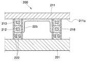
도 5a는 본 발명에 의한 플라즈마 디스플레이 패널의 제1 기판(211) 및 제2 기판(221)을 접합시키는 과정에서 발생된 소결 불량(290)을 설명하는 도면이다. 제1 기판(211) 상에는 다수 개의 방전셀(200)들이 형성된다. 형성된 방전셀(200)들은 봉함제(250)에 의하여 제2 기판(221)에 단단히 접착된다. 제2 기판(221)은 단순한 기판으로서 뿐만 아니라, 하부 샤시로서 동작할 수 있음은 전술된 바와 같다.5A is a diagram illustrating a
도 5a에 도시된 바와 같은 무하판 구조의 플라즈마 디스플레이 패널에서는, 제2 기판(221)은 종래 기술과 달리 유리 재질이 아닌 재질로 형성된다. 그런데, 제2 기판을 형성하는 재질은 유리 재질에 비하여 봉함시 봉함제와의 소결 효과가 저하된다. 그러므로, 기존의 봉함제를 이용할 경우 제1 기판(211) 및 제2 기판(221)이 완벽하게 봉함되지 않는 소결 불량(290)이 발생될 수 있다. 소결 불량(290)이 발생되면 고진공 상태인 플라즈마 디스플레이 패널 내부에 가스가 유입되므로 플라즈마 디스플레이 패널이 오동작할 수 있고, 이러한 소결 불량에 기인하여 생산 수율이 저하된다.In the plasma display panel having a plateless structure as shown in FIG. 5A, the
도 5b는 본 발명에 의한 플라즈마 디스플레이 패널의 다른 실시예를 나타내는 도면이다. 도 5b에 도시된 플라즈마 디스플레이 패널은 제1 기판(211) 및 제2 기판(221) 사이에 형성된 방전셀(200)을 포함한다. 다수 개의 방전셀(200)들은 봉함제(250)를 이용하여 단단히 봉함된다. 또한, 배기관(270)이 내부 공기를 외부로 환기한다.5B is a view showing another embodiment of a plasma display panel according to the present invention. The plasma display panel illustrated in FIG. 5B includes a
도 5b에 도시된 바와 같이, 본 발명은 제2 기판 및 봉함제(250) 간의 소결 특성을 개선시키기 위한 제1 버퍼층(285)을 포함한다. 제1 버퍼층(285)은 입자의 평균 입경이 작고 입도 분포가 조밀한 물질인 것이 바람직하다. 제1 버퍼층(285)에 의하여, 봉함제(250) 및 제2 기판(221)간의 소결 특성이 개선된다. 그러므로 생산 수율이 향상된다.As shown in FIG. 5B, the present invention includes a
또한, 본 발명은 봉함제(250) 및 제1 기판(211) 간의 소결 특성을 개선하는 제2 버퍼층(280)도 포함할 수 있다.In addition, the present invention may also include a
제1 및 제2 버퍼층은 플라즈마 디스플레이 패널 제조 공정에서 사용되는 유전체를 이용하여 생성될 수 있다. 유전체는 입자의 평균 입경이 0.5 내지 2.5 마이크로미터로서 치밀하고 소결 특성이 우수하므로 제2 기판(221) 및 봉함제(250) 간의 소결 특성을 보완하는데 바람직하다.The first and second buffer layers may be generated using dielectrics used in a plasma display panel manufacturing process. Since the dielectric has an average particle diameter of 0.5 to 2.5 micrometers and is dense and has excellent sintering characteristics, it is preferable to supplement the sintering characteristics between the
이하, 도 5a 및 도 5b를 이용하여 본 발명의 다른 측면에 의한 플라즈마 디스플레이 패널 제조 방법을 설명한다. 본원 발명에 의한 플라즈마 디스플레이 패널 제조 방법은 방전셀(200)을 제1 기판(211) 상에 형성하고, 제1 기판(211)을 제2 기판(221)에 접착하기 전에 제1 및 제2 버퍼층(285)을 형성하는 단계를 포함하는 것을 특징으로 한다. 제1 및 제2 버퍼층(280, 285)을 형성하고, 그 사이에 봉함제(250)를 부착시킴으로써 제1 및 제2 기판(211, 221)을 견실하게 접착할 수 있다.Hereinafter, a method of manufacturing a plasma display panel according to another aspect of the present invention will be described with reference to FIGS. 5A and 5B. In the plasma display panel manufacturing method according to the present invention, the
본 발명에 따른 플라즈마 디스플레이 패널은 다음과 같은 효과를 가진다.The plasma display panel according to the present invention has the following effects.
첫째, 본 발명에 의하여 발광 효율이 개선된 플라즈마 디스플레이 패널의 제1 및 제2 기판간 소결 불량을 방지함으로써 생산 수율을 향상시킬 수 있다.First, the present invention can improve the production yield by preventing sintering failure between the first and second substrates of the plasma display panel having improved luminous efficiency.
둘째, 발광셀에서 발광된 가시광선이 제1 기판을 통과하게 되는데, 가시광선 이 통과하는 제1 기판의 부분에는 전극들이 존재하지 않으므로, 개구율이 획기적으로 향상될 수 있고, 투과율이 향상된다.Second, the visible light emitted from the light emitting cell passes through the first substrate. Since the electrodes do not exist in the portion of the first substrate through which the visible light passes, the aperture ratio can be significantly improved, and the transmittance is improved.
셋째, 면 방전이 방전공간을 형성하는 모든 측면에서 발생될 수 있으므로, 방전면이 크게 확대될 수 있다.Third, since the surface discharge can be generated in all aspects forming the discharge space, the discharge surface can be greatly enlarged.
넷째, 방전이 발광셀을 형성하는 측면에서 발생하여 발광셀의 중앙부로 확산되므로, 방전영역이 종래에 비해 현저하게 향상됨으로써 발광셀 전체를 효율적으로 이용할 수 있다. 따라서, 낮은 전압으로도 구동이 가능하게 되어 발광효율을 획기적으로 향상시킬 수 있다.Fourth, since the discharge is generated on the side of forming the light emitting cell and diffused to the center portion of the light emitting cell, the discharge area is remarkably improved compared with the conventional one, so that the entire light emitting cell can be efficiently used. Therefore, the driving can be performed even at a low voltage, thereby significantly improving the luminous efficiency.
다섯째, 본 발명의 플라즈마 디스플레이 패널 및 이를 구비한 평판 표시 장치에서는 전술한 바와 같이 저 전압 구동이 가능하므로, 고농도 Xe 가스를 방전가스로 사용하더라도 저 전압 구동이 가능하게 되어 발광효율을 향상시킬 수 있다.Fifth, since the plasma display panel and the flat panel display device having the same according to the present invention can be driven at a low voltage as described above, even when a high concentration of Xe gas is used as the discharge gas, a low voltage can be driven to improve luminous efficiency. .
본 발명은 도면에 도시된 실시예를 참고로 설명되었으나 이는 예시적인 것에 불과하며, 본 기술 분야의 통상의 지식을 가진 자라면 이로부터 다양한 변형 및 균등한 다른 실시예가 가능하다는 점을 이해할 것이다. 따라서, 본 발명의 진정한 기술적 보호 범위는 첨부된 특허청구범위의 기술적 사상에 의하여 정해져야 할 것이다.Although the present invention has been described with reference to the embodiments shown in the drawings, this is merely exemplary, and it will be understood by those skilled in the art that various modifications and equivalent other embodiments are possible. Therefore, the true technical protection scope of the present invention will be defined by the technical spirit of the appended claims.
Claims (20)
Translated fromKoreanPriority Applications (1)
| Application Number | Priority Date | Filing Date | Title |
|---|---|---|---|
| KR1020050010965AKR100759552B1 (en) | 2005-02-05 | 2005-02-05 | Plasma Display Panel And Manufacturing Method |
Applications Claiming Priority (1)
| Application Number | Priority Date | Filing Date | Title |
|---|---|---|---|
| KR1020050010965AKR100759552B1 (en) | 2005-02-05 | 2005-02-05 | Plasma Display Panel And Manufacturing Method |
Publications (2)
| Publication Number | Publication Date |
|---|---|
| KR20060090434A KR20060090434A (en) | 2006-08-11 |
| KR100759552B1true KR100759552B1 (en) | 2007-09-18 |
Family
ID=37571637
Family Applications (1)
| Application Number | Title | Priority Date | Filing Date |
|---|---|---|---|
| KR1020050010965AExpired - Fee RelatedKR100759552B1 (en) | 2005-02-05 | 2005-02-05 | Plasma Display Panel And Manufacturing Method |
Country Status (1)
| Country | Link |
|---|---|
| KR (1) | KR100759552B1 (en) |
Citations (1)
| Publication number | Priority date | Publication date | Assignee | Title |
|---|---|---|---|---|
| JP2001189136A (en)* | 1999-10-19 | 2001-07-10 | Matsushita Electric Ind Co Ltd | Plasma display device and manufacturing method thereof |
- 2005
- 2005-02-05KRKR1020050010965Apatent/KR100759552B1/ennot_activeExpired - Fee Related
Patent Citations (1)
| Publication number | Priority date | Publication date | Assignee | Title |
|---|---|---|---|---|
| JP2001189136A (en)* | 1999-10-19 | 2001-07-10 | Matsushita Electric Ind Co Ltd | Plasma display device and manufacturing method thereof |
Also Published As
| Publication number | Publication date |
|---|---|
| KR20060090434A (en) | 2006-08-11 |
Similar Documents
| Publication | Publication Date | Title |
|---|---|---|
| KR100922745B1 (en) | Plasma display panel | |
| KR100581907B1 (en) | Plasma display panel | |
| KR100759552B1 (en) | Plasma Display Panel And Manufacturing Method | |
| KR100708660B1 (en) | Plasma Display Panel with Improved Contrast | |
| KR100751369B1 (en) | Plasma display panel | |
| KR100670281B1 (en) | Plasma display panel | |
| KR100592313B1 (en) | Plasma display panel | |
| KR100647647B1 (en) | Plasma display panel | |
| KR100708661B1 (en) | Plasma Display Panel with Improved Brightness | |
| KR100708664B1 (en) | Plasma display panel | |
| KR100647643B1 (en) | Plasma display panel | |
| KR100603412B1 (en) | Plasma display panel | |
| KR100647646B1 (en) | Plasma display panel | |
| KR100647655B1 (en) | Plasma display panel | |
| KR20050111173A (en) | Plasma display panel and method for manufacturing the same | |
| KR100670315B1 (en) | Plasma display panel | |
| KR100626064B1 (en) | Plasma display panel | |
| KR100719544B1 (en) | Plasma display panel | |
| KR100615310B1 (en) | Plasma display panel | |
| KR100581958B1 (en) | Plasma display panel | |
| KR100768211B1 (en) | Plasma Display Panel And Plasma Display Device Having The Same | |
| KR100708747B1 (en) | Plasma Display Panel And Plasma Display Device Having The Same | |
| KR20050105697A (en) | Plasma display panel | |
| KR20050105698A (en) | Plasma display panel | |
| KR20050104187A (en) | Plasma display panel |
Legal Events
| Date | Code | Title | Description |
|---|---|---|---|
| A201 | Request for examination | ||
| PA0109 | Patent application | St.27 status event code:A-0-1-A10-A12-nap-PA0109 | |
| PA0201 | Request for examination | St.27 status event code:A-1-2-D10-D11-exm-PA0201 | |
| R17-X000 | Change to representative recorded | St.27 status event code:A-3-3-R10-R17-oth-X000 | |
| PG1501 | Laying open of application | St.27 status event code:A-1-1-Q10-Q12-nap-PG1501 | |
| E902 | Notification of reason for refusal | ||
| PE0902 | Notice of grounds for rejection | St.27 status event code:A-1-2-D10-D21-exm-PE0902 | |
| P11-X000 | Amendment of application requested | St.27 status event code:A-2-2-P10-P11-nap-X000 | |
| P13-X000 | Application amended | St.27 status event code:A-2-2-P10-P13-nap-X000 | |
| E701 | Decision to grant or registration of patent right | ||
| PE0701 | Decision of registration | St.27 status event code:A-1-2-D10-D22-exm-PE0701 | |
| GRNT | Written decision to grant | ||
| PR0701 | Registration of establishment | St.27 status event code:A-2-4-F10-F11-exm-PR0701 | |
| PR1002 | Payment of registration fee | St.27 status event code:A-2-2-U10-U11-oth-PR1002 Fee payment year number:1 | |
| PG1601 | Publication of registration | St.27 status event code:A-4-4-Q10-Q13-nap-PG1601 | |
| G170 | Re-publication after modification of scope of protection [patent] | ||
| PG1701 | Publication of correction | St.27 status event code:A-5-5-P10-P19-oth-PG1701 Patent document republication publication date:20080417 Republication note text:Request for Correction Notice (Document Request) Gazette number:1007595520000 Gazette reference publication date:20070918 | |
| R18-X000 | Changes to party contact information recorded | St.27 status event code:A-5-5-R10-R18-oth-X000 | |
| R18-X000 | Changes to party contact information recorded | St.27 status event code:A-5-5-R10-R18-oth-X000 | |
| LAPS | Lapse due to unpaid annual fee | ||
| PC1903 | Unpaid annual fee | St.27 status event code:A-4-4-U10-U13-oth-PC1903 Not in force date:20100912 Payment event data comment text:Termination Category : DEFAULT_OF_REGISTRATION_FEE | |
| PC1903 | Unpaid annual fee | St.27 status event code:N-4-6-H10-H13-oth-PC1903 Ip right cessation event data comment text:Termination Category : DEFAULT_OF_REGISTRATION_FEE Not in force date:20100912 | |
| P22-X000 | Classification modified | St.27 status event code:A-4-4-P10-P22-nap-X000 | |
| R18-X000 | Changes to party contact information recorded | St.27 status event code:A-5-5-R10-R18-oth-X000 | |
| P22-X000 | Classification modified | St.27 status event code:A-4-4-P10-P22-nap-X000 | |
| R18-X000 | Changes to party contact information recorded | St.27 status event code:A-5-5-R10-R18-oth-X000 |