KR100754844B1 - RF ID Tag - Google Patents
RF ID TagDownload PDFInfo
- Publication number
- KR100754844B1 KR100754844B1KR1020060046738AKR20060046738AKR100754844B1KR 100754844 B1KR100754844 B1KR 100754844B1KR 1020060046738 AKR1020060046738 AKR 1020060046738AKR 20060046738 AKR20060046738 AKR 20060046738AKR 100754844 B1KR100754844 B1KR 100754844B1
- Authority
- KR
- South Korea
- Prior art keywords
- slot
- tag
- conductor plate
- rfid
- chip
- Prior art date
- Legal status (The legal status is an assumption and is not a legal conclusion. Google has not performed a legal analysis and makes no representation as to the accuracy of the status listed.)
- Expired - Fee Related
Links
Images


Classifications
- G—PHYSICS
- G06—COMPUTING OR CALCULATING; COUNTING
- G06K—GRAPHICAL DATA READING; PRESENTATION OF DATA; RECORD CARRIERS; HANDLING RECORD CARRIERS
- G06K19/00—Record carriers for use with machines and with at least a part designed to carry digital markings
- G06K19/06—Record carriers for use with machines and with at least a part designed to carry digital markings characterised by the kind of the digital marking, e.g. shape, nature, code
- G06K19/067—Record carriers with conductive marks, printed circuits or semiconductor circuit elements, e.g. credit or identity cards also with resonating or responding marks without active components
- G06K19/07—Record carriers with conductive marks, printed circuits or semiconductor circuit elements, e.g. credit or identity cards also with resonating or responding marks without active components with integrated circuit chips
- G06K19/077—Constructional details, e.g. mounting of circuits in the carrier
- G06K19/07749—Constructional details, e.g. mounting of circuits in the carrier the record carrier being capable of non-contact communication, e.g. constructional details of the antenna of a non-contact smart card
- G—PHYSICS
- G06—COMPUTING OR CALCULATING; COUNTING
- G06K—GRAPHICAL DATA READING; PRESENTATION OF DATA; RECORD CARRIERS; HANDLING RECORD CARRIERS
- G06K19/00—Record carriers for use with machines and with at least a part designed to carry digital markings
- G06K19/06—Record carriers for use with machines and with at least a part designed to carry digital markings characterised by the kind of the digital marking, e.g. shape, nature, code
- G06K19/067—Record carriers with conductive marks, printed circuits or semiconductor circuit elements, e.g. credit or identity cards also with resonating or responding marks without active components
- G06K19/07—Record carriers with conductive marks, printed circuits or semiconductor circuit elements, e.g. credit or identity cards also with resonating or responding marks without active components with integrated circuit chips
- G06K19/077—Constructional details, e.g. mounting of circuits in the carrier
- G06K19/07745—Mounting details of integrated circuit chips
- Y—GENERAL TAGGING OF NEW TECHNOLOGICAL DEVELOPMENTS; GENERAL TAGGING OF CROSS-SECTIONAL TECHNOLOGIES SPANNING OVER SEVERAL SECTIONS OF THE IPC; TECHNICAL SUBJECTS COVERED BY FORMER USPC CROSS-REFERENCE ART COLLECTIONS [XRACs] AND DIGESTS
- Y10—TECHNICAL SUBJECTS COVERED BY FORMER USPC
- Y10S—TECHNICAL SUBJECTS COVERED BY FORMER USPC CROSS-REFERENCE ART COLLECTIONS [XRACs] AND DIGESTS
- Y10S264/00—Plastic and nonmetallic article shaping or treating: processes
- Y10S264/10—Foamed polystyrene mold filling
Landscapes
- Engineering & Computer Science (AREA)
- Computer Hardware Design (AREA)
- Microelectronics & Electronic Packaging (AREA)
- Physics & Mathematics (AREA)
- General Physics & Mathematics (AREA)
- Theoretical Computer Science (AREA)
- Waveguide Aerials (AREA)
Abstract
Description
Translated fromKorean도 1은 본 발명의 실시예에 의한 알에프 아이디 태그를 보인 사시도1 is a perspective view showing an RFID tag according to an embodiment of the present invention
도 2는 본 발명의 실시예에 의한 알에프 아이디 태그를 보인 측면도Figure 2 is a side view showing the RFID ID tag according to an embodiment of the present invention
도 3은 본 발명의 실시예에 의한 알에프 아이디 태그를 보인 평면도3 is a plan view showing an RFID tag according to an embodiment of the present invention
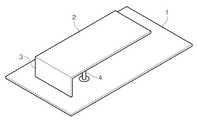
도 4는 종래의 알에프 아이디의 안테나를 설명하기 위한 도면4 is a view for explaining the antenna of the conventional RFID ID
<부호의 간단한 설명><Short description of symbols>
10 상부 도체판11 제1슬롯10
12 제2슬롯13 제3슬롯12
20 알에프 아이디 태그 칩30 연결 도체20 RF
40 유전체50 접지 도체판40 dielectric 50 grounding conductor plate
100 알에프 아이디 태그100RF ID Tag
본 발명은 알에프 아이디 태그에 관한 것으로서, 더 상세하게는 고유전율을 갖는 피 부착물 또는 도체인 피 부착물에 부착하여도 동작가능한 수동형 알에프 아이디 태그에 관한 것이다.The present invention relates to an RFID ID tag, and more particularly, to a passive RFID ID tag that is operable even when attached to an adherend to be attached or a conductor to be attached having a high dielectric constant.
최근, 전파를 이용함으로써 비접촉으로 판독기/기록기(reader/writer) 등의 외부 기기로부터 전력 공급 및 정보를 받아 상기 외부 기기로 정보를 송출하는 비접촉 IC 카드 등의 RFID 태그가 제공되어 있다. 이 RFID 태그는 플라스틱이나 종이 등의 기재에 설치한 송수신용 안테나 패턴과 IC 칩으로 이루어지고, 상기 안테나 패턴과 상기 IC 칩에 내장된 용량 소자에 의해 공진 회로를 형성하며, 상기 안테나 패턴을 통하여 무선으로 외부 기기와 교신할 수 있도록 구성되어 있다.In recent years, RFID tags, such as a non-contact IC card, which receive power supply and information from an external device such as a reader / writer and transmit information to the external device by contactlessly by using radio waves, have been provided. The RFID tag is composed of an antenna pattern for transmitting and receiving and an IC chip installed on a substrate such as plastic or paper, and a resonance circuit is formed by the antenna pattern and a capacitive element embedded in the IC chip. It is configured to communicate with external device.
기존의 상품의 종류 및 가격등의 정보를 기록하는 방식 중에 하나인 바코드와 마찬가지로 상기 태그의 칩에는 각 상품의 고유 정보가 기록되어 있다. 리더에서 송신한 신호가 태그에 입력되면, 태그는 칩에 기록된 정보를 태그 안테나를 통해 다시 리더로 송신하게 된다. 따라서, 상기 태그 안테나는 소형 또는 컴팩트한 사이즈이어야 하며, 리더에서 출력한 신호를 입력받아 태그의 동작전원으로 사용해야 하며, 태그의 칩에 기록된 정보를 다시 리더로 송신해야 함으로서 안테나의 기능이 우수해야 한다.As with a bar code, which is one of the existing methods of recording information such as the type and price of goods, the unique information of each product is recorded on the chip of the tag. When the signal transmitted from the reader is input to the tag, the tag transmits the information recorded on the chip to the reader through the tag antenna. Therefore, the tag antenna should be small or compact in size, should receive the signal output from the reader and use it as the operating power of the tag, and transmit the information recorded on the chip of the tag back to the reader. do.
상기와 같은 RFID 태그는 예를 들면 물이나 와인이 들어있는 병, 인체, 도체로 만든 캔 등의 높은 유전율 또는 도전율을 갖는 물체에 근접하여 사용되는 경우가 있다. 이러한 물체위에 태그가 부착되면 태그 안테나 양단에 필요한 전압이 형성되지 않아 통신에 악영향을 미치게 된다.Such an RFID tag may be used in close proximity to an object having high dielectric constant or conductivity, such as a bottle containing water or wine, a human body, a can made of a conductor, and the like. If a tag is attached to such an object, a voltage required across the tag antenna is not formed, which adversely affects communication.
UHF 대역에서 현재까지 개발된 RFID 태그 안테나는 주로 다이폴 안테나 형태나 이에서 약간 변형된 형태를 가지고 있다. 수동형 RFID 시스템에 할당된 911MHz의 중심 주파수에서 한 파장의 길이는 33cm 정도로 반 파장 다이폴 안테나의 경우 16cm 정도가 되며 구불거리는 형태를 사용할 시 보통 13cm 정도까지 그 길이를 줄일 수 있다. 이러한 태그 안테나는 유전율이 낮은 일반적 상품에 부착하였을 때 정상적으로 작동하나 고유전율을 가지는 물병이나 고도전율을 가지는 금속 표면 (예: 통조림 캔 표면 등) 상에 부착할 때는 불가능하다. 이는 도체 표면에 부착 시 다이폴 안테나의 두 터미널 사이가 단락이 되어 태그를 구동하기 위한 필요 전압차가 발생할 수 없기 때문이다. 이러한 다이폴 태그 안테나가 적절히 작동하기 위해서는 금속 표면에서 일정 간격 이격(약 파장의 1/4)되어야 하는데, 이러할 경우 태그 안테나가 차지하는 공간이 너무 커지는 단점을 갖게 된다. 이러한 문제를 해결하기 위하여 다이폴 형태의 안테나를 금속 표면에서 일정거리(1-2cm)를 띄워서 사용하는 태그 안테나가 출시되었는데, 상기 두 터미널 간의 이격 거리가 충분하지 않아 그 특성이 크게 제한된다. 따라서, 도 4에 도시된 바와 같이 도체 위에 부착할 수 있는 안테나로 Planar Inverted-F Antenna를 고려해 볼 수 있으나 이 안테나의 급전 구조는 보통 도 4에서 보는 것과 같이 상판(2)과 접지판(1)이 일정간격 이격되어 외부의 전파에 의해 전위차가 발생하여 급전라인(4)에 의해 알에프 아이디 칩(미도시)에 전원공급이 가능하나, 상기 급전라인(4)이 수직 형태로 되어 있어 알에프 아이디 칩을 부착하기가 용이하지 않는 단점이 있다.RFID tag antennas developed to date in the UHF band mainly have a dipole antenna shape or a slight variation thereof. At the center frequency of 911 MHz, which is assigned to passive RFID systems, one wavelength is about 33cm long and about 16cm for half-wave dipole antennas. These tag antennas work normally when attached to common products with low dielectric constants, but not on water bottles with high dielectric constants or metal surfaces with high dielectric constants (eg canned can surfaces). This is because when attached to the conductor surface, there is a short circuit between the two terminals of the dipole antenna, so that the required voltage difference for driving the tag cannot occur. In order for the dipole tag antenna to function properly, the dipole tag antenna must be spaced apart (about 1/4 of a wavelength) from the metal surface, which causes a disadvantage that the space occupied by the tag antenna becomes too large. In order to solve this problem, a tag antenna using a dipole-shaped antenna with a predetermined distance (1-2 cm) away from a metal surface has been released. However, since the separation distance between the two terminals is not sufficient, its characteristics are greatly limited. Therefore, as shown in FIG. 4, a planar inverted-F antenna may be considered as an antenna that can be attached to a conductor, but the feeding structure of the antenna is generally the top plate 2 and the ground plate 1 as shown in FIG. 4. The electric potential difference is generated by the electric wave from the outside spaced apart at regular intervals, and the power supply line 4 can supply power to the RF ID chip (not shown), but the power supply line 4 has a vertical shape, and thus the ID ID chip. There is a disadvantage that is not easy to attach.
본 발명은 상기와 같은 문제점을 해결하기 위해 안출된 것으로, 알에프 아이디 칩의 설치가 용이하고, UHF 대역에서 피 부착물이 도체인 경우에도 부착하여 동작가능한 알에프 아이디 태그를 제공하는 것을 목적으로 한다.The present invention has been made to solve the above problems, and an object of the present invention is to provide an RFID ID tag that is easy to install an RFID ID chip and that can be attached and operated even when the object is a conductor in the UHF band.
상기와 같은 목적을 달성하기 위한 본 발명의 알에프 아이디 태그는 접지 도체판과, 상기 접지 도체판으로 부터 일정간격 이격되어 배치되고, 제1슬롯과 제2슬롯과 상기 제1슬롯과 제2슬롯을 연결하는 제3슬롯이 형성된 상부 도체판과, 상기 제3슬롯을 가로질러 배치된 알에프 아이디 칩과, 상기 상부 도체판과 상기 접지 도체판을 연결하는 연결도체를 포함하는 것을 특징으로 한다.RF ID tag of the present invention for achieving the above object is disposed at a predetermined distance from the ground conductor plate, the ground conductor plate, the first slot and the second slot and the first slot and the second slot And an upper conductor plate on which a third slot to connect is formed, an RF ID chip disposed across the third slot, and a connection conductor connecting the upper conductor plate and the ground conductor plate.
또한, 본 발명의 알에프 아이디 태그는 상기 접지 도체판과 상기 상부 도체판 사이에 유전체를 더 포함하는데, 이때 이 유전체의 상대 유전율을 낮은 것으로 사용할 수도 또 높은 것을 사용할 수도 있다, 낮은 상대 유전율을 사용하면 태그 안테나의 크기가 커지지만 안테나의 이득이 높아져 인식거리도 길어지게 된다. 높은 상대 유전율을 사용할 경우 안테나의 크기를 줄일 수 있지만 안테나 이득이 작아져 인식거리가 짧아진다. 요구되는 인식거리에 따라 적절한 유전율을 선택할 수 있다.In addition, the RFID ID tag of the present invention further includes a dielectric between the ground conductor plate and the upper conductor plate, wherein the relative permittivity of the dielectric may be used as a low or high one. Although the size of the tag antenna increases, the gain of the antenna increases, so that the recognition distance also increases. The use of a high relative permittivity can reduce the size of the antenna, but the antenna gain is smaller, resulting in a shorter recognition distance. The proper permittivity can be selected according to the recognition distance required.
또한, 본 발명의 알에프 아이디 태그는 상기 상부 도체판의 일단이 절곡되어 상기 유전체의 내부에 삽입된 것을 특징으로 한다.In addition, the RFID tag of the present invention is characterized in that one end of the upper conductor plate is bent and inserted into the dielectric.
상기와 같이 상기 상부 도체판과 접지 도체판이 일정간격 이격된 구조이므로, 그 형태 변형을 방지하고자 접지 도체판과 상부 도체판의 사이에는 유전체를 삽입한다. 이때 유전체에 의한 전기적 영향을 최소화 하기 위하여 공기의 유전율과 유사한 재질의 유전체를 삽입해야 하는데, 발포 스티렌 수지를 삽입함이 가장 바람직 하다.Since the upper conductor plate and the ground conductor plate are spaced apart from each other as described above, a dielectric is inserted between the ground conductor plate and the upper conductor plate to prevent deformation of the shape. At this time, in order to minimize the electrical influence by the dielectric, it is necessary to insert a dielectric material similar to the dielectric constant of the air, it is most preferable to insert the foamed styrene resin.
또한, 본 발명의 알에프 아이디 태그에서 상기 제1슬롯과 제2슬롯은 각각 동일하게 설정된 폭과 길이를 갖고 설정 간격으로 평행하게 배치되되, 각각의 제1슬롯과 제2슬롯의 폭과 배치간격은 상기 상부 도체판의 임피던스 값이 상기 알에프 아이디 칩의 임피던스 값과 공액정합을 이루도록 설정된 것을 특징으로 한다.In addition, in the RFID ID tag of the present invention, the first slot and the second slot have the same width and length, respectively, are arranged in parallel at a predetermined interval, the width and the spacing of each of the first slot and the second slot The impedance value of the upper conductor plate is set to achieve a conjugate matching with the impedance value of the RFID chip.
통상의 기 제작된 알에프 아이디 칩의 임피던스 값이 보통 용량성 부하를 갖는 것을 감안하여 상기 알에프 아이디 칩의 임피던스 값과 공액정합을 이루도록 상부 도체판의 임피던스 값은 유도성 부하를 갖도록 해야 한다. 따라서, 상기 상부 도체판의 제1 및 제2 슬롯의 폭과 배치간격을 조절하여 상부 도체판의 임피던스 값이 상기 알에프 아이디 칩의 임피던스 값과 공액정합을 이루도록 설정한다.Given that the impedance value of the conventional RFID ID chip manufactured in general has a capacitive load, the impedance value of the upper conductor plate should have an inductive load so as to achieve a conjugate matching with the impedance value of the RFID ID chip. Accordingly, the width of the first and second slots of the upper conductor plate and the spacing between the slots are adjusted so that the impedance value of the upper conductor plate is conjugated with the impedance value of the RFID chip.
또한, 본 발명의 알에프 아이디 태그에서 상기 제3슬롯은 상기 제1슬롯과 제2슬롯의 마주 보는 단부를 연결하는 것을 특징으로 한다.In addition, the third slot in the RFID tag of the present invention is characterized in that connecting the opposite end of the first slot and the second slot.
이하에서는 첨부된 도면을 참조하여 본 발명의 알에프 아이디 태그의 실시예에 대하여 상세히 설명한다.Hereinafter, with reference to the accompanying drawings will be described in detail an embodiment of the RFID ID tag of the present invention.
도 1은 본 발명의 실시예에 의한 알에프 아이디 태그를 보인 사시도이고, 도 2는 본 발명의 실시예에 의한 알에프 아이디 태그를 보인 측면도이며, 도 3은 본 발명의 실시예에 의한 알에프 아이디 태그를 보인 평면도이다.1 is a perspective view showing an RFID ID tag according to an embodiment of the present invention, Figure 2 is a side view showing an RFID ID tag according to an embodiment of the present invention, Figure 3 is an ID tag according to an embodiment of the present invention It is the top view shown.
먼저, 도 1을 참조하여 본 실시예에 의한 알에프 아이디 태그의 구조를 살펴보면 다음과 같다.First, referring to FIG. 1, the structure of the RF ID tag according to the present embodiment is as follows.
본 실시예의 알에프 아이디 태그(100)는 사각 판 형태의 접지 도체판(50)과, 상기 접지 도체판(50)의 상면으로부터 상부방향으로 일정간격 이격되어 배치되고, 동일하게 설정된 폭(Sw)과 길이를 갖고 설정 간격(d)으로 평행하게 배치된 제1슬롯(11)과 제2슬롯(12)과, 상기 제1슬롯(11)과 제2슬롯(12)의 마주보는 단부를 연결하는 제3슬롯(13)이 형성된 상부 도체판(10)과, 상기 제3슬롯(13)을 가로질러 제3슬롯(13)을 기준으로 일측과 타측에 전기적으로 연결된 알에프 아이디 칩(20)과, 상기 상부 도체판(10)과 상기 접지 도체판(50)을 연결하는 연결도체(30)를 포함한다. 본 실시예의 상부 도체판(10)의 외부의 전파를 입력받고, 칩의 출력신호를 송신하는 안테나의 역할을 담당한다.The
상기 상부 도체판(10)의 일측단부, 즉 상기 제3슬롯(13)이 형성된 측의 타측단부는 절곡되어 도 2에 도시된 바와 같이 'ㄷ'의 형태를 보이는데, 이는 안테나적인 특성을 유지토록 하면서 알에프 아이디 태그의 사이즈를 줄이기 위함이다. 또한, 상기 접지 도체판(10)과 접지 도체판(50)의 사이에는 상부 도체판(10)과 접지 도체판(50)이 일정간격 이격된 구조이므로, 그 형태 변형을 방지하고자 접지 도체판(50)과 상부 도체판(10)의 사이에는 유전체(40)가 더 삽입된다. 이때 유전체(40)에 의한 전기적 영향을 최소화 하기 위하여 공기의 유전율과 유사한 재질의 유전체를 삽입해야 하는데, 발포 스티렌 수지를 삽입함이 가장 바람직 하다. 상기 발포 스티렌 수지는 그 유전율이 공기와 실질적으로 거의 동일하며, 가격이 저렴하여 제조원가의 절감효과가 있다. 본 실시예에서는 상기 유전체를 발포 스티렌 수지로 함을 예로 하여 설명하나 이에 한정되는 것은 아니다.One end of the
따라서, 상기 상부 도체판(10)의 절곡된 부분은 상기 유전체(40)에 삽입되며, 상기 유전체(40)에 의해 상부 도체판(10)의 형태변형, 즉 찌그러짐등이 방지된 다.Therefore, the bent portion of the
통상의 수동형 알에프 아이디 태그는 별도의 전원이 구비되어 있지 않아서, 리더가 송출한 전파를 상기 상부 도체판(10)으로 입력받아, 알에프 아이디 칩 내부의 정류 및 체배 회로를 이용하여 칩의 구동 전원을 발생한다. 상기 알에프 아이디 칩을 정상적으로 구동시키기 위해서는 알에프 아이디 태그가 배치된 위치에서 리더로부터 송출된 전파의 세기가 특정 값 이상이 되어야 함으로, RFID 태그는 소형, 경량, 저가로 만들면서도 최대의 효율을 갖는 안테나 부재가 필수적이다. 따라서, 알에프 아이디 태그의 안테나 효율을 상승시키기 위해서는 알에프 아이디 칩의 임피던스값과 안테나 부재의 임피던스가 상호 공액 정합(conjugate match) 되었을 때, 리더로부터 수신한 전력이 태그 칩에 최대로 전달될 수 있다.Since the conventional passive ID tag does not have a separate power source, a radio wave transmitted by the reader is inputted to the
상기 알에프 아이디 칩의 임피던스 값은 미리 결정되는 것이므로, 상기 알에프 아이디 태그의 안테나 부재의 임피던스 값을 조절하여 상기 알에프 아이디 칩의 임피던스 값과 공액정합을 이루도록 해야 한다. 본 실시예의 알에프 아이디 태그에서 안테나 부재, 즉 상부 도체판(10)의 임피던스 값 조절은 상기 제1슬롯(11)과 제2슬롯(12)의 폭(Sw)과 상호 배치간격(d)을 조절하여 달성된다.Since the impedance value of the RFID chip is determined in advance, the impedance value of the antenna member of the RFID tag must be adjusted to achieve a conjugate match with the impedance of the RFID chip. In the RFID ID tag according to the present embodiment, the impedance value of the antenna member, that is, the
아래 참고도 1은 각각의 제1슬롯(11)과 제2슬롯(12)의 폭의 길이를 변화시켜 측정한 상부 도체판(10)의 저항값의 변화 그래프이며, 참고도 2는 각각의 제1슬롯(11)과 제2슬롯(12)의 상호 배치간격(d)을 변화시켜 측정한 상부 도체판(10)의 리액턴스 값의 변화 그래프 이다.Reference 1 below is a graph of the change in the resistance value of the
[참고도 1][Reference Figure 1]

[참고도 2][Reference Figure 2]

통상의 기 제작된 알에프 아이디 칩의 임피던스 값이 보통 용량성 부하(임피던스의 허수부가 음)를 갖는 것을 감안하여 상기 알에프 아이디 칩의 임피던스 값 과 공액정합을 이루도록 상부 도체판의 임피던스 값은 유도성 부하(임피던스의 허수부가 양)를 갖도록 해야 한다. 따라서, 상기 상부 도체판(10)의 제1 및 제2 슬롯(11,12)의 폭과 배치간격을 조절하여 상부 도체판(10)의 임피던스 값이 상기 알에프 아이디 칩의 임피던스 값과 공액정합을 이루도록 한다.The impedance value of the upper conductor plate is inductive load so that the impedance value of the conventional RFID chip has a common capacitive load (negative imaginary part of impedance) is negatively matched with the impedance value of the RFID chip. (The imaginary part of the impedance is positive). Therefore, the impedance value of the
본 실시예의 알에프 아이디 태그(100)는 접지 도체판(50)에 의해 금속성 재질의 피 부착물에 부착될 수 있다. 즉, 피 부착물의 표면이 도체이더라도, 각각의 재질에 따라 전기적인 성질이 각기 달라지므로 접지의 균일성이 떨어지는데, 본 실시예의 접지 도체판(50)을 별도로 구비하여 안정적인 접지성을 갖도록 한다. 또한, 상기의 접지 도체판(50)에 의해 유전율이 작은 피 부착물, 즉 비도체에 부착하여도 상기 접지 도체판(50)과 상부 도체판(10)의 전위차에 의해 알에프 아이디 칩에 필요한 전력을 공급할 수 있는 장점이 있다.
상기와 같은 본 발명의 알에프 아이디 태그는 피 부착물이 유전율이 작은 물품, 즉 비도체 뿐만 아니라 도체에도 부착하여 사용할 수 있어 사용 범용성이 향상된 장점이 있다.RF ID tag of the present invention as described above has the advantage that the object can be attached to the article having a small dielectric constant, that is, non-conductor as well as can be used to attach the conductor.
즉, Planar Inverted-F 타입 안테나를 사용하는 알에프 아이디 태그에서 알에프 아이디 칩이 설치되는 상부 도체판이 평면형이어서 제조 및 칩의 설치가 용이한 장점이 있다.That is, in the RFID ID tag using a Planar Inverted-F type antenna, the upper conductor plate on which the RFID ID chip is installed is flat, so that manufacturing and installation of the chip are easy.
또한, 기 제작되는 칩의 임피던스를 감안하여 상부 도체판의 임피던스를 슬롯의 폭 및 배치간격을 조절하여 결정할 수 있으므로, 다양한 알에프 아이디 칩에 대응하여 용이하게 안테나 부재를 설계할 수 있는 장점이 있다.In addition, since the impedance of the upper conductor plate may be determined by adjusting the width and the placement interval of the slot in consideration of the impedance of the manufactured chip, there is an advantage that the antenna member may be easily designed to cope with various RFID ID chips.
앞에서 설명되고, 도면에 도시된 본 발명의 일 실시예는 본 발명의 기술적 사상을 한정하는 것으로 해석되어서는 안 된다. 본 발명의 보호범위는 청구범위에 기재된 사항에 의하여만 제한되고, 본 발명의 기술분야에서 통상의 지식을 가진 자는 본 발명의 기술적 사상을 다양한 형태로 개량 변경하는 것이 가능하다. 따라서 이러한 개량 및 변경은 통상의 지식을 가진 자에게 자명한 것인 한 본 발명의 보호범위에 속하게 될 것이다.An embodiment of the present invention described above and illustrated in the drawings should not be construed as limiting the technical spirit of the present invention. The protection scope of the present invention is limited only by the matters described in the claims, and those skilled in the art can change and change the technical idea of the present invention in various forms. Therefore, such improvements and modifications will fall within the protection scope of the present invention, as will be apparent to those skilled in the art.
Claims (7)
Translated fromKoreanPriority Applications (1)
| Application Number | Priority Date | Filing Date | Title |
|---|---|---|---|
| KR1020060046738AKR100754844B1 (en) | 2006-05-24 | 2006-05-24 | RF ID Tag |
Applications Claiming Priority (1)
| Application Number | Priority Date | Filing Date | Title |
|---|---|---|---|
| KR1020060046738AKR100754844B1 (en) | 2006-05-24 | 2006-05-24 | RF ID Tag |
Publications (1)
| Publication Number | Publication Date |
|---|---|
| KR100754844B1true KR100754844B1 (en) | 2007-09-04 |
Family
ID=38736271
Family Applications (1)
| Application Number | Title | Priority Date | Filing Date |
|---|---|---|---|
| KR1020060046738AExpired - Fee RelatedKR100754844B1 (en) | 2006-05-24 | 2006-05-24 | RF ID Tag |
Country Status (1)
| Country | Link |
|---|---|
| KR (1) | KR100754844B1 (en) |
Citations (5)
| Publication number | Priority date | Publication date | Assignee | Title |
|---|---|---|---|---|
| JPH07221538A (en)* | 1994-01-31 | 1995-08-18 | Nippon Signal Co Ltd:The | Slot antenna system |
| KR960002828B1 (en)* | 1986-07-29 | 1996-02-26 | 암테크 코오퍼레이션 | Transponder antenna |
| US20020167450A1 (en) | 1999-11-18 | 2002-11-14 | Siemens Ag | Mobile data carrier including a transponder having a surface wave component and a slot antenna |
| JP2002358494A (en) | 2001-06-01 | 2002-12-13 | Hitachi Kokusai Electric Inc | Mobile object identification wireless tag |
| WO2005048181A1 (en) | 2003-11-04 | 2005-05-26 | Avery Dennison Corporation | Rfid tag with enhanced readability |
- 2006
- 2006-05-24KRKR1020060046738Apatent/KR100754844B1/ennot_activeExpired - Fee Related
Patent Citations (5)
| Publication number | Priority date | Publication date | Assignee | Title |
|---|---|---|---|---|
| KR960002828B1 (en)* | 1986-07-29 | 1996-02-26 | 암테크 코오퍼레이션 | Transponder antenna |
| JPH07221538A (en)* | 1994-01-31 | 1995-08-18 | Nippon Signal Co Ltd:The | Slot antenna system |
| US20020167450A1 (en) | 1999-11-18 | 2002-11-14 | Siemens Ag | Mobile data carrier including a transponder having a surface wave component and a slot antenna |
| JP2002358494A (en) | 2001-06-01 | 2002-12-13 | Hitachi Kokusai Electric Inc | Mobile object identification wireless tag |
| WO2005048181A1 (en) | 2003-11-04 | 2005-05-26 | Avery Dennison Corporation | Rfid tag with enhanced readability |
Similar Documents
| Publication | Publication Date | Title |
|---|---|---|
| EP2283539B1 (en) | Rfid tag | |
| EP2183709B1 (en) | Antenna systems for passive rfid tags | |
| EP1689031B1 (en) | Multi-band wireless communication device | |
| US7570225B2 (en) | Antenna and non-contact tag | |
| KR100839601B1 (en) | Antenna, RDF Tag and Antenna Impedance Matching Method Using Proximity Coupling with Short-Ended Feed Lines | |
| KR100820544B1 (en) | RDF tag and its antenna | |
| KR20140075021A (en) | Miniaturized radio-frequency identification tag and microstrip patch antenna thereof | |
| CN101842937A (en) | RFID antenna system and method | |
| EP2345983B1 (en) | Radio frequency identification tag | |
| CN107768832A (en) | RFID label tag and RFID label antenna | |
| CN201117802Y (en) | Ultra- wide-band electronic label antenna | |
| WO2000026993A1 (en) | Radio frequency tag with optimum power transfer | |
| CN201112565Y (en) | High-performance Yagi electronic label antenna | |
| KR100792345B1 (en) | Tag Antenna for RFID | |
| CN101901957A (en) | Micro radio frequency identification tag and micro strip patch antenna therein | |
| KR100688093B1 (en) | Antenna, RFD Tag, and Antenna Impedance Matching Method Using Proximity Coupled Feeding | |
| CN201117815Y (en) | Low cost broad band small volume high gain linear polarization antenna | |
| KR100754844B1 (en) | RF ID Tag | |
| KR100867853B1 (en) | RFID antennas and RDF tags | |
| KR100848560B1 (en) | Solid State Flat Antenna | |
| WO2007089106A1 (en) | Antenna using proximity-coupling between radiation patch and short-ended feed line, rfid tag employing the same, and antenna impedance matching method thereof | |
| FI130267B (en) | A uhf rfid tag | |
| CN201087909Y (en) | Electronic label antenna composed of words and letters | |
| KR100793525B1 (en) | RFID tag | |
| KR100820545B1 (en) | RFID antennas and RDF tags |
Legal Events
| Date | Code | Title | Description |
|---|---|---|---|
| A201 | Request for examination | ||
| PA0109 | Patent application | St.27 status event code:A-0-1-A10-A12-nap-PA0109 | |
| PA0201 | Request for examination | St.27 status event code:A-1-2-D10-D11-exm-PA0201 | |
| D13-X000 | Search requested | St.27 status event code:A-1-2-D10-D13-srh-X000 | |
| D14-X000 | Search report completed | St.27 status event code:A-1-2-D10-D14-srh-X000 | |
| R18-X000 | Changes to party contact information recorded | St.27 status event code:A-3-3-R10-R18-oth-X000 | |
| E701 | Decision to grant or registration of patent right | ||
| PE0701 | Decision of registration | St.27 status event code:A-1-2-D10-D22-exm-PE0701 | |
| GRNT | Written decision to grant | ||
| PR0701 | Registration of establishment | St.27 status event code:A-2-4-F10-F11-exm-PR0701 | |
| PR1002 | Payment of registration fee | St.27 status event code:A-2-2-U10-U11-oth-PR1002 Fee payment year number:1 | |
| PG1601 | Publication of registration | St.27 status event code:A-4-4-Q10-Q13-nap-PG1601 | |
| PN2301 | Change of applicant | St.27 status event code:A-5-5-R10-R13-asn-PN2301 St.27 status event code:A-5-5-R10-R11-asn-PN2301 | |
| R18-X000 | Changes to party contact information recorded | St.27 status event code:A-5-5-R10-R18-oth-X000 | |
| PR1001 | Payment of annual fee | St.27 status event code:A-4-4-U10-U11-oth-PR1001 Fee payment year number:4 | |
| FPAY | Annual fee payment | Payment date:20110803 Year of fee payment:5 | |
| PR1001 | Payment of annual fee | St.27 status event code:A-4-4-U10-U11-oth-PR1001 Fee payment year number:5 | |
| FPAY | Annual fee payment | Payment date:20120829 Year of fee payment:6 | |
| PR1001 | Payment of annual fee | St.27 status event code:A-4-4-U10-U11-oth-PR1001 Fee payment year number:6 | |
| LAPS | Lapse due to unpaid annual fee | ||
| PC1903 | Unpaid annual fee | St.27 status event code:A-4-4-U10-U13-oth-PC1903 Not in force date:20130829 Payment event data comment text:Termination Category : DEFAULT_OF_REGISTRATION_FEE | |
| PC1903 | Unpaid annual fee | St.27 status event code:N-4-6-H10-H13-oth-PC1903 Ip right cessation event data comment text:Termination Category : DEFAULT_OF_REGISTRATION_FEE Not in force date:20130829 | |
| R18-X000 | Changes to party contact information recorded | St.27 status event code:A-5-5-R10-R18-oth-X000 | |
| P22-X000 | Classification modified | St.27 status event code:A-4-4-P10-P22-nap-X000 | |
| P22-X000 | Classification modified | St.27 status event code:A-4-4-P10-P22-nap-X000 | |
| R18-X000 | Changes to party contact information recorded | St.27 status event code:A-5-5-R10-R18-oth-X000 | |
| R18-X000 | Changes to party contact information recorded | St.27 status event code:A-5-5-R10-R18-oth-X000 |