KR100754395B1 - Organic electroluminescent display and manufacturing method thereof - Google Patents
Organic electroluminescent display and manufacturing method thereofDownload PDFInfo
- Publication number
- KR100754395B1 KR100754395B1KR1020060013068AKR20060013068AKR100754395B1KR 100754395 B1KR100754395 B1KR 100754395B1KR 1020060013068 AKR1020060013068 AKR 1020060013068AKR 20060013068 AKR20060013068 AKR 20060013068AKR 100754395 B1KR100754395 B1KR 100754395B1
- Authority
- KR
- South Korea
- Prior art keywords
- pixel circuit
- passivation layer
- layer
- organic
- lower electrode
- Prior art date
- Legal status (The legal status is an assumption and is not a legal conclusion. Google has not performed a legal analysis and makes no representation as to the accuracy of the status listed.)
- Active
Links
Images


Classifications
- H—ELECTRICITY
- H05—ELECTRIC TECHNIQUES NOT OTHERWISE PROVIDED FOR
- H05B—ELECTRIC HEATING; ELECTRIC LIGHT SOURCES NOT OTHERWISE PROVIDED FOR; CIRCUIT ARRANGEMENTS FOR ELECTRIC LIGHT SOURCES, IN GENERAL
- H05B33/00—Electroluminescent light sources
- H05B33/12—Light sources with substantially two-dimensional radiating surfaces
- H05B33/26—Light sources with substantially two-dimensional radiating surfaces characterised by the composition or arrangement of the conductive material used as an electrode
- H—ELECTRICITY
- H10—SEMICONDUCTOR DEVICES; ELECTRIC SOLID-STATE DEVICES NOT OTHERWISE PROVIDED FOR
- H10D—INORGANIC ELECTRIC SEMICONDUCTOR DEVICES
- H10D86/00—Integrated devices formed in or on insulating or conducting substrates, e.g. formed in silicon-on-insulator [SOI] substrates or on stainless steel or glass substrates
- H—ELECTRICITY
- H05—ELECTRIC TECHNIQUES NOT OTHERWISE PROVIDED FOR
- H05B—ELECTRIC HEATING; ELECTRIC LIGHT SOURCES NOT OTHERWISE PROVIDED FOR; CIRCUIT ARRANGEMENTS FOR ELECTRIC LIGHT SOURCES, IN GENERAL
- H05B33/00—Electroluminescent light sources
- H05B33/10—Apparatus or processes specially adapted to the manufacture of electroluminescent light sources
- H—ELECTRICITY
- H10—SEMICONDUCTOR DEVICES; ELECTRIC SOLID-STATE DEVICES NOT OTHERWISE PROVIDED FOR
- H10D—INORGANIC ELECTRIC SEMICONDUCTOR DEVICES
- H10D30/00—Field-effect transistors [FET]
- H10D30/60—Insulated-gate field-effect transistors [IGFET]
- H10D30/67—Thin-film transistors [TFT]
- H10D30/6704—Thin-film transistors [TFT] having supplementary regions or layers in the thin films or in the insulated bulk substrates for controlling properties of the device
- H10D30/6723—Thin-film transistors [TFT] having supplementary regions or layers in the thin films or in the insulated bulk substrates for controlling properties of the device having light shields
- H—ELECTRICITY
- H10—SEMICONDUCTOR DEVICES; ELECTRIC SOLID-STATE DEVICES NOT OTHERWISE PROVIDED FOR
- H10K—ORGANIC ELECTRIC SOLID-STATE DEVICES
- H10K59/00—Integrated devices, or assemblies of multiple devices, comprising at least one organic light-emitting element covered by group H10K50/00
- H10K59/10—OLED displays
- H10K59/12—Active-matrix OLED [AMOLED] displays
- H10K59/126—Shielding, e.g. light-blocking means over the TFTs
- H—ELECTRICITY
- H10—SEMICONDUCTOR DEVICES; ELECTRIC SOLID-STATE DEVICES NOT OTHERWISE PROVIDED FOR
- H10D—INORGANIC ELECTRIC SEMICONDUCTOR DEVICES
- H10D30/00—Field-effect transistors [FET]
- H10D30/60—Insulated-gate field-effect transistors [IGFET]
- H10D30/67—Thin-film transistors [TFT]
- H10D30/674—Thin-film transistors [TFT] characterised by the active materials
- H10D30/6755—Oxide semiconductors, e.g. zinc oxide, copper aluminium oxide or cadmium stannate
Landscapes
- Engineering & Computer Science (AREA)
- Microelectronics & Electronic Packaging (AREA)
- Manufacturing & Machinery (AREA)
- Electroluminescent Light Sources (AREA)
- Devices For Indicating Variable Information By Combining Individual Elements (AREA)
Abstract
Translated fromKoreanDescription
Translated fromKorean도 1A는 본 발명의 한 실시예에 따른 유기 전자발광 디스플레이의 개략적 단면도이다.1A is a schematic cross-sectional view of an organic electroluminescent display according to one embodiment of the present invention.
도 1B는 본 발명의 다른 실시예에 따른 유기 전자발광 디스플레이의 개략적 단면도이다.1B is a schematic cross-sectional view of an organic electroluminescent display according to another embodiment of the present invention.
도 2A- 2J는 발명에 따른 유기 전자발광 디스플레이의 제조공정도이다.2A-2J are manufacturing process diagrams of the organic electroluminescent display according to the invention.
1. 미국특허 6,836,0701. U.S. Patent 6,836,070
2. 미국특허 6,538,3902. US Patent 6,538,390
본 발명은 유기전자 발광디스플레이에 관한 것으로 상세히는 두 개의 패널을 이용하는 유기전자발광디스플레이에 관한 것이다.The present invention relates to an organic electroluminescent display, and more particularly, to an organic electroluminescent display using two panels.
유기전자발광디스플레이는 발광물질로서 유기화합물을 이용하는 능동발광 디스플레이이다. 이러한 유기발광디스플레이는 비능동발광형 TFT-LCD(Thin Film Transistor - Liquid Crystal Display)에 비하여 구조와 제조공정이 간단하여 제조비용이 저렴하고, 낮은 소비전력, 얇은 두께 및 높은 응답속도 등을 가진다.An organic electroluminescent display is an active light emitting display using an organic compound as a light emitting material. The organic light emitting display is simple in structure and manufacturing process compared to the non-active light emitting TFT-LCD (Thin Film Transistor-Liquid Crystal Display), and thus has low manufacturing cost, low power consumption, thin thickness, and high response speed.
액티브 매트릭스형 유기전자 발광디스플레이는 X-Y 매트릭스 상으로 배열되는 다수의 유기발광다이오드(Organic Light Emitting Diode, 이하 OLED)와 이들 OLED를 구동하는 반도체 회로부를 갖춘다. 일반적으로 광의 출사 방향에 따라 전면 발광(TOP EMISSION) 및 배면 발광(BOTTOM EMISSION)으로 구별된다.An active matrix type organic electroluminescent display includes a plurality of organic light emitting diodes (OLEDs) arranged on an X-Y matrix and a semiconductor circuit unit for driving these OLEDs. In general, the light emission is classified into TOP EMISSION and BOTTOM EMISSION according to the light emission direction.
전면발광형 유기발광디스플레이는 복수의 트랜지스터를 포함하는 화소 회로부 위에 OLED 화소가 중첩되게 배치되는 구조를 가진다. 그리고 배면 발광형 유기 발광 디스플레이는 화소 회로부와 OLED 화소가 겹쳐지지 않게 배치된다.The top emission type organic light emitting display has a structure in which OLED pixels are overlapped on a pixel circuit portion including a plurality of transistors. In the bottom emission type organic light emitting display, the pixel circuit portion and the OLED pixel are not overlapped.
전면 발광형 유기 전자발광 디스플레이에서, 각 단위 화소의 화소 회로부는 화소의 일부 영역에 형성되며, 화소 회로부를 포함하여 화소의 전체 위에는 절연성 물질로 된 패시베이션층(또는 평탄화층)이 형성되고, 이 위에 화소의 대부분 영역을 차지하는 OLED가 형성된다.In the top-emitting organic electroluminescent display, the pixel circuit portion of each unit pixel is formed in a partial region of the pixel, and a passivation layer (or planarization layer) made of an insulating material is formed on the entire pixel including the pixel circuit portion. OLEDs are formed which occupy most of the pixels.
한편, 배면 발광형 전자발광 디스플레이는 OLED에서 발생한 빛이 기판을 투과해야 하기 때문에 광이 투과할 수 없는 구동 회로부에 겹쳐지지 않게 형성된다. 유기 전자발광 디스플레이를 제조하는 과정에서 애노드에 대한 플라즈마 표면 처리가 수행되는데 이 과정에서 패시베이션층에 덮여 있는 화소 회로부의 트랜지스터가 손상될 수 있다. 플라즈마 표면 처리는 ITO 등의 투명재료로 된 애노드 전극에 대해 이루어지는데 이때에 애노드 전극에 덮여 있지 않은 트랜지스터가 손상을 입게 된다. 화소 회로부는 패시베이션층에 의해 보호는 되고 있으나 이를 침투하는 고에너지의 플라즈마에 의해 손상될 수 있다. 또한, OLED 형성과정에서 유기 액상재료에 의한 트랜지스터의 손상도 우려된다.On the other hand, the bottom emission type electroluminescent display is formed so that light generated in the OLED must pass through the substrate so that the light cannot pass through the driving circuit portion that cannot pass through. Plasma surface treatment is performed on the anode in the process of manufacturing the organic electroluminescent display, in which the transistor of the pixel circuit portion covered with the passivation layer may be damaged. Plasma surface treatment is performed on an anode electrode made of a transparent material such as ITO. At this time, a transistor not covered with the anode electrode is damaged. The pixel circuit portion is protected by the passivation layer, but may be damaged by the high energy plasma penetrating it. In addition, the damage of the transistor due to the organic liquid material during the OLED formation process is also concerned.
본 발명은 OLED 형성공정에서 화소 회로부를 보호할 수 있는 유기 전자발광 디스플레이 및 그 제조방법을 제공함에 그 목적 있다.An object of the present invention is to provide an organic electroluminescent display and a method of manufacturing the same that can protect a pixel circuit in an OLED forming process.
본 발명에 따르면,According to the invention,
기판;Board;
상기 기판상에 정의된 단위 화소 영역에 마련되는 화소 회로부;A pixel circuit unit provided in a unit pixel area defined on the substrate;
상기 화소 회로부를 포함하여 상기 단위 화소 영역 전체를 덮는 패시베이션층;A passivation layer covering the entire unit pixel region including the pixel circuit unit;
상기 패시베이션층에서, 상기 구동 회로부에 겹치지 않는 영역에 형성되는 투명성 하부 전극을 포함하는 OLED; 그리고An OLED including a transparent lower electrode formed in a region of the passivation layer that does not overlap the driving circuit unit; And
상기 패시베이션층 위에서 화소 회로부에 겹쳐지게 형성되는 것으로 상기 하부 전극과 동일 물질로 형성되는 화소 회로부의 보호층을 구비한다.A passivation layer formed on the passivation layer so as to overlap the pixel circuit unit, and the passivation layer formed of the same material as the lower electrode.
본 발명에 따른 유기 전자발광 디스플레이의 제조방법은;Method for producing an organic electroluminescent display according to the present invention;
기판상에, 화소 영역마다 화소 회로부를 형성하는 단계;Forming a pixel circuit portion for each pixel region on the substrate;
상기 화소 회로부를 보호하는 패시베이션층을 형성하는 단계;Forming a passivation layer protecting the pixel circuit portion;
상기 패시베이션 층 위에 OLED의 투명성 하부 전극 물질층을 형성하는 단계;Forming a layer of transparent lower electrode material of the OLED over the passivation layer;
상기 전극 물질층을 패터닝 하여 상기 화소 회로부 위 부분에 마련되는 보호층과 상기 화소 회로부에 겹쳐지 않는 영역의 하부 전극을 각각 얻는 단계;Patterning the electrode material layer to obtain a passivation layer formed on an upper portion of the pixel circuit portion and a lower electrode of a region not overlapping the pixel circuit portion;
상기 하부 전극 위에 정공수송층, 발광층을 포함하는 유기물질층과 반사성 상부 전극을 형성하여 OLED를 얻는 단계; 그리고Obtaining an OLED by forming an organic material layer including a hole transport layer and a light emitting layer and a reflective upper electrode on the lower electrode; And
상기 상부 전극을 포함하여 상기 기판상의 적층물 위에 페시베이션층을 형성하는 단계를 포함한다. 본 발명의 다른 실시예에 따른 유기 전자발광 디스플레이는 상기 평탄화층 위에 상기 OLED의 형성영역을 정의하는 소정 높이의 뱅크를 갖는다.Forming a passivation layer on the stack on the substrate, including the upper electrode. An organic electroluminescent display according to another embodiment of the present invention has a bank of a predetermined height defining the formation region of the OLED on the planarization layer.
본 발명의 한 실시예에 따른 제조방법은 상기 하부 전극과 보호층의 패터닝 이후 OLED 형성 영역을 정의하는 뱅크 형성단계를 더 포함한다.The manufacturing method according to an embodiment of the present invention further includes a bank forming step of defining an OLED forming region after patterning the lower electrode and the protective layer.
본 발명의 바람직한 실시예에 따르면 상기 하부 전극과 보호층은 ITO, IZO 중의 어느 하나의 도전성 산화막으로 형성된다. 상기 보호층은 상기 화소 회로부 위에 마련되어 있어서 하부 전극의 플라즈마 처리시 이용되는 플라즈마로부터 화소 회로부를 보호하며 또한 후속되는 공정에서의 유기 액상재료의 침투를 방지하여 화소 회로부를 보호한다.According to a preferred embodiment of the present invention, the lower electrode and the protective layer are formed of a conductive oxide film of any one of ITO and IZO. The protective layer is provided on the pixel circuit portion to protect the pixel circuit portion from the plasma used in the plasma treatment of the lower electrode and to prevent the penetration of the organic liquid material in a subsequent process to protect the pixel circuit portion.
이하, 첨부된 도면을 참조하면서 본 발명에 따른 유기 전자발광디스플레이의 실시예들을 상세히 설명한다.Hereinafter, embodiments of the organic electroluminescent display according to the present invention will be described in detail with reference to the accompanying drawings.
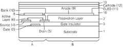
도 1A 및 도 1B는 본 발명의 실시예들에 따른 유기전자발광 디스플레이의 개략적 단면도이다. 이러한 도 1A, 1B는 유기 전자발광 디스플레이에서 하나의 서브 픽셀의 개략적 단면도로서 화소 회로부의 구성요소인 스위칭 트랜지스터와 스토리지 커패시터 및 구동 트랜지스터 중 스위칭 트랜지스터 및 스토리지 커패시터는 생략되고 드라이빙 트랜지스터 및 이에 의해 구동되는 OLED의 적층 구조만을 보인다.1A and 1B are schematic cross-sectional views of an organic electroluminescent display according to embodiments of the present invention. 1A and 1B are schematic cross-sectional views of one sub-pixel in an organic electroluminescent display. Among the switching transistors, the storage capacitors, and the driving transistors, which are components of the pixel circuit unit, the switching transistors and the storage capacitors are omitted, and the driving transistors and the OLEDs driven therefrom Only the laminated structure is shown.
도 1A에서는 "A" 영역은 화소 회로부가 배치되는 영역이며 "B" 영역은 화소 회로부에 의해 구동되는 OLED가 배치되는 영역이다. "A" 영역을 살펴보면, 기판(1) 위에 게이트(2)가 형성되고 이 위에 게이트 절연층(3)이 형성된다. 게이트 절연층(3)은 "A" 영역뿐 아니라 "B" 영역도 덮는다. 게이트 절연층(3) 위에는 게이트(2)를 중심으로 그 양측에 배치되는 소스(4)와 드레인(5)이 형성된다. 소스(4)와 드레인(5) 위에는 그 양단이 소스(4)와 드레인(5)에 걸쳐지는 유기 또는 무기 반도체 물질로 된 활성층(Active Layer, 6)이 형성된다. 상기 활성층(6) 위에는 평탄화층으로서의 패시베이션층(7)이 형성되며, 이 패시베이션층(8)은 "B" 영역에까지 확장된다. 상기 패시베이션층(7) 위에는 ITO 또는 IZO 등의 투명 도전성 물질로 된 보호층(8)과 애노드 전극(9)이 형성된다. 상기 보호층(8)은 화소 회로부가 형성되는 "A" 영역에 위치하며, 애노드 전극(9)은 OLED 가 배치되는 영역인 "B" 영역에 위치한다.In FIG. 1A, an area "A" is an area in which a pixel circuit part is arranged and an area "B" is an area in which an OLED driven by the pixel circuit part is arranged. Referring to the area "A", the
상기 보호층(8)과 애노드 전극(9) 위에는 뱅크(10)가 형성된다. 여기에서 애노드 전극(9) 부분은 윈도우(10a)를 통해 노출된다. 뱅크(10)와 뱅크(10)에 덮이지 않은 애노드 전극(9) 위에는 정공수송층 및 발광층을 포함하는 유기발광층(11)이 형성되고, 그 위에 전면적으로 금속 등의 반사성 도전물질로 된 캐소오드 전극(12) 및 실링층(13)이 형성된다.A
위에서 설명된 본 발명에 따른 유기 전자발광 디스플레이는 애노드 전극(9)을 형성하는 단계에서 동시에 제작된 화소 회로부의 보호층(8)을 가진다는 점에 특징이 있다. 보호층(8)은 애노드를 위한 플라즈마 표면 처리 및 유기 액상물질에 의한 유기발광층(11) 형성 단계 전에 트랜지스터를 포함하는 화소 회로부를 덮음으로써 플라즈마 및 유기 액상물질에 의한 화소 회로부, 특히 화소 회로부의 트랜지스터의 손상을 방지한다. 이러한 트랜지스터의 손상방지의 효과는 유기 패시베이션막을 사용한 경우에 두드러지게 나타나며, 유기 반도체의 경우에 특히 필요하다.The organic electroluminescent display according to the invention described above is characterized in that it has a
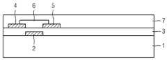
도 1B는 뱅크가 없는 구조로서 뱅크를 제외한 나머지 구조는 동일하다. 도 1B를 참조하면, "A" 영역을 살펴보면, 기판(1) 위에 게이트(2), 게이트 절연층(3), 소스/드레인(4, 5), 활성층(Active Layer, 6), 패시베이션층(7), 보호층(8)이 순차적으로 형성된다. 게이트 절연층(3)과 패시베이션층(8)은 역시 "A" 영역과 "B" 영역에 공히 형성된다. "B" 영역을 살펴보면, 기판(1) 위에 게이트 절연층(3), 패시베이션층(7) 애노드 전극(9)이 형성된다. 상기 애노드 전극(9)은 상기 보호층(8)과 동일물질로 동시에 제조된다. 상기 보호층(8)은 전기적으로 고립되어 있고 단순히 화소 회로부를 보호하는 기능만을 가진다.1B is a structure without a bank, and the rest of the structure is the same except for the bank. Referring to FIG. 1B, referring to region “A”, a
전술한 실시예는 p-채널 TFT를 이용하는 유기 전자발광 디스플레이이며, 본 발명의 다른 실시예에 따른 n-채널 TFT 가 적용될 수 있다. 이 경우 OLED의 애노드가 구동 트랜지스터의 소스에 연결되며 케소오드는 접지된다.The above embodiment is an organic electroluminescent display using a p-channel TFT, and an n-channel TFT according to another embodiment of the present invention can be applied. In this case, the anode of the OLED is connected to the source of the driving transistor and the cathode is grounded.
위의 실시예들에서 설명된 구동 회로부는 기본적으로 유기 반도체 재료를 이용하는 것으로 설명되었으나 본 발명의 다른 실시예에 따르면 실리콘이나 ZnO 등의 무기 반도체 재료가 적용될 수 있으며 이러한 재료의 선택에 의해 다른 요소들의 재료도 적절히 변경되어야 할 것이며, 이러한 재료의 선택은 공지된 기술에 의해 용이하며 따라서 본 발명의 기술적 범위를 제한하지 않는다.The driving circuit portion described in the above embodiments has been described as basically using an organic semiconductor material, but according to another embodiment of the present invention, an inorganic semiconductor material such as silicon or ZnO may be applied, and by the selection of such materials, The materials will also have to be changed as appropriate, the selection of such materials is easy by known techniques and therefore does not limit the technical scope of the present invention.
한편, 유기반도체재료의 경우 p-형 반도체 재료로 펜타센(pentacene)이 사용될 수 있으며 소스와 드레인 전극은 Au 또는 Cr/Au로 형성될 수 있다. 그리고 n-형 유기 반도체 재료로는 F16CuPc 또는 NTCDA, DHF-6T을 이용할 수 있다. 게이트 절연층 및 패시베이션층은 잘 알려진 절연성 유기 또는 무기재료를 이용한다. 유기재료에는 PVP, PVA 무기 재료에는 SiO2, Si2N3, Al2O3, SiRiO3 등이 있다. 그리고 뱅크 재료로는 PVA(Polyvinylacetate) PA(Photo Acryl), PI(Polyimide) 또는 블랙 포토 레지스트드의 카본계열 유기재료가 있다. 기판은 PES, PET, PC 등의 플라스틱이나 유리가 적용될 수 있다.Meanwhile, in the case of the organic semiconductor material, pentacene may be used as the p-type semiconductor material, and the source and drain electrodes may be formed of Au or Cr / Au. F16CuPc, NTCDA, or DHF-6T may be used as the n-type organic semiconductor material. The gate insulating layer and the passivation layer use well-known insulating organic or inorganic materials. Organic materials include PVP, and PVA inorganic materials include SiO2, Si2N3, Al2O3, SiRiO3, and the like. The bank material may be a carbon-based organic material such as polyvinylacetate (PVA) photo acryl (PA), polyimide (PI), or black photoresist. The substrate may be plastic or glass such as PES, PET, or PC.
이하에서, 도 2A - 2J를 참조하면서 도 1A에 도시된 유기 전자발광 디스플레이의 제조방법을 설명하며 이를 통해서 도 1B에 도시된 유기전자발광디스플레이의 제조방법은 용이하게 이해할 수 있을 것이다.Hereinafter, a method of manufacturing the organic electroluminescent display shown in FIG. 1A will be described with reference to FIGS. 2A-2J, and a method of manufacturing the organic electroluminescent display shown in FIG. 1B will be readily understood.
도 2A 에 도시된 바와 같이, 투명한 기판(1) 위에 게이트(2)를 형성한다.As shown in FIG. 2A, a
도 2B에 도시된 바와 같이, 상기 게이트(2)가 형성된 기판(1) 전체 위에 게이트 절연층(3)을 형성한다. 전술한 바와 같이 PVP, PVA 등의 유기재료 또는 SiO2, Si2N3, Al2O3, SiRiO3 등의 무기재료를 이용한다.As shown in FIG. 2B, a
도 2C에 도시된 바와 같이, 게이트(2)의 상방 양측에 소스(4)와 드레인(5)을 형성한다. 이때의 재료로 Au 및 Cr을 이용하여 Au 단일층 또는 Cr/Au 2중 층 구조의 소스(4)와 드레인(5)을 형성한다.As shown in FIG. 2C, the
도 2D에 도시된 바와 같이, 펜타센 등의 유기 반도체 물질을 증착한 후 이를 패터닝 하여 상기 소스(4)와 드레인(5)의 사이에 활성층(6)을 형성한다.As shown in FIG. 2D, an organic semiconductor material such as pentacene is deposited and then patterned to form an
도 2E에 도시된 바와 같이, 상기 구성 요소들이 형성되는 기판(1) 위에 평탄화층으로서 전술한 바와 같은 절연성 유기 또는 무기재료로 패시베이션층(7)을 형성한다.As shown in Fig. 2E, the
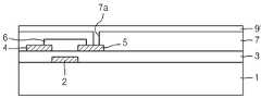
도 2F에 도시된 바와 같이, 상기 패시베이션층(7)에 비아홀(7a)을 형성한 후, 이 위에 ITO 등의 투명 도전성 물질(9')을 증착한다.As shown in FIG. 2F, a via
도 2G에 도시된 바와 같이 상기 투명 도전성 물질(9')을 패터닝 하여 전술한 바와 같은 보호층(8) 및 애노드 전극(9)을 형성한다.As shown in Fig. 2G, the transparent conductive material 9 'is patterned to form the
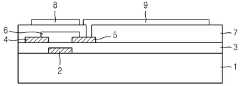
도 2H에 도시된 바와 같이 상기 기판 위에 애노드 전극(9)의 표면이 노출되는 윈도우(10a)를 갖는 뱅크(10)를 PVA, PA, PI 또는 블랙 포토 레지스트 등을 이용하여 형성한다.As shown in FIG. 2H, a
도 2I에 도시된 바와 같이 플라즈마를 이용해 애노드 전극(9)의 표면 에너지 조절을 위한 표면처리를 행한다. 이 과정에서 뱅크(10)의 매몰되어 있는 보호층(8)은 상기 플라즈마로부터 그 하부의 화소 회로부를 보호한다.As shown in FIG. 2I, surface treatment for surface energy control of the
도 2J에 도시된 바와 같이 상기 뱅크 위에 알려진 바와 같은 구조로서 유기물질을 이용해 정공수송층 및 발광층을 포함하는 유기발광층(11)을 순차적으로 형성하고 그 위에 금속 등의 반사성 도전물질로 된 캐소오드 전극(12) 및 실링층(13)을 형성하여 목적하는 유기 전자발광디스플레이를 얻는다. 역시 이 과정에서 상기 보호층(8)은 유기물질의 침투를 차단하여 그 하부의 화소 회로부를 보호한다.As shown in FIG. 2J, an organic
상기와 같이 본 발명의 디스플레이는 스위칭 트랜지스터, 드라이빙 트랜지스터가 포함된 화소 회로부가 그 위의 투명 전극 물질에 의한 보호층에 의해 보호되는 구조를 가진다.As described above, the display of the present invention has a structure in which a pixel circuit portion including a switching transistor and a driving transistor is protected by a protective layer made of a transparent electrode material thereon.
이러한 본 발명에 따르면, 투명 애노드 전극에 대해 행해지는 플라즈마 표면처리시 플라즈마로부터 구동 회로부가 상기 보호층에 의해 보호하고, 또한 유기발광층 형성시 유기 물질에 포함된 유기용재의 침투를 차단하여 역시 구동 회로부가 보호된다.According to the present invention, the driving circuit portion is protected by the protective layer from the plasma during the plasma surface treatment performed on the transparent anode electrode, and also the driving circuit portion by blocking the penetration of the organic material contained in the organic material when forming the organic light emitting layer Is protected.
이러한 본 발명은 특히 유기 박막 트랜지스터를 이용하는 배면 발광형(BOTTOM EMISSION) 유기 전자발광 디스플레이 및 그 제조방법에 적용되기에 적합하다.The present invention is particularly suitable for application to a bottom emission organic electroluminescent display using an organic thin film transistor and a method of manufacturing the same.
이러한 본원 발명의 이해를 돕기 위하여 몇몇의 모범적인 실시예가 설명되고 첨부된 도면에 도시되었으나, 이러한 실시예들은 단지 넓은 발명을 예시하고 이를 제한하지 않는다는 점이 이해되어야 할 것이며, 그리고 본 발명은 도시되고 설명된 구조와 배열에 국한되지 않는다는 점이 이해되어야 할 것이며, 이는 다양한 다른 수정이 당 분야에서 통상의 지식을 가진 자에게 일어날 수 있기 때문이다.While some exemplary embodiments have been described and illustrated in the accompanying drawings in order to facilitate understanding of the present invention, it should be understood that these embodiments merely illustrate the broad invention and do not limit it, and the invention is illustrated and described. It is to be understood that the invention is not limited to structured arrangements and arrangements, as various other modifications may occur to those skilled in the art.
Claims (12)
Translated fromKoreanPriority Applications (2)
| Application Number | Priority Date | Filing Date | Title |
|---|---|---|---|
| KR1020060013068AKR100754395B1 (en) | 2006-02-10 | 2006-02-10 | Organic electroluminescent display and manufacturing method thereof |
| US11/555,493US7425730B2 (en) | 2006-02-10 | 2006-11-01 | Organic electro-luminescent display and fabrication method thereof |
Applications Claiming Priority (1)
| Application Number | Priority Date | Filing Date | Title |
|---|---|---|---|
| KR1020060013068AKR100754395B1 (en) | 2006-02-10 | 2006-02-10 | Organic electroluminescent display and manufacturing method thereof |
Publications (2)
| Publication Number | Publication Date |
|---|---|
| KR20070081250A KR20070081250A (en) | 2007-08-16 |
| KR100754395B1true KR100754395B1 (en) | 2007-08-31 |
Family
ID=38367458
Family Applications (1)
| Application Number | Title | Priority Date | Filing Date |
|---|---|---|---|
| KR1020060013068AActiveKR100754395B1 (en) | 2006-02-10 | 2006-02-10 | Organic electroluminescent display and manufacturing method thereof |
Country Status (2)
| Country | Link |
|---|---|
| US (1) | US7425730B2 (en) |
| KR (1) | KR100754395B1 (en) |
Families Citing this family (11)
| Publication number | Priority date | Publication date | Assignee | Title |
|---|---|---|---|---|
| JP2007103584A (en)* | 2005-10-03 | 2007-04-19 | Ricoh Co Ltd | Transistor element, display device, and manufacturing method thereof |
| KR20080013300A (en)* | 2006-08-08 | 2008-02-13 | 삼성전자주식회사 | Thin film transistor array panel and manufacturing method thereof |
| GB2461670B (en)* | 2007-04-25 | 2012-05-16 | Merck Patent Gmbh | Process for preparing an electronic device |
| KR100963104B1 (en) | 2008-07-08 | 2010-06-14 | 삼성모바일디스플레이주식회사 | Thin film transistor, its manufacturing method, and flat panel display device comprising thin film transistor |
| KR101810699B1 (en)* | 2009-06-30 | 2018-01-25 | 가부시키가이샤 한도오따이 에네루기 켄큐쇼 | Method for manufacturing semiconductor device |
| JP5969745B2 (en)* | 2010-09-10 | 2016-08-17 | 株式会社半導体エネルギー研究所 | Semiconductor device |
| TWI467301B (en)* | 2012-10-24 | 2015-01-01 | Au Optronics Corp | Display panel |
| KR102279015B1 (en) | 2014-06-30 | 2021-07-19 | 엘지디스플레이 주식회사 | Self healing polymer and flexible display comprising the same |
| WO2018186867A1 (en)* | 2017-04-06 | 2018-10-11 | Hewlett-Packard Development Company, L.P. | Rigid carriers for plastic layers of devices |
| CN111092099A (en)* | 2018-10-23 | 2020-05-01 | 宸鸿光电科技股份有限公司 | Organic light emitting diode display device |
| CN110854287A (en)* | 2019-10-23 | 2020-02-28 | 武汉华星光电半导体显示技术有限公司 | OLED display panel, preparation method thereof and display device |
Citations (2)
| Publication number | Priority date | Publication date | Assignee | Title |
|---|---|---|---|---|
| US6538390B2 (en)* | 2000-09-06 | 2003-03-25 | Sharp Kabushiki Kaisha | Organic LED display device of active matrix drive type and fabrication method therefor |
| US6836070B2 (en)* | 2001-10-17 | 2004-12-28 | Chi Mei Optoelectronics Corporation | Organic electro-luminescent display and method of sealing the same |
Family Cites Families (5)
| Publication number | Priority date | Publication date | Assignee | Title |
|---|---|---|---|---|
| US6825496B2 (en)* | 2001-01-17 | 2004-11-30 | Semiconductor Energy Laboratory Co., Ltd. | Light emitting device |
| TW588471B (en)* | 2003-04-24 | 2004-05-21 | Delta Optoelectronics Inc | Active matrix organic light emitting diode and fabricating method thereof |
| JP2005277065A (en)* | 2004-03-24 | 2005-10-06 | Pioneer Electronic Corp | Circuit element and manufacturing method thereof |
| US7396852B2 (en)* | 2005-11-16 | 2008-07-08 | Xerox Corporation | Compound having indolocarbazole moiety and divalent linkage |
| US7425723B2 (en)* | 2005-12-21 | 2008-09-16 | Xerox Corporation | Organic thin-film transistors |
- 2006
- 2006-02-10KRKR1020060013068Apatent/KR100754395B1/enactiveActive
- 2006-11-01USUS11/555,493patent/US7425730B2/enactiveActive
Patent Citations (2)
| Publication number | Priority date | Publication date | Assignee | Title |
|---|---|---|---|---|
| US6538390B2 (en)* | 2000-09-06 | 2003-03-25 | Sharp Kabushiki Kaisha | Organic LED display device of active matrix drive type and fabrication method therefor |
| US6836070B2 (en)* | 2001-10-17 | 2004-12-28 | Chi Mei Optoelectronics Corporation | Organic electro-luminescent display and method of sealing the same |
Also Published As
| Publication number | Publication date |
|---|---|
| US20070187680A1 (en) | 2007-08-16 |
| US7425730B2 (en) | 2008-09-16 |
| KR20070081250A (en) | 2007-08-16 |
Similar Documents
| Publication | Publication Date | Title |
|---|---|---|
| KR100754395B1 (en) | Organic electroluminescent display and manufacturing method thereof | |
| KR100427883B1 (en) | Self light emitting display panel and meth od for manufacturing the same | |
| US9595691B2 (en) | Organic light emitting diode device | |
| US8044582B2 (en) | Organic display apparatus comprising moisture propagation preventing means | |
| EP2019432B1 (en) | Organic light emitting display and method of manufacturing the same | |
| KR102045036B1 (en) | Organic Light Emitting Diode Display Having High Aperture Ratio And Method For Manufacturing The Same | |
| US9741782B2 (en) | Active matrix organic light-emitting display and display apparatus | |
| KR101908514B1 (en) | Organic light emitting display device and method for fabricating the same | |
| KR102062912B1 (en) | Organic Light Emitting Diode Display And Method For Manufacturing The Same | |
| KR101979369B1 (en) | Organic light emitting diode display | |
| CN105810716A (en) | Flexible display device and preparation method | |
| KR20150060195A (en) | Organic light emitting diode device and method of fabricating the same | |
| KR20160093173A (en) | Display device and manufacturing method thereof | |
| JP2007227129A (en) | Organic EL device and method for manufacturing organic EL device | |
| KR100745760B1 (en) | Organic electroluminescent display and manufacturing method thereof | |
| KR101084248B1 (en) | Organic light emitting display | |
| JP2001100655A (en) | El display device | |
| KR20150033345A (en) | Organic Light Emitting Diode Display And Method For Manufacturing The Same | |
| KR20150017193A (en) | Organic light emitting diode display | |
| KR100685841B1 (en) | Organic electroluminescent display and manufacturing method thereof | |
| KR102053440B1 (en) | Organic Light Emitting Diode Display Having High Aperture Ratio And Method For Manufacturing The Same | |
| KR20140057839A (en) | Organic light emitting display device and method for fabricating the same | |
| KR102037487B1 (en) | Method for fabricating Organic Electroluminescence Device and the Organic Electroluminescence Device fabricated by the method | |
| US20060214564A1 (en) | Organic electroluminescent display and method for fabricating the same | |
| KR102593450B1 (en) | Organic Light Emitting Display Device |
Legal Events
| Date | Code | Title | Description |
|---|---|---|---|
| A201 | Request for examination | ||
| PA0109 | Patent application | Patent event code:PA01091R01D Comment text:Patent Application Patent event date:20060210 | |
| PA0201 | Request for examination | ||
| E902 | Notification of reason for refusal | ||
| PE0902 | Notice of grounds for rejection | Comment text:Notification of reason for refusal Patent event date:20070130 Patent event code:PE09021S01D | |
| E701 | Decision to grant or registration of patent right | ||
| PE0701 | Decision of registration | Patent event code:PE07011S01D Comment text:Decision to Grant Registration Patent event date:20070725 | |
| PG1501 | Laying open of application | ||
| GRNT | Written decision to grant | ||
| PR0701 | Registration of establishment | Comment text:Registration of Establishment Patent event date:20070827 Patent event code:PR07011E01D | |
| PR1002 | Payment of registration fee | Payment date:20070828 End annual number:3 Start annual number:1 | |
| PG1601 | Publication of registration | ||
| PR1001 | Payment of annual fee | Payment date:20100812 Start annual number:4 End annual number:4 | |
| PR1001 | Payment of annual fee | Payment date:20110816 Start annual number:5 End annual number:5 | |
| FPAY | Annual fee payment | Payment date:20120814 Year of fee payment:6 | |
| PR1001 | Payment of annual fee | Payment date:20120814 Start annual number:6 End annual number:6 | |
| FPAY | Annual fee payment | Payment date:20130731 Year of fee payment:7 | |
| PR1001 | Payment of annual fee | Payment date:20130731 Start annual number:7 End annual number:7 | |
| FPAY | Annual fee payment | Payment date:20160801 Year of fee payment:10 | |
| PR1001 | Payment of annual fee | Payment date:20160801 Start annual number:10 End annual number:10 | |
| FPAY | Annual fee payment | Payment date:20180802 Year of fee payment:12 | |
| PR1001 | Payment of annual fee | Payment date:20180802 Start annual number:12 End annual number:12 | |
| PR1001 | Payment of annual fee | Payment date:20200803 Start annual number:14 End annual number:14 | |
| PR1001 | Payment of annual fee | Payment date:20210802 Start annual number:15 End annual number:15 | |
| PR1001 | Payment of annual fee | Payment date:20230801 Start annual number:17 End annual number:17 | |
| PR1001 | Payment of annual fee | Payment date:20240723 Start annual number:18 End annual number:18 |