KR100754065B1 - Method of manufacturing printed circuit board with embedded resistor - Google Patents
Method of manufacturing printed circuit board with embedded resistorDownload PDFInfo
- Publication number
- KR100754065B1 KR100754065B1KR1020030077949AKR20030077949AKR100754065B1KR 100754065 B1KR100754065 B1KR 100754065B1KR 1020030077949 AKR1020030077949 AKR 1020030077949AKR 20030077949 AKR20030077949 AKR 20030077949AKR 100754065 B1KR100754065 B1KR 100754065B1
- Authority
- KR
- South Korea
- Prior art keywords
- copper foil
- resistance
- paste
- resistor
- printed circuit
- Prior art date
- Legal status (The legal status is an assumption and is not a legal conclusion. Google has not performed a legal analysis and makes no representation as to the accuracy of the status listed.)
- Expired - Fee Related
Links
Images


Classifications
- H—ELECTRICITY
- H05—ELECTRIC TECHNIQUES NOT OTHERWISE PROVIDED FOR
- H05K—PRINTED CIRCUITS; CASINGS OR CONSTRUCTIONAL DETAILS OF ELECTRIC APPARATUS; MANUFACTURE OF ASSEMBLAGES OF ELECTRICAL COMPONENTS
- H05K3/00—Apparatus or processes for manufacturing printed circuits
- H05K3/30—Assembling printed circuits with electric components, e.g. with resistor
- H—ELECTRICITY
- H05—ELECTRIC TECHNIQUES NOT OTHERWISE PROVIDED FOR
- H05K—PRINTED CIRCUITS; CASINGS OR CONSTRUCTIONAL DETAILS OF ELECTRIC APPARATUS; MANUFACTURE OF ASSEMBLAGES OF ELECTRICAL COMPONENTS
- H05K1/00—Printed circuits
- H05K1/16—Printed circuits incorporating printed electric components, e.g. printed resistor, capacitor, inductor
- H05K1/167—Printed circuits incorporating printed electric components, e.g. printed resistor, capacitor, inductor incorporating printed resistors
- B—PERFORMING OPERATIONS; TRANSPORTING
- B23—MACHINE TOOLS; METAL-WORKING NOT OTHERWISE PROVIDED FOR
- B23K—SOLDERING OR UNSOLDERING; WELDING; CLADDING OR PLATING BY SOLDERING OR WELDING; CUTTING BY APPLYING HEAT LOCALLY, e.g. FLAME CUTTING; WORKING BY LASER BEAM
- B23K26/00—Working by laser beam, e.g. welding, cutting or boring
- B23K26/351—Working by laser beam, e.g. welding, cutting or boring for trimming or tuning of electrical components
- B—PERFORMING OPERATIONS; TRANSPORTING
- B23—MACHINE TOOLS; METAL-WORKING NOT OTHERWISE PROVIDED FOR
- B23K—SOLDERING OR UNSOLDERING; WELDING; CLADDING OR PLATING BY SOLDERING OR WELDING; CUTTING BY APPLYING HEAT LOCALLY, e.g. FLAME CUTTING; WORKING BY LASER BEAM
- B23K2101/00—Articles made by soldering, welding or cutting
- B23K2101/36—Electric or electronic devices
- B23K2101/42—Printed circuits
- H—ELECTRICITY
- H05—ELECTRIC TECHNIQUES NOT OTHERWISE PROVIDED FOR
- H05K—PRINTED CIRCUITS; CASINGS OR CONSTRUCTIONAL DETAILS OF ELECTRIC APPARATUS; MANUFACTURE OF ASSEMBLAGES OF ELECTRICAL COMPONENTS
- H05K1/00—Printed circuits
- H05K1/02—Details
- H05K1/09—Use of materials for the conductive, e.g. metallic pattern
- H05K1/092—Dispersed materials, e.g. conductive pastes or inks
- H05K1/095—Dispersed materials, e.g. conductive pastes or inks for polymer thick films, i.e. having a permanent organic polymeric binder
- H—ELECTRICITY
- H05—ELECTRIC TECHNIQUES NOT OTHERWISE PROVIDED FOR
- H05K—PRINTED CIRCUITS; CASINGS OR CONSTRUCTIONAL DETAILS OF ELECTRIC APPARATUS; MANUFACTURE OF ASSEMBLAGES OF ELECTRICAL COMPONENTS
- H05K2201/00—Indexing scheme relating to printed circuits covered by H05K1/00
- H05K2201/03—Conductive materials
- H05K2201/0332—Structure of the conductor
- H05K2201/0335—Layered conductors or foils
- H05K2201/0347—Overplating, e.g. for reinforcing conductors or bumps; Plating over filled vias
- H—ELECTRICITY
- H05—ELECTRIC TECHNIQUES NOT OTHERWISE PROVIDED FOR
- H05K—PRINTED CIRCUITS; CASINGS OR CONSTRUCTIONAL DETAILS OF ELECTRIC APPARATUS; MANUFACTURE OF ASSEMBLAGES OF ELECTRICAL COMPONENTS
- H05K2203/00—Indexing scheme relating to apparatus or processes for manufacturing printed circuits covered by H05K3/00
- H05K2203/14—Related to the order of processing steps
- H05K2203/1461—Applying or finishing the circuit pattern after another process, e.g. after filling of vias with conductive paste, after making printed resistors
- H—ELECTRICITY
- H05—ELECTRIC TECHNIQUES NOT OTHERWISE PROVIDED FOR
- H05K—PRINTED CIRCUITS; CASINGS OR CONSTRUCTIONAL DETAILS OF ELECTRIC APPARATUS; MANUFACTURE OF ASSEMBLAGES OF ELECTRICAL COMPONENTS
- H05K3/00—Apparatus or processes for manufacturing printed circuits
- H05K3/02—Apparatus or processes for manufacturing printed circuits in which the conductive material is applied to the surface of the insulating support and is thereafter removed from such areas of the surface which are not intended for current conducting or shielding
- H05K3/06—Apparatus or processes for manufacturing printed circuits in which the conductive material is applied to the surface of the insulating support and is thereafter removed from such areas of the surface which are not intended for current conducting or shielding the conductive material being removed chemically or electrolytically, e.g. by photo-etch process
- H05K3/061—Etching masks
- H05K3/064—Photoresists
- H—ELECTRICITY
- H05—ELECTRIC TECHNIQUES NOT OTHERWISE PROVIDED FOR
- H05K—PRINTED CIRCUITS; CASINGS OR CONSTRUCTIONAL DETAILS OF ELECTRIC APPARATUS; MANUFACTURE OF ASSEMBLAGES OF ELECTRICAL COMPONENTS
- H05K3/00—Apparatus or processes for manufacturing printed circuits
- H05K3/10—Apparatus or processes for manufacturing printed circuits in which conductive material is applied to the insulating support in such a manner as to form the desired conductive pattern
- H05K3/108—Apparatus or processes for manufacturing printed circuits in which conductive material is applied to the insulating support in such a manner as to form the desired conductive pattern by semi-additive methods; masks therefor
- Y—GENERAL TAGGING OF NEW TECHNOLOGICAL DEVELOPMENTS; GENERAL TAGGING OF CROSS-SECTIONAL TECHNOLOGIES SPANNING OVER SEVERAL SECTIONS OF THE IPC; TECHNICAL SUBJECTS COVERED BY FORMER USPC CROSS-REFERENCE ART COLLECTIONS [XRACs] AND DIGESTS
- Y10—TECHNICAL SUBJECTS COVERED BY FORMER USPC
- Y10T—TECHNICAL SUBJECTS COVERED BY FORMER US CLASSIFICATION
- Y10T29/00—Metal working
- Y10T29/49—Method of mechanical manufacture
- Y10T29/49002—Electrical device making
- Y10T29/49082—Resistor making
- Y10T29/49087—Resistor making with envelope or housing
- Y10T29/49098—Applying terminal
- Y—GENERAL TAGGING OF NEW TECHNOLOGICAL DEVELOPMENTS; GENERAL TAGGING OF CROSS-SECTIONAL TECHNOLOGIES SPANNING OVER SEVERAL SECTIONS OF THE IPC; TECHNICAL SUBJECTS COVERED BY FORMER USPC CROSS-REFERENCE ART COLLECTIONS [XRACs] AND DIGESTS
- Y10—TECHNICAL SUBJECTS COVERED BY FORMER USPC
- Y10T—TECHNICAL SUBJECTS COVERED BY FORMER US CLASSIFICATION
- Y10T29/00—Metal working
- Y10T29/49—Method of mechanical manufacture
- Y10T29/49002—Electrical device making
- Y10T29/49082—Resistor making
- Y10T29/49101—Applying terminal
- Y—GENERAL TAGGING OF NEW TECHNOLOGICAL DEVELOPMENTS; GENERAL TAGGING OF CROSS-SECTIONAL TECHNOLOGIES SPANNING OVER SEVERAL SECTIONS OF THE IPC; TECHNICAL SUBJECTS COVERED BY FORMER USPC CROSS-REFERENCE ART COLLECTIONS [XRACs] AND DIGESTS
- Y10—TECHNICAL SUBJECTS COVERED BY FORMER USPC
- Y10T—TECHNICAL SUBJECTS COVERED BY FORMER US CLASSIFICATION
- Y10T29/00—Metal working
- Y10T29/49—Method of mechanical manufacture
- Y10T29/49002—Electrical device making
- Y10T29/49117—Conductor or circuit manufacturing
- Y10T29/49124—On flat or curved insulated base, e.g., printed circuit, etc.
- Y10T29/49126—Assembling bases
- Y—GENERAL TAGGING OF NEW TECHNOLOGICAL DEVELOPMENTS; GENERAL TAGGING OF CROSS-SECTIONAL TECHNOLOGIES SPANNING OVER SEVERAL SECTIONS OF THE IPC; TECHNICAL SUBJECTS COVERED BY FORMER USPC CROSS-REFERENCE ART COLLECTIONS [XRACs] AND DIGESTS
- Y10—TECHNICAL SUBJECTS COVERED BY FORMER USPC
- Y10T—TECHNICAL SUBJECTS COVERED BY FORMER US CLASSIFICATION
- Y10T29/00—Metal working
- Y10T29/49—Method of mechanical manufacture
- Y10T29/49002—Electrical device making
- Y10T29/49117—Conductor or circuit manufacturing
- Y10T29/49124—On flat or curved insulated base, e.g., printed circuit, etc.
- Y10T29/4913—Assembling to base an electrical component, e.g., capacitor, etc.
- Y—GENERAL TAGGING OF NEW TECHNOLOGICAL DEVELOPMENTS; GENERAL TAGGING OF CROSS-SECTIONAL TECHNOLOGIES SPANNING OVER SEVERAL SECTIONS OF THE IPC; TECHNICAL SUBJECTS COVERED BY FORMER USPC CROSS-REFERENCE ART COLLECTIONS [XRACs] AND DIGESTS
- Y10—TECHNICAL SUBJECTS COVERED BY FORMER USPC
- Y10T—TECHNICAL SUBJECTS COVERED BY FORMER US CLASSIFICATION
- Y10T29/00—Metal working
- Y10T29/49—Method of mechanical manufacture
- Y10T29/49002—Electrical device making
- Y10T29/49117—Conductor or circuit manufacturing
- Y10T29/49124—On flat or curved insulated base, e.g., printed circuit, etc.
- Y10T29/49147—Assembling terminal to base
- Y10T29/49151—Assembling terminal to base by deforming or shaping
- Y—GENERAL TAGGING OF NEW TECHNOLOGICAL DEVELOPMENTS; GENERAL TAGGING OF CROSS-SECTIONAL TECHNOLOGIES SPANNING OVER SEVERAL SECTIONS OF THE IPC; TECHNICAL SUBJECTS COVERED BY FORMER USPC CROSS-REFERENCE ART COLLECTIONS [XRACs] AND DIGESTS
- Y10—TECHNICAL SUBJECTS COVERED BY FORMER USPC
- Y10T—TECHNICAL SUBJECTS COVERED BY FORMER US CLASSIFICATION
- Y10T29/00—Metal working
- Y10T29/49—Method of mechanical manufacture
- Y10T29/49002—Electrical device making
- Y10T29/49117—Conductor or circuit manufacturing
- Y10T29/49124—On flat or curved insulated base, e.g., printed circuit, etc.
- Y10T29/49155—Manufacturing circuit on or in base
- Y10T29/49156—Manufacturing circuit on or in base with selective destruction of conductive paths
Landscapes
- Engineering & Computer Science (AREA)
- Microelectronics & Electronic Packaging (AREA)
- Physics & Mathematics (AREA)
- Optics & Photonics (AREA)
- Plasma & Fusion (AREA)
- Mechanical Engineering (AREA)
- Manufacturing & Machinery (AREA)
- Parts Printed On Printed Circuit Boards (AREA)
- Apparatuses And Processes For Manufacturing Resistors (AREA)
Abstract
Translated fromKoreanDescription
Translated fromKorean도1a 내지 도1e는 종래의 방법에 따른 매립된 저항을 갖는 인쇄회로기판을 제조 방법을 순차적으로 나타낸다.1A to 1E sequentially illustrate a method of manufacturing a printed circuit board having a buried resistor according to a conventional method.
도2a 내지 도2d는 본 발명에 따른 매립된 저항을 갖는 인쇄회로기판의 제조 방법을 나타낸다.2A to 2D show a method of manufacturing a printed circuit board having a buried resistor according to the present invention.
도3a 내지 도3d는 본 발명에 따른 매립된 저항을 갖는 인쇄회로기판 제조 방법에서 동박의 상태를 순차적으로 나타낸 사시도이다.3A to 3D are perspective views sequentially showing the state of copper foil in a method of manufacturing a printed circuit board having a buried resistor according to the present invention.
도4는 본 발명의 일 실시예에 따른 인쇄회로기판 제조 방법 중 접촉 저항을 줄이기 위한 금속을 추가적으로 도금한 인쇄회로기판의 단면을 나타낸다.4 is a cross-sectional view of a printed circuit board additionally plated with a metal for reducing contact resistance in a method of manufacturing a printed circuit board according to an embodiment of the present invention.
도5는 도4에 도시된 인쇄회로기판의 동박 부분에 대한 사시도이다.5 is a perspective view of a copper foil portion of the printed circuit board shown in FIG.
도6a 내지 도6e는 본 발명의 또다른 실시예에 따른 매립된 저항을 갖는 인쇄회로기판의 제조 방법을 순차적으로 나타낸다.6A through 6E sequentially illustrate a method of manufacturing a printed circuit board having a buried resistor according to another embodiment of the present invention.
도7a 내지 도7e는 도6a 내지 도6e에 도시된 본 발명의 매립된 저항을 갖는 인쇄회로기판 제조 방법에서 동박의 상태를 순차적으로 나타낸 사시도이다.7A to 7E are perspective views sequentially showing the state of copper foil in the method of manufacturing a printed circuit board having a buried resistor of the present invention shown in FIGS. 6A to 6E.
도8a 내지 도8h는 본 발명의 또다른 실시예에 따른 매립된 저항을 갖는 인쇄회로기판의 제조 방법을 순차적으로 나타낸다.8A to 8H sequentially illustrate a method of manufacturing a printed circuit board having a buried resistor according to another embodiment of the present invention.
도9a는 도8b의 도금 레지스트 패턴이 형성된 동박층의 사시도이고, 도9b는 도8h의 저항 페이스트가 연마 가공된 동박의 사시도이다.Fig. 9A is a perspective view of the copper foil layer on which the plating resist pattern of Fig. 8B is formed, and Fig. 9B is a perspective view of the copper foil on which the resist paste of Fig. 8H is polished.
※ 도면의 주요 부분에 대한 설명※ Description of the main parts of the drawings
21,61,81 : 동박적층판21,61,81: Copper Clad Laminated Plate
22,62,82 : 동박층22,62,82: Copper foil layer
23,63,83 : 보강기재23,63,83: Reinforcement materials
24, 64 : 저항이 매립될 부분24, 64: part where the resistance is buried
26,66,88 : 저항 페이스트26,66,88: Resistance Paste
28 : 접지 단자용 은 도금층28: silver plating layer for ground terminal
67 : 금속층67 metal layer
본 발명은 매립된 저항을 갖는 인쇄회로기판의 제조 방법에 관한 것이다.The present invention relates to a method of manufacturing a printed circuit board having a buried resistor.
보다 구체적으로, 본 발명은 저항 페이스트를 정확한 모양과 부피를 갖는 저항체로 형성하여 저항값을 균일하게 맞춤으로써 레이저 트리밍 작업을 하지 않거나 혹은 최소화 하여, 제조시간을 단축시키고 인쇄장비의 위치정밀도에 큰 영향을 받지 않고 빠르게 작업조건 설정이 가능하여 생산성이 향상되며, 스크린 프린팅에 의한 저항 형성 등 종래 방식에 비해 균일한 저항 페이스트의 도포 두께의 확보함으로써 저항값 편차를 개선시키고 쉽게 저항을 형성할 수 있는 매립된 저항을 갖는 인쇄회로기판 제조 방법에 관한 것이다.More specifically, the present invention forms a resistor paste with a resistor having an accurate shape and volume to uniformly adjust the resistance value so that laser trimming is not performed or minimized, thereby shortening the manufacturing time and greatly affecting the positional accuracy of the printing equipment. The productivity can be improved by setting the working conditions quickly without receiving the resistance, and by securing the uniform coating thickness of the resistance paste compared to the conventional method such as the resistance formation by screen printing, the resistance value variation can be improved and the landfill can be easily formed. It relates to a printed circuit board manufacturing method having a predetermined resistance.
인쇄회로기판은 전자회로의 부품을 장착하는 기판으로서 판상에서 대부분의 배선이 노광 및 에칭에 의하여 형성되고, 그 위에 특정한 회로설계에 따라 부품이 실장되고 결선된다. 일반적으로, 전자기기에는 다수의 능동부품 및 수동부품들이 회로기판의 표면에 실장되어 있으며, 수동부품 중에서 특히 저항은 별개의 칩 저항(discrete chip resistor)의 형태로 능동부품들 간의 신호 전달을 원활히 하기 위하여 많은 수가 표면에 실장되어 있다. 그러나 별개의 칩 저항으로는 전자부품의 경박단소화 추세에 부응하는데 한계가 있었고, 공간활용 측면에서도 문제가 있었다.A printed circuit board is a board on which components of an electronic circuit are mounted, and most wirings are formed by exposure and etching on a plate, and components are mounted and connected thereon according to a specific circuit design. In general, in electronic devices, a large number of active and passive components are mounted on the surface of a circuit board. Among the passive components, resistors are particularly used to facilitate signal transmission between active components in the form of discrete chip resistors. Many are mounted on the surface. However, there was a limit to meet the trend of light and short of electronic components with separate chip resistors, and there was a problem in terms of space utilization.
상기 문제점을 해결하기 위하여, 새로운 재료 또는 물질 및 공정을 이용하여 전술한 별개의 칩 저항을 대체하는 방법으로서 인쇄회로기판 자체에 저항을 매립시키는 방법이 제시되었다.In order to solve the above problem, a method of embedding a resistor in the printed circuit board itself has been proposed as a method of replacing the above-described separate chip resistance using a new material or material and process.
이러한 매립형의 저항을 갖는 인쇄회로기판은 기판 자체의 내부 또는 외부에 수동소자인 저항이 매립되어 있는 형태로서 기판자체의 크기에 관계없으며, 수동소자가 기판의 부분으로 통합되어 있는 형태이다. 즉, 수동소자가 기판의 일부분으로 포함되어 있기 때문에 별개의 칩 저항을 기판의 표면에 실장하거나 연결할 필요가 없는 특징을 갖는다. 따라서, 상기 별개의 칩 저항이 차지하고 있던 공간을 다른 부품용으로 이용하여 고집적의 실장면적을 확보할 수 있으며, 인쇄회로기판의 크기를 더욱 감소시켜 전자기기의 소형화 추세에도 부응할 수 있고, 솔더 조인트(solder joint)의 제거, 열 또는 기계적 충격 및 진동에 영향을 감소시켜 신 뢰성을 요하는 기기에 적합한 장점을 갖는다.A printed circuit board having a buried resistor has a form in which a resistor, which is a passive element, is embedded inside or outside the substrate itself, regardless of the size of the substrate itself, and a passive element is integrated into a portion of the substrate. That is, since the passive element is included as part of the substrate, there is no need to mount or connect a separate chip resistor to the surface of the substrate. Therefore, by using the space occupied by the separate chip resistors for other components, a high integration area can be secured, and the size of the printed circuit board can be further reduced to meet the trend of miniaturization of electronic devices, and solder joints. Elimination of solder joints, reducing the impact on thermal or mechanical shock and vibration, has the advantage of being suitable for equipment requiring reliability.
이처럼, 매립형의 저항을 형성하기 위하여 다양한 방법이 개발되어 왔으며, 현재 상용화된 방법은 다음과 같다.As such, various methods have been developed to form a buried resistor, and currently commercialized methods are as follows.
첫째, 세라믹 저항 페이스트를 도포하고 소성하여 구현하는 세라믹 후막 형태의 저항(thick film typed resistor)를 형성하는 기술이 있다. 상기 기술은 통상 세라믹 저항 페이스트를 기판의 표면에 도포하고, 약 850∼900℃의 고온에서 소성한 다음, 스크린 프린팅에 의하여 상기 저항을 보호하기 위한 유리층을 도포한 후에 재소성하는 과정으로 이루어진다. 이러한 세라믹 저항의 구현기술은 미국특허번호 제5,510,594호에 구체적으로 개시되어 있다. 상기 특허에서는 알루미나와 같은 전기적으로 절연된 물질로 제조된 기판(substrate) 상에 은을 함유하는 전도성 물질로 제조된 전극을 형성한 후에 서어밋(cermet)과 같은 저항물질로 제조된 후막 저항을 상기 전극과 전기적으로 연결되도록 형성하고, 레이저 트리밍(laser trimming)을 통하여 원하는 저항값을 구현하고, 그리고 상기 전극 및 저항을 보호하기 위한 절연성의 보호 필름을 형성하고 있다. 그러나, 상기 기술은 세라믹 기판에 적용되는 것으로서 에폭시-글라스, 폴리이미드 등의 수지계 기판에 직접적으로 적용하기는 곤란하다.First, there is a technology of forming a thick film typed resistor, which is formed by applying and firing a ceramic resistor paste. The technique typically involves applying a ceramic resistor paste to the surface of a substrate, firing at a high temperature of about 850 to 900 ° C., and then applying a glass layer to protect the resistance by screen printing, followed by refiring. A technique for implementing such a ceramic resistor is specifically disclosed in US Patent No. 5,510,594. The patent describes a thick film resistor made of a resistive material such as cermet after forming an electrode made of a conductive material containing silver on a substrate made of an electrically insulated material such as alumina. It is formed to be electrically connected to the electrode, to implement the desired resistance value through laser trimming (laser trimming), and to form an insulating protective film for protecting the electrode and the resistance. However, the above technique is applied to ceramic substrates, and it is difficult to directly apply to resin-based substrates such as epoxy-glass and polyimide.
둘째, 인쇄회로기판 내부에 저항특성을 갖는 별도의 금속층 또는 금속막을 형성하여 인쇄회로기판의 표면에 실장되던 저항을 대체하는 박막 형태의 저항(thin film typed resistor)를 구현하는 기술이 있다. 이와 관련하여, Ohmega-Ply?(Ohmega Technologies, Inc.의 상품명)라는 박막의 저항물질을 사용하여 매립된 저항을 갖는 인쇄회로기판의 제조방법이 이미 상용화된 바 있다.Second, there is a technology for forming a thin film typed resistor to replace the resistor mounted on the surface of the printed circuit board by forming a separate metal layer or a metal film having a resistance characteristic inside the printed circuit board. In this regard, Ohmega-Ply? (Method of Ohmega Technologies, Inc.) A method of manufacturing a printed circuit board having a buried resistor using a thin film of resist material has already been commercialized.
예를 들면, 미국특허번호 제4,892,776호에서 개시하고 있는 지지층(support layer); 니켈-포스포로스(Nickel-Phosporous) 조성을 갖고, 상기 지지층과 결합된 적어도 하나의 저항층(resistant layer); 및 상기 저항층에 결합된 전도층(conductive layer)으로 이루어지는 저항물질을 사용하고, 사진석판술(photolithographic process)을 통하여 매립된 저항을 갖는 인쇄회로기판을 제조할 수 있다. 상기 방법에서는 저항체가 인쇄회로기판의 내부에 형성되어 절연체에 의해 저항체가 보호되므로 외부 환경에 의한 영향을 방지하기 위하여 별도의 공법을 필요로 하지 않는다.For example, the support layer disclosed in US Patent No. 4,892,776; At least one resistive layer having a nickel-phosphorous composition and bonded to the support layer; And a resistive material comprising a conductive layer bonded to the resistive layer, and a printed circuit board having a resistive buried through a photolithographic process can be manufactured. In the above method, since the resistor is formed inside the printed circuit board and the resistor is protected by the insulator, a separate method is not required to prevent the influence of the external environment.
셋째, 기판 상에 고분자계 저항 페이스트를 도포하고 열건조(경화)시키는 고분자 후막 형태의 저항을 구현하는 기술이 있다. 상기 기술은 기판의 내층에 도포하는 내장형 및 최외층에 페이스트를 도포하는 외장형으로 구분된다.Third, there is a technique for implementing a polymer thick film-type resistance to apply the polymer-based resistance paste on the substrate and heat-drying (curing). The technique is divided into a built-in type applied to the inner layer of the substrate and an outer type applied paste to the outermost layer.
이러한 내장형 기술과 관련한 선행기술은 예를 들면, EP 0 569 801 A1 및 일본 특개평 6-61651호에 개시되어 있다. 즉, 상기 기술에 따르면 저항은 양측면 상에 도체선로가 구비된 인쇄회로기판의 내층에 프린팅에 의하여 후막상으로 형성되고 표면실장소자(SMD)가 외층 상에 실장되며, 상기 인쇄회로기판이 유전물질로 이루어진 중간층 상에서 상기 내층이 상호 마주보면서 프레스되어 있다. 상기 내장형 기술은 기판 내부에 저항이 형성되어 외부 환경에 의한 영향을 억제하기 위한 별도의 저항 보호층을 필요로 하지 않는다. 그러나, 저항의 저항값의 예측성(predictability) 및 허용한계(tolerance limitation)의 조절에 있어서는 불리하다.Prior art with regard to such embedded technologies is disclosed, for example, in EP 0 569 801 A1 and Japanese Patent Laid-Open No. 6-61651. That is, according to the above technology, the resistance is formed in a thick film by printing on the inner layer of the printed circuit board having the conductor lines on both sides, and the surface mount device is mounted on the outer layer, and the printed circuit board is a dielectric material. The inner layers are pressed while facing each other on an intermediate layer made of. The embedded technology does not require a separate resistive protection layer to form a resistance inside the substrate to suppress the influence of the external environment. However, it is disadvantageous in adjusting the predictability and tolerance limitation of the resistance value of the resistance.
한편, 외장형 기술의 경우, 저항특성을 갖는 고분자를 사용하여 스크린 프린팅을 통하여 기판산상에 도포한 후에 솔더 마스크(또는 솔더 레지스트)를 인쇄하여 고분자 저항을 보호하는 방법이다.On the other hand, in the case of the external technology, a polymer having resistance characteristics is applied to the substrate acid through screen printing and then a solder mask (or solder resist) is printed to protect the polymer resistance.
도1a 내지 도1e는 종래의 기술에 따른 외장형의 매립된 저항을 갖는 인쇄회로기판을 제조하는 공정을 순차적으로 도시하는 도면이다.1A to 1E are diagrams sequentially showing a process of manufacturing a printed circuit board having an external embedded resistor according to the prior art.
먼저 도 1a와 같이 기판(1)에 도전층(구리 박막)(2)을 형성한 다음, 상기 도전층이 형성된 기판(1)의 최외층 상에 포토레지스트 필름 또는 드라이 필름 층(3, 3')을 형성시키고, 노광(exposure), 현상(development), 구리 에칭(copper etching) 과정을 통하여 도전층(2)에 특정 패턴의 구리 단자를 형성시킨다(제1 단계).First, a conductive layer (copper thin film) 2 is formed on the
제1 단계에서 에칭 레지스트로 사용된 드라이 필름(3, 3')을 스트리핑하여 도 도 1b와 같이 일정한 간격에 의하여 상호 격치되는 구리 단자(copper termination; 2, 2')를 형성한다(제2 단계).Stripping the
그 다음, 카본계 저항 페이스트(5)를 상기 구리 단자(2, 2') 사이에 스퀴즈 블레이드(4) 등을 사용하여 도 1c와 같이 스크린 프린팅한다(제3 단계).Then, the carbon-based resist
상기 과정에서, 저항 페이스트를 도포한 후에는 약 150∼250℃에서 가열 건조하여 열경화시키고, 도 1d와 같이 형성된 후막 저항(6)는 상기 각각의 구리 단자(2, 2')와 전기적으로 연결된다(제4 단계).In the above process, after the application of the resistance paste, heat-cured by heat drying at about 150 ~ 250 ℃, the
그리고 나서, 선택적으로 레이저 트리밍에 의해 도포된 저항 페이스트를 절삭하여 원하는 저항값을 얻는다. 이와 관련하여, 미국특허번호 제5,510,594호는 레이저 트리밍을 통하여 원하는 저항값을 구현하는 방법을 제시하고 있다. 그러나, 상기 특허의 경우, 전술한 바와 같이 기판의 재질이 세라믹으로 구성되어 있기 때문에 레이저 트리밍 과정이 비교적 용이하고 원하는 저항값을 구현할 수 있는 반면, 보다 넓은 면적 및 플라스틱 재질을 갖는 인쇄회로기판의 경우에는 레이저 트리밍의 정확성 면에서 문제가 있고, 레이저 열에 의하여 저항값이 변동되고 트리밍 가공비용이 상당히 고가이기 때문에 실제 인쇄회로기판에 적용되기는 곤란하였다.Thereafter, the applied resistance paste is optionally cut by laser trimming to obtain a desired resistance value. In this regard, US Patent No. 5,510,594 proposes a method of implementing a desired resistance value through laser trimming. However, in the case of the patent, since the substrate material is made of ceramic as described above, the laser trimming process is relatively easy and the desired resistance value can be realized, whereas in the case of a printed circuit board having a larger area and a plastic material There is a problem in the accuracy of laser trimming, it is difficult to apply to the actual printed circuit board because the resistance value is changed by the laser heat and the trimming processing cost is very expensive.
그 다음, 도 1e와 같이 기판에 형성된 후막 저항(6)의 상부에 솔더 마스크 잉크(solder mask ink 또는 PSR ink; 7)를 사용하여 솔더 마스크 층(7)을 형성시킴으로써 외부환경에 의한 손상, 예컨대 물리적, 화학적 손상, 습기 또는 온도에 의한 저항특성의 변화를 방지하도록 한다(제5 단계).Then, by forming a
그러나, 상기 언급된 외장형 기술의 경우, 제2 단계와 제3 단계 사이의 공정지연으로 인하여 노출된 구리 단자(2,2')가 외부환경에 의하여 쉽게 산화되고, 이처럼 산화된 단자 상에 다시 액상의 저항 페이스트가 도포되고 건조되면 구리 산화가 촉진된다. 따라서, 저항와 단자의 계면에서의 접착력이 저하되어 저항값이 상승하는 문제점이 발생한다. 상기와 같은 흡습에 의한 저항상승을 고려하여 미리 저항의 저항값을 작게 조절하는 방안도 시도되고 있으나 양산에는 부적합하다.However, in the case of the above-mentioned external technology, the exposed
또한, 세라믹 인쇄회로기판의 경우, 일반적으로 기판의 크기가 10×10㎝ 이 상을 초과하는 예는 거의 없으나 수지계 인쇄회로기판은 통상적으로 50×60㎝ 정도의 판넬(panel) 크기이므로 저항 페이스트를 기판 상에 도포하면 동일 판넬 내에서 위치별로 저항 페이스트의 두께가 불균일하게 인쇄되는 경향이 있으며, 이러한 두께의 불균일성은 저항값의 불균일 현상을 유발하여 제품의 신뢰성을 저하시키는 요인이 되고 있다.In addition, in the case of ceramic printed circuit boards, in general, there are few examples in which the size of the substrate is larger than 10 × 10 cm or more, but resin-based printed circuit boards generally have a panel size of about 50 × 60 cm. When applied onto a substrate, the thickness of the resist paste tends to be unevenly printed for each position in the same panel, and the non-uniformity of the thickness causes a non-uniformity of the resistance value, thereby degrading the reliability of the product.
보다 구체적으로, 저항의 저항값은 하기 수학식 1에 의하여 계산될 수 있다:More specifically, the resistance value of the resistance can be calculated by the following equation (1):
R(저항값) = R(비저항) x (레지스터 길이)/ (레지스터 폭 x 레지스터 두께)R (Resistance) = R (Resistance) x (Register Length) / (Register Width x Resistor Thickness)
상기 수학식에서 알 수 있듯이, 저항의 두께가 증가하면 저항값은 감소하게되는데 실제 인쇄공정에 있어서 판넬 상에 일정한 두께로 인쇄하는 것은 인쇄제판, 인쇄기와 같은 설비 자체의 인쇄편차(tolerance)로 인하여 균일한 저항값을 구현하기 곤란하다.As can be seen from the above equation, as the thickness of the resistance increases, the resistance value decreases. Printing in a certain thickness on the panel in the actual printing process is uniform due to the tolerance of the equipment itself, such as a printing plate and a printing press. It is difficult to realize a resistance value.
또한, 이러한 종래의 스크린 인쇄에 의한 매립 저항 형성 방법에서는 스크린 인쇄의 해상도에 한계가 있어 정확한 저항의 폭을 구현하기 힘들고, 인쇄의 특성상 접점이 되는 패드의 크기를 크게 해야하며, 저항의 중심부분이 단자의 높이보다 낮아지는 정도를 균일하게 하기 어려워 정밀한 저항값을 얻기 어렵기 때문에 레이저 트리밍 공정이 필수적이었다.In addition, in the conventional method of forming a buried resistor by screen printing, the resolution of screen printing is limited, so it is difficult to realize a precise width of resistance, and the size of the pad to be a contact is large due to the characteristics of printing. The laser trimming process was essential because it is difficult to uniformize the degree of falling below the height of the terminal and it is difficult to obtain a precise resistance value.
또한, 종래의 스크린 인쇄에 의한 매립 저항 형성 방법에서는, 위치에 따라 균일하게 저항을 형성하기 어려우며, 단자 위에 저항이 돌출되어 있어 공정 진행 중에 파손 우려 및 자동화에 어려움이 있었다.In addition, in the conventional method of forming a buried resistor by screen printing, it is difficult to form a resistance uniformly according to the position, and a resistance protrudes on the terminal, and thus there is a fear of damage and difficulty in automation during the process.
전술한 종래기술의 문제점을 고려하여, 외부환경에 의한 저항값의 변화를 최소화할 수 있고, 이와 함께 원하는 저항값을 정확히 구현할 수 있는, 새로운 후막 저항이 매립된 인쇄회로기판에 대한 개발이 절실히 요청되고 있다.In view of the above-described problems of the prior art, there is an urgent need for the development of a printed circuit board with a new thick film resistor, which can minimize a change in resistance due to an external environment and accurately implement a desired resistance value. It is becoming.
본 발명은 종래 방법에 비해 저항 페이스트이 인쇄 공정의 정밀도에 크게 좌우되지 않고, 종래의 스크린 프린팅에 사용되는 고가의 스크린 망사 없이도 작업 효율을 매우 향상시킬 수 있는 매립된 저항을 갖는 인쇄회로기판 제조 방법을 제공하는 것을 목적으로 한다.The present invention provides a method of manufacturing a printed circuit board having a buried resistor that can significantly improve the working efficiency without the expensive screen mesh used for conventional screen printing, since the resist paste is not significantly dependent on the precision of the printing process compared with the conventional method. It aims to provide.
또한, 본 발명은 인쇄회로기판에 도포되는 저항의 두께가 인쇄장비의 위치에 따라 좌우되지 않고, 동박층의 두께에 따라 좌우되므로 도포두께를 보다 균일하게 형성할 수 있는 매립된 저항을 갖는 인쇄회로기판 제조 방법을 제공하는 것을 목적으로 한다.In addition, the present invention is a printed circuit having a buried resistor that can be formed more uniformly because the thickness of the resistor applied to the printed circuit board is not dependent on the position of the printing equipment, but depends on the thickness of the copper foil layer. It is an object to provide a substrate manufacturing method.
또한, 본 발명은 형성된 저항이 주위의 동박 표면과 일치하므로, 적층을 하는 경우 압력에 의한 변형이 없어 적층 후 저항값 변화량을 일정하게 유지할 수 있는 매립된 저항을 갖는 인쇄회로기판 제조 방법을 제공하는 것을 목적으로 한다.In addition, the present invention provides a printed circuit board manufacturing method having a buried resistance that can maintain a constant resistance change after lamination because there is no deformation caused by pressure when the resistance is formed to match the surface of the surrounding copper foil. For the purpose of
또한, 본 발명은 요구되는 저항의 정밀도에 따라 레이저 트리밍 공정 없이도 원하는 저항값을 형성할 수 있는 매립된 저항을 갖는 인쇄회로기판 제조 방법을 제공하는 것을 목적으로 한다.In addition, an object of the present invention is to provide a method for manufacturing a printed circuit board having a buried resistor capable of forming a desired resistance value without a laser trimming process according to the required precision of the resistance.
또한, 본 발명은 회로의 폭보다 넓은 접점 패드를 필요로 하지 않고 다른 소 자와 전기적으로 연결할 수 있는 매립된 저항을 갖는 인쇄회로기판 제조 방법을 제공하는 것을 목적으로 한다.In addition, an object of the present invention is to provide a method for manufacturing a printed circuit board having a buried resistor that can be electrically connected to other elements without requiring a contact pad wider than the width of the circuit.
또한, 본 발명은 저항을 인쇄회로기판의 내부에 삽입하여 단위면적당 부품밀도를 증가시킴으로써, 고집적 전자기기에 사용될 수 있는 매립된 저항을 갖는 인쇄회로기판 제조 방법을 제공하는 것을 목적으로 한다.In addition, an object of the present invention is to provide a method of manufacturing a printed circuit board having a buried resistance that can be used for highly integrated electronic devices by inserting a resistor into the printed circuit board to increase the component density per unit area.
또한, 본 발명은 진공 인쇄를 통해 저항 페이스트에 보이드(void) 형성을 억제하여 더욱 정밀한 저항값을 얻을 수 있는 매립된 저항을 갖는 인쇄회로기판 제조 방법을 제공하는 것을 목적으로 한다.In addition, an object of the present invention is to provide a method for manufacturing a printed circuit board having a buried resistor that can suppress the formation of voids in the resistor paste through vacuum printing to obtain a more accurate resistance value.
또한, 본 발명은 인쇄회로기판 내에서 저항의 위치에 따른 편차가 거의 없어 제조 공정의 신뢰성이 확보할 수 있는 매립된 저항을 갖는 인쇄회로기판 제조 방법을 제공하는 것을 목적으로 한다.In addition, an object of the present invention is to provide a method for manufacturing a printed circuit board having a buried resistance that can be secured in the reliability of the manufacturing process because there is almost no variation in the position of the resistance in the printed circuit board.
또한, 본 발명은 인쇄회로기판의 외곽 뿐만 아니라 내부 어느 층에도 매립 저항을 형성할 수 있고, 내부에 저항을 형성하는 경우에는 프레스 공정 등의 경우에도 저항 파손을 최소화할 수 있는 매립된 저항을 갖는 인쇄회로기판 제조 방법을 제공하는 것을 목적으로 한다.In addition, the present invention can form a buried resistor in any layer as well as the outside of the printed circuit board, and in the case of forming a resistor therein has a buried resistor that can minimize resistance breakdown even in the case of a press process or the like An object of the present invention is to provide a method for manufacturing a printed circuit board.
본 발명에 따른 매립된 저항을 갖는 인쇄회로기판 제조 방법은, 동박적층판의 동박 중 저항이 삽입될 부분에 해당하는 동박을 제거하는 단계; 상기 동박이 제거된 부분에 저항 페이스트를 충진하는 단계; 및 상기 저항 페이스트가 충진된 동박적층판에 회로 패턴을 형성하는 단계를 포함하는 것을 특징으로 한다.According to the present invention, there is provided a method of manufacturing a printed circuit board having a buried resistor, the method including: removing a copper foil corresponding to a portion of a copper foil laminated sheet into which a resistance is to be inserted; Filling the resist paste into the portion where the copper foil is removed; And forming a circuit pattern on the copper foil laminated plate filled with the resistor paste.
보다 바람직하게는, 본 발명에 따른 매립된 저항을 갖는 인쇄회로기판 제조 방법에서, 상기 저항 페이스트를 충진하는 단계는, 상기 충진된 저항 페이스트를 건조하는 단계; 및 상기 충진된 저항 페이스트를 주변의 동박층의 두께와 동일하도록 연마 가공하는 단계를 더 포함하는 것을 특징으로 한다.More preferably, in the method of manufacturing a printed circuit board having a buried resistor according to the present invention, the filling of the resistor paste may include: drying the filled resistor paste; And grinding the filled resistance paste to be equal to the thickness of the surrounding copper foil layer.
보다 바람직하게는, 본 발명에 따른 매립된 저항을 갖는 인쇄회로기판 제조 방법에서, 상기 저항 페이스트를 충진하는 단계는 진공 인쇄기에 의해 수행되는 것을 특징으로 한다.More preferably, in the method of manufacturing a printed circuit board having a buried resistor according to the present invention, the filling of the resistor paste is performed by a vacuum printer.
보다 바람직하게는, 본 발명에 따른 매립된 저항을 갖는 인쇄회로기판 제조 방법은, 상기 저항 페이스트를 충진하는 단계 전에 상기 저항이 삽입될 부분의 동박 내벽에 은, 금, 니켈 또는 백금층을 형성하는 단계를 더 포함하는 것을 특징으로 한다.More preferably, the method of manufacturing a printed circuit board having a buried resistor according to the present invention comprises forming a silver, gold, nickel or platinum layer on the inner wall of the copper foil of the portion where the resistor is to be inserted before the filling of the resistor paste. It further comprises a step.
보다 바람직하게는, 본 발명에 따른 매립된 저항을 갖는 인쇄회로기판 제조 방법은, 상기 회로 패턴을 형성하는 단계 전에 매립된 저항의 접점 부위에 은, 금, 니켈 또는 백금을 도금하는 단계를 더 포함하는 것을 특징으로 한다.More preferably, the method of manufacturing a printed circuit board having a buried resistor according to the present invention further includes plating silver, gold, nickel or platinum on the contact portion of the buried resistor before forming the circuit pattern. Characterized in that.
본 발명의 또다른 실시예에 따른 매립된 저항을 갖는 인쇄회로기판 제조 방법은, 동박적층판의 동박 중 저항이 삽입될 부분에 해당하는 동박을 제거하는 단계; 상기 동박이 제거된 부분에 저항 페이스트를 충진하는 단계; 상기 저항 페이스트가 충진된 동박적층판 전면에 금속층을 도금하는 단계; 및 상기 동박적층판에 회로 패턴을 형성하는 단계를 포함하는 것을 특징으로 한다.According to still another aspect of the present invention, there is provided a method of manufacturing a printed circuit board having a buried resistor, the method including: removing a copper foil corresponding to a portion of a copper foil laminated sheet into which a resistance is to be inserted; Filling the resist paste into the portion where the copper foil is removed; Plating a metal layer on an entire surface of the copper-clad laminate filled with the resistance paste; And forming a circuit pattern on the copper clad laminate.
보다 바람직하게는, 본 발명의 또다른 실시예에 따른 매립된 저항을 갖는 인 쇄회로기판 제조 방법에서, 상기 저항 페이스트를 충진하는 단계는, 상기 충진된 저항 페이스트를 건조하는 단계; 및 상기 충진된 저항 페이스트를 다른 동박층의 두께와 동일하도록 연마 가공하는 단계를 더 포함하는 것을 특징으로 한다.More preferably, in the method of manufacturing a printed circuit board having a buried resistor according to another embodiment of the present invention, the filling of the resistor paste may include: drying the filled resistor paste; And grinding the filled resistance paste to be equal to the thickness of the other copper foil layer.
보다 바람직하게는, 본 발명의 또다른 실시예에 따른 매립된 저항을 갖는 인쇄회로기판 제조 방법에서, 상기 저항 페이스트를 충진하는 단계는 진공 인쇄기에 의해 수행되는 것을 특징으로 한다.More preferably, in the method of manufacturing a printed circuit board having a buried resistor according to another embodiment of the present invention, the filling of the resistor paste is performed by a vacuum printer.
보다 바람직하게는, 본 발명의 또다른 실시예에 따른 매립된 저항을 갖는 인쇄회로기판 제조 방법은, 상기 저항 페이스트를 충진하는 단계 전에 상기 저항이 삽입될 부분의 동박 내벽에 은, 금, 니켈 또는 백금을 도금하는 단계를 더 포함하는 것을 특징으로 한다.More preferably, a method of manufacturing a printed circuit board having a buried resistor according to another embodiment of the present invention may include silver, gold, nickel or silver on the inner wall of the copper foil of the portion where the resistor is to be inserted before the filling of the resistor paste. It is characterized in that it further comprises the step of plating platinum.
보다 바람직하게는, 본 발명의 또다른 실시예에 따른 매립된 저항을 갖는 인쇄회로기판 제조 방법은, 상기 저항 페이스트 충진 후 상기 매립된 저항 페이스트의 접점 부위에 전기전도도가 좋은 물질을 형성하는 단계를 더 포함하는 것을 특징으로 한다.More preferably, according to another embodiment of the present invention, a method of manufacturing a printed circuit board having a buried resistor may include forming a material having good electrical conductivity at a contact portion of the buried resistor paste after filling the resistor paste. It further comprises.
본 발명의 또다른 실시예에 따른 매립된 저항을 갖는 인쇄회로기판 제조 방법은, 동박적층판의 표면에 저항이 삽입될 부분에 해당하는 도금 레지스트 패턴을 형성하는 단계; 상기 동박적층판을 도금하는 단계; 상기 저항이 삽입될 부분의 동박층을 에칭하기 위한 에칭 레지스트 패턴을 형성하는 단계; 상기 도금 레지스트 패턴을 제거하는 단계; 상기 동박적층판을 에칭하는 단계; 상기 저항이 삽입될 부분에 저항 페이스트를 충진하는 단계; 및 상기 동박적층판에 회로 패턴을 형성하는 단계를 포함하는 것을 특징으로 한다.In another aspect of the present invention, there is provided a method of manufacturing a printed circuit board having a buried resistor, the method including: forming a plating resist pattern corresponding to a portion where a resistance is to be inserted into a surface of a copper clad laminate; Plating the copper clad laminate; Forming an etching resist pattern for etching the copper foil layer of the portion where the resistance is to be inserted; Removing the plating resist pattern; Etching the copper-clad laminate; Filling a resistor paste in a portion into which the resistor is to be inserted; And forming a circuit pattern on the copper clad laminate.
보다 바람직하게는, 본 발명의 또다른 실시예에 따른 매립된 저항을 갖는 인쇄회로기판 제조 방법에서, 상기 저항 페이스트를 충진하는 단계는, 상기 충진된 저항 페이스트를 건조하는 단계; 및 상기 충진된 저항 페이스트를 다른 동박층의 두께와 동일하도록 연마 가공하는 단계를 더 포함하는 것을 특징으로 한다.More preferably, in the method of manufacturing a printed circuit board having a buried resistor according to another embodiment of the present invention, the filling of the resistor paste may include: drying the filled resistor paste; And grinding the filled resistance paste to be equal to the thickness of the other copper foil layer.
보다 바람직하게는, 본 발명의 또다른 실시예에 따른 매립된 저항을 갖는 인쇄회로기판 제조 방법에서, 상기 저항 페이스트를 충진하는 단계는 진공 인쇄기에 의해 수행되는 것을 특징으로 한다.More preferably, in the method of manufacturing a printed circuit board having a buried resistor according to another embodiment of the present invention, the filling of the resistor paste is performed by a vacuum printer.
보다 바람직하게는, 본 발명의 또다른 실시예에 따른 매립된 저항을 갖는 인쇄회로기판 제조 방법은, 상기 저항 페이스트를 충진하는 단계 전에 상기 저항이 삽입될 부분의 동박 내벽에 은, 금, 니켈 또는 백금을 도금하는 단계를 더 포함하는 것을 특징으로 한다.More preferably, a method of manufacturing a printed circuit board having a buried resistor according to another embodiment of the present invention may include silver, gold, nickel or silver on the inner wall of the copper foil of the portion where the resistor is to be inserted before the filling of the resistor paste. It is characterized in that it further comprises the step of plating platinum.
보다 바람직하게는, 본 발명의 또다른 실시예에 따른 매립된 저항을 갖는 인쇄회로기판 제조 방법은, 상기 회로 패턴을 형성하는 단계 전에 매립된 저항의 접점 부위에 은, 금, 니켈 또는 백금을 도금하는 단계를 더 포함하는 것을 특징으로 한다.More preferably, the method of manufacturing a printed circuit board having a buried resistor according to another embodiment of the present invention, plating silver, gold, nickel or platinum on the contact portion of the buried resistor before the step of forming the circuit pattern Characterized in that it further comprises the step.
본 발명의 또다른 실시예에 따른 매립된 저항을 갖는 인쇄회로기판 제조 방법은, 상기 저항페이스트가 충진된 동박적층판 전면을 금속물질로 도금하는 단계를 더 포함하는 것을 특징으로 한다.The method of manufacturing a printed circuit board having a buried resistor according to another embodiment of the present invention may further include plating the entire surface of the copper-clad laminate filled with the resistance paste with a metal material.
이하, 도면을 참조하여 본 발명을 보다 상세히 설명한다.Hereinafter, the present invention will be described in more detail with reference to the drawings.
도2a 내지 2d는 본 발명의 일 실시예에 따른 매립된 저항을 갖는 인쇄회로기판의 제조 방법을 나타낸다.2A to 2D illustrate a method of manufacturing a printed circuit board having a buried resistor according to an embodiment of the present invention.
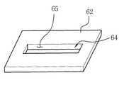
도2a는 베이스 기판으로 사용되는 동박 적층판(21)의 단면을 나타낸다. 동박적층판(21)은 보강 기재(23)에 동박(22)을 입힌 얇은 적층판이다. 동박적층판(21)으로는 여러 가지 종류를 사용할 수 있으나, 비용면에서 볼 때 유리 섬유에 에폭시 수지를 침투시킨 보강 기재에 동박을 입힌 수지계 인쇄회로기판인 소위 FR-4 동박 적층판을 사용하는 것이 유리하다.2A shows a cross section of a copper foil laminated
그리고 나서, 동박적층판(21)의 동박(22) 전면에 에칭 레지스트를 도포하고, 저항 페이스트가 충진될 부분(24)이 인쇄된 마스크 필름을 대고, 노광 및 현상에 의해 에칭 레지스트 패턴을 형성한다. 그리고 나서, 에칭에 의해 저항 페이스트가 충진될 부분의 동박을 제거한다.Then, an etching resist is applied to the entire surface of the
도2b는 이와 같이 에칭에 의해 저항 페이스트가 충진될 부분(24)이 제거된 인쇄회로기판의 단면도이다. 에칭 레지스트로는 드라이 필름을 사용하는 것이 바람직하다.FIG. 2B is a cross-sectional view of the printed circuit board in which the
도3a는 이와 같이 저항 페이스트가 충진될 부분의 동박이 제거된 상태의 사시도를 나타낸다. 도3a에는 설명을 위해 동박(22)만이 도시되어 있으며 보강기재(23)는 미도시되어 있다.Fig. 3A shows a perspective view of a state in which the copper foil of the portion to be filled with the resist paste is removed. Only
실시예에 따라서는, 저항 페이스트의 접촉 저항에 따른 저항 편차를 낮추기 위해 동박이 제거된 동박의 내벽(25)에 은, 금, 백금 또는 니켈 등 전기 전도성이 좋은 금속을 도금할 수도 있다.In some embodiments, a metal having good electrical conductivity such as silver, gold, platinum or nickel may be plated on the
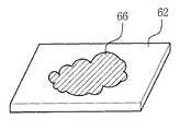
도2c에서, 인쇄기를 사용하여 동박이 제거된 부분(24)에 동박과 거의 같은 높이가 되도록 저항 페이스트(26)를 충진한다. 이때, 상기 저항 페이스트로는 여러 종류가 사용될 수 있지만, 카본 블랙과 같은 입자에 고분자를 메트릭스로 하는 카본계 저항 페이스트를 사용하는 것이 바람직하다.In Fig. 2C, the resist
충진 방법은 통상적인 스크린 인쇄기를 이용하는 것도 가능하지만, 저항 편차를 줄이고, 저항 페이스트에 보이드(void) 형성을 억제하기 위해서는 진공 인쇄기를 사용하는 것이 바람직하다.Although the filling method can also use a conventional screen printing machine, it is preferable to use a vacuum printing machine in order to reduce the resistance variation and to suppress the formation of voids in the resistance paste.
진공 인쇄기는 인쇄회로기판제작에서 일반적으로 사용되는 스크린 인쇄기와 유사한 것이나, 일반 스크린 인쇄기는 대기에 노출된 상태에서 미세홀 속에 잉크를 밀어 넣는 것으로 이 경우에는 충진한 잉크의 내부에 기포가 다량 포함되어 있는데, 이러한 현상을 막기 위해서 인쇄 작업이 되는 부위를 진공으로 만들어 진공상태에서 인쇄작업이 이루어 지도록 한 장비가 진공 인쇄기이다. 진공 인쇄기는 일반 스크린 인쇄기로 인쇄하는 것에 비하여 충진된 잉크내부에 기포가 없으며, 한쪽이 막혀진 홀 속에 잉크를 충진하는 경우에도 용이하게 충진할 수 있는 장점이 있다.Vacuum printing machines are similar to the screen printing machines commonly used in printed circuit board fabrication, but ordinary screen printing machines push ink into the microholes when exposed to the atmosphere. In this case, a large amount of bubbles are contained inside the filled ink. In order to prevent such a phenomenon, a vacuum printing machine is a device which makes a printing work in a vacuum state by making a printing part into a vacuum. Compared to printing with a general screen printing machine, the vacuum printing machine has no bubble inside the filled ink, and has an advantage that it can be easily filled even when the ink is filled in a hole in which one side is blocked.
그리고 나서, 충진된 저항 페이스트(26)를 약 150∼250℃에서 가열 건조하여 열경화시킨다. 이와 같이 저항 페이스트(26)가 충진된 상태의 동박층(22)의 사시도가 도3b에 도시되어 있다.Then, the filled
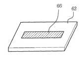
도2d에서, 연마 가공에 의해 동박에 비해 위로 돌출된 부분의 저항 페이스트를 제거하여 저항 페이스트(26)가 다른 동박과 정확히 같은 높이가 되도록 한다. 이와 같이 연마 가공된 상태의 동박층(22)의 사시도가 도3c에 도시되어 있다.In Fig. 2D, the resist paste of the portion protruding upward relative to the copper foil is removed by polishing so that the resist
그리고 나서, 에칭에 의해 동박적층판(21)의 동박(22)에 에칭 레지스트 패턴을 형성한 다음, 에칭에 의해 회로 패턴을 형성하면 매립된 저항을 갖는 인쇄회로기판이 완성된다. 도3d에는 이와 같이 회로 패턴이 형성된 저항(26)이 매립된 동박(22)의 사시도를 나타낸다.Then, an etching resist pattern is formed on the
상기 회로 패턴을 형성하는 공정에는 비아홀 형성 및 도금, 적층 등의 통상적인 인쇄회로기판 제조 방법에서 행해지는 과정들이 포함된다.The process of forming the circuit pattern includes processes performed in a conventional printed circuit board manufacturing method such as via hole formation, plating, and lamination.
실시예에 따라서는, 저항(26)을 인쇄회로기판의 다른 소자들과 전기적으로 연결시키고 저항(26)의 접점 부위(27,27')에 저항의 접촉 저항 편차를 줄이기 위해 전도성이 우수한 은, 금, 니켈 백금 등의 금속층을 덧붙일 수 있다. 또한 접점부위(27,27')의 형태를 접점면적을 넓히기 위해 원형, 타원형 등 여러 가지 모양으로 변형하는 것도 가능하다.According to the embodiment, the silver having excellent conductivity to electrically connect the
도4는 본 발명의 실시예에 따라 접점부에 접촉 저항 편차를 줄이기 위한 금속층(28)이 추가 적층된 인쇄회로기판의 단면도이고, 도5는 접점부에 접촉 저항 편차를 줄이기 위한 금속층(28)이 추가된 동박층(22)의 사시도이다.4 is a cross-sectional view of a printed circuit board in which a
추후에 회로 패턴이 형성되고 각종 소자가 연결되어 회로가 구성될 때, 상기 금속층(28)은 매립 저항의 다른 소자들과의 전기적인 접점으로 사용되어 매립 저항의 접촉 면적을 증가시켜 저항 편차를 감소시키고 신뢰성을 향상시킬 수 있다.Later, when a circuit pattern is formed and various elements are connected to form a circuit, the
본 발명의 또다른 실시예에서는, 도2d 또는 도3c에 도시된 상태, 즉 연마 가공까지 마친 상태에서, 동도금에 의해 도금층을 추가 적층한 후에 회로 패턴을 형 성하는 단계를 추가적으로 포함한다. 도6a 내지 도6f는 이러한 본 발명에 따른 실시예를 나타낸다.In another embodiment of the present invention, the method further includes the step of forming a circuit pattern after further laminating a plating layer by copper plating in the state shown in FIG. 2D or 3C, that is, even after polishing. 6a to 6f show such an embodiment according to the present invention.
도6a는 베이스 기판으로 사용되는 동박적층판(61)의 단면을 나타낸다. 보강 기재(63)에 동박(62)이 입혀져 있다. 동박적층판(62)으로는 여러 가지가 사용될 수 있으나, 유리 섬유에 에폭시 수지를 침투시킨 보강 기재에 동박을 입힌 소위 FR-4 동박 적층판을 사용하는 것이 바람직하다.6A shows a cross section of a copper clad
도6b에서, 동박적층판(61)의 동박(62) 중 저항 페이스트가 충진될 부분(64) 위에 마스크 필름을 사용하여 에칭 레지스트 패턴을 형성하고 에칭을 행하여, 저항 페이스트가 충진될 부분(64)의 동박을 제거한다. 에칭 레지스트 패턴으로는 드라이 필름을 사용하는 것이 바람직하다. 이와 같이 저항 페이스트가 충진될 부분의 동박이 제거된 동박(62)의 사시도가 도7a에 도시되어 있다.In Fig. 6B, an etching resist pattern is formed on the
실시예에 따라서는, 매립될 저항 페이스트의 접촉 저항 편차를 낮추기 위해 동박이 제거된 동박의 내벽(65)에 전기 전도성이 좋은 은, 금, 니켈, 백금 등의 도금층을 형성하는 것도 가능하다.According to the embodiment, it is also possible to form a plating layer of silver, gold, nickel, platinum or the like having good electrical conductivity on the
도6c에서, 인쇄기를 사용하여 동박이 제거된 부분에 동박과 거의 같은 높이가 되도록 저항 페이스트(66)를 충진한다.In Fig. 6C, a portion of the copper foil from which the copper foil has been removed is filled with a resist
이때, 상기 저항 페이스트로는 카본 블랙과 같은 입자에 고분자를 메트릭스로 하는 카본계 저항 페이스트를 사용하는 것이 바람직하다. In this case, it is preferable to use a carbon-based resistance paste having a polymer as a matrix for particles such as carbon black.
통상적인 스크린 인쇄기를 이용하여 충진하는 것도 가능하지만, 저항 편차를 줄이고 저항 페이스트에 보이드(void) 형성을 억제하기 위해서는 전술한 바와 같은 진공 인쇄기를 사용하는 것이 바람직하다. 그리고 나서, 충진된 저항 페이스트(66)를 약 150∼250℃에서 가열 건조하여 열경화시킨다. 이와 같이 충진된 상태인 동박의 사시도가 도7b에 도시되어 있다.It is also possible to fill using a conventional screen printing machine, but in order to reduce the resistance variation and to suppress the formation of voids in the resistance paste, it is preferable to use the vacuum printing machine as described above. Then, the filled
도6d에서, 연마 가공에 의해 동박에 비해 위로 돌출된 저항 페이스트를 제거하여 저항 페이스트(66)가 다른 동박과 정확히 같은 높이가 되도록 한다. 이와 같이 연마 가공된 상태인 동박의 사시도가 도7c에 도시되어 있다.In Fig. 6D, the resistive paste protruding upward relative to the copper foil by polishing is removed so that the resist
도6e에서, 금속층(67)을 추가적으로 도금하여 매립 저항이 인쇄회로기판 내에 완전히 매립되도록 한다. 이러한 상태의 동박(62)의 사시도가 도7d에 도시되어 있다.In FIG. 6E, the
실시예에 따라서는 도6d의 저항(66)을 인쇄회로기판의 다른 소자들과 전기적으로 연결시키고 저항(66)의 접점 부위에 저항의 접촉 저항 편차를 줄이기 위해 전도성이 우수한 은, 금, 니켈 백금 등의 금속층을 덧붙일 수 있다. 또한 금속층이 덧붙여진 접점부위의 형태를, 접점면적을 넓게 하기 위해 원형, 타원형 등 여러 가지 모양으로 변형하는 것도 가능하다.In some embodiments, the silver, gold and nickel platinum having excellent conductivity may be electrically connected to the
그리고 나서, 에칭에 의해 동박적층판(61)의 동박(62)에 에칭 등의 방법을 통해 회로 패턴을 형성하면 매립된 저항을 갖는 인쇄회로기판이 완성된다. 이와 같이 회로 패턴 형성이 완료된 매립된 저항을 포함하는 동박(62)의 사시도가 도7e에 도시되어 있다. 상기 회로 패턴을 형성하는 공정에는 비아홀 형성 및 도금, 적층 등 통상적인 인쇄회로기판 제조 방법에서 행해지는 과정들이 포함된다.Then, a circuit pattern is formed on the
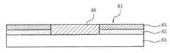
본 발명의 또다른 실시예에서는, 저항이 충진될 부분에 도금이 되지 않도록 하는 도금 레지스트 패턴을 형성하고 그 주위에만 도금을 한 후에, 그 위에 에칭레지스트를 선택적으로 형성한 후, 도금 레지스트 패턴을 제거하고 에칭에 의해 도금 레지스트가 없는 부분의 동박층을 제거한 후에 저항 페이스트를 충진하여 저항을 형성한다. 도8a 내지 도8h는 이러한 본 발명에 따른 실시예를 나타낸다.In another embodiment of the present invention, after forming a plating resist pattern to prevent plating on the portion to be filled with resistance and plating only around it, an etching resist is selectively formed thereon, and then the plating resist pattern is removed. After removing the copper foil layer in the portion without the plating resist by etching, a resistor paste is filled to form a resistance. 8a to 8h show such an embodiment according to the present invention.
도8a는 베이스 기판으로 사용되는 동박 적층판(81)의 단면을 나타낸다. 보강 기재(83)에 동박층(82)이 입혀져 있다. 동박적층판(81)에는 여러 가지 종류가 있으나 유리 섬유에 에폭시 수지를 침투시킨 보강 기재에 동박을 입힌 소위 FR-4 동박 적층판을 사용하는 것이 바람직하다.8A shows a cross section of a copper foil laminated
도8b에서, 동박 적층판(81)의 동박층(82) 위에 저항이 삽입될 부분에 해당하는 도금 레지스트 패턴(84)을 형성한다. 도9a는 이와 같이 도금 레지스트 패턴(84)이 형성된 동박(82)의 사시도를 나타낸다.In FIG. 8B, a plating resist
도8c에서, 도금에 의해 동도금층(85)을 형성한다. 도금 레지스트 패턴(84)이 형성되어 있는 부분에는 도금이 이루어지지 않는다.In Fig. 8C, a
도8d에서, 박리액을 사용하여 도금 레지스트 패턴(84)을 제거한다.In Fig. 8D, the plating resist
도8e에서, 저항 페이스트가 충진될 부분 이외의 부분에 에칭 레지스트 패턴(86)을 형성한다. 에칭 레지스트로는 다양한 물질을 사용할 수 있으나, Sn 도금을 사용하는 것이 가장 바람직하다.In Fig. 8E, an etching resist
도8f에서, 에칭에 의해 동박층(82) 중 저항 페이스트가 충진될 부분의 동박층을 제거한다.In Fig. 8F, the copper foil layer of the portion of the
도8g에서, 인쇄기를 사용하여 동박이 제거된 부분에 동박과 거의 같은 높이 가 되도록 저항 페이스트(88)를 충진한다. 이때, 상기 저항 페이스트로는 카본 블랙과 같은 입자에 고분자를 메트릭스로 하는 카본계 저항 페이스트를 사용하는 것이 바람직하다.In Fig. 8G, the resist
통상적인 스크린 인쇄기를 이용하여 충진하는 것도 가능하지만, 저항 편차를 줄이고 보이드 형성을 방지하기 위해서는 진공 인쇄기를 사용하여 충진하는 것이 바람직하다. 그리고 나서, 충진된 저항 페이스트(88)를 약 150∼250℃에서 가열 건조하여 열경화시킨다.It is also possible to fill using a conventional screen printing machine, but in order to reduce resistance variation and prevent void formation, it is preferable to fill using a vacuum printing machine. Then, the filled
도8h에서, 연마 가공에 의해 동박에 비해 위로 돌출된 저항 페이스트를 제거하여 저항 페이스트(88)가 다른 동박과 같은 높이가 되도록 한다. 도9b는 이와 같이 저항 페이스트(86)가 다른 동박과 같은 높이가 되도록 연마 가공된 동박(82)의 사시도를 나타낸다.In Fig. 8H, the resistive paste protruding upward relative to the copper foil by polishing is removed so that the resist
실시예에 따라서는, 저항 페이스트의 전기 접점 부위에 저항의 접점을 확보하기 위해 전도성이 우수한 은, 금, 백금, 니켈 등의 금속층을 덧붙일 수 있다. 또한 접점부위의 형태를 접점면적을 넓히기 위해 여러 가지 모양으로 변형할 수 있다. 접점부에 덧붙여진 금속층은 추후에 회로 패턴이 형성되고 각종 소자가 연결되어 회로가 구성될 때, 매립된 저항의 접촉 저항 편차를 감소시키는 역할을 하게 된다.In some embodiments, metal layers such as silver, gold, platinum, and nickel having excellent conductivity may be added to secure the contact of the resistor to the electrical contact portion of the resistor paste. In addition, the shape of the contact portion can be modified into various shapes to increase the contact area. The metal layer added to the contact portion serves to reduce contact resistance variation of the embedded resistor when a circuit pattern is formed later and various elements are connected to form a circuit.
또한, 실시예에 따라서는 도8h의 연마가공까지 완료된 기판에 도6e 또는 도7d와 유사하게 금속층을 추가적으로 도금하여 매립 저항이 인쇄회로기판 내에 완전히 매립되도록 하는 것도 가능하다.Further, according to the embodiment, it is also possible to additionally plate the metal layer on the substrate completed by the polishing process of FIG. 8H similarly to FIG. 6E or 7D so that the buried resistor is completely embedded in the printed circuit board.
본 발명의 매립된 저항을 갖는 인쇄회로기판 제조 방법에 따르면, 종래방법에 비해 스크린 프린팅의 정밀도에 크게 좌우되지 않고, 종래의 스크린 프린팅에 사용되는 고가의 스크린 망사를 사용하지 않아도 되므로 작업성이 매우 향상된다.According to the method of manufacturing a printed circuit board having a buried resistor of the present invention, it is not greatly influenced by the precision of screen printing compared to the conventional method, and it is not necessary to use expensive screen mesh used for conventional screen printing. Is improved.
또한, 본 발명의 매립된 저항을 갖는 인쇄회로기판 제조 방법에 따르면, 인쇄회로기판에 도포되는 저항의 두께가 인쇄장비의 위치에 따라 좌우되지 않고, 동박층의 두께에 따라 좌우되므로 도포두께를 보다 균일하게 형성할 수 있다.In addition, according to the method of manufacturing a printed circuit board having a buried resistance of the present invention, the thickness of the resistance applied to the printed circuit board does not depend on the position of the printing equipment, but depends on the thickness of the copper foil layer, the coating thickness is more. It can form uniformly.
또한, 본 발명의 매립된 저항을 갖는 인쇄회로기판 제조 방법에 따르면, 형성된 저항이 주위의 동박 표면과 일치하므로, 적층을 하는 경우 압력에 의한 변형이 없어 적층 후 저항값 변화량이 일정하게 유지될 수 있다.In addition, according to the method of manufacturing a printed circuit board having a buried resistance of the present invention, since the formed resistance coincides with the surrounding copper foil surface, there is no deformation due to pressure in the case of lamination, and thus the change in resistance value after lamination can be kept constant. have.
또한, 본 발명의 매립된 저항을 갖는 인쇄회로기판 제조 방법에 따르면, 레이저 트리밍 공정 없이도 원하는 저항값을 형성할 수 있다In addition, according to the method of manufacturing a printed circuit board having a buried resistor of the present invention, a desired resistance value can be formed without a laser trimming process.
또한, 본 발명의 매립된 저항을 갖는 인쇄회로기판 제조 방법에 따르면, 저항 연결을 위한 별도의 패드 없이 저항을 전기적으로 연결할 수 있는 인쇄회로기판을 제공할 수 있다.In addition, according to the method of manufacturing a printed circuit board having a buried resistor of the present invention, it is possible to provide a printed circuit board capable of electrically connecting a resistor without a separate pad for resistance connection.
또한, 본 발명의 매립된 저항을 갖는 인쇄회로기판 제조 방법에 따른 인쇄회로기판은, 저항이 인쇄회로기판의 내부에 삽입되므로 단위면적당 부품밀도가 증가되어, 고집적 전자기기에 사용될 수 있다.In addition, the printed circuit board according to the method of manufacturing a printed circuit board with embedded resistance of the present invention, since the resistance is inserted into the printed circuit board, the component density per unit area is increased, it can be used in a highly integrated electronic device.
또한, 본 발명의 매립된 저항을 갖는 인쇄회로기판 제조 방법에 따르면 진공 인쇄를 통해 저항 페이스트에 보이드(void) 형성을 억제하여 더욱 정밀한 저항값을 얻을 수 있다.In addition, according to the method of manufacturing a printed circuit board having a buried resistor of the present invention, it is possible to obtain a more precise resistance value by suppressing void formation in the resistor paste through vacuum printing.
또한, 본 발명의 매립된 저항을 갖는 인쇄회로기판 제조 방법은, 인쇄회로기판 내에서 저항의 위치에 따른 편차가 거의 없어 제조 공정의 신뢰성이 확보된다.In addition, the printed circuit board manufacturing method having the embedded resistor of the present invention has almost no variation in the resistance position in the printed circuit board, thereby ensuring the reliability of the manufacturing process.
또한, 본 발명의 매립된 저항을 갖는 인쇄회로기판 제조 방법에 따르면 회로의 외곽 뿐만 아니라 내부 어느 층에도 매립 저항을 형성할 수 있고, 내부에 저항을 형성하는 경우에는 프레스 공정 등의 경우에도 저항 파손의 우려가 최소화 된다.In addition, according to the method of manufacturing a printed circuit board having a buried resistor of the present invention, a buried resistor can be formed not only on the outside of the circuit but also on any layer inside, and in the case of forming a resistor therein, the resistance is broken even in the press process or the like. Concerns are minimized.
Claims (16)
Translated fromKoreanPriority Applications (4)
| Application Number | Priority Date | Filing Date | Title |
|---|---|---|---|
| KR1020030077949AKR100754065B1 (en) | 2003-11-05 | 2003-11-05 | Method of manufacturing printed circuit board with embedded resistor |
| US10/770,806US7284317B2 (en) | 2003-11-05 | 2004-02-03 | Method of producing printed circuit board with embedded resistor |
| JP2004035354AJP2005142523A (en) | 2003-11-05 | 2004-02-12 | Method of manufacturing printed circuit board including buried resistor |
| CNB2004100078623ACN100438723C (en) | 2003-11-05 | 2004-03-03 | Manufacture of PCB with resistors embedded |
Applications Claiming Priority (1)
| Application Number | Priority Date | Filing Date | Title |
|---|---|---|---|
| KR1020030077949AKR100754065B1 (en) | 2003-11-05 | 2003-11-05 | Method of manufacturing printed circuit board with embedded resistor |
Publications (2)
| Publication Number | Publication Date |
|---|---|
| KR20050043157A KR20050043157A (en) | 2005-05-11 |
| KR100754065B1true KR100754065B1 (en) | 2007-08-31 |
Family
ID=34698354
Family Applications (1)
| Application Number | Title | Priority Date | Filing Date |
|---|---|---|---|
| KR1020030077949AExpired - Fee RelatedKR100754065B1 (en) | 2003-11-05 | 2003-11-05 | Method of manufacturing printed circuit board with embedded resistor |
Country Status (4)
| Country | Link |
|---|---|
| US (1) | US7284317B2 (en) |
| JP (1) | JP2005142523A (en) |
| KR (1) | KR100754065B1 (en) |
| CN (1) | CN100438723C (en) |
Families Citing this family (39)
| Publication number | Priority date | Publication date | Assignee | Title |
|---|---|---|---|---|
| KR100585203B1 (en)* | 2004-02-27 | 2006-06-01 | 대덕전자 주식회사 | Method of manufacturing a buried resistor in a printed circuit board |
| KR100598274B1 (en)* | 2004-09-01 | 2006-07-07 | 삼성전기주식회사 | Resistor-embedded printed circuit board and manufacturing method thereof |
| US8501575B2 (en)* | 2005-01-10 | 2013-08-06 | Endicott Interconnect Technologies, Inc. | Method of forming multilayer capacitors in a printed circuit substrate |
| JP4661351B2 (en)* | 2005-05-19 | 2011-03-30 | 凸版印刷株式会社 | Passive element built-in wiring board and manufacturing method thereof |
| DE102005047090A1 (en)* | 2005-09-30 | 2007-04-05 | Robert Bosch Gmbh | Electric device for conductor plate has connectors made from metal layer applied to support each with bay-type shape so that resistance material can be inserted between same |
| KR100754805B1 (en)* | 2006-01-25 | 2007-09-03 | 삼성전기주식회사 | Printed circuit board with embedded resistor and manufacturing method thereof |
| US7605343B2 (en)* | 2006-05-24 | 2009-10-20 | Electro Scientific Industries, Inc. | Micromachining with short-pulsed, solid-state UV laser |
| KR100776685B1 (en) | 2006-08-07 | 2007-11-16 | 대덕전자 주식회사 | Embedded printed circuit board with flat carbon resistance and manufacturing method |
| WO2008151181A1 (en)* | 2007-06-04 | 2008-12-11 | Lear Corporation | Battery post connector |
| US8476864B2 (en)* | 2007-06-13 | 2013-07-02 | Lear Corporation | Battery monitoring system |
| CN101600298B (en)* | 2009-07-09 | 2011-01-12 | 皆利士多层线路版(中山)有限公司 | Manufacturing method of circuit board |
| US20110127249A1 (en)* | 2009-11-27 | 2011-06-02 | Hotronic International Limited | Electric heating element for insoles |
| DE102010030070A1 (en)* | 2010-06-15 | 2012-02-02 | Robert Bosch Gmbh | Method for producing an electrical connection and electrical connection |
| JP6054382B2 (en) | 2011-06-16 | 2016-12-27 | レスメド・リミテッドResMed Limited | Humidifier and layered heating element |
| CN102573284A (en)* | 2011-12-30 | 2012-07-11 | 广东生益科技股份有限公司 | Flexible light strip and manufacturing method thereof |
| CN103037622B (en)* | 2013-01-05 | 2015-08-12 | 上海卓凯电子科技有限公司 | There is the circuit board of built-in type resistance |
| WO2014106331A1 (en)* | 2013-01-05 | 2014-07-10 | 上海卓凯电子科技有限公司 | Circuit board with buried resistor |
| US9786354B2 (en) | 2013-07-10 | 2017-10-10 | Samsung Electronics Co., Ltd. | Memory module |
| CN104582264B (en)* | 2013-10-14 | 2018-01-26 | 珠海方正科技高密电子有限公司 | A method of making printed device, printed cover plate and printed circuit board |
| US9521752B2 (en)* | 2014-09-19 | 2016-12-13 | Harris Corporation | Method of making an electronic device having a thin film resistor formed on an LCP solder mask and related devices |
| WO2016073686A1 (en) | 2014-11-06 | 2016-05-12 | The Procter & Gamble Company | Zonal patterned apertured webs, laminates, and methods for making the same |
| EP3215086B1 (en) | 2014-11-06 | 2020-03-18 | The Procter and Gamble Company | Crimped fiber spunbond nonwoven webs / laminates |
| CN104902690B (en)* | 2015-05-26 | 2017-12-15 | 广州杰赛科技股份有限公司 | A kind of preparation method of circuit board |
| CN105307393B (en)* | 2015-11-13 | 2017-12-19 | 惠州市金百泽电路科技有限公司 | A kind of manufacture craft for lifting electric conductive carbon printing printed circuit board resistance accuracy |
| US9763329B1 (en) | 2016-03-11 | 2017-09-12 | Apple Inc. | Techniques for observing an entire communication bus in operation |
| EP4056158B1 (en) | 2017-02-16 | 2024-03-06 | The Procter & Gamble Company | Absorbent articles with substrates having repeating patterns of apertures comprising a plurality of repeat units |
| CN107770959A (en)* | 2017-09-28 | 2018-03-06 | 衢州顺络电路板有限公司 | The printed wiring board and its manufacture method of embedded resistors design |
| CN108495485A (en)* | 2018-04-09 | 2018-09-04 | 陈长生 | A kind of multilayer board insertion resistance production method |
| US12127925B2 (en) | 2018-04-17 | 2024-10-29 | The Procter & Gamble Company | Webs for absorbent articles and methods of making the same |
| TWI713424B (en)* | 2018-10-15 | 2020-12-11 | 鼎展電子股份有限公司 | Copper film with buried film resistor and printed circuit board having the same |
| CN112584614A (en)* | 2019-09-27 | 2021-03-30 | 深南电路股份有限公司 | Manufacturing method of buried resistance circuit board and buried resistance circuit board |
| CN113853069A (en)* | 2020-06-28 | 2021-12-28 | 庆鼎精密电子(淮安)有限公司 | Manufacturing method of circuit board intermediate, circuit board and manufacturing method thereof |
| CN112533395B (en)* | 2020-12-21 | 2021-12-24 | 北京同方信息安全技术股份有限公司 | Method for embedding resistor in printed circuit board and printed circuit board thereof |
| CN112802646B (en)* | 2021-01-14 | 2025-06-03 | 广东风华高新科技股份有限公司 | A method for preparing a chip alloy resistor |
| CN112867270B (en)* | 2021-02-02 | 2023-01-24 | 沪士电子股份有限公司 | A method of printing a high-speed circuit board using conductive paste and the high-speed circuit board |
| CN114245601A (en)* | 2021-12-01 | 2022-03-25 | 惠州市金百泽电路科技有限公司 | High-precision carbon oil resistance value manufacturing method of circuit board |
| CN114501864B (en)* | 2022-04-14 | 2022-07-01 | 四川英创力电子科技股份有限公司 | A method of manufacturing an embedded resistor printed circuit board |
| CN115379672A (en)* | 2022-08-26 | 2022-11-22 | 宁波华远电子科技有限公司 | Soft-hard combined packaging structure of embedded component and preparation method thereof |
| CN119029584A (en)* | 2024-08-08 | 2024-11-26 | 深圳市爱特姆科技有限公司 | Connector and manufacturing process thereof |
Citations (2)
| Publication number | Priority date | Publication date | Assignee | Title |
|---|---|---|---|---|
| JP2002133945A (en)* | 2000-10-30 | 2002-05-10 | Mitsubishi Electric Corp | Resistor paste and printed wiring board using the same |
| JP2002280699A (en)* | 2001-03-16 | 2002-09-27 | Mitsubishi Electric Corp | Method of forming resistor on printed circuit board |
Family Cites Families (18)
| Publication number | Priority date | Publication date | Assignee | Title |
|---|---|---|---|---|
| JPS58107694A (en) | 1981-12-21 | 1983-06-27 | 株式会社日立製作所 | Hybrid integrated circuit and method of producing same |
| JPS63110692A (en) | 1986-10-28 | 1988-05-16 | 日本シイエムケイ株式会社 | Manufacturing method of printed wiring board |
| US4892776A (en) | 1987-09-02 | 1990-01-09 | Ohmega Electronics, Inc. | Circuit board material and electroplating bath for the production thereof |
| JPH0787261B2 (en) | 1988-08-25 | 1995-09-20 | 株式会社村田製作所 | Copper clad laminate |
| JPH02103993A (en) | 1988-10-13 | 1990-04-17 | Matsushita Electric Ind Co Ltd | Manufacturing method of printed wiring board |
| US5043695A (en)* | 1990-06-15 | 1991-08-27 | Bourns, Inc. | Housing assembly for miniature electronic device |
| JP2828325B2 (en) | 1990-07-11 | 1998-11-25 | ローム株式会社 | Manufacturing method of thermal head |
| JPH04127599A (en) | 1990-09-19 | 1992-04-28 | Fujitsu Ltd | Input-output electronic equipment container |
| JPH04145694A (en) | 1990-10-05 | 1992-05-19 | Japan Radio Co Ltd | Electrode structure of printed resistor in resin multilayer printed board |
| ES2105000T3 (en) | 1992-05-12 | 1997-10-16 | Siemens Ag | PRINTED CIRCUIT BOARD WITH MULTIPLE LAYERS. |
| JPH07106729A (en) | 1993-09-30 | 1995-04-21 | Murata Mfg Co Ltd | Manufacture of thick film circuit component |
| US5624782A (en)* | 1994-04-14 | 1997-04-29 | E. I. Du Pont De Nemours And Company | Method of manufacturing thick-film resistor elements |
| JP3655026B2 (en) | 1996-10-01 | 2005-06-02 | 松下電器産業株式会社 | Method for forming thick film pattern |
| EP0848585A1 (en) | 1996-12-13 | 1998-06-17 | Macdermid Incorporated | Process for the manufacture of printed circuit boards with plated resistors |
| US6171921B1 (en)* | 1998-06-05 | 2001-01-09 | Motorola, Inc. | Method for forming a thick-film resistor and thick-film resistor formed thereby |
| JP3203345B2 (en) | 1999-01-08 | 2001-08-27 | サンユレック株式会社 | Vacuum printing apparatus and vacuum printing method |
| TW444522B (en)* | 1999-06-03 | 2001-07-01 | Ind Tech Res Inst | Process for forming polymer thick film resistors and metal thin film resistors in a printed circuited substrate |
| KR100463434B1 (en)* | 2001-12-04 | 2004-12-23 | 삼성전기주식회사 | Printed Circuit Board with Buried Resistors and Manufacturing Method Thereof |
- 2003
- 2003-11-05KRKR1020030077949Apatent/KR100754065B1/ennot_activeExpired - Fee Related
- 2004
- 2004-02-03USUS10/770,806patent/US7284317B2/ennot_activeExpired - Fee Related
- 2004-02-12JPJP2004035354Apatent/JP2005142523A/enactivePending
- 2004-03-03CNCNB2004100078623Apatent/CN100438723C/ennot_activeExpired - Fee Related
Patent Citations (2)
| Publication number | Priority date | Publication date | Assignee | Title |
|---|---|---|---|---|
| JP2002133945A (en)* | 2000-10-30 | 2002-05-10 | Mitsubishi Electric Corp | Resistor paste and printed wiring board using the same |
| JP2002280699A (en)* | 2001-03-16 | 2002-09-27 | Mitsubishi Electric Corp | Method of forming resistor on printed circuit board |
Also Published As
| Publication number | Publication date |
|---|---|
| CN100438723C (en) | 2008-11-26 |
| KR20050043157A (en) | 2005-05-11 |
| JP2005142523A (en) | 2005-06-02 |
| CN1615070A (en) | 2005-05-11 |
| US7284317B2 (en) | 2007-10-23 |
| US20050175385A1 (en) | 2005-08-11 |
Similar Documents
| Publication | Publication Date | Title |
|---|---|---|
| KR100754065B1 (en) | Method of manufacturing printed circuit board with embedded resistor | |
| TWI423745B (en) | Wiring board with built-in component and method for manufacturing the same | |
| JP4000143B2 (en) | Printed circuit board having a high dielectric constant capacitor and manufacturing method thereof | |
| JP3910045B2 (en) | Method for manufacturing electronic component internal wiring board | |
| US20090101400A1 (en) | Method for manufacturing component-embedded substrate and component-embedded substrate | |
| US6898850B2 (en) | Method of manufacturing circuit board and communication appliance | |
| JPS62299097A (en) | Wiring board | |
| JP2004363434A (en) | Electronic circuit device and method of manufacturing the same | |
| EP0384927B1 (en) | Molded circuit board | |
| US6218736B1 (en) | Circuit board and semiconductor device, and method of manufacturing the same | |
| KR20080061816A (en) | Printed circuit board and manufacturing method thereof | |
| KR100733251B1 (en) | Printed circuit board with double electronic parts and manufacturing method | |
| KR101018281B1 (en) | Passive element embedded printed circuit board manufacturing method | |
| KR20100117975A (en) | Embedded circuit board and method of manufacturing the same | |
| KR100747020B1 (en) | Resistor-embedded printed circuit board and its manufacturing method | |
| KR100909684B1 (en) | Manufacturing method of resistance mounted flexible printed circuit board | |
| JP3440786B2 (en) | Printed wiring board | |
| KR100483623B1 (en) | Printed circuit board with buried resistor, preparing and optimizing method for the same | |
| KR100642047B1 (en) | Built-in resistor manufacturing method and printed circuit board manufacturing method using the same | |
| JP3846209B2 (en) | Multilayer printed wiring board manufacturing method and multilayer printed wiring board | |
| KR100932535B1 (en) | Printed circuit board with embedded resistor and manufacturing method | |
| KR100754805B1 (en) | Printed circuit board with embedded resistor and manufacturing method thereof | |
| KR20080034691A (en) | Capacitor, Manufacturing Method and Printed Circuit Board with Capacitor | |
| JPS6153852B2 (en) | ||
| KR100690354B1 (en) | Thermosetting Thick Film Resistor Manufacturing Method and Resistor |
Legal Events
| Date | Code | Title | Description |
|---|---|---|---|
| A201 | Request for examination | ||
| PA0109 | Patent application | St.27 status event code:A-0-1-A10-A12-nap-PA0109 | |
| PA0201 | Request for examination | St.27 status event code:A-1-2-D10-D11-exm-PA0201 | |
| R18-X000 | Changes to party contact information recorded | St.27 status event code:A-3-3-R10-R18-oth-X000 | |
| D13-X000 | Search requested | St.27 status event code:A-1-2-D10-D13-srh-X000 | |
| PG1501 | Laying open of application | St.27 status event code:A-1-1-Q10-Q12-nap-PG1501 | |
| D14-X000 | Search report completed | St.27 status event code:A-1-2-D10-D14-srh-X000 | |
| E902 | Notification of reason for refusal | ||
| PE0902 | Notice of grounds for rejection | St.27 status event code:A-1-2-D10-D21-exm-PE0902 | |
| AMND | Amendment | ||
| P11-X000 | Amendment of application requested | St.27 status event code:A-2-2-P10-P11-nap-X000 | |
| P13-X000 | Application amended | St.27 status event code:A-2-2-P10-P13-nap-X000 | |
| E601 | Decision to refuse application | ||
| PE0601 | Decision on rejection of patent | St.27 status event code:N-2-6-B10-B15-exm-PE0601 | |
| J201 | Request for trial against refusal decision | ||
| PJ0201 | Trial against decision of rejection | St.27 status event code:A-3-3-V10-V11-apl-PJ0201 | |
| AMND | Amendment | ||
| P11-X000 | Amendment of application requested | St.27 status event code:A-2-2-P10-P11-nap-X000 | |
| P13-X000 | Application amended | St.27 status event code:A-2-2-P10-P13-nap-X000 | |
| PB0901 | Examination by re-examination before a trial | St.27 status event code:A-6-3-E10-E12-rex-PB0901 | |
| E801 | Decision on dismissal of amendment | ||
| B601 | Maintenance of original decision after re-examination before a trial | ||
| PB0601 | Maintenance of original decision after re-examination before a trial | St.27 status event code:N-3-6-B10-B17-rex-PB0601 | |
| R18-X000 | Changes to party contact information recorded | St.27 status event code:A-3-3-R10-R18-oth-X000 | |
| J301 | Trial decision | Free format text:TRIAL DECISION FOR APPEAL AGAINST DECISION TO DECLINE REFUSAL REQUESTED 20060313 Effective date:20070528 | |
| PJ1301 | Trial decision | St.27 status event code:A-3-3-V10-V15-crt-PJ1301 Decision date:20070528 Appeal event data comment text:Appeal Kind Category : Appeal against decision to decline refusal, Appeal Ground Text : 2003 0077949 Appeal request date:20060313 Appellate body name:Patent Examination Board Decision authority category:Office appeal board Decision identifier:2006101002210 | |
| PS0901 | Examination by remand of revocation | St.27 status event code:A-6-3-E10-E12-rex-PS0901 | |
| S901 | Examination by remand of revocation | ||
| GRNO | Decision to grant (after opposition) | ||
| PS0701 | Decision of registration after remand of revocation | St.27 status event code:A-3-4-F10-F13-rex-PS0701 | |
| GRNT | Written decision to grant | ||
| PR0701 | Registration of establishment | St.27 status event code:A-2-4-F10-F11-exm-PR0701 | |
| PR1002 | Payment of registration fee | St.27 status event code:A-2-2-U10-U11-oth-PR1002 Fee payment year number:1 | |
| PG1601 | Publication of registration | St.27 status event code:A-4-4-Q10-Q13-nap-PG1601 | |
| G170 | Re-publication after modification of scope of protection [patent] | ||
| PG1701 | Publication of correction | St.27 status event code:A-5-5-P10-P19-oth-PG1701 Patent document republication publication date:20080418 Republication note text:Request for Correction Notice (Document Request) Gazette number:1007540650000 Gazette reference publication date:20070831 | |
| PR1001 | Payment of annual fee | St.27 status event code:A-4-4-U10-U11-oth-PR1001 Fee payment year number:4 | |
| FPAY | Annual fee payment | Payment date:20110711 Year of fee payment:5 | |
| PR1001 | Payment of annual fee | St.27 status event code:A-4-4-U10-U11-oth-PR1001 Fee payment year number:5 | |
| LAPS | Lapse due to unpaid annual fee | ||
| PC1903 | Unpaid annual fee | St.27 status event code:A-4-4-U10-U13-oth-PC1903 Not in force date:20120825 Payment event data comment text:Termination Category : DEFAULT_OF_REGISTRATION_FEE | |
| PC1903 | Unpaid annual fee | St.27 status event code:N-4-6-H10-H13-oth-PC1903 Ip right cessation event data comment text:Termination Category : DEFAULT_OF_REGISTRATION_FEE Not in force date:20120825 | |
| R18-X000 | Changes to party contact information recorded | St.27 status event code:A-5-5-R10-R18-oth-X000 | |
| R18-X000 | Changes to party contact information recorded | St.27 status event code:A-5-5-R10-R18-oth-X000 |