KR100753365B1 - Shift register and liquid crystal display device having same - Google Patents
Shift register and liquid crystal display device having sameDownload PDFInfo
- Publication number
- KR100753365B1 KR100753365B1KR1020010063800AKR20010063800AKR100753365B1KR 100753365 B1KR100753365 B1KR 100753365B1KR 1020010063800 AKR1020010063800 AKR 1020010063800AKR 20010063800 AKR20010063800 AKR 20010063800AKR 100753365 B1KR100753365 B1KR 100753365B1
- Authority
- KR
- South Korea
- Prior art keywords
- node
- terminal
- signal
- gate
- output
- Prior art date
- Legal status (The legal status is an assumption and is not a legal conclusion. Google has not performed a legal analysis and makes no representation as to the accuracy of the status listed.)
- Expired - Fee Related
Links
Images


Classifications
- G—PHYSICS
- G09—EDUCATION; CRYPTOGRAPHY; DISPLAY; ADVERTISING; SEALS
- G09G—ARRANGEMENTS OR CIRCUITS FOR CONTROL OF INDICATING DEVICES USING STATIC MEANS TO PRESENT VARIABLE INFORMATION
- G09G3/00—Control arrangements or circuits, of interest only in connection with visual indicators other than cathode-ray tubes
- G09G3/20—Control arrangements or circuits, of interest only in connection with visual indicators other than cathode-ray tubes for presentation of an assembly of a number of characters, e.g. a page, by composing the assembly by combination of individual elements arranged in a matrix no fixed position being assigned to or needed to be assigned to the individual characters or partial characters
- G09G3/34—Control arrangements or circuits, of interest only in connection with visual indicators other than cathode-ray tubes for presentation of an assembly of a number of characters, e.g. a page, by composing the assembly by combination of individual elements arranged in a matrix no fixed position being assigned to or needed to be assigned to the individual characters or partial characters by control of light from an independent source
- G09G3/36—Control arrangements or circuits, of interest only in connection with visual indicators other than cathode-ray tubes for presentation of an assembly of a number of characters, e.g. a page, by composing the assembly by combination of individual elements arranged in a matrix no fixed position being assigned to or needed to be assigned to the individual characters or partial characters by control of light from an independent source using liquid crystals
- G—PHYSICS
- G11—INFORMATION STORAGE
- G11C—STATIC STORES
- G11C19/00—Digital stores in which the information is moved stepwise, e.g. shift registers
- G11C19/28—Digital stores in which the information is moved stepwise, e.g. shift registers using semiconductor elements
- G11C19/282—Digital stores in which the information is moved stepwise, e.g. shift registers using semiconductor elements with charge storage in a depletion layer, i.e. charge coupled devices [CCD]
- G11C19/285—Peripheral circuits, e.g. for writing into the first stage; for reading-out of the last stage
- G—PHYSICS
- G11—INFORMATION STORAGE
- G11C—STATIC STORES
- G11C19/00—Digital stores in which the information is moved stepwise, e.g. shift registers
- G—PHYSICS
- G09—EDUCATION; CRYPTOGRAPHY; DISPLAY; ADVERTISING; SEALS
- G09G—ARRANGEMENTS OR CIRCUITS FOR CONTROL OF INDICATING DEVICES USING STATIC MEANS TO PRESENT VARIABLE INFORMATION
- G09G3/00—Control arrangements or circuits, of interest only in connection with visual indicators other than cathode-ray tubes
- G09G3/20—Control arrangements or circuits, of interest only in connection with visual indicators other than cathode-ray tubes for presentation of an assembly of a number of characters, e.g. a page, by composing the assembly by combination of individual elements arranged in a matrix no fixed position being assigned to or needed to be assigned to the individual characters or partial characters
- G09G3/34—Control arrangements or circuits, of interest only in connection with visual indicators other than cathode-ray tubes for presentation of an assembly of a number of characters, e.g. a page, by composing the assembly by combination of individual elements arranged in a matrix no fixed position being assigned to or needed to be assigned to the individual characters or partial characters by control of light from an independent source
- G09G3/36—Control arrangements or circuits, of interest only in connection with visual indicators other than cathode-ray tubes for presentation of an assembly of a number of characters, e.g. a page, by composing the assembly by combination of individual elements arranged in a matrix no fixed position being assigned to or needed to be assigned to the individual characters or partial characters by control of light from an independent source using liquid crystals
- G09G3/3611—Control of matrices with row and column drivers
Landscapes
- Engineering & Computer Science (AREA)
- Chemical & Material Sciences (AREA)
- Crystallography & Structural Chemistry (AREA)
- Physics & Mathematics (AREA)
- Computer Hardware Design (AREA)
- General Physics & Mathematics (AREA)
- Theoretical Computer Science (AREA)
- Control Of Indicators Other Than Cathode Ray Tubes (AREA)
- Shift Register Type Memory (AREA)
- Liquid Crystal Display Device Control (AREA)
Abstract
Translated fromKoreanDescription
Translated fromKorean도 1은 일반적인 폴리 실리콘 TFT LCD의 TFT 기판의 구성도이다.1 is a configuration diagram of a TFT substrate of a general polysilicon TFT LCD.
도 2는 본 발명에 의한 쉬프트 레지스터의 블록 구성도이다.2 is a block diagram of a shift register according to the present invention.
도 3은 본 발명에 의한 쉬프트 레지스터의 각 스테이지의 바람직한 일 실시예의 회로도이다.3 is a circuit diagram of one preferred embodiment of each stage of a shift register according to the present invention.
도 4 및 도 5는 도 3의 각부 타이밍도이다.4 and 5 are timing diagrams of the parts of FIG. 3.
도 6은 본 발명에 의한 쉬프트 레지스터의 각 스테이지의 바람직한 다른 실시예의 회로도이다.Fig. 6 is a circuit diagram of another preferred embodiment of each stage of the shift register according to the present invention.
도 7은 도 3에 도시된 본 발명의 쉬프트 레지스터의 비교예로서의 쉬프트 레지스터의 블록 구성도이다.7 is a block diagram of a shift register as a comparative example of the shift register of the present invention shown in FIG.
도 8은 도 7에 도시된 쉬프트 레지스터의 각 스테이지의 회로도이다FIG. 8 is a circuit diagram of each stage of the shift register shown in FIG.
도 9 및 도 10은 도 8의 각부 타이밍도이다.9 and 10 are timing diagrams of each part of FIG. 8.
도 11은 본 발명의 쉬프트레지스터와 비교예의 쉬프트레지스터의 전력소모를 비교한 그래프이다.11 is a graph comparing the power consumption of the shift register of the present invention and the shift register of the comparative example.
*도면의 주요 부분에 대한 간략한 부호의 설명** Description of abbreviated symbols for the main parts of the drawings *
10 : TFT기판10: TFT substrate
20 : 필름 케이블20: film cable
30 : 통합회로기판30: integrated circuit board
100 : 표시 셀 어레이100: display cell array
110 : 게이트선구동회로110: gate line driving circuit
120 : 신호선 구동회로120: signal line driver circuit
130 : 외부연결단자130: external connection terminal
200, 300 : 쉬프트 레지스터200, 300: shift register
210, 310 : 입력회로210, 310: input circuit
220, 320 : 레벨쉬프터220, 320: Level shifter
222, 322, 323 : 레벨쉬프트부222, 322, 323: level shift unit
224, 324 : 래치부224, 324: latch portion
230, 330 : 제 1 출력회로230, 330: first output circuit
240, 340 : 제 2 출력회로240, 340: second output circuit
PM1~PM5 : 피모스 트랜지스터PM1 ~ PM5: PMOS transistor
NM1~NM4 : 엔모스 트랜지스터NM1 ~ NM4: NMOS transistor
INV, INV1~INV4 ; 인버터INV, INV1 to INV4; inverter
NOR : 노아 게이트NOR: Noah Gate
SRC, NSRC : 스테이지SRC, NSRC: Stage
본 발명은 쉬프트 레지스터 및 액정표시장치에 관한 것으로, 특히 액정표시장치에 있어서 게이트 구동회로 및 신호선 구동회로의 쉬프트 레지스터의 소비전력을 줄일 수 있는 쉬프트 레지스터의 회로 개선에 것에 관한 것이다.BACKGROUND OF THE
일반적으로 액정표시장치는 화면의 주사선을 차례로 선택하고 선택된 주사선 상의 모든 화소들 각가의 TFT(Thin Film Transister)와 같은 스위칭 소자를 턴온시켜서 동시에 각각의 신호를 인가하는 액티브 매트릭스(Active Matrix) 구동방법을 사용한다.In general, a liquid crystal display device uses an active matrix driving method in which a scanning line of a screen is sequentially selected and a switching element such as a thin film transistor (TFT) of all pixels on the selected scanning line is turned on to simultaneously apply respective signals. use.
TFT-AM LCD는 투과형인 경우에 액정패널, 구동부, 백라이트 유닛을 포함하고, 반사형의 경우에는 백라이트 유닛 대신에 반사판을 구비한다.The TFT-AM LCD includes a liquid crystal panel, a driver, and a backlight unit in the case of the transmissive type, and includes a reflecting plate in place of the backlight unit in the case of the reflective type.
투과형 LCD의 경우에는 공급전력의 대부분이 백라이트 유닛에서 약 70% 정도 소비되고, 약 10%정도가 신호처리를 수행하는 제어부에서 소비되며, 신호선 구동 LSI 내부에서 약 10% 정도가 소비되고, 신호선 충반전에 약 4%정도 소비되는 것으로 알려져 있다.In the case of the transmissive LCD, most of the power supply is consumed by about 70% in the backlight unit, about 10% is consumed by the control unit performing signal processing, and about 10% is consumed inside the signal line driving LSI. It is known that about 4% is spent in reversal.
따라서, LCD에서 소비전력을 낮추기 위하여 백라이트의 고효율화, 구동회로의 저소비 전력화, 액정 패널의 고투과율 등의 세가지 방향에서의 기술 개발이 활발히 진행되고 있다.Accordingly, in order to lower power consumption in LCDs, technologies are being actively developed in three directions such as high efficiency of backlight, low power consumption of driving circuit, and high transmittance of liquid crystal panel.
구동회로의 저소비 전력화를 위하여 a-Si TFT LCD 기술에서 poly-Si 소자 기술이 관심을 끌고 있다. 폴리 실리콘 소자는 아몰퍼스 실리콘에 비해 캐리어 이동도가 100배 이상으로 매우 빠르기 때문에 화소용 스위치뿐만 아니라 게이트 구동회 로 및 신호선 구동회로를 유리기판 위에 일체로 구현할 수 있다.In order to reduce the power consumption of the driving circuit, poly-Si device technology is drawing attention in a-Si TFT LCD technology. The polysilicon device has a carrier mobility that is 100 times faster than amorphous silicon, so that not only the pixel switch but also the gate driving circuit and the signal line driving circuit can be integrated on the glass substrate.
또한, 폴리 실리콘 소자는 높은 캐리어 이동도로 인하여 화소영역에서 소자의 크기를 대폭 감소시킬 수 있기 때문에 화질에 영향을 미치는 관통전압을 줄일 수 있고, 축적용량을 줄임으로써 개구율을 향상시킬 수 있다.In addition, since the polysilicon device can greatly reduce the size of the device in the pixel region due to the high carrier mobility, the through voltage affecting the image quality can be reduced, and the aperture ratio can be improved by reducing the storage capacitance.
또한, 구동회로를 기판 상에 집적화시킬 수 있으므로 구동회로의 일체화에 따른 구동 집적회로의 절감 등으로 모듈공정의 단순화를 꾀할 수 있다.In addition, since the driving circuit can be integrated on the substrate, the module process can be simplified by reducing the driving integrated circuit due to the integration of the driving circuit.
폴리실리콘 LCD에서 구동회로는 기본적으로 CMOS-LSI가 사용된다. 구동회로는 신호선 구동회로와 게이트선 구동회로가 사용되지만 게이트선 구동회로의 동작 주파수가 신호선 구동회로의 동작 주파수보다 훨씬 낮기 때문에 소비전력은 신호선 구동회로가 많다.In polysilicon LCD, the driving circuit basically uses CMOS-LSI. A signal line driver circuit and a gate line driver circuit are used as the driver circuit, but the power consumption is large because the operating frequency of the gate line driver circuit is much lower than that of the signal line driver circuit.
신호선 구동회로는 아날로그 신호를 입력하고 내부에서 아날로그적으로 신호처리를 하는 아날로그 구동회로와 디지털 신호를 입력하고 내부에서 디지털신호를 아날로그 신호로 변환하는 디지털 구동회로로 구분된다.The signal line driving circuit is divided into an analog driving circuit for inputting an analog signal and analog signal processing therein and a digital driving circuit for inputting a digital signal and converting a digital signal into an analog signal therein.
디지털 구동회로 방식에서는 외부 제어회로의 저전압화 추세에 따라 0V~3V의 스윙폭을 가지는 클럭신호를 입력하여 0V~9V의 스윙폭을 가지는 스캔펄스신호를 발생하는 레벨쉬프트형 쉬프트 레지스터를 포함한다.The digital driving circuit system includes a level shift type shift register which inputs a clock signal having a swing width of 0V to 3V and generates a scan pulse signal having a swing width of 0V to 9V according to the trend of lowering the voltage of an external control circuit.
쉬프트 레지스터의 레벨쉬프터는 풀업 트랜지스터와 풀다운 트랜지스터의 턴온저항에 의한 전압분배에 의해 레벨 시프트된 신호를 발생한다. 따라서, 레벨시프팅 동작시 턴온된 풀업 트랜지스터와 풀다운 트랜지스터를 관통하는 스테디(steady) 전류가 형성되어 이 기간동안 전력을 소비하게 된다.The level shifter of the shift register generates a level shifted signal due to voltage distribution by the turn-on resistors of the pull-up transistor and the pull-down transistor. Thus, in the level shifting operation, a steady current is formed through the turned-up and pull-down transistors to consume power during this period.
본 발명의 목적은 이와 같은 종래 기술의 문제점을 해결하기 위하여 레벨 쉬프트 동작 동안에 스테디 전류를 감소시킬 수 있도록 레벨쉬프터 구조를 개선시킴으로써 저전력형 쉬프트 레지스터를 제공하는 데 있다.SUMMARY OF THE INVENTION An object of the present invention is to provide a low power shift register by improving the level shifter structure to reduce the steady current during a level shift operation in order to solve the problems of the prior art.
본 발명의 다른 목적은 저전력형 쉬프트 레지스터를 사용한 액정표시장치를 제공하는 데 있다.Another object of the present invention is to provide a liquid crystal display device using a low power shift register.
상기 목적을 달성하기 위한 본 발명의 쉬프트 레지스터는 복수의 스테이지들이 종속 연결되고, 각 스테이지들은 제 1 입력단자, 제 2 입력단자, 제 1 출력단자, 제 2 출력단자, 제 3 출력단자, 클럭단자, 및 반전클럭단자를 가진다. Shift register of the present invention for achieving the above object is a plurality of stages are cascaded, each stage is a first input terminal, a second input terminal, a first output terminal, a second output terminal, a third output terminal, a clock terminal , And an inverted clock terminal.
상기 각 스테이지는 상기 입력단자에 공급되는 이전 스테이지의 제 1 출력단자로부터 공급되는 제 1 출력신호와 자신의 제 1 출력신호를 조합하여 제어신호를 발생하는 입력수단과, 상기 제어신호 및 상기 이전 스테이지의 제 2 출력단자로부터 공급되는 제 2 출력신호에 응답하여 상기 반전클럭단자에 공급되는 반전클럭신호의 레벨을 쉬프트시킨 제 1 펄스신호와, 상기 제어신호와 상기 제 1 펄스신호에 응답하여 상기 클럭단자에 공급되는 클럭신호의 레벨을 쉬프트시킨 제 2 펄스신호를 각각 발생하는 레벨쉬프트수단과, 상기 제 1 펄스신호를 위상 반전시켜서 다음 스테이지의 제 1 입력단자에 결합된 상기 제 1 출력단자에 상기 제 1 출력신호로 출력하고, 상기 제 2 펄스신호를 위상 반전시켜서 다음 스테이지의 제 2 입력단자에 결합된 상기 제 2 출력단자에 제 2 출력신호를 출력하고, 상기 제 2 펄스신호를 버퍼링하여 상기 제 3 출력단자에 제 3 출력신호로 출력하는 출력수단을 구비한다.Each stage may include input means for generating a control signal by combining a first output signal supplied from a first output terminal of a previous stage supplied to the input terminal with its first output signal, and the control signal and the previous stage. A first pulse signal shifted from a level of an inverted clock signal supplied to the inverted clock terminal in response to a second output signal supplied from a second output terminal of the clock signal, and the clock in response to the control signal and the first pulse signal; Level shifting means for respectively generating a second pulse signal shifted in the level of the clock signal supplied to the terminal, and inverting the first pulse signal to the first output terminal coupled to the first input terminal of the next stage; The second output coupled to a second input terminal of a next stage by outputting a first output signal and inverting the second pulse signal; Outputting a second output signal to the party, and to buffer the second pulse signal having a first output means for outputting a third output signal to said third output terminal.
본 발명의 액정표시장치는 투명기판 상에 형성된 표시 셀 어레이 회로, 데이터 구동회로, 게이트 구동회로를 포함하고, 상기 표시 셀 어레이 회로는 복수의 데이터 라인들과 복수의 게이트 라인을 포함하고, 각 표시 셀회로는 대응하는 데이터 및 게이트 라인 쌍에 연결된다.The liquid crystal display of the present invention includes a display cell array circuit, a data driving circuit, and a gate driving circuit formed on a transparent substrate, wherein the display cell array circuit includes a plurality of data lines and a plurality of gate lines, and each display The cell circuits are connected to corresponding data and gate line pairs.
상기 데이터 구동회로 및 게이트 구동회로 중 적어도 어느 하나는 외부로부터 공급되는 저전압 클럭신호에 동기하여 고전압 스캔펄스신호를 발생하는 쉬프트 레지스터를 포함한다.At least one of the data driving circuit and the gate driving circuit includes a shift register configured to generate a high voltage scan pulse signal in synchronization with a low voltage clock signal supplied from the outside.
이하, 첨부한 도면을 참조하여 본 발명을 보다 상세히 설명하고자 한다.Hereinafter, with reference to the accompanying drawings will be described in detail the present invention.
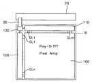
도 1을 참조하면, 일반적으로 액정패널은 칼라필터기판과 TFT 기판 사이에 액정을 봉입한 구조를 가진다.Referring to FIG. 1, a liquid crystal panel generally has a structure in which a liquid crystal is enclosed between a color filter substrate and a TFT substrate.
TFT 기판(10) 위에는 표시 셀 어레이 회로(100), 신호선 구동회로(110), 게이트선 구동회로(120), 외부연결단자(130)가 형성된다. 외부연결단자(130)는 필름 케이블(30)을 통하여 외부 통합회로기판(20)과 연결된다. 외부 통합회로기판(20)은 저전력화를 위하여 저전압, 예컨대 3V 스윙폭을 가지는 클럭신호 및 반전클럭신호와 픽셀데이터, 제어신호 등을 TFT 기판(10) 상에 구현된 구동회로에 제공한다.The display
표시 셀 어레이 회로(100)는 컬럼 방향으로 연장된 m 개의 신호선들(DL1~DLm)과 로우방향으로 연장된 n 개의 게이트선들(GL1~GLn)을 포함한다.The display
신호선 구동회로(110) 및 게이트선 구동회로(120)는 외부 개시신호에 의해 외부 저전압 클럭신호에 동기된 고전압 스캔펄스신호를 차례로 발생하는 쉬프트 레지스터를 포함한다.The signal
이하 도 2 내지 도 5를 참조하여 본 발명의 일 실시예를 설명한다.Hereinafter, an embodiment of the present invention will be described with reference to FIGS. 2 to 5.
도 2를 참조하면, 본 발명에 의한 개선된 쉬프트 레지스터(300)는 복수의 스테이지들(NSRC1~NSRCk)이 종속 연결된다.2, in the improved
각 스테이지들은 제 1 입력단자(IN), 제 2 입력단자(INB), 클럭단자(CK), 반전클럭단자(CKB), 제 1 전원전압단자(VDD), 제 2 전원전압단자(VSS), 제 1 출력단자(Y), 제 2 출력단자(OUTB), 제 3 출력단자(OUT), 리세트단자(RST)를 가진다.Each stage includes a first input terminal IN, a second input terminal INB, a clock terminal CK, an inverted clock terminal CKB, a first power supply voltage terminal VDD, a second power supply voltage terminal VSS, The first output terminal Y, the second output terminal OUTB, the third output terminal OUT, and the reset terminal RST are included.
각 스테이지들(NSRC1~NSRCk)은 스테이지(NSRC(i-1))의 제 1 출력단자(Y)와 제 2 출력단자(OUTB)가 스테이지(NSRCi)의 제 1 입력단자(IN)와 제 2 입력단자(INB)에 각각 연결되고, 스테이지(NSRCi)의 제 1 출력단자(Y)와 제 2 출력단자(OUTB)가 스테이지(NSRC(i+1))의 제 1 입력단자(IN)와 제 2 입력단자(INB)에 각각 연결되는 방식으로 종속 연결된다. 첫번째 스테이지(NSRC1)의 입력단자(IN)에는 개시신호(ST)가 연결되고, 입력단자(INB)에는 인버터(INV)를 통하여 반전된 개시신호(STB)가 연결된다.Each of the stages NSRC1 to NSRCk has a first output terminal Y and a second output terminal OUTB of the stage NSRC (i-1), the first input terminal IN and the second of the stage NSRCi. The first output terminal Y and the second output terminal OUTB of the stage NSRCi are connected to the input terminal INB, respectively, and the first input terminal IN and the first output terminal IN of the stage NSRCi (i + 1). It is cascaded in such a way that it is connected to each of the two input terminals INB. The start signal ST is connected to the input terminal IN of the first stage NSRC1, and the start signal STB inverted through the inverter INV is connected to the input terminal INB.
각 스테이지의 제 3 출력단자(OUT)에서 출력되는 펄스신호가 스캔펄스신호로 제공된다.The pulse signal output from the third output terminal OUT of each stage is provided as a scan pulse signal.
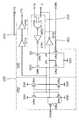
도 3을 참조하면, 본 발명에 의한 바람직한 일 실시예의 쉬프트 레지스터(300)의 각 스테이지는 입력회로(310), 레벨쉬프터(320), 제 1 출력회로(330), 제 2 출력회로(340)를 포함한다.Referring to FIG. 3, each stage of the
입력회로(310)는 제 1 입력단자(IN)와 자신의 제 1 출력단자(Y)로부터 제공되는 신호들을 조합하여 조합신호를 발생하는 노아 게이트(NOR)와 조합신호를 반전하여 제어신호(CTL)를 출력하는 인버터(INV1)를 포함한다.The
레벨쉬프터(320)는 레벨쉬프트부(322)와 래치부(324)를 포함한다.The
레벨쉬프트부(322)는 제 1 및 제 2 피모스 트랜지스터들(PM1, PM2)과 제 1 및 제 2 엔모스 트랜지스터들(NM1, NM2)를 포함한다.The
제 1 피모스 트랜지스터(PM1)는 제 1 전원전압단자(VDD)에 소오스가 연결되고, 제 1 노드(N1)에 드레인이 연결되고, 제 2 입력단자(INB)에 게이트가 결합된다. 제 1 엔모스 트랜지스터(NM1)는 제 1 노드(N1)에 드레인이 연결되고, 클럭단자(CK)에 소오스가 연결되고, 제어신호(CTL)가 게이트에 결합된다.In the first PMOS transistor PM1, a source is connected to the first power voltage terminal VDD, a drain is connected to the first node N1, and a gate is coupled to the second input terminal INB. The first NMOS transistor NM1 has a drain connected to the first node N1, a source connected to the clock terminal CK, and a control signal CTL coupled to the gate.
제 2 피모스 트랜지스터(PM2)는 제 1 전원전압단자(VDD)에 소오스가 연결되고, 제 2 노드(N2)에 드레인이 연결되고, 제 1 노드(N1)에 게이트가 결합된다. 제 2 엔모스 트랜지스터(NM2)는 제 2 노드(N2)에 드레인이 연결되고, 반전클럭단자(CKB)에 소오스가 연결되고, 제어신호(CTL)가 게이트에 결합된다.In the second PMOS transistor PM2, a source is connected to the first power voltage terminal VDD, a drain is connected to the second node N2, and a gate is coupled to the first node N1. In the second NMOS transistor NM2, a drain is connected to the second node N2, a source is connected to the inverted clock terminal CKB, and a control signal CTL is coupled to the gate.
PM1, PM2는 레벨쉬프트시 스테디 전류를 최소화하기 위하여 NM1, NM2에 비해 상대적으로 작은 사이즈, 예컨대 약 1/5 정도 사이즈를 가지도록 구성한다.PM1 and PM2 are configured to have a relatively small size, for example, about 1/5 of the size of NM1 and NM2 in order to minimize the steady current during level shift.
래치부(224)는 제 3 내지 제 4 피모스 트랜지스터들(PM3, PM4, PM5)과 제 3 및 제 4 엔모스 트랜지스터들(NM3, NM4)를 포함한다.The
제 3 피모스 트랜지스터(PM3)는 제 1 전원전압단자(VDD)에 소오스가 연결되고, 제 2 노드(N2)에 드레인이 연결되고, 제 1 노드(N1)에 게이트가 연결된다. 제 3 엔모스 트랜지스터(NM3)는 제 2 노드(N1)에 드레인이 연결되고, 제 2 전원전압단자(VSS)에 소오스가 연결되고, 제 1 노드(N1)에 게이트가 연결된다.In the third PMOS transistor PM3, a source is connected to the first power supply voltage terminal VDD, a drain is connected to the second node N2, and a gate is connected to the first node N1. In the third NMOS transistor NM3, a drain is connected to the second node N1, a source is connected to the second power supply voltage terminal VSS, and a gate is connected to the first node N1.
제 4 피모스 트랜지스터(PM4)는 제 1 전원전압단자(VDD)에 소오스가 연결되고, 제 1 노드(N1)에 드레인이 연결되고, 제 2 노드(N2)에 게이트가 연결된다. 제 4 엔모스 트랜지스터(NM4)는 제 1 노드(N2)에 드레인이 연결되고, 제 2 전원전압단자(VSS)에 소오스가 연결되고, 제 2 노드(N1)에 게이트가 연결된다.In the fourth PMOS transistor PM4, a source is connected to the first power supply voltage terminal VDD, a drain is connected to the first node N1, and a gate is connected to the second node N2. The fourth NMOS transistor NM4 has a drain connected to the first node N2, a source connected to the second power supply voltage terminal VSS, and a gate connected to the second node N1.
제 5 피모스 트랜지스터(PM5)는 제 1 전원전압단자(VDD)에 소오스가 연결되고, 제 1 노드(N1)에 드레인이 연결되고, 리세트 단자(RST)에 게이트가 연결된다.The fifth PMOS transistor PM5 has a source connected to the first power supply voltage terminal VDD, a drain connected to the first node N1, and a gate connected to the reset terminal RST.
PM3, PM4, PM5는 제 1 및 제 2 노드를 빠르게 충전시켜서 안정된 신호상태를 래치하기 위하여 NM3, NM4에 비해 상대적으로 큰 사이즈, 예컨대 약 7 내지 8배 정도 사이즈를 가지도록 구성한다.PM3, PM4, and PM5 are configured to have a relatively large size, for example, about 7 to 8 times larger than NM3 and NM4 in order to quickly charge the first and second nodes to latch a stable signal state.
제 1 출력회로(330)는 제 1 노드(N1)의 신호를 인버터(INV2)를 통하여 반전시켜서 제 1 출력단자(Y)에 출력한다.The
제 2 출력회로(340)는 인버터들(INV3, INV4)을 종속 연결한 것으로, 제 2 노드(N2)의 신호를 인버터(INV3)에서 반전시켜서 제 2 출력단자(OUTB)에 출력하고, 인버터(INV3)의 출력을 인버터(INV4)에서 반전시켜서 제 3 출력단자(OUT)에 출력한다.The
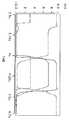
이와 같이 구성된 일실시예의 쉬프트 레지스터(300)의 동작은 도 4 및 도 5의 타이밍도를 참조하여 설명하면 다음과 같다.The operation of the
각 스테이지는 넌액티브 구간에서는 제 1 및 제 3 출력단자들(Y, OUT)의 레 벨이 로우상태, 제 2 출력단자(OUTB)의 레벨이 하이상태, 제 1 입력단자(IN)의 레벨이 로우상태, 제 2 입력단자(INB)의 레벨이 하이상태이므로, 래치부(324)에 의해 제 2 노드(N2)는 로우상태, 제 1 노드(N1)는 하이상태를 유지한다. 이때, 제어신호(CTL)는 로우상태를 유지한다. 따라서, 제 1 및 제 2 피모스 트랜지스터들(PM1, PM2) 및 제 1 및 제 2 엔모스 트랜지스터(NM1, NM2)는 모두 오프상태를 유지한다. 그러므로, 클럭단자(CK) 및 반전클럭단자(CKB)에 인가되는 클럭신호에 관계없이 출력상태는 래치부(324)에 의해 래치된 신호상태를 유지한다.In each non-active section, the levels of the first and third output terminals Y and OUT are low, the level of the second output terminal OUTB is high, and the level of the first input terminal IN is high. Since the low state and the level of the second input terminal INB are high, the
제 1 입력단자(IN)의 레벨이 하이상태로 천이하고, 제 2 입력단자(INB)의 레벨이 로우상태로 천이하게 되면, 제어신호(CTL)는 하이상태로 천이한다. 그러므로, 레벨쉬프트부(322)의 PM1, NM1, NM2는 턴온된다. 그러므로, 제 1 노드(N1)에는 턴온된 PM1과 NM1의 턴온 저항비에 의한 전압 분배에 의한 전압이 나타나게 된다.When the level of the first input terminal IN transitions to the high state and the level of the second input terminal INB transitions to the low state, the control signal CTL transitions to the high state. Therefore, PM1, NM1, and NM2 of the
도 5에 도시한 바와 같이, 클럭신호의 처음 반주기동안에는 제 1 노드(N1)는 클럭단자(CK)에 인가되는 3V에 의해 9.3V에서 약 7.2V로 레벨다운되어 출력되었다.As shown in FIG. 5, during the first half period of the clock signal, the first node N1 is outputted down from 9.3V to about 7.2V by 3V applied to the clock terminal CK.
그러나, PM2는 턴오프상태를 그대로 유지하였고, NM2만 턴온된 상태를 유지하므로, 제 2 노드(N2)는 반전클럭단자(CKB)에 인가되는 0V에 의해 0V상태를 그대로 유지하는 것으로 나타났다.However, since the PM2 maintains the turn-off state and only the NM2 is turned on, the second node N2 has been shown to maintain the 0V state by 0V applied to the inverted clock terminal CKB.
그러므로, 클럭신호의 처음 반주기 동안에는 PM1, PM4를 통하여 제 1 전원전압단자(VDD)로부터 NM1을 통하여 제 2 전원전압단자(VSS)로 제 1 스테디 전류패스만 형성된다.Therefore, during the first half period of the clock signal, only the first steady current path is formed from the first power supply voltage terminal VDD through the NM1 to the second power supply voltage terminal VSS through the PM1 and PM4.
이와 같은 상태에서 클럭신호의 위상이 반전되고, 제 2 입력단자(INB)에 인 가된 신호의 상태가 하강천이되면, PM1은 턴온되므로, 제 1 노드(N1)의 레벨이 7.2V에서 0V로 급속히 다운되어 출력되었다. 이에 PM2가 턴온되므로, PM2와 NM2의 턴온 저항비에 의한 전압이 제 2노드에 나타나게 되어 제 2 노드(N2)의 레벨은 0V에서 7.2V로 업되어 나타났다.In this state, when the phase of the clock signal is inverted and the state of the signal applied to the second input terminal INB falls, PM1 turns on, so the level of the first node N1 goes from 7.2V to 0V. The output went down quickly. Since PM2 is turned on, the voltage due to the turn-on resistance ratio of PM2 and NM2 appears in the second node, and the level of the second node N2 is raised from 0V to 7.2V.
이에, 래치부(324)에서는 상태천이된 제 1 및 제 2 노드(N1, N2)의 상태를 래치하게 된다. 제 1 출력회로(330)에서는 제 1 노드(N1)의 로우상태에 응답하여 하이상태의 제 1 출력신호를 제 1 출력단자(Y)에 출력한다. 제 2 출력회로(340)에서는 제 2 노드(N2)의 하이상태에 응답하여 버퍼링된 하이상태의 제 2 출력신호를 제 2 출력단자(OUT)에 출력하고, 반전된 로우상태의 제 3 출력신호를 제 3 출력단자(OUTB)에 출력한다.Accordingly, the
제 1 출력단자(Y)의 신호상태가 하이상태로 천이된 상태이므로 입력단자(IN)에 인가된 신호가 로우상태로 천이되더라도 제어신호(CTL)는 이전상태인 하이상태를 그대로 유지하게 된다. 그러나, 제 2 입력단자(INB)의 상태는 로우상태에서 하이상태로 천이된 상태이므로 PM1은 턴오프된 상태를 유지한다.Since the signal state of the first output terminal Y is transitioned to the high state, even when the signal applied to the input terminal IN is transitioned to the low state, the control signal CTL maintains the previous high state. However, since the state of the second input terminal INB is transitioned from the low state to the high state, PM1 remains turned off.
그러므로, 클럭신호의 다음 반주기 동안 NM1은 턴온상태를 유지하지만, PM1, PM4는 턴오프되었으므로 제 1 스테디 전류패스는 차단되고, PM2, PM3을 통하여 제 1 전원전압단자(VDD)로부터 NM2를 통하여 제 2 전원전압단자(VSS)로 제 2 스테디 전류패스만 형성된다.Therefore, NM1 remains on for the next half period of the clock signal, but since the PM1 and PM4 are turned off, the first steady current path is blocked, and the NM1 through the NM2 from the first power voltage terminal VDD through the PM2 and PM3. Only the second steady current path is formed with the second power supply voltage terminal VSS.
클럭신호의 위상이 반전되면, 제 1 노드(N1)의 레벨은 0V에서 7.2V로 업되어 출력되었고, 제 2 노드(N2)의 레벨은 7.2V에서 1.2V로 다운되어 출력되었다. 이에 출력단자(Y, OUT)의 출력신호는 하이레벨에서 로우레벨로 천이되고, 출력단자(OUTB)의 출력신호는 로우레벨에서 하이레벨로 천이된다.When the phase of the clock signal is reversed, the level of the first node N1 is increased from 0V to 7.2V, and the level of the second node N2 is output from down from 1.2V to 1.2V. Accordingly, the output signals of the output terminals Y and OUT transition from the high level to the low level, and the output signals of the output terminal OUTB transition from the low level to the high level.
그러므로, 제어신호(CTL)는 로우레벨로 천이되고, 이에 레벨쉬프트부(322)의 모든 트랜지스터들은 턴오프된다.Therefore, the control signal CTL transitions to a low level, and thus all transistors of the
따라서, 제 1 노드(N1)는 래치부(324)의 턴온된 PM4에 의해 계속 충전되므로 9V로 레벨 업되는 것으로 나타났고, 제 2 노드(N2)는 래치부(324)의 턴온된 NM3에 의해 계속 방전되므로 0V로 레벨 다운되는 것으로 나타났다.Accordingly, the first node N1 is shown to be leveled up to 9V because it is continuously charged by the turned-on PM4 of the
상술한 바와 같이, 본 발명의 일 실시예의 시프트 레지스터에서는 레벨쉬프트부(322)의 PM1과 PM2가 클럭신호의 반주기 동안 교대로 턴온된 상태를 유지하므로, 처음 반주기 동안에는 제 1 스테디 전류패스만 형성되었고, 나머지 반주기 동안에는 제 2 스테디 전류패스만 형성되었다. 또한, 제어신호의 스윙폭은 0V와 7.2V로 7.2V를 유지하는 것으로 나타났다.As described above, in the shift register according to the exemplary embodiment of the present invention, since the PM1 and PM2 of the
도 6은 본 발명에 의한 다른 실시예의 쉬프트 레지스터의 각 스테이지의 회로구성을 나타낸다. 상술한 일 실시예와 동일한 구성은 동일 부호로 처리한다.Fig. 6 shows a circuit configuration of each stage of the shift register of another embodiment according to the present invention. The same configuration as in the above-described embodiment is treated with the same reference numerals.
다른 실시예는 상술한 일 실시예와 비교하면, 레벨쉬프트부(322)의 구성에서 PM2가 제거된 레벨쉬프트부(323)를 가진다.Another embodiment has a
다른 실시예에서는 래치부(324)의 PM3가 PM2의 역할을 겸하도록 구성하였다. 즉, 일 실시예에서 레벨 쉬프트부의 PM1, PM2는 NM1, NM2에 비해 사이즈가 약 1/5 정도로 작은 반면에 래치부의 PM3, PM4는 NM3, NM4에 비해 사이즈가 약 7 내지 8배 정도로 크므로 PM2를 제거하고 PM3가 PM2를 겸용하게 구성하더라도 PM3만으로도 제 2 노드를 충분히 충전시킬 정도의 전류구동능력을 유지할 수 있다.In another embodiment, PM3 of the
상술한 다른 실시예의 동작은 상술한 일 실시예와 동일하므로 구체적인 설명은 생략한다.Operation of the other embodiment described above is the same as the embodiment described above, so a detailed description thereof will be omitted.
한편, 상술한 본 발명의 쉬프트 레지스터의 구성을 부분적으로 변경하여 비교하였다.In addition, the structure of the shift register of this invention mentioned above was changed partially and compared.
도 7 내지 도 10은 이러한 비교예로서의 쉬프트 레지스터를 나타낸다.7 to 10 show the shift register as this comparative example.
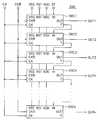
도 7을 참조하면, 마찬가지로 쉬프트 레지스터는 복수의 스테이지들(SRC1~SRCk)이 종속 연결된다.Referring to FIG. 7, in the shift register, a plurality of stages SRC1 to SRCk are cascaded.
각 스테이지들은 입력단자(IN), 클럭단자(CK), 반전클럭단자(CKB), 제 1 전원전압단자(VDD), 제 2 전원전압단자(VSS), 제 1 출력단자(Y), 제 2 출력단자(OUT), 리세트단자(RST)로 구성된다. 각 스테이지들(SRC1~SRCk)은 스테이지(SCR(i-1))의 제 1 출력단자(Y)가 스테이지(SCRi)의 입력단자(IN)에 연결되고, 스테이지(SCRi)의 제 1 출력단자(Y)가 스테이지(SCR(i+1))의 입력단자(IN)에 연결되는 방식으로 종속 연결된다. 첫 번째 스테이지(SRC1)의 입력단자(IN)에는 개시신호(ST)가 연결되도록 구성된다.Each stage includes an input terminal IN, a clock terminal CK, an inverted clock terminal CKB, a first power supply voltage terminal VDD, a second power supply voltage terminal VSS, a first output terminal Y, and a second output terminal. It consists of an output terminal OUT and a reset terminal RST. Each stage SRC1 to SRCk has a first output terminal Y of the stage SCR (i-1) connected to an input terminal IN of the stage SCRi, and a first output terminal of the stage SCRi. (Y) is cascaded in such a way that it is connected to the input terminal IN of the stage SCR (i + 1). The start signal ST is connected to the input terminal IN of the first stage SRC1.
각 스테이지의 제 2 출력단자(OUT)에서 출력되는 펄스신호가 스캔펄스신호로 제공되었다.The pulse signal output from the second output terminal OUT of each stage is provided as a scan pulse signal.
도 8을 참조하면, 비교예로서의 쉬프트 레지스터(200)의 각 스테이지는 입력회로(210), 레벨쉬프터(220), 제 1 출력회로(230), 제 2 출력회로(240)를 포함한다.Referring to FIG. 8, each stage of the
입력회로(210)는 입력단자(IN)와 자신의 제 1 출력단자(Y)로부터 제공되는 신호들을 조합하여 제 1 제어신호(C1)를 발생하는 노아 게이트(NOR)와 제 1 제어신호(C1)을 반전하여 제 2 제어신호(C2)를 출력하는 인버터(INV1)를 포함한다.The
레벨쉬프터(220)는 레벨쉬프트부(222)와 래치부(224)를 포함한다.The
레벨쉬프트부(222)는 제 1 및 제 2 피모스 트랜지스터들(PM1, PM2)과 제 1 및 제 2 엔모스 트랜지스터들(NM1, NM2)를 포함한다.The
제 1 피모스 트랜지스터(PM1)는 제 1 전원전압단자(VDD)에 소오스가 연결되고, 제 1 노드(N1)에 드레인이 연결되고, 상기 제 1 제어신호(C1)가 게이트에 결합된다. 제 1 엔모스 트랜지스터(NM1)는 제 1 노드(N1)에 드레인이 연결되고, 클럭단자(CK)에 소오스가 연결되고, 제 2 제어신호(C2)가 게이트에 결합된다.The first PMOS transistor PM1 has a source connected to the first power supply voltage terminal VDD, a drain connected to the first node N1, and the first control signal C1 coupled to the gate. In the first NMOS transistor NM1, a drain is connected to the first node N1, a source is connected to the clock terminal CK, and the second control signal C2 is coupled to the gate.
제 2 피모스 트랜지스터(PM2)는 제 1 전원전압단자(VDD)에 소오스가 연결되고, 제 2 노드(N2)에 드레인이 연결되고, 제 1 제어신호(C1)가 게이트에 결합된다. 제 2 엔모스 트랜지스터(NM2)는 제 2 노드(N2)에 드레인이 연결되고, 반전클럭단자(CKB)에 소오스가 연결되며, 제 2 제어신호(C2)가 게이트에 결합된다.The second PMOS transistor PM2 has a source connected to the first power supply voltage terminal VDD, a drain connected to the second node N2, and a first control signal C1 coupled to the gate. In the second NMOS transistor NM2, a drain is connected to the second node N2, a source is connected to the inverted clock terminal CKB, and a second control signal C2 is coupled to the gate.
래치부(224)는 제 3 내지 제 4 피모스 트랜지스터들(PM3, PM4, PM5)과 제 3 및 제 4 엔모스 트랜지스터들(NM3, NM4)를 포함한다.The
제 3 피모스 트랜지스터(PM3)는 제 1 전원전압단자(VDD)에 소오스가 연결되고, 제 2 노드(N2)에 드레인이 연결되고, 제 1 노드(N1)에 게이트가 연결된다. 제 3 엔모스 트랜지스터(NM3)는 제 2 노드(N1)에 드레인이 연결되고, 제 2 전원전압단자(VSS)에 소오스가 연결되며, 제 1 노드(N1)에 게이트가 연결된다.In the third PMOS transistor PM3, a source is connected to the first power supply voltage terminal VDD, a drain is connected to the second node N2, and a gate is connected to the first node N1. In the third NMOS transistor NM3, a drain is connected to the second node N1, a source is connected to the second power supply voltage terminal VSS, and a gate is connected to the first node N1.
제 4 피모스 트랜지스터(PM4)는 제 1 전원전압단자(VDD)에 소오스가 연결되고, 제 1 노드(N1)에 드레인이 연결되며, 제 2 노드(N2)에 게이트가 연결된다. 제 4 엔모스 트랜지스터(NM4)는 제 1 노드(N2)에 드레인이 연결되고, 제 2 전원전압단자(VSS)에 소오스가 연결되며, 제 2 노드(N1)에 게이트가 연결된다.The fourth PMOS transistor PM4 has a source connected to the first power voltage terminal VDD, a drain connected to the first node N1, and a gate connected to the second node N2. In the fourth NMOS transistor NM4, a drain is connected to the first node N2, a source is connected to the second power supply voltage terminal VSS, and a gate is connected to the second node N1.
제 5 피모스 트랜지스터(PM5)는 제 1 전원전압단자(VDD)에 소오스가 연결되고, 제 1 노드(N1)에 드레인이 연결되며, 리세트단자(RST)에 게이트가 연결된다.The fifth PMOS transistor PM5 has a source connected to the first power voltage terminal VDD, a drain connected to the first node N1, and a gate connected to the reset terminal RST.
제 1 출력회로(230)는 제 1 노드(N1)의 신호를 인버터(INV2)를 통하여 반전시켜서 제 1 출력단자(Y)로 출력한다.The
제 2 출력회로(240)는 인버터들(INV3, INV4)을 종속 연결한 것으로, 제 2 노드(N2)의 신호를 버퍼링하여 제 2 출력단자(OUT)에 출력한다.The
이와 같이 구성된 종래의 쉬프트 레지스터(200)의 동작은 도 9 및 도 10의 타이밍도를 참조하여 설명하면 다음과 같다.The operation of the
각 스테이지는 넌액티브 구간에서는 제 1 및 제 2 출력단자들(Y, OUT)의 레벨이 로우상태, 입력단자(IN)의 레벨이 로우상태이므로, 래치부(224)에 의해 제 2 노드(N2)는 로우상태, 제 1 노드(N1)는 하이상태를 유지한다. 제 1 제어신호(C1)는 하이상태, 제 2 제어신호(C2)는 로우상태를 유지한다. 따라서, 제 1 및 제 2 피모스 트랜지스터들(PM1, PM2) 및 제 1 및 제 2 엔모스 트랜지스터(NM1, NM2)는 모두 오프상태를 유지한다. 그러므로, 클럭단자(CK) 및 반전클럭단자(CKB)에 인가되는 클럭신호에 관계없이 출력상태는 래치부(224)에 의해 래치된 신호상태를 유지한다.In each stage, since the level of the first and second output terminals Y and OUT is low and the level of the input terminal IN is low in the non-active period, the second node N2 is provided by the latch unit 224. ) Is low and the first node N1 is kept high. The first control signal C1 remains high and the second control signal C2 remains low. Thus, both the first and second PMOS transistors PM1 and PM2 and the first and second NMOS transistors NM1 and NM2 remain in an off state. Therefore, the output state maintains the signal state latched by the
입력단자(IN)의 레벨이 하이상태로 천이하게 되면, 제 1 제어신호(C1)는 로 우상태로 천이하고, 제 2 제어신호(C2)는 하이상태로 천이한다. 그러므로, 레벨쉬프트부(222)의 모든 트랜지스터들은 모두 턴온된다.When the level of the input terminal IN transitions to the high state, the first control signal C1 transitions to the low state and the second control signal C2 transitions to the high state. Therefore, all the transistors of the
도 10에 도시한 바와 같이, 클럭신호의 처음 반주기 동안에는 제 1 노드(N1)는 클럭단자(CK)에 인가되는 3V에 의해 9.3V에서 약 7.2V로 레벨다운되어 나타났고, 제 2 노드(N2)는 반전클럭단자(CKB)에 인가되는 0V에 의해 0V에서 약1.2V로 레벨업되어 나타났다.As shown in FIG. 10, during the first half period of the clock signal, the first node N1 appears to be leveled down from about 9.3 V to about 7.2 V by 3 V applied to the clock terminal CK, and the second node N2. ) Is raised from 0V to about 1.2V by 0V applied to the inverted clock terminal (CKB).
그러므로, PM1, PM4를 통하여 제 1 전원전압단자(VDD)로부터 NM1을 통하여 제 2 전원전압단자(VSS)로 제 1 스테디 전류패스가 형성되고, PM2를 통하여 제 1 전원전압단자(VDD)로부터 NM2를 통하여 제 2 전원전압단자(VSS)로 제 2 스테디 전류패스가 형성된다.Therefore, a first steady current path is formed from the first power supply voltage terminal VDD through the NM1 to the second power supply voltage terminal VSS through the PM1 and PM4, and from the first power supply voltage terminal VDD to the NM2 through the PM2. A second steady current path is formed through the second power supply voltage terminal VSS.
이와 같은 상태에서 클럭신호의 위상이 반전되었을때, 도 10에 도시된 바와 같이, 제 1 노드(N1)의 레벨이 7.2V에서 1.2V로 다운되어 나타났고, 제 2 노드(N2)의 레벨은 1.2V에서 7.2V로 업되어 나타났다.In this state, when the phase of the clock signal is reversed, as shown in FIG. 10, the level of the first node N1 is lowered from 7.2V to 1.2V, and the level of the second node N2 is shown. It appeared to be up from 7.2V to 7.2V.
이에, 래치부(224)에서는 상태천이된 제 1 및 제 2 노드(N1, N2)의 상태를 래치하게 된다. 제 1 출력회로(230)에서는 제 1 노드(N1)의 로우상태에 응답하여 하이상태의 제 1 출력신호를 제 1 출력단자(Y)에 출력한다. 제 2 출력회로에서는 제 2 노드(N2)의 하이상태에 응답하여 버퍼링된 하이상태의 제 2 출력신호를 제 2 출력단자(OUT)에 출력한다.Accordingly, the
제 1 출력단자(Y)의 신호상태가 하이상태로 천이된 상태이므로 입력단자(IN)에 인가된 신호가 로우상태로 천이되더라도 제 1 및 제 2 제어신호(C1, C2)는 이전 상태를 그대로 유지한다.Since the signal state of the first output terminal Y is transitioned to the high state, even if the signal applied to the input terminal IN is transitioned to the low state, the first and second control signals C1 and C2 remain as they were. Keep it.
그러므로, 클럭신호의 다음 반주기 동안 PM1을 통하여 제 1 전원전압단자(VDD)로부터 NM1을 통하여 제 2 전원전압단자(VSS)로 제 1 스테디 전류패스가 그대로 유지되고, PM2, PM3을 통하여 제 1 전원전압단자(VDD)로부터 NM2를 통하여 제 2 전원전압단자(VSS)로 제 2 스테디 전류패스가 그대로 유지된다.Therefore, during the next half period of the clock signal, the first steady current path is maintained from the first power supply voltage terminal VDD through the NM1 to the second power supply voltage terminal VSS through the NM1, and the first power supply through the PM2 and PM3. The second steady current path is maintained from the voltage terminal VDD to the second power supply voltage terminal VSS through the NM2.
클럭신호의 위상이 반전되면, 제 1 노드(N1)의 레벨은 1.2V에서 7.2V로 업되어 출력되었고, 제 2 노드(N2)의 레벨은 7.2V에서 1.2V로 다운되어 출력되었다. 이에 출력단자(Y, OUT)의출력신호는 하이레벨에서 로우레벨로 천이되었다.When the phase of the clock signal is inverted, the level of the first node N1 is outputted from 1.2V to 7.2V, and the level of the second node N2 is outputted from 7.2V to 1.2V. As a result, the output signals of the output terminals Y and OUT have transitioned from the high level to the low level.
그러므로, 제 1 및 제 2 제어신호(C1, C2)는 모두 로우레벨로 천이되고, 이에 레벨쉬프트부(222)의 모든 트랜지스터들은 턴오프된다.Therefore, the first and second control signals C1 and C2 both transition to a low level, and thus all transistors of the
따라서, 제 1 노드(N1)는 래치부(224)의 PM4의 턴온상태에 의해 계속 충전되었으므로 9V로 레벨 업되어 출력되었고, 제 2 노드(N2)는 NM3의 턴온상태에 의해 계속 방전되었으므로 0V로 레벨 다운되어 출력되었다.Therefore, since the first node N1 is continuously charged by the turn-on state of the PM4 of the
상술한 바와 같이, 비교예와 같은 구성을 갖는 시프트 레지스터에서는 레벨쉬프트부(222)의 모든 트랜지스터들이 클럭신호의 1주기동안 지속적으로 턴온된 상태를 유지한다.As described above, in the shift register having the same configuration as that of the comparative example, all the transistors of the
즉, 도 10에 도시된 바와 같이, 스테디 전류에 의하여 클럭신호의 1주기 동안 지속적으로 전력이 소모되었다. 이에 반해, 상술한 본 발명의 일 실시예 및 다른 실시예에서는 제1 및 제2 스테디 전류패스가 교호적으로 턴온 또는 턴오프 상태를 유지한다.That is, as shown in FIG. 10, power is continuously consumed for one period of the clock signal by the steady current. In contrast, in the above-described embodiments of the present invention and the other embodiments, the first and second steady current paths alternately maintain on or off.
그러므로, 도 5에 도시된 바와 같이, 클럭신호의 1주기 동안 제 1 및 제 2 스테디 전류패스가 모두 형성된 비교예의 쉬프트 레지스터에 비하여 본 발명의 쉬프트 레지스터에서의 전력소모가 약 1/2로 감소되는 것으로 나타났다.Therefore, as shown in FIG. 5, the power consumption of the shift register of the present invention is reduced by about 1/2 compared to the shift register of the comparative example in which both the first and second steady current paths are formed during one period of the clock signal. Appeared.
또한, 제어신호의 스윙폭이 비교예의 구성의 쉬프트 레지스터에서는 도 10에 도시된 바와 같이 1.2V와 7.2V의 6V의 차이를 나타냈지만, 본 발명의 실시예들에서는 0V와 7.2V의 7.2V의 차이로 커졌으므로 레벨 쉬프트된 펄스신호의 신호 마진이 약 20%정도 향상되는 것으로 나타났다.In addition, although the swing width of the control signal shows a difference of 6V of 1.2V and 7.2V in the shift register of the configuration of the comparative example, in the embodiments of the present invention, 7.2V of 0V and 7.2V is shown. As the difference is increased, the signal margin of the level shifted pulse signal is improved by about 20%.
또한, 본 발명의 쉬프트 레지스터의 다른 실시예는 비교예의 구성을 갖는 쉬프트 레지스터에 비하여 트랜지스터의 숫자를 하나 줄일 수 있으므로 각 스테이지의 레이아웃 설계를 용이하게 하고 설계 면적을 줄일 수 있는 잇점이 있었다.Further, another embodiment of the shift register of the present invention has the advantage that the number of transistors can be reduced by one compared with the shift register having the configuration of the comparative example, thereby facilitating the layout design of each stage and reducing the design area.
상술한 바와 같이, 본 발명에서는 레벨 쉬프트부의 회로개선에 의해 각 스테이지에서 스테디 전류를 대략 1/2로 줄임으로써 전체 쉬프트 레지스터의 전력소모를 도 11에 도시한 바와 같이 2.75mW에서 2.05mW로 비교예의 쉬프트 레지스터에 비하여 약 30%정도 줄일 수 있다.As described above, in the present invention, the power consumption of the entire shift register is reduced from 2.75 mW to 2.05 mW as shown in FIG. It can be reduced by about 30% compared to the shift register.
상기에서는 본 발명의 바람직한 실시예들을 참조하여 설명하였지만, 해당 기술 분야에서 통상의 지식을 가진 자라면 하기의 특허청구의 범위에 기재된 본 발명의 사상 및 영역으로부터 벗어나지 않는 범위 내에서 본 발명을 다양하게 수정 및 변경시킬 수 있음을 이해할 수 있을 것이다.Although the above has been described with reference to the preferred embodiments of the present invention, those skilled in the art to which the present invention pertains without departing from the spirit and scope of the invention as set forth in the claims below It will be appreciated that modifications and variations can be made.
Claims (20)
Translated fromKoreanPriority Applications (4)
| Application Number | Priority Date | Filing Date | Title |
|---|---|---|---|
| KR1020010063800AKR100753365B1 (en) | 2001-10-16 | 2001-10-16 | Shift register and liquid crystal display device having same |
| TW090128018ATW533400B (en) | 2001-10-16 | 2001-11-12 | Shift register and liquid crystal display having the same |
| PCT/KR2002/000519WO2003034438A1 (en) | 2001-10-16 | 2002-03-26 | Shift resister and liquid crystal display having the same |
| US10/489,589US20040239608A1 (en) | 2001-10-16 | 2002-03-26 | Shift register and liquid crystal display having the same |
Applications Claiming Priority (1)
| Application Number | Priority Date | Filing Date | Title |
|---|---|---|---|
| KR1020010063800AKR100753365B1 (en) | 2001-10-16 | 2001-10-16 | Shift register and liquid crystal display device having same |
Publications (2)
| Publication Number | Publication Date |
|---|---|
| KR20030032199A KR20030032199A (en) | 2003-04-26 |
| KR100753365B1true KR100753365B1 (en) | 2007-08-30 |
Family
ID=19715174
Family Applications (1)
| Application Number | Title | Priority Date | Filing Date |
|---|---|---|---|
| KR1020010063800AExpired - Fee RelatedKR100753365B1 (en) | 2001-10-16 | 2001-10-16 | Shift register and liquid crystal display device having same |
Country Status (4)
| Country | Link |
|---|---|
| US (1) | US20040239608A1 (en) |
| KR (1) | KR100753365B1 (en) |
| TW (1) | TW533400B (en) |
| WO (1) | WO2003034438A1 (en) |
Families Citing this family (35)
| Publication number | Priority date | Publication date | Assignee | Title |
|---|---|---|---|---|
| KR100574363B1 (en)* | 2002-12-04 | 2006-04-27 | 엘지.필립스 엘시디 주식회사 | Shift Register with Level Shifter |
| JP4339103B2 (en) | 2002-12-25 | 2009-10-07 | 株式会社半導体エネルギー研究所 | Semiconductor device and display device |
| KR100913303B1 (en)* | 2003-05-06 | 2009-08-26 | 삼성전자주식회사 | LCD Display |
| KR101012972B1 (en)* | 2003-12-30 | 2011-02-10 | 엘지디스플레이 주식회사 | Active matrix display |
| KR101028947B1 (en)* | 2004-05-31 | 2011-04-12 | 엘지디스플레이 주식회사 | Shift register circuit |
| KR101080352B1 (en) | 2004-07-26 | 2011-11-04 | 삼성전자주식회사 | Display device |
| KR101127813B1 (en)* | 2004-12-29 | 2012-03-26 | 엘지디스플레이 주식회사 | Shift register and liquid crystal display using the same |
| KR101082909B1 (en)* | 2005-02-05 | 2011-11-11 | 삼성전자주식회사 | Gate driving method and gate driver and display device having the same |
| KR101107714B1 (en)* | 2005-04-22 | 2012-01-25 | 엘지디스플레이 주식회사 | Shift register and its driving method |
| US9153341B2 (en) | 2005-10-18 | 2015-10-06 | Semiconductor Energy Laboratory Co., Ltd. | Shift register, semiconductor device, display device, and electronic device |
| US7663592B2 (en)* | 2005-10-19 | 2010-02-16 | Tpo Displays Corp. | Systems involving signal driving circuits for driving displays |
| US7430268B2 (en)* | 2006-01-05 | 2008-09-30 | Au Optronics Corporation | Dynamic shift register with built-in disable circuit |
| KR101319356B1 (en)* | 2006-06-09 | 2013-10-16 | 엘지디스플레이 주식회사 | A shift register of a liquid crystal display device and a method for driving the same |
| KR100796125B1 (en)* | 2006-06-09 | 2008-01-21 | 삼성에스디아이 주식회사 | Shift register and data driving circuit and organic light emitting display device using the same |
| KR101296624B1 (en)* | 2006-06-26 | 2013-08-14 | 엘지디스플레이 주식회사 | Driving circuit for liquid crystal display device and method for driving the same |
| CN101154360B (en)* | 2006-09-27 | 2011-07-13 | 奇美电子股份有限公司 | Image display system and method for driving display component |
| JP2008158226A (en)* | 2006-12-22 | 2008-07-10 | Toshiba Corp | Output circuit and liquid crystal display device |
| KR101393635B1 (en) | 2007-06-04 | 2014-05-09 | 삼성디스플레이 주식회사 | Driving apparatus for display device and display device including the same |
| BRPI1013283A2 (en)* | 2009-06-15 | 2019-04-09 | Sharp Kk | shift log and display device |
| WO2011108678A1 (en) | 2010-03-02 | 2011-09-09 | Semiconductor Energy Laboratory Co., Ltd. | Pulse signal output circuit and shift register |
| CN102654982B (en)* | 2011-05-16 | 2013-12-04 | 京东方科技集团股份有限公司 | Shift register unit circuit, shift register, array substrate and liquid crystal display |
| KR101977247B1 (en)* | 2012-08-06 | 2019-05-13 | 엘지디스플레이 주식회사 | Shift register and display device using the same |
| CN103943054B (en) | 2014-01-27 | 2016-07-13 | 上海中航光电子有限公司 | Gate drive circuit, TFT array substrate, display panel and display device |
| CN104299554B (en)* | 2014-08-22 | 2017-07-18 | 京东方科技集团股份有限公司 | Shift register, array base palte and display device |
| CN104282282B (en)* | 2014-10-20 | 2018-01-05 | 京东方科技集团股份有限公司 | Shift register, driving method, gate driving circuit and display device |
| CN106683634B (en)* | 2017-03-30 | 2019-01-22 | 京东方科技集团股份有限公司 | Shift register, GOA circuit and driving method thereof, and display device |
| CN107610737B (en)* | 2017-10-26 | 2023-07-21 | 京东方科技集团股份有限公司 | Shift register unit, driving method thereof, gate driving circuit and display device |
| CN108806583B (en) | 2018-07-05 | 2020-12-01 | 京东方科技集团股份有限公司 | Shift register unit, driving method, shift register and display device |
| CN109327205B (en)* | 2018-08-23 | 2022-08-05 | 思瑞浦微电子科技(苏州)股份有限公司 | Boost clock generating circuit |
| CN109377948B (en)* | 2018-12-25 | 2020-06-05 | 合肥京东方显示技术有限公司 | Shift register and driving method thereof, grid driving circuit and display device |
| EP3951764B1 (en)* | 2019-04-02 | 2025-06-25 | BOE Technology Group Co., Ltd. | Shift register unit and driving method therefor, gate driving circuit, and display apparatus |
| CN110349536B (en)* | 2019-04-08 | 2021-02-23 | 深圳市华星光电半导体显示技术有限公司 | GOA circuit and display panel |
| CN110070828B (en)* | 2019-04-08 | 2021-02-26 | 深圳市华星光电半导体显示技术有限公司 | GOA circuit and display panel |
| CN111243649B (en)* | 2020-01-22 | 2022-04-26 | 京东方科技集团股份有限公司 | Shift register unit, display panel |
| TWI744096B (en)* | 2020-11-18 | 2021-10-21 | 友達光電股份有限公司 | Gate of array driving circuit |
Citations (4)
| Publication number | Priority date | Publication date | Assignee | Title |
|---|---|---|---|---|
| JPH06318055A (en)* | 1992-12-02 | 1994-11-15 | Seiko Epson Corp | Level shift circuit and high voltage drive circuit using the same |
| JPH09244585A (en)* | 1996-03-04 | 1997-09-19 | Toppan Printing Co Ltd | Level shifter circuit with latch function |
| JPH1065516A (en)* | 1996-08-22 | 1998-03-06 | Hitachi Ltd | Driver IC and electronic device using the same |
| JPH11150452A (en)* | 1997-11-17 | 1999-06-02 | Toshiba Microelectronics Corp | Level conversion circuit and liquid crystal display device |
Family Cites Families (9)
| Publication number | Priority date | Publication date | Assignee | Title |
|---|---|---|---|---|
| US472021A (en)* | 1892-04-05 | Stretcher for the paper or canvas of pictures | ||
| JPH06317807A (en)* | 1993-05-06 | 1994-11-15 | Sharp Corp | Matrix display device and its driving method |
| US5735083A (en)* | 1995-04-21 | 1998-04-07 | Brown; Glen J. | Braided airbeam structure |
| JP3359844B2 (en)* | 1996-07-22 | 2002-12-24 | シャープ株式会社 | Matrix type image display device |
| US5677023A (en)* | 1996-10-10 | 1997-10-14 | Brown; Glen J. | Reinforced fabric inflatable tube |
| JPH11176186A (en)* | 1997-12-11 | 1999-07-02 | Hitachi Ltd | Bidirectional shift register |
| US6580411B1 (en)* | 1998-04-28 | 2003-06-17 | Sharp Kabushiki Kaisha | Latch circuit, shift register circuit and image display device operated with a low consumption of power |
| TW461180B (en)* | 1998-12-21 | 2001-10-21 | Sony Corp | Digital/analog converter circuit, level shift circuit, shift register utilizing level shift circuit, sampling latch circuit, latch circuit and liquid crystal display device incorporating the same |
| GB9926070D0 (en)* | 1999-11-03 | 2000-01-12 | Sgs Thomson Microelectronics | Complementary logic circuit |
- 2001
- 2001-10-16KRKR1020010063800Apatent/KR100753365B1/ennot_activeExpired - Fee Related
- 2001-11-12TWTW090128018Apatent/TW533400B/ennot_activeIP Right Cessation
- 2002
- 2002-03-26USUS10/489,589patent/US20040239608A1/ennot_activeAbandoned
- 2002-03-26WOPCT/KR2002/000519patent/WO2003034438A1/ennot_activeCeased
Patent Citations (4)
| Publication number | Priority date | Publication date | Assignee | Title |
|---|---|---|---|---|
| JPH06318055A (en)* | 1992-12-02 | 1994-11-15 | Seiko Epson Corp | Level shift circuit and high voltage drive circuit using the same |
| JPH09244585A (en)* | 1996-03-04 | 1997-09-19 | Toppan Printing Co Ltd | Level shifter circuit with latch function |
| JPH1065516A (en)* | 1996-08-22 | 1998-03-06 | Hitachi Ltd | Driver IC and electronic device using the same |
| JPH11150452A (en)* | 1997-11-17 | 1999-06-02 | Toshiba Microelectronics Corp | Level conversion circuit and liquid crystal display device |
Also Published As
| Publication number | Publication date |
|---|---|
| TW533400B (en) | 2003-05-21 |
| WO2003034438A1 (en) | 2003-04-24 |
| KR20030032199A (en) | 2003-04-26 |
| US20040239608A1 (en) | 2004-12-02 |
Similar Documents
| Publication | Publication Date | Title |
|---|---|---|
| KR100753365B1 (en) | Shift register and liquid crystal display device having same | |
| US7733321B2 (en) | Shift register and display device using same | |
| KR100381064B1 (en) | Shift register and image display device | |
| US6670944B1 (en) | Shift register circuit, driving circuit for an electrooptical device, electrooptical device, and electronic apparatus | |
| US6335721B1 (en) | LCD source driver | |
| KR100832252B1 (en) | Pulse output circuit, shift register and display device | |
| KR100793507B1 (en) | Bidirectional shift register | |
| US7406146B2 (en) | Shift register circuit | |
| CN104992662B (en) | GOA unit and its driving method, GOA circuits, display device | |
| JP3588033B2 (en) | Shift register and image display device having the same | |
| JP3588020B2 (en) | Shift register and image display device | |
| US6275210B1 (en) | Liquid crystal display device and driver circuit thereof | |
| JP2008140522A (en) | Shift register circuit, image display device including the same, and voltage signal generation circuit | |
| CN100483556C (en) | Level shifter and display device using it | |
| US7920668B2 (en) | Systems for displaying images by utilizing vertical shift register circuit to generate non-overlapped output signals | |
| JP3705985B2 (en) | Shift register and image display device using the same | |
| JP4016163B2 (en) | Liquid crystal display device and data line driving circuit thereof | |
| CN111276177B (en) | Shift register and driving method thereof, gate drive circuit and display device | |
| JP3742088B2 (en) | Shift register and image display device | |
| JPH11134893A (en) | Shift register and driving circuit of matrix-type liquid crystal display device using the shift register | |
| JP5246726B2 (en) | Shift register circuit and display device | |
| US7623110B2 (en) | Systems for displaying images by utilizing horizontal shift register circuit for generating overlapped output signals | |
| CN111161689B (en) | GOA circuit and display panel thereof | |
| JP3270299B2 (en) | Synchronous circuit driving method, synchronous signal control circuit, and image display device using the same | |
| JP3767752B2 (en) | Image display device |
Legal Events
| Date | Code | Title | Description |
|---|---|---|---|
| PA0109 | Patent application | St.27 status event code:A-0-1-A10-A12-nap-PA0109 | |
| PN2301 | Change of applicant | St.27 status event code:A-3-3-R10-R13-asn-PN2301 St.27 status event code:A-3-3-R10-R11-asn-PN2301 | |
| R18-X000 | Changes to party contact information recorded | St.27 status event code:A-3-3-R10-R18-oth-X000 | |
| R18-X000 | Changes to party contact information recorded | St.27 status event code:A-3-3-R10-R18-oth-X000 | |
| PG1501 | Laying open of application | St.27 status event code:A-1-1-Q10-Q12-nap-PG1501 | |
| R18-X000 | Changes to party contact information recorded | St.27 status event code:A-3-3-R10-R18-oth-X000 | |
| PN2301 | Change of applicant | St.27 status event code:A-3-3-R10-R13-asn-PN2301 St.27 status event code:A-3-3-R10-R11-asn-PN2301 | |
| PN2301 | Change of applicant | St.27 status event code:A-3-3-R10-R13-asn-PN2301 St.27 status event code:A-3-3-R10-R11-asn-PN2301 | |
| A201 | Request for examination | ||
| PA0201 | Request for examination | St.27 status event code:A-1-2-D10-D11-exm-PA0201 | |
| D13-X000 | Search requested | St.27 status event code:A-1-2-D10-D13-srh-X000 | |
| D14-X000 | Search report completed | St.27 status event code:A-1-2-D10-D14-srh-X000 | |
| E701 | Decision to grant or registration of patent right | ||
| PE0701 | Decision of registration | St.27 status event code:A-1-2-D10-D22-exm-PE0701 | |
| GRNT | Written decision to grant | ||
| PR0701 | Registration of establishment | St.27 status event code:A-2-4-F10-F11-exm-PR0701 | |
| PR1002 | Payment of registration fee | St.27 status event code:A-2-2-U10-U11-oth-PR1002 Fee payment year number:1 | |
| PG1601 | Publication of registration | St.27 status event code:A-4-4-Q10-Q13-nap-PG1601 | |
| PR1001 | Payment of annual fee | St.27 status event code:A-4-4-U10-U11-oth-PR1001 Fee payment year number:4 | |
| PR1001 | Payment of annual fee | St.27 status event code:A-4-4-U10-U11-oth-PR1001 Fee payment year number:5 | |
| R18-X000 | Changes to party contact information recorded | St.27 status event code:A-5-5-R10-R18-oth-X000 | |
| FPAY | Annual fee payment | Payment date:20120814 Year of fee payment:6 | |
| PR1001 | Payment of annual fee | St.27 status event code:A-4-4-U10-U11-oth-PR1001 Fee payment year number:6 | |
| PN2301 | Change of applicant | St.27 status event code:A-5-5-R10-R11-asn-PN2301 | |
| PN2301 | Change of applicant | St.27 status event code:A-5-5-R10-R14-asn-PN2301 | |
| FPAY | Annual fee payment | Payment date:20130731 Year of fee payment:7 | |
| PR1001 | Payment of annual fee | St.27 status event code:A-4-4-U10-U11-oth-PR1001 Fee payment year number:7 | |
| PR1001 | Payment of annual fee | St.27 status event code:A-4-4-U10-U11-oth-PR1001 Fee payment year number:8 | |
| PR1001 | Payment of annual fee | St.27 status event code:A-4-4-U10-U11-oth-PR1001 Fee payment year number:9 | |
| R18-X000 | Changes to party contact information recorded | St.27 status event code:A-5-5-R10-R18-oth-X000 | |
| L13-X000 | Limitation or reissue of ip right requested | St.27 status event code:A-2-3-L10-L13-lim-X000 | |
| U15-X000 | Partial renewal or maintenance fee paid modifying the ip right scope | St.27 status event code:A-4-4-U10-U15-oth-X000 | |
| FPAY | Annual fee payment | Payment date:20160801 Year of fee payment:10 | |
| PR1001 | Payment of annual fee | St.27 status event code:A-4-4-U10-U11-oth-PR1001 Fee payment year number:10 | |
| LAPS | Lapse due to unpaid annual fee | ||
| PC1903 | Unpaid annual fee | St.27 status event code:A-4-4-U10-U13-oth-PC1903 Not in force date:20170824 Payment event data comment text:Termination Category : DEFAULT_OF_REGISTRATION_FEE | |
| PC1903 | Unpaid annual fee | St.27 status event code:N-4-6-H10-H13-oth-PC1903 Ip right cessation event data comment text:Termination Category : DEFAULT_OF_REGISTRATION_FEE Not in force date:20170824 |