KR100752215B1 - Transverse electric field type liquid crystal display device and manufacturing method thereof - Google Patents
Transverse electric field type liquid crystal display device and manufacturing method thereofDownload PDFInfo
- Publication number
- KR100752215B1 KR100752215B1KR1020030087560AKR20030087560AKR100752215B1KR 100752215 B1KR100752215 B1KR 100752215B1KR 1020030087560 AKR1020030087560 AKR 1020030087560AKR 20030087560 AKR20030087560 AKR 20030087560AKR 100752215 B1KR100752215 B1KR 100752215B1
- Authority
- KR
- South Korea
- Prior art keywords
- color filter
- substrate
- filter layer
- pixel
- pixel region
- Prior art date
- Legal status (The legal status is an assumption and is not a legal conclusion. Google has not performed a legal analysis and makes no representation as to the accuracy of the status listed.)
- Expired - Fee Related
Links
Images


Classifications
- G—PHYSICS
- G02—OPTICS
- G02F—OPTICAL DEVICES OR ARRANGEMENTS FOR THE CONTROL OF LIGHT BY MODIFICATION OF THE OPTICAL PROPERTIES OF THE MEDIA OF THE ELEMENTS INVOLVED THEREIN; NON-LINEAR OPTICS; FREQUENCY-CHANGING OF LIGHT; OPTICAL LOGIC ELEMENTS; OPTICAL ANALOGUE/DIGITAL CONVERTERS
- G02F1/00—Devices or arrangements for the control of the intensity, colour, phase, polarisation or direction of light arriving from an independent light source, e.g. switching, gating or modulating; Non-linear optics
- G02F1/01—Devices or arrangements for the control of the intensity, colour, phase, polarisation or direction of light arriving from an independent light source, e.g. switching, gating or modulating; Non-linear optics for the control of the intensity, phase, polarisation or colour
- G02F1/13—Devices or arrangements for the control of the intensity, colour, phase, polarisation or direction of light arriving from an independent light source, e.g. switching, gating or modulating; Non-linear optics for the control of the intensity, phase, polarisation or colour based on liquid crystals, e.g. single liquid crystal display cells
- G02F1/133—Constructional arrangements; Operation of liquid crystal cells; Circuit arrangements
- G02F1/1333—Constructional arrangements; Manufacturing methods
- G02F1/1343—Electrodes
- G—PHYSICS
- G02—OPTICS
- G02F—OPTICAL DEVICES OR ARRANGEMENTS FOR THE CONTROL OF LIGHT BY MODIFICATION OF THE OPTICAL PROPERTIES OF THE MEDIA OF THE ELEMENTS INVOLVED THEREIN; NON-LINEAR OPTICS; FREQUENCY-CHANGING OF LIGHT; OPTICAL LOGIC ELEMENTS; OPTICAL ANALOGUE/DIGITAL CONVERTERS
- G02F1/00—Devices or arrangements for the control of the intensity, colour, phase, polarisation or direction of light arriving from an independent light source, e.g. switching, gating or modulating; Non-linear optics
- G02F1/01—Devices or arrangements for the control of the intensity, colour, phase, polarisation or direction of light arriving from an independent light source, e.g. switching, gating or modulating; Non-linear optics for the control of the intensity, phase, polarisation or colour
- G02F1/13—Devices or arrangements for the control of the intensity, colour, phase, polarisation or direction of light arriving from an independent light source, e.g. switching, gating or modulating; Non-linear optics for the control of the intensity, phase, polarisation or colour based on liquid crystals, e.g. single liquid crystal display cells
- G02F1/133—Constructional arrangements; Operation of liquid crystal cells; Circuit arrangements
- G02F1/1333—Constructional arrangements; Manufacturing methods
- G02F1/1335—Structural association of cells with optical devices, e.g. polarisers or reflectors
- G02F1/133509—Filters, e.g. light shielding masks
- G02F1/133514—Colour filters
- G—PHYSICS
- G02—OPTICS
- G02F—OPTICAL DEVICES OR ARRANGEMENTS FOR THE CONTROL OF LIGHT BY MODIFICATION OF THE OPTICAL PROPERTIES OF THE MEDIA OF THE ELEMENTS INVOLVED THEREIN; NON-LINEAR OPTICS; FREQUENCY-CHANGING OF LIGHT; OPTICAL LOGIC ELEMENTS; OPTICAL ANALOGUE/DIGITAL CONVERTERS
- G02F2201/00—Constructional arrangements not provided for in groups G02F1/00 - G02F7/00
- G02F2201/52—RGB geometrical arrangements
Landscapes
- Physics & Mathematics (AREA)
- Nonlinear Science (AREA)
- Mathematical Physics (AREA)
- Chemical & Material Sciences (AREA)
- Crystallography & Structural Chemistry (AREA)
- General Physics & Mathematics (AREA)
- Optics & Photonics (AREA)
- Liquid Crystal (AREA)
- Optical Filters (AREA)
Abstract
Translated fromKoreanDescription
Translated fromKorean도 1은 종래의 컬러필터기판의 개략적인 구성도1 is a schematic configuration diagram of a conventional color filter substrate
도 2는 도 1의 Ⅰ~Ⅰ`의 선상에 따른 종래의 컬러필터기판의 단면도FIG. 2 is a cross-sectional view of a conventional color filter substrate taken along the line I-I ′ of FIG.
도 3a 내지 도 3c는 도 1의 Ⅰ~Ⅰ`의 선상에 따른 종래의 컬러필터기판의 공정단면도3A to 3C are cross-sectional views of a conventional color filter substrate taken along the line I-I ′ of FIG.
도 4는 본 발명의 실시예에 따른 컬러필터기판의 평면도4 is a plan view of a color filter substrate according to an embodiment of the present invention;
도 5는 도 4의 Ⅱ~Ⅱ`의 선상에 따른 컬러필터기판의 단면도FIG. 5 is a cross-sectional view of the color filter substrate along the line II-II ′ of FIG. 4; FIG.
도 6은 흰색에 대한 색 재현성을 높이기 위해 제 3 보조컬러필터층의 두께가 조절된 컬러필터기판의 단면도FIG. 6 is a cross-sectional view of a color filter substrate on which a thickness of a third auxiliary color filter layer is adjusted to increase color reproducibility on white; FIG.
도 7은 광의 파장에 따른 적색, 녹색, 청색 및 흰색에 대한 투과도를 나타낸 스펙트럼7 is a spectrum showing transmittances for red, green, blue, and white depending on the wavelength of light.
도 8a 내지 도 8e는 도 4의 Ⅱ~Ⅱ`의 선상에 따른 컬러필터기판의 공정단면도8A through 8E are cross-sectional views of the color filter substrate along the line II-II ′ of FIG. 4.
도 9는 본 발명의 실시예에 따른 횡전계방식 액정표시장치의 제 1 기판의 4개의 화소영역에 대한 개략적인 구성도9 is a schematic configuration diagram of four pixel areas of a first substrate of a transverse electric field type liquid crystal display device according to an exemplary embodiment of the present invention.
도 10은 도 9의 제 1 기판의 각 화소영역에 대응하는 제 2 기판의 각 컬러필 터층 및 각 보조컬러필터층에 대한 개략적인 구성도FIG. 10 is a schematic configuration diagram of each color filter layer and each auxiliary color filter layer of a second substrate corresponding to each pixel region of the first substrate of FIG. 9;
도 11은 도 9 및 도 10의 Ⅲ~Ⅲ`의 선상에 따른 액정표시장치의 단면도FIG. 11 is a cross-sectional view of the liquid crystal display device taken along line III-III ′ of FIGS. 9 and 10.
도 12는 공통전극 및 제 4 화소영역에 형성된 각 보조컬러필터층간의 대응관계를 나타낸 공통전극 및 보조컬러필터층의 평면도12 is a plan view of a common electrode and an auxiliary color filter layer showing a correspondence relationship between each of the auxiliary color filter layers formed in the common electrode and the fourth pixel region;
도 13a 및 도 13c는 본 발명의 실시예에 따른 액정표시장치의 공정단면도13A and 13C are cross-sectional views of a liquid crystal display according to an exemplary embodiment of the present invention.
*도면의 주요부에 대한 부호 설명* Explanation of symbols on the main parts of the drawings
101a : 제 1 컬러필터층 101b : 제 2 컬러필터층101a: first
101c : 제 3 컬러필터층 111a : 제 1 보조컬러필터층101c: third
111b : 제 2 보조컬러필터층 111c : 제 3 보조컬러필터층111b: second auxiliary
BM : 블랙매트릭스층BM: Black Matrix Layer
본 발명은 액정표시장치에 관한 것으로, 특히 흰색에 대한 색 재현성을 높일 수 있으며, 공정수를 줄일 수 있는 액정표시장치 및 이의 제조방법에 관한 것이다.BACKGROUND OF THE
정보화 사회가 발전함에 따라 표시장치에 대한 요구도 다양한 형태로 점증하고 있으며, 이에 부응하여 근래에는 LCD(Liquid Crystal Display), PDP(Plasma Display Panel), ELD(Electro Luminescent Display), VFD(Vacuum Fluorescent Display)등 여러 가지 평판 표시 장치가 연구되어 왔고, 일부는 이미 여러 장비에서 표시장치로 활용되고 있다.As the information society develops, the demand for display devices is increasing in various forms.In recent years, liquid crystal display (LCD), plasma display panel (PDP), electro luminescent display (ELD), and vacuum fluorescent display (VFD) have been developed. Various flat panel display devices have been studied, and some of them are already used as display devices in various devices.
그 중에, 현재 화질이 우수하고 경량, 박형, 저소비 전력의 장점으로 인하여 이동형 화상 표시장치의 용도로 CRT(Cathode Ray Tube)를 대체하면서 LCD가 가장 많이 사용되고 있으며, 노트북 컴퓨터의 모니터와 같은 이동형의 용도 이외에도 방송신호를 수신하여 디스플레이하는 텔레비전, 및 컴퓨터의 모니터 등으로 다양하게 개발되고 있다.Among them, LCD is the most widely used as a substitute for CRT (Cathode Ray Tube) for the use of mobile image display device because of the excellent image quality, light weight, thinness, and low power consumption, and mobile type such as monitor of notebook computer. In addition, it is being developed in various ways, such as a television for receiving and displaying broadcast signals, and a monitor of a computer.
이와 같이 액정표시장치가 여러 분야에서 화면 표시장치로서의 역할을 하기 위해 여러 가지 기술적인 발전이 이루어 졌음에도 불구하고 화면 표시장치로서 화상의 품질을 높이는 작업은 상기 장점과 배치되는 면이 많이 있다.As described above, although various technical advances have been made in order for the liquid crystal display device to serve as a screen display device in various fields, the task of improving the image quality as the screen display device has many advantages and disadvantages.
따라서, 액정표시장치가 일반적인 화면 표시장치로서 다양한 부분에 사용되기 위해서는 경량, 박형, 저 소비전력의 특징을 유지하면서도 고정세, 고휘도, 대면적 등 고 품위 화상을 얼마나 구현할 수 있는가에 발전의 관건이 걸려 있다고 할 수 있다.Therefore, in order to use a liquid crystal display device in various parts as a general screen display device, the key to development is how much high definition images such as high definition, high brightness, and large area can be realized while maintaining the characteristics of light weight, thinness, and low power consumption. It can be said.
이와 같은 액정표시장치는, 화상을 표시하는 액정패널과 상기 액정패널에 구동신호를 인가하기 위한 구동부로 크게 구분될 수 있으며, 상기 액정패널은 공간을 갖고 합착된 제 1, 제 2 기판과, 상기 제 1, 제 2 기판 사이에 주입된 액정층으로 구성된다.Such a liquid crystal display device may be broadly divided into a liquid crystal panel displaying an image and a driving unit for applying a driving signal to the liquid crystal panel, wherein the liquid crystal panel includes a space between the first and second substrates, and It consists of the liquid crystal layer injected between the 1st, 2nd board | substrate.
여기서, 상기 제 1 기판(TFT 어레이 기판)에는, 일정 간격을 갖고 일방향으 로 배열되는 복수개의 게이트 라인과, 상기 각 게이트 라인과 수직한 방향으로 일정한 간격으로 배열되는 복수개의 데이터 라인과, 상기 각 게이트 라인과 데이터 라인이 교차되어 정의된 각 화소 영역에 매트릭스 형태로 형성되는 복수개의 화소 전극과 상기 게이트 라인의 신호에 의해 스위칭되어 상기 데이터 라인의 신호를 상기 각 화소 전극에 전달하는 복수개의 박막 트랜지스터가 형성되어 있다.The first substrate (TFT array substrate) may include a plurality of gate lines arranged in one direction at a predetermined interval, a plurality of data lines arranged at regular intervals in a direction perpendicular to the gate lines, A plurality of thin film transistors which are switched by a plurality of pixel electrodes formed in a matrix form in each pixel region defined by crossing gate lines and data lines and signals of the gate lines to transfer the signals of the data lines to the pixel electrodes. Is formed.
그리고, 제 2 기판(컬러필터기판)에는, 상기 화소 영역을 제외한 부분의 빛을 차단하기 위한 블랙매트릭스층과, 컬러 색상을 표현하기 위한 R, G, B 컬러필터층과 화상을 구현하기 위한 공통 전극이 형성되어 있다.In addition, the second substrate (color filter substrate) includes a black matrix layer for blocking light in portions other than the pixel region, an R, G, and B color filter layers for expressing color colors, and a common electrode for implementing an image. Is formed.
이와 같은 상기 제 1, 제 2 기판은 스페이서(spacer)에 의해 일정 공간을 갖고 시일재(sealant)에 의해 합착되고 상기 두 기판 사이에 액정이 형성된다.The first and second substrates have a predetermined space by spacers and are bonded by a sealant to form a liquid crystal between the two substrates.
한편, 상기 제 1 기판과 제 2 기판의 마주보는 면에는 각각 배향막이 형성되고 상기 액정층을 배향시키기 위하여 러빙처리된다.On the other hand, an alignment layer is formed on the facing surfaces of the first substrate and the second substrate, respectively, and is rubbed to align the liquid crystal layer.
여기서, 상기 제 2 기판의 컬러필터층은, 단위픽셀이 3개의 서브픽셀로 구성될 경우, 일반적으로 R(적색), G(녹색), B(청색)의 3종류의 컬러필터층으로 이루어지는데, 최근에는 액정패널에 표시되는 화상의 휘도를 증가시키기 위하여, 상기 단위픽셀을 4개의 서브픽셀로 구성한 경우가 있다.Here, the color filter layer of the second substrate is generally composed of three types of color filter layers of R (red), G (green), and B (blue) when the unit pixel is composed of three subpixels. In some cases, in order to increase the luminance of an image displayed on the liquid crystal panel, the unit pixel may be configured by four subpixels.
즉, 상기 R, G, B 컬러필터층 이외에 투명한 흰색(W) 컬러필터층을 더 구비하여 R, G, B, W 의 4 종의 컬러필터층을 사용하고 있다.That is, a transparent white (W) color filter layer is further provided in addition to the R, G, and B color filter layers, and four color filter layers of R, G, B, and W are used.
이하 첨부된 도면을 참조하여 종래의 R, G, B, W 의 컬러필터층을 사용한 컬러필터기판을 상세히 설명하면 다음과 같다.Hereinafter, a color filter substrate using a color filter layer of conventional R, G, B, and W will be described in detail with reference to the accompanying drawings.
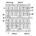
도 1은 종래의 컬러필터기판의 개략적인 구성도이고, 도 2는 도 1의 Ⅰ~Ⅰ`의 선상에 따른 종래의 컬러필터기판의 단면도이다.FIG. 1 is a schematic configuration diagram of a conventional color filter substrate, and FIG. 2 is a cross-sectional view of a conventional color filter substrate taken along lines I to I ′ of FIG. 1.
종래의 컬러필터기판은, 도 1 및 도 2에 도시된 바와 같이, 다수개의 제 1, 제 2, 제 3, 제 4 화소영역으로 반복되어 정의되는 기판(10)과, 상기 화소영역을 제외한 기판(10)의 전면에 형성되어 상기 화소영역을 제외한 부분의 빛을 차단하기 위한 블랙매트릭스층(BM)과, 상기 각 화소영역에 형성되는 제 1, 제 2, 제 3, 제 4 컬러필터층(11a, 11b, 11c, 11d)과, 상기 각 컬러필터층(11a, 11b, 11c, 11d)을 포함한 기판(10)의 전면에 형성되는 오버코트층(12)으로 구성되어 있다.In the conventional color filter substrate, as illustrated in FIGS. 1 and 2, a
여기서, 상기 제 1, 제 2, 제 3 컬러필터층(11a, 11b, 11c, 11d)은 안료가 염색된 레지스트 또는 수지를 사용하게 된다.Here, the first, second, and third
즉, 상기 제 1, 제 2, 제 3 컬러필터층(11a, 11b, 11c, 11d)은 각각 적색, 녹색, 청색의 안료가 염색된 레지스트 또는 수지를 사용하여 형성되어, 각각의 색상을 표현하게 된다.That is, the first, second, and third
그리고, 상기 제 4 컬러필터층(11d)은 아무런 염료도 염색되지 않은 투명 레지스트 및 수지를 사용하여 형성되어, 입사되는 광을 모두 통과시켜서 휘도를 증가시키는 역할을 한다.In addition, the fourth
이와 같이 구성된 종래의 컬러필터기판의 제조공정을 상세히 설명하면 다음과 같다.Referring to the manufacturing process of the conventional color filter substrate configured as described above in detail.
도 3a 내지 도 3c는 도 1의 Ⅰ~Ⅰ`의 선상에 따른 종래의 컬러필터기판의 공정단면도이다.3A to 3C are cross-sectional views of a conventional color filter substrate taken along the lines I to I 'of FIG.
먼저, 도 3a에 도시된 바와 같이, 다수개의 제 1, 제 2, 제 3, 제 4 화소영역으로 반복되어 정의되는 기판(10)을 준비하여, 상기 기판(10)에 크롬 또는 수지 등을 증착하고 포토 및 식각공정을 통해 패터닝하여, 상기 각 화소영역을 제외한 기판(10)의 전면에 블랙매트릭스층(BM) 형성한다.First, as illustrated in FIG. 3A, a
이어서, 도 3b에 도시된 바와 같이, 상기 블랙매트릭스층(BM)이 형성된 기판(10)의 전면에 적색 레지스트 또는 수지를 도포하고 포토 및 식각공정을 통해 패터닝하여, 상기 기판(10)의 제 1 화소영역에 제 1 컬러필터층(11a)을 형성한다.Subsequently, as shown in FIG. 3B, a red resist or a resin is applied to the entire surface of the
다음으로, 도 3c에 도시된 바와 같이, 상기 제 1 컬러필터층(11a)이 형성된 기판(10)의 전면에 녹색 레지스트 또는 수지를 도포하고 포토 및 식각공정을 통해 패터닝하여, 상기 기판(10)의 제 2 화소영역에 제 2 컬러필터층(11b)을 형성한다.Next, as shown in FIG. 3C, a green resist or a resin is applied to the entire surface of the
이후, 상기 제 1, 제 2 컬러필터층(11a, 11b)이 형성된 기판(10)의 전면에 청색 레지스트 또는 수지를 도포하고 포토 및 식각공정을 통해 패터닝하여, 상기 기판(10)의 제 3 화소영역에 제 3 컬러필터층(11c)을 형성한다.Thereafter, a blue resist or resin is coated on the entire surface of the
이어서, 상기 제 1, 제 2, 제 3 컬러필터층(11a, 11b, 11c)이 형성된 기판(10)에 투명 레지스트를 도포하고 포토 및 식각공정을 통해 패터닝하여, 상기 기판(10)의 제 4 영역에 제 4 컬러필터층(11d)을 형성하고, 상기 제 1, 제 2, 제 3, 제 4 컬러필터층(11d)을 포함한 기판(10)의 전면에 오버코트층(12)을 형성하여 컬러필터기판을 제조한다.Subsequently, a transparent resist is applied to the
그러나, 종래의 R, G, B, W 컬러필터층을 사용한 컬러필터기판에는 다음과 같은 문제점이 있었다.However, the color filter substrate using the conventional R, G, B, W color filter layer has the following problems.
종래의 컬러필터기판의 제조공정에서는 상기 흰색 컬러필터층을 형성하기 위하여, 상기 투명 레지스트를 도포하는 공정, 상기 투명 레지스트를 포토 및 식각하는 공정 등이 추가되어 공정시간이 늘어나고 공정수율이 감소하는 문제점이 있었다.In the conventional manufacturing process of the color filter substrate, in order to form the white color filter layer, the process of applying the transparent resist, the process of photo and etching the transparent resist is added to increase the process time and decrease the process yield there was.
또한, 흰색 컬러필터층에 의해서 표현되는 흰색과, 나머지 타 화소영역의 R, G, B 에 의해서 표현되는 흰색은 색재현성에 있어서 서로 차이가 나게 되어 전체적인 흰색에 대한 재현성이 떨어지는 문제점이 있었다.In addition, the white color represented by the white color filter layer and the white color represented by R, G, and B of the other pixel areas are different from each other in color reproducibility, thereby reducing the reproducibility of the overall white color.
본 발명은 상기와 같은 문제점을 해결하기 위하여 안출한 것으로, 제 1, 제 2, 제 3 화소영역에 각각 제 1, 제 2, 제 3 컬러필터층을 형성함과 동시에 제 4 화소영역에 상기 제 1, 제 2, 제 3 컬러필터층보다 넓이가 작은 제 1, 제 2, 제 3 보조컬러필터층을 형성하여 상기 제 4 화소영역에서는 제 1, 제 2, 제 3 보조컬러필터층에 의해서 흰색이 표현되도록 함으로써, 공정수를 줄일 수 있고 각 화소영역간의 단차를 줄일 수 있으며 흰색에 대한 색 재현성을 높일 수 있는 액정표시장치 및 이의 제조방법을 제공하는데 그 목적이 있다.The present invention has been made to solve the above problems, and the first, second, and third color filter layers are formed in the first, second, and third pixel regions, respectively, and the first in the fourth pixel region. And forming first, second and third auxiliary color filter layers having a smaller width than the second and third color filter layers so that white is represented by the first, second and third auxiliary color filter layers in the fourth pixel area. It is an object of the present invention to provide a liquid crystal display device and a method of manufacturing the same, which can reduce the number of processes, reduce the step difference between each pixel region, and improve the color reproducibility of white.
상기와 같은 목적을 달성하기 위한 본 발명에 따른 액정표시장치는, 다수개의 제 1, 제 2, 제 3, 제 4 화소영역으로 반복되어 정의되는 제 1, 제 2 기판과; 상기 각 화소영역을 제외한 제 2 기판의 전면에 형성되는 블랙매트릭스층과; 상기 각 제 1, 제 2, 제 3 화소영역에 각각 형성되는 제 1, 제 2, 제 3 컬러필터층과; 상기 제 2 기판의 각 제 4 화소영역에 형성되어 상기 제 4 화소영역에 흰색이 표현되도록 하기 위한 제 1, 제 2, 제 3 보조컬러필터층과; 상기 제 1, 제 2 기판 사이에 형성된 액정층을 포함하여 구성되는 것을 그 특징으로 한다.According to an aspect of the present invention, there is provided a liquid crystal display device including: first and second substrates repeatedly defined by a plurality of first, second, third, and fourth pixel regions; A black matrix layer formed on the entire surface of the second substrate except for the pixel areas; First, second and third color filter layers respectively formed in the first, second and third pixel regions; First, second, and third auxiliary color filter layers formed in each of the fourth pixel areas of the second substrate to express white in the fourth pixel area; The liquid crystal layer is formed between the first and second substrates.
또한, 상기와 같은 본 발명에 따른 액정표시장치의 제조방법은, 다수개의 제 1, 제 2, 제 3, 제 4 화소영역으로 반복되어 정의되는 제 1 기판 및 제 2 기판을 준비하는 단계와; 상기 각 화소영역을 제외한 상기 제 2 기판의 전면에 블랙매트릭스층을 형성하는 단계와; 상기 제 2 기판의 각 제 1 화소영역에 제 1 컬러필터층을 형성함과 동시에 상기 각 제 4 화소영역에 제 1 보조컬러필터층을 형성하는 단계와; 상기 제 2 기판의 각 제 2 화소영역에 제 2 컬러필터층을 형성함과 동시에 상기 각 제 4 화소영역에 제 2 보조컬러필터층을 형성하는 단계와; 상기 제 2 기판의 각 제 3 화소영역에 제 3 컬러필터층을 형성함과 동시에 상기 각 제 4 화소영역에 제 3 보조컬러필터층을 형성하는 단계와; 상기 제 1, 제 2 기판을 합착하고, 상기 제 1, 제 2 기판의 사이에 액정층을 형성하는 단계를 포함하여 이루어지는 것을 그 특징으로 한다.In addition, the manufacturing method of the liquid crystal display device according to the present invention as described above comprises the steps of preparing a first substrate and a second substrate that is repeatedly defined in a plurality of first, second, third, fourth pixel region; Forming a black matrix layer on an entire surface of the second substrate except for the pixel areas; Forming a first color filter layer in each of the first pixel areas of the second substrate and simultaneously forming a first auxiliary color filter layer in each of the fourth pixel areas; Forming a second color filter layer in each second pixel region of the second substrate and forming a second auxiliary color filter layer in each of the fourth pixel regions; Forming a third color filter layer in each third pixel region of the second substrate and simultaneously forming a third auxiliary color filter layer in each of the fourth pixel regions; And bonding the first and second substrates to form a liquid crystal layer between the first and second substrates.
이하 첨부된 도면을 참조하여 본 발명에 따른 액정표시장치 및 이의 제조방법을 상세히 설명하면 다음과 같다.Hereinafter, a liquid crystal display and a manufacturing method thereof according to the present invention will be described in detail with reference to the accompanying drawings.
도 4는 본 발명의 실시예에 따른 컬러필터기판의 평면도이고, 도 5는 도 4의 Ⅱ~Ⅱ`의 선상에 따른 컬러필터기판의 단면도이다.4 is a plan view of a color filter substrate according to an exemplary embodiment of the present invention, and FIG. 5 is a cross-sectional view of the color filter substrate taken along line II-II ′ of FIG. 4.
그리고, 도 6은 흰색에 대한 색 재현성을 높이기 위해 제 3 보조컬러필터층의 두께가 조절된 컬러필터기판의 단면도이고, 도 7은 광의 파장에 따른 적색, 녹색, 청색 및 흰색에 대한 투과도를 나타낸 스펙트럼이다.6 is a cross-sectional view of a color filter substrate in which the thickness of the third auxiliary color filter layer is adjusted to increase color reproducibility with respect to white, and FIG. 7 is a spectrum showing transmittances for red, green, blue, and white according to wavelengths of light. to be.
본 발명의 실시예에 따른 액정표시장치의 컬러필터기판은, 도 4및 도 5에 도시된 바와 같이, 다수개의 제 1, 제 2, 제 3, 제 4 화소영역으로 반복되어 정의되는 기판(100)과, 상기 각 화소영역을 제외한 기판(100)의 전면에 형성되어 상기 각 화소영역을 제외한 부분의 빛을 차단하기 위한 블랙매트릭스층(BM)과, 상기 각 제 1, 제 2, 제 3 화소영역에 각각 형성되는 제 1, 제 2, 제 3 컬러필터층(101a, 101b, 101c)과, 상기 각 제 4 화소영역에 형성되어 상기 제 4 화소영역에 흰색이 표현되도록 함과 동시에 상기 제 4 화소영역과 타 화소영역들과의 단차를 줄이기 위한 제 1, 제 2, 제 3 보조컬러필터층(111a, 111b, 111c)과, 상기 각 컬러필터층(101a, 101b, 101c) 및 보조컬러필터층(111a, 111b, 111c)을 포함한 기판(100)의 전면에 형성되어 상기 기판(100)을 평탄화함과 동시에 상기 제 4 화소영역에서 화이트 컬러를 구현하기 위한 오버코트층(102)으로 구성되어 있다.As shown in FIGS. 4 and 5, the color filter substrate of the liquid crystal display according to the exemplary embodiment of the present invention is a
여기서, 상기 제 4 화소영역에는 제 1, 제 2, 제 3 보조컬러필터층(111a, 111b, 111c)이 함께 형성되어 있으며, 상기 제 1, 제 2, 제 3 보조컬러필터층(111a, 111b, 111c)은 상기 제 1, 제 2, 제 3 화소영역에 각각 대응하여 하나씩 형성된 제 1, 제 2, 제 3 컬러필터층(101a, 101b, 101c)보다 넓이가 작다.Here, the first, second, and third sub
그리고, 상기 제 4 화소영역에 형성된 제 1, 제 2, 제 3 보조컬러필터층(111a, 111b, 111c)들은 서로 소정간격 이격되어 있으며, 상기 각 보조컬러필터층(111a, 111b, 111c)의 사이에는 상기 오버코트층(102)이 형성되게 된다.The first, second, and third auxiliary
일반적으로, 상기 제 1, 제 2, 제 3 컬러필터층(101a, 101b, 101c) 및 상기 제 1, 제 2, 제 3 보조컬러필터층(111a, 111b, 111c)은 각각 적색, 녹색, 청색의 안료가 입혀진 레지스트 또는 수지를 사용하여 형성하게 되는데, 이에 따라 상기 제 1, 제 2, 제 3 화소영역에는 상기 제 1, 제 2, 제 3 컬러필터층(101a, 101b, 101c)을 통해 차례로 적색, 녹색, 청색과 같은 컬러가 구현되며, 상기 제 4 화소영역은 상기 제 1, 제 2, 제 3 보조컬러필터층(111a, 111b, 111c)이 모두 형성되어 있으므로, 상기 각 보조컬러필터층(111a, 111b, 111c)에서 구현되는 적색, 녹색, 청색이 모두 합해진 흰색이 구현된다.In general, the first, second, and third
또한, 상기 제 4 화소영역의 각 보조컬러필터층(111a, 111b, 111c) 사이에 형성된 오버코트층(102)을 통과한 광도 흰색으로 표시되어, 상기 제 4 화소영역에는 상기 제 1, 제 2, 제 3 보조컬러필터층(111a, 111b, 111c)에 의해 구현된 흰색과 상기 오버코트층(102)에 의해서 구현되는 흰색이 합쳐져서 표현된다.In addition, the intensity of light passing through the
즉, 본 발명에 따른 컬러기판에서 상기 제 4 화소영역은 흰색을 표현하기 위한 일종의 흰색 컬러필터층으로서 기능한다.That is, in the color substrate according to the present invention, the fourth pixel region functions as a kind of white color filter layer for expressing white color.
한편, 도 6에 도시된 바와 같이, 상기 제 4 화소영역에 형성된 청색에 해당 하는 제 3 보조컬러필터층(111c)의 폭을 제 1, 제 2 보조컬러필터층(111a, 111b)의 폭보다 더 크게하여 상기 제 1, 제 2, 제 3 컬러필터층(101a, 101b, 101c) 및 상기 제 1, 제 2, 제 3 보조컬러필터층(111a, 111b, 111c)의 색이 모두 합쳐져 구현되는 흰색의 색 재현성을 높일 수 있다.As illustrated in FIG. 6, the width of the third sub
즉, 도 7에서 알 수 있듯이, 상기 오버코트층(102)을 통과한 광은 그대로 흰색(W)을 나타내게 되므로 흰색에 대한 가장 높은 색 재현성을 가진다.That is, as can be seen in Figure 7, the light passing through the
그러나, 상기 제 1, 제 2, 제 3 컬러필터층(101a, 101b, 101c) 및 제 1, 제 2, 제 3 보조컬러필터층(111a, 111b, 111c)을 통과한 광 중에 상기 청색(B)을 나타내는 제 3 컬러필터층(101c) 및 제 3 보조컬러필터층(111c)은 가장 낮은 색 재현성을 가지므로, 상기 제 1, 제 2, 제 3 컬러필터층(101a, 101b, 101c) 및 상기 제 1, 제 2, 제 3 보조컬러필터층(111a, 111b, 111c)을 통과한 광이 합쳐져서 표현되는 흰색에 대한 색 재현성은 상기 오버 코트층에서 표현되는 흰색(W)에 비하여 떨어지게 된다.However, the blue (B) is applied to light passing through the first, second, and third
따라서, 상기 청색(B)을 나타내는 제 3 보조컬러필터층(111c)의 폭을 상기 제 1, 제 2 보조컬러필터층(111b)의 폭보다 크게 만들어서 상대적으로 상기 제 3 보조컬러필터층(111c)으로 더 많은 광이 통과되도록 하면, 도 7의 청색(B)의 투과도가 증가하고 이로 인해, 상기 제 3 보조컬러필터층(111c)을 통과한 청색(B)의 투과도의 피크치가 상기 오버코트층(102)을 통과한 광의 흰색(W)의 투과도에 더욱 가까워지게 되므로, 이와 같이 구성된 제 3 보조컬러필터층(111c)과 상기 제 1, 제 2 보조컬러필터층(111a, 111b) 및 상기 제 1, 제 2, 제 3 컬러필터층(101a, 101b, 101c)을 통과한 광이 모두 합쳐져서 표현되는 흰색에 대한 색 재현성이 상기 오버코트층(102)에 의해 표현되는 흰색(W)에 대한 색 재현성과 거의 동일하게 된다.Therefore, the width of the third sub
종래에는 상기 각 화소영역에 대한 크기가 모두 일정하게 설계되며, 각 화소영역에 형성되는 각 컬러필터층(101a, 101b, 101c)의 넓이도 모두 일정한 크기로 유지되므로 흰색(W)에 대한 색 재현성을 높이기가 어려웠지만, 본 발명에서는 상술한 바와 같이, 제 4 영역에 형성된 각 보조컬러필터층(111a, 111b, 111c), 특히 제 3 보조컬러필터층(111c)의 폭을 한 화소영역 내에서 용이하게 조절할 수 있으므로 흰색(W)에 대한 색 재현성을 높일 수 있다.In the related art, the size of each pixel area is all designed to be constant, and the widths of the
이와 같이 구성된 본 발명의 실시예에 따른 횡전계방식 액정표시장치의 컬러필터기판의 제조방법을 상세히 설명하면 다음과 같다.The manufacturing method of the color filter substrate of the transverse electric field liquid crystal display according to the embodiment of the present invention configured as described above will be described in detail.
도 8a 내지 도 8e는 도 4의 Ⅱ~Ⅱ`의 선상에 따른 컬러필터기판의 공정단면도이다.8A to 8E are process cross-sectional views of the color filter substrate along the line II-II ′ of FIG. 4.
먼저, 도 8a에 도시된 바와 같이, 다수개의 제 1, 제 2, 제 3, 제 4 화소영역으로 반복되어 정의되는 기판(100)을 준비하고, 상기 기판(100)에 크롬 또는 수지 등을 증착하고 포토 및 식각공정을 통해 패터닝하여, 상기 화소영역을 제외한 기판(100)의 전면에 블랙매트릭스층(BM) 형성한다.First, as shown in FIG. 8A, a
이어서, 도 8b에 도시된 바와 같이, 상기 블랙매트릭스층(BM)이 형성된 기판(100)의 전면에 적색 레지스트 또는 수지를 도포하고 포토 및 식각공정을 통해 패터닝하여, 상기 기판(100)의 제 1 화소영역에 제 1 컬러필터층(101a)을 형성함과 동시에 상기 제 4 화소영역의 일부분에 제 1 보조컬러필터층(111a)을 형성한다.Subsequently, as shown in FIG. 8B, a red resist or a resin is coated on the entire surface of the
이때, 상기 제 4 화소영역에 형성되는 제 1 보조컬러필터층(111a)은 상기 제 1 화소영역에 형성되는 제 1 컬러필터층(101a)보다 더 작은 폭을 가지도록 형성한다.In this case, the first auxiliary
다음으로, 도 8c에 도시된 바와 같이, 상기 제 1 컬러필터층(101a)이 형성된 기판(100)의 전면에 녹색 레지스트 또는 수지를 도포하고 포토 및 식각공정을 통해 패터닝하여, 상기 기판(100)의 제 2 화소영역에 제 2 컬러필터층(101b)을 형성함과 동시에 상기 제 4 화소영역의 일부분에 제 2 보조컬러필터층(111b)을 형성한다.Next, as shown in FIG. 8C, a green resist or a resin is coated on the entire surface of the
이때, 상기 제 4 화소영역에 형성되는 제 2 보조컬러필터층(111b)은 상기 제 2 화소영역에 형성되는 제 2 컬러필터층(101b)보다 더 작은 폭을 가지도록 형성하며, 상기 제 4 화소영역의 일부분에 이전에 형성되어 있던 제 1 보조컬러필터층(111a)과 소정간격 이격되도록 형성한다.In this case, the second auxiliary
이후, 도 8d에 도시된 바와 같이, 상기 제 1, 제 2 컬러필터층(101a, 101b) 및 제 1, 제 2 보조컬러필터층(111a, 111b)이 형성된 기판(100)의 전면에 청색 레지스트 또는 수지를 도포하고 포토 및 식각공정을 통해 패터닝하여, 상기 기판(100)의 제 3 화소영역에 제 3 컬러필터층(101c)을 형성함과 동시에 상기 제 4 화소영역의 일부분에 상기 제 3 보조컬러필터층(111c)을 형성한다.Subsequently, as shown in FIG. 8D, a blue resist or resin is formed on the entire surface of the
이때, 상기 제 4 화소영역에 형성되는 제 3 보조컬러필터층(111c)은 상기 제 3 화소영역에 형성되는 제 3 컬러필터층(101c)보다 더 작은 폭을 가지도록 형성되며, 상기 제 4 화소영역의 일부분에 이전에 형성되어 있던 제 1, 제 2 보조컬러필 터층(111a, 111b)과 소정간격 이격되도록 형성한다.In this case, the third auxiliary
여기서, 상기 제 4 화소영역의 제 3 보조컬러필터층(111c)을 상기 동일 화소영역의 제 1, 제 2 보조컬러필터층(111a, 111b)보다 더 큰 폭을 가지도록 형성할 수 있다.The third auxiliary
이는, 상술한 바와 같이, 흰색에 대한 색 재현성을 높이기 위한 것이다.This is to improve the color reproducibility with respect to white as mentioned above.
이어서, 도 8e에 도시된 바와 같이, 상기 제 1, 제 2, 제 3 컬러필터층(101a, 101b, 101c) 및 제 1, 제 2, 제 3 보조컬러필터층(111a, 111b, 111c)이 형성된 기판(100)의 전면에 오버코트층(102)을 형성하여 상기 기판(100)의 각 컬러필터층(101a, 101b, 101c)간 및 보조컬러필터층(111a, 111b, 111c)간의 단차를 평탄화한다.Subsequently, as illustrated in FIG. 8E, the substrate on which the first, second and third
이때, 상기 제 4 화소영역에 형성된 제 1, 제 2, 제 3 보조컬러필터층(111a, 111b, 111c)들은 서로 소정간격 이격되어 있으므로, 상기 오버코트층(102)은 상기 제 1, 제 2, 제 3 보조컬러필터층(111a, 111b, 111c)의 사이에도 형성된다.In this case, since the first, second, and third auxiliary
즉, 상기 제 4 화소영역에는 흰색을 구현하기 위한 제 1, 제 2, 제 3 보조컬러필터층(111a, 111b, 111c) 및 오버코트층(102)이 형성된다.That is, the first, second, and third auxiliary
이와 같이 본 발명에 따른 컬러필터기판의 제조방법에 따르면, 별도의 추가공정 없이 제 4 영역에 흰색에 대한 색 재현성이 우수한 컬러필터층을 형성할 수 있으며, 또한 상기 제 4 영역의 단차를 타 화소영역과 거의 동일한 수준으로 형성할 수 있다.As described above, according to the method of manufacturing a color filter substrate according to the present invention, a color filter layer having excellent color reproducibility with respect to white can be formed in the fourth region without an additional process, and the pixel region is obtained by using the step of the fourth region. Can be formed at about the same level as
이하 상기와 같은 컬러필터기판을 이용한 횡전계방식 액정표시장치를 상세히 설명하면 다음과 같다.Hereinafter, the transverse electric field type liquid crystal display using the color filter substrate as described above will be described in detail.
도 9는 본 발명의 실시예에 따른 액정표시장치의 제 1 기판의 4개의 화소영역에 대한 개략적인 구성도이고, 도 10은 도 9의 제 1 기판의 각 화소영역에 대응하는 제 2 기판의 각 컬러필터층에 대한 개략적인 구성도이다.FIG. 9 is a schematic configuration diagram of four pixel areas of a first substrate of a liquid crystal display according to an exemplary embodiment of the present invention, and FIG. 10 is a view of a second substrate corresponding to each pixel area of the first substrate of FIG. It is a schematic block diagram of each color filter layer.
그리고, 도 11은 도 9 및 도 10의 Ⅲ~Ⅲ`의 선상에 따른 액정표시장치의 단면도이다.11 is a cross-sectional view of the liquid crystal display device taken along lines III to III ′ of FIGS. 9 and 10.
여기서, 설명의 편의상 상술한 바와 같은 컬러필터기판을 제 2 기판으로 고쳐 부르기로 한다.Here, for convenience of description, the color filter substrate as described above is referred to as a second substrate.
본 발명의 실시예에 따른 액정표시장치는, 도 9, 도 10, 및 도 11에 도시된 바와 같이, 다수개의 제 1, 제 2, 제 3, 제 4 화소영역으로 반복되어 정의되며 서로 대향하는 제 1, 제 2 기판(200a, 200b)과, 상기 제 1 기판(200a)의 각 화소영역에 서로 평행하게 형성되는 공통전극(500) 및 화소전극(400)과, 상기 각 화소영역을 제외한 부분의 빛을 차단하기 위해 상기 화소영역을 제외한 제 2 기판(200b)의 전면에 형성되는 블랙매트릭스층(BM)과, 상기 제 2 기판(200b)의 각 제 1, 제 2, 제 3 화소영역에 각각 형성되는 제 1, 제 2, 제 3 컬러필터층(201a, 201b, 201c)과, 상기 제 2 기판(200b)의 제 4 화소영역에 형성되어 상기 제 4 화소영역에 흰색이 표현되도록 함과 동시에 상기 제 4 화소영역과 타 화소영역들과의 단차를 줄이기 위한 제 1, 제 2, 제 3 보조컬러필터층(222a, 222b, 222c)과, 상기 각 컬러필터층(201a, 201b, 201c) 및 각 보조컬러필터층(222a, 222b, 222c)을 포함한 제 2 기판(200b)의 전면에 형성되어 상기 제 2 기판(200b)의 제 4 화소영역에서 화이트 컬러를 구현하기 위한 오버코트층(205)으로 구성되어 있다.In the liquid crystal display according to the exemplary embodiment of the present invention, as illustrated in FIGS. 9, 10, and 11, a plurality of first, second, third, and fourth pixel regions are repeatedly defined and opposed to each other. The
구체적으로, 상기 제 1 기판(200a)은, 도 9에 도시된 바와 같이, 상기 각 화소영역을 정의하는 다수개의 게이트 라인(G) 및 상기 게이트 라인(G)에 수직교차하는 데이터 라인(D)과, 상기 게이트 라인(G) 및 데이터 라인(D)의 교차 부위에 형성되는 박막트랜지스터(T)와, 상기 게이트 라인(G)과 평행하도록 각 화소영역 내에 형성되는 공통 라인(CL)과, 상기 공통 라인(CL)으로부터 다수개 분기되어 상기 데이터 라인(D)에 평행하게 형성되는 공통전극(500)과, 상기 박막트랜지스터(T)의 드레인 전극(DE)으로부터 다수개 분기되어 상기 공통전극(500) 사이에서 상기 공통전극(500)과 평행하도록 형성되는 화소전극(400)과, 상기 화소전극(400)으로부터 연장되어 상기 게이트 라인(G)의 상부에 형성된 스토리지 전극(150)으로 구성되어 있다.In detail, as illustrated in FIG. 9, the
여기서, 미설명한 부호 SE는 상기 데이터 라인(D)의 신호를 상기 드레인 전극(DE)에 전달하기 위한 소스 전극(SE)이며, 상기 GE는 상기 게이트 라인으로부터 돌출된 게이트 전극(GE)이다.Herein, reference numeral SE denotes a source electrode SE for transmitting the signal of the data line D to the drain electrode DE, and GE denotes a gate electrode GE protruding from the gate line.
한편, 상기 제 1 기판(200a)에 대향하여 위치하는 제 2 기판(200b)을 좀 더 상세히 설명하면 다음과 같다.Meanwhile, the
즉, 상기 제 2 기판(200b)의 제 4 화소영역에는, 도 10에 도시된 바와 같이, 제 1, 제 2, 제 3 보조컬러필터층(222a, 222b, 222c)이 함께 형성되어 있으며, 상기 제 1, 제 2, 제 3 보조컬러필터층(222a, 222b, 222c)은 상기 제 1, 제 2, 제 3 화소영역에 각각 대응하여 하나씩 형성된 제 1, 제 2, 제 3 컬러필터층(201a, 201b, 201c)보다 폭이 작다.That is, as illustrated in FIG. 10, first, second, and third auxiliary
그리고, 상기 제 4 화소영역에 형성된 제 1, 제 2, 제 3 보조컬러필터층(222a, 222b, 222c)들은 서로 소정간격 이격되어 있으며, 상기 각 보조컬러필터층(222a, 222b, 222c)의 사이에는 상기 오버코트층(205)이 형성되게 된다.The first, second, and third auxiliary
일반적으로, 상기 제 1, 제 2, 제 3 컬러필터층(201a, 201b, 201c)(201c) 및 제 1, 제 2, 제 3 보조컬러필터층(222a, 222b, 222c)은 각각 적색, 녹색, 청색의 안료가 입혀진 레지스트 또는 수지를 사용하여 형성하게 되는데, 이에 따라 상기 제 1, 제 2, 제 3 화소영역에는 상기 제 1, 제 2, 제 3 컬러필터층(201a, 201b, 201c)을 통해 차례로 적색, 녹색, 청색과 같은 컬러가 구현되며, 상기 제 4 화소영역은 상기 제 1, 제 2, 제 3 보조컬러필터층(222a, 222b, 222c)이 모두 형성되어 있으므로, 상기 각 보조컬러필터층(222a, 222b, 222c)에서 구현되는 적색, 녹색, 청색이 모두 합해진 흰색이 구현된다.In general, the first, second and third
또한, 상기 제 4 화소영역의 각 보조컬러필터층(222a, 222b, 222c) 사이에 형성된 오버코트층(205)을 통과한 광도 흰색으로 표시되어, 상기 제 4 화소영역에는 상기 제 1, 제 2, 제 3 보조컬러필터층(222a, 222b, 222c)에 의해 구현된 흰색과 상기 오버코트층(205)에 의해서 구현되는 흰색이 합쳐져서 표현된다.In addition, the intensity of light passing through the
즉, 본 발명에 따른 액정표시장치에서 상기 제 4 화소영역은 흰색을 표현하기 위한 일종의 흰색 컬러필터층으로서 역할한다.That is, in the liquid crystal display according to the present invention, the fourth pixel region serves as a kind of white color filter layer for expressing white color.
한편, 전술한 바와 같이, 상기 제 4 화소영역에 형성된 청색에 해당하는 제 3 보조컬러필터층(222c)의 폭을 제 1, 제 2 보조컬러필터층(222a, 222b)의 폭보다 더 크게하여 상기 제 1, 제 2, 제 3 보조컬러필터층(222a, 222b, 222c) 및 상기 제 1, 제 2, 제 3 컬러필터층(201a, 201b, 201c)의 색이 모두 합쳐져 구현되는 흰색의 색 재현성을 높일 수 있다.Meanwhile, as described above, the width of the third sub
또한, 도 11에 도시된 바와 같이, 상기 제 2 기판(200b)의 제 4 화소영역에 형성된 제 1, 제 2, 제 3 보조컬러필터층(222a, 222b, 222c)은 상기 제 1 기판(200a)의 제 4 화소영역에 형성된 공통전극(500)에 상응하는 위치에 형성되어 있다.In addition, as shown in FIG. 11, the first, second, and third auxiliary
즉, 상기 도 11의 공통전극(500)을 왼쪽부터 제 1, 제 2, 제 3 공통전극이라고 한다면, 상기 제 4 화소영역의 제 1 보조컬러필터층(222a)은 상기 제 1 공통전극에 상응하도록 형성되며, 상기 제 2 보조컬러필터층(222b)은 상기 제 2 공통전극에 상응하도록 형성되며, 상기 제 3 보조컬러필터층(222c)은 상기 제 3 공통전극에 상응하도록 형성할 수 있다.That is, if the
또한, 만약에 상기 제 1 기판(200a)의 제 4 화소영역에 형성된 공통전극(500)이 1개 내지 2개라면, 상기 제 4 화소영역의 각 보조컬러필터층(222a, 222b, 222c)을 상기 각 공통전극(500)에 알맞게 분할하여 구성할 수 있다.In addition, if one or two
도 12는 공통전극 및 제 4 화소영역에 형성된 각 보조컬러필터층간의 대응관계를 나타낸 공통전극 및 보조컬러필터층의 평면도이다.12 is a plan view of a common electrode and an auxiliary color filter layer showing a corresponding relationship between each of the auxiliary color filter layers formed in the common electrode and the fourth pixel region.
즉, 도 12의 (a)에 도시된 바와 같이, 상기 공통전극(500)이 2개 형성되어 있고 상기 공통전극(500)을 각각 제 1, 제 2 공통전극이라고 한다면, 상기 제 1 공통전극을 3등분하여 각 등분된 위치에 상응하도록 제 1, 제 2, 제 3 보조컬러필터층(222a, 222b, 222c)을 형성하고 상기 제 2 공통전극도 3등분하여, 상기 제 1 공통전극의 상기 제 1, 제 2, 제 3 보조컬러필터층(222a, 222b, 222c)과 마주보는 면에 또 다른 제 1, 제 2, 제 3 보조컬러필터층(222a, 222b, 222c)을 형성할 수 있다.That is, as shown in (a) of FIG. 12, if two
그리고, 도 12의 (b)에 도시된 바와 같이, 상기 공통전극(500)이 1개 형성되어 있고 상기 공통전극(500)을 제 1 공통전극이라고 한다면, 상기 제 1 공통전극을 3등분하여 각 등분된 위치에 상응하도록 제 1, 제 2, 제 3 보조컬러필터층(222a, 222b, 222c)을 형성할 수 있다.As shown in FIG. 12B, when one
이와 같이 상기 제 4 화소영역에 형성된 제 1, 제 2, 제 3 보조컬러필터층(222a, 222b, 222c)을 상기 공통전극(500)에 상응하도록 위치시키는 이유는 상기 제 4 화소영역의 상기 오버코트층(205)을 통해 구현되는 흰색에 대한 개구율이 상기 보조컬러필터층(222a, 222b, 222c)에 의해서 감소하는 것을 방지하기 위함이다.The reason why the first, second, and third auxiliary
즉, 상기 제 4 화소영역은 흰색을 표현하기 위하여 아무런 컬러필터층도 형성하지 않아야 하는데, 본 발명에서는 상기 제 4 화소영역의 오버코트층(205)과 타 화소영역의 오버코트층(205)간의 단차를 줄이기 위해 제 1, 제 2, 제 3 보조컬러필터층(222a, 222b, 222c)을 형성하게 되었다.That is, the fourth pixel region should not form any color filter layer to express white color. In the present invention, the step difference between the
그러나, 상기 각 보조컬러필터층(222a, 222b, 222c)을 이미 제 4 화소영역의 개구율을 점하고 있는 공통전극(500)상에 상응하도록 형성함으로써 기존의 개구율을 그대로 유지할 수 있다.However, by forming the auxiliary
이와 같이 구성된 본 발명의 실시예에 따른 액정표시장치의 제조방법을 상세히 설명하면 다음과 같다.Hereinafter, the manufacturing method of the liquid crystal display according to the exemplary embodiment of the present invention configured as described above will be described in detail.
도 13a 및 도 13c는 본 발명의 실시예에 따른 액정표시장치의 공정단면도이다.13A and 13C are cross-sectional views of a liquid crystal display device according to an exemplary embodiment of the present invention.
먼저, 다수개의 제 1, 제 2, 제 3, 제 4 화소영역으로 반복되어 정의되는 제 1 기판(200a)을 준비한다.First, a
여기서, 상기 제 1 기판(200a)은 도 9 및 도 11을 참조하여 설명하기로 하며, 설명의 편의상 도 11의 공통전극(500)을 왼쪽에서부터 오른쪽순으로 각각 제 1, 제 2, 제 3 공통전극으로 부르기로 한다.Here, the
즉, 상기 제 1 기판(200a)은, 상술한 바와 같이, 상기 각 화소영역을 정의하는 다수개의 게이트 라인(G) 및 상기 게이트 라인(G)에 수직교차하는 데이터 라인(D)과, 상기 게이트 라인(G) 및 데이터 라인(D)의 교차 부위에 형성되는 박막트랜지스터(T)와, 상기 게이트 라인(G)과 평행하도록 각 화소영역 내에 형성되는 공통 라인(CL)과, 상기 공통 라인(CL)으로부터 다수개 분기되어 상기 데이터 라인(D)에 평행하게 형성되는 공통전극(500)과, 상기 박막트랜지스터(T)의 드레인 전극(DE)으로부터 다수개 분기되어 상기 공통전극(500) 사이에서 상기 공통전극(500)과 평행하도록 형성되는 화소전극(400)과, 상기 화소전극(400)으로부 터 연장되어 상기 게이트 라인(G)의 상부에 형성된 스토리지 전극(15)으로 구성되어 있다.That is, as described above, the
이어서, 13a에 도시된 바와 같이, 상기 제 1 기판(200a)에 대응되어 다수개의 제 1, 제 2, 제 3, 제 4 화소영역으로 반복되어 정의되는 제 2 기판(200b)을 준비하고, 상기 제 2 기판(200b)에 크롬 또는 수지 등을 증착하고 포토 및 식각공정을 통해 패터닝하여, 상기 각 화소영역을 제외한 상기 제 2 기판(200b)의 전면에 블랙매트릭스층(BM) 형성한다.Subsequently, as illustrated in FIG. 13A, a
이어서, 상기 블랙매트릭스층(BM)이 형성된 제 2 기판(200b)에 적색 레지스트 또는 수지를 도포하고 포토 및 식각공정을 통해 패터닝하여, 상기 제 2 기판(200b)의 제 1 화소영역에 제 1 컬러필터층(201a)을 형성함과 동시에 상기 제 4 화소영역의 일부분에 제 1 보조컬러필터층(222a)을 형성한다.Subsequently, a red resist or a resin is applied to the
이때, 상기 제 4 화소영역에 형성되는 제 1 보조컬러필터층(222a)은 상기 제 1 화소영역에 형성되는 제 1 컬러필터층(201a)보다 더 작은 폭을 가지도록 그리고, 상기 제 1 기판(200a)의 제 4 화소영역에 형성된 제 1 공통전극(500)과 대응되어 위치되도록 형성한다.In this case, the first auxiliary
다음으로, 도 13b에 도시된 바와 같이, 상기 제 1 컬러필터층(201a)이 형성된 제 2 기판(200b)의 전면에 녹색 레지스트 또는 수지를 도포하고 포토 및 식각공정을 통해 패터닝하여, 상기 제 2 기판(200b)의 제 2 화소영역에 제 2 컬러필터층(201b)을 형성함과 동시에 상기 제 4 화소영역의 일부분에 제 2 보조컬러필터층(222b)을 형성한다.Next, as shown in FIG. 13B, a green resist or resin is coated on the entire surface of the
이때, 상기 제 4 화소영역에 형성되는 제 2 보조컬러필터층(222b)은 상기 제 2 화소영역에 형성되는 제 2 컬러필터층(201b)보다 더 작은 폭을 가지도록 그리고, 상기 제 1 기판(200a)의 제 4 화소영역에 형성된 제 2 공통전극(500)에 상응하여 위치되도록 형성한다.In this case, the second auxiliary
이후, 상기 제 1, 제 2 컬러필터층(201b)이 형성된 제 2 기판(200b)의 전면에 청색 레지스트 또는 수지를 도포하고 포토 및 식각공정을 통해 패터닝하여, 상기 제 2 기판(200b)의 제 3 화소영역에 제 3 컬러필터층(201c)을 형성함과 동시에 상기 제 4 화소영역의 일부분에 제 3 보조컬러필터층(222c)을 형성한다.Thereafter, a blue resist or a resin is coated on the entire surface of the
이때, 상기 제 4 화소영역에 형성되는 제 3 보조컬러필터층(222c)은 상기 제 3 화소영역에 형성되는 제 3 컬러필터층(201c)보다 더 작은 폭을 가지도록 그리고, 상기 제 1 기판(200a)의 제 4 화소영역에 형성된 제 3 공통전극(500)과 상응하여 위치되도록 형성한다.In this case, the third auxiliary
여기서, 상기 제 4 화소영역의 제 3 보조컬러필터층(222c)을 상기 동일 화소영역의 제 1, 제 2 보조컬러필터층(222a, 222b)보다 더 큰 폭을 가지도록 형성할 수도 있으며, 이때, 상기 제 3 보조컬러필터층(222c)은 상기 제 3 공통전극(500)의 폭보다 커지게 된다.The third sub
이것은, 전술한 바와 같이, 흰색에 대한 색 재현성을 높이기 위한 것이다.This is to improve the color reproducibility with respect to white as mentioned above.
이어서, 상기 제 1, 제 2, 제 3 컬러필터층(201a, 201b, 201c) 및 제 1, 제 2, 제 3 보조컬러필터층(222a, 222b, 222c)이 형성된 제 2 기판(200b)의 전면에 오버코트층(205)을 형성하여 상기 제 2 기판(200b)의 각 컬러필터층(201a, 201b, 201c)간 및 각 보조컬러필터층(222a, 222b, 222c)간의 단차를 평탄화한다.Subsequently, the first, second, and third
이때, 상기 제 4 화소영역에 형성된 제 1, 제 2, 제 3 보조컬러필터층(222a, 222b, 222c)들은 서로 소정간격 이격되어 있으므로, 상기 오버코트층(205)은 상기 제 1, 제 2, 제 3 보조컬러필터층(222a, 222b, 222c)의 사이에도 형성된다.In this case, since the first, second, and third auxiliary
즉, 상기 제 4 화소영역에는 흰색을 구현하기 위한 제 1, 제 2, 제 3 보조컬러필터층(222a, 222b, 222c) 및 오버코트층(205)이 형성된다.That is, the first, second, and third auxiliary
이어서, 도 13c에 도시된 바와 같이, 이와 같이 완성된 제 2 기판(200b)과 상기 제 1 기판(200a)을 합착하고, 상기 제 1 기판(200a)과 제 2 기판(200b)사이에 액정층(800)을 형성하여 액정표시장치를 제조한다.Subsequently, as shown in FIG. 13C, the
이와 같이 본 발명에 따른 액정표시장치의 제조방법에 따르면, 제 1, 제 2, 제 3 보조컬러필터층(222a, 222b, 222c)을 통해 별도의 추가공정 없이 제 4 영역에 흰색에 대한 색 재현성이 우수한 컬러필터층을 형성할 수 있으며, 또한 제 4 영역의 단차를 타 화소영역과 거의 동일한 수준으로 형성할 수 있다.Thus, according to the manufacturing method of the liquid crystal display according to the present invention, the first, second and third auxiliary color filter layer (222a, 222b, 222c) through the color reproduction of the white color in the fourth region without additional processing An excellent color filter layer can be formed, and the step of the fourth region can be formed at almost the same level as the other pixel regions.
또한, 상기 각 보조컬러필터층(222a, 222b, 222c)은 상기 공통전극(500)에 상응하도록 형성되어 있으므로, 기존의 개구율을 그대로 유지할 수 있다.In addition, since the auxiliary
이상에서 설명한 본 발명은 상술한 실시예 및 첨부된 도면에 한정되는 것이 아니고, 본 발명의 기술적 사상을 벗어나지 않는 범위내에서 여러 가지 치환, 변형 및 변경이 가능하다는 것이 본 발명이 속하는 기술분야에서 통상의 지식을 가진 자에게 있어 명백할 것이다.The present invention described above is not limited to the above-described embodiment and the accompanying drawings, and it is common in the art that various substitutions, modifications, and changes can be made without departing from the technical spirit of the present invention. It will be evident to those who have knowledge of.
이상에서 설명한 본 발명에 따른 액정표시장치 및 이의 제조방법에는 다음과 같은 효과가 있다.The liquid crystal display according to the present invention described above and a manufacturing method thereof have the following effects.
첫째, 별도의 추가 공정없이 흰색을 표현하기 위한 보조컬러필터층을 형성할 수 있으므로, 공정시간을 단축할 수 있다.First, since an auxiliary color filter layer for expressing white can be formed without an additional process, the process time can be shortened.
둘째, 동일 화소영역에 형성된 각 보조컬러필터층의 폭을 조절하기가 용이하므로, 상기 각 보조컬러필터층 및 각 칼라필터층을 통과한 광이 합쳐져서 표현되는 흰색에 대한 색 재현성을 높일 수 있다.Second, since it is easy to adjust the width of each sub color filter layer formed in the same pixel area, the color reproducibility of the white color represented by the sum of the light passing through the sub color filter layer and each color filter layer may be increased.
셋째, 흰색을 표현하기 위한 화소영역(제 4 화소영역)에 보조컬러필터층이 형성되므로, 상기 보조컬러필터층이 형성된 화소영역과 타 화소영역과의 단차를 줄일 수 있다.Third, since the auxiliary color filter layer is formed in the pixel area (fourth pixel area) for expressing white, the step difference between the pixel area where the auxiliary color filter layer is formed and another pixel area can be reduced.
Claims (22)
Translated fromKoreanPriority Applications (4)
| Application Number | Priority Date | Filing Date | Title |
|---|---|---|---|
| KR1020030087560AKR100752215B1 (en) | 2003-12-04 | 2003-12-04 | Transverse electric field type liquid crystal display device and manufacturing method thereof |
| US10/997,961US7304700B2 (en) | 2003-12-04 | 2004-11-29 | Liquid crystal display device and method for fabricating the same |
| CNB2004100965792ACN100397219C (en) | 2003-12-04 | 2004-12-03 | Liquid crystal display device and manufacturing method thereof |
| US11/976,465US7688404B2 (en) | 2003-12-04 | 2007-10-24 | Lidquid crystal display device and method for fabricating the same |
Applications Claiming Priority (1)
| Application Number | Priority Date | Filing Date | Title |
|---|---|---|---|
| KR1020030087560AKR100752215B1 (en) | 2003-12-04 | 2003-12-04 | Transverse electric field type liquid crystal display device and manufacturing method thereof |
Publications (2)
| Publication Number | Publication Date |
|---|---|
| KR20050054216A KR20050054216A (en) | 2005-06-10 |
| KR100752215B1true KR100752215B1 (en) | 2007-08-27 |
Family
ID=34632077
Family Applications (1)
| Application Number | Title | Priority Date | Filing Date |
|---|---|---|---|
| KR1020030087560AExpired - Fee RelatedKR100752215B1 (en) | 2003-12-04 | 2003-12-04 | Transverse electric field type liquid crystal display device and manufacturing method thereof |
Country Status (3)
| Country | Link |
|---|---|
| US (2) | US7304700B2 (en) |
| KR (1) | KR100752215B1 (en) |
| CN (1) | CN100397219C (en) |
Cited By (2)
| Publication number | Priority date | Publication date | Assignee | Title |
|---|---|---|---|---|
| KR20160084868A (en)* | 2015-01-06 | 2016-07-15 | 삼성디스플레이 주식회사 | Liquid crystal display panel and manufacturing method thereof |
| US10042199B2 (en) | 2014-07-31 | 2018-08-07 | Samsung Display Co., Ltd. | Liquid crystal display |
Families Citing this family (33)
| Publication number | Priority date | Publication date | Assignee | Title |
|---|---|---|---|---|
| US6551210B2 (en)* | 2000-10-24 | 2003-04-22 | Motion Technologies, Llc. | Continuously variable transmission |
| KR100990500B1 (en)* | 2003-12-23 | 2010-10-29 | 엘지디스플레이 주식회사 | Liquid crystal display device and manufacturing method thereof |
| KR20060101084A (en)* | 2005-03-19 | 2006-09-22 | 엘지.필립스 엘시디 주식회사 | Color filter substrate and its manufacturing method |
| JP2007265696A (en)* | 2006-03-27 | 2007-10-11 | Seiko Epson Corp | LIGHT EMITTING DEVICE MANUFACTURING METHOD, LIGHT EMITTING DEVICE, AND ELECTRONIC DEVICE |
| JP4201019B2 (en)* | 2006-05-30 | 2008-12-24 | エプソンイメージングデバイス株式会社 | Liquid crystal display device and method of manufacturing liquid crystal display device |
| KR101429903B1 (en)* | 2006-06-30 | 2014-08-13 | 엘지디스플레이 주식회사 | Lateral electric field type liquid crystal display device and manufacturing method thereof |
| KR101332154B1 (en)* | 2006-12-13 | 2014-01-08 | 엘지디스플레이 주식회사 | liquid crystal display device and method of fabricating the same |
| KR101278913B1 (en)* | 2006-12-28 | 2013-06-26 | 엘지디스플레이 주식회사 | Align type of color filter |
| KR101286527B1 (en)* | 2007-04-16 | 2013-07-23 | 엘지디스플레이 주식회사 | Liquid Crystal Display Panel And Method for Fabricating Thereof |
| KR101341008B1 (en)* | 2007-08-09 | 2013-12-13 | 엘지디스플레이 주식회사 | In Plane Switching Liquid Crystal Display Device |
| KR20110101894A (en)* | 2010-03-10 | 2011-09-16 | 삼성전자주식회사 | Liquid crsytal display |
| JP5650918B2 (en) | 2010-03-26 | 2015-01-07 | 株式会社ジャパンディスプレイ | Image display device |
| KR101661324B1 (en) | 2010-06-28 | 2016-09-30 | 삼성전자주식회사 | Reflective display device |
| KR101407309B1 (en)* | 2011-11-15 | 2014-06-16 | 엘지디스플레이 주식회사 | Organic electro-luminesence display panel and manufacturing method of the same |
| JP6075021B2 (en)* | 2012-11-14 | 2017-02-08 | 凸版印刷株式会社 | Color filter and flat color display device |
| KR101999560B1 (en)* | 2012-11-28 | 2019-07-15 | 삼성디스플레이 주식회사 | Organic light emittign display device |
| KR102007905B1 (en)* | 2013-01-03 | 2019-08-07 | 삼성디스플레이 주식회사 | Display panel and liquid crystal display including the same |
| KR20150121391A (en)* | 2014-04-18 | 2015-10-29 | 삼성디스플레이 주식회사 | Liquid crystal display |
| US10388705B2 (en)* | 2014-05-27 | 2019-08-20 | Lg Display Co., Ltd. | Display panel and method for manufacturing thereof |
| KR102189578B1 (en)* | 2014-07-30 | 2020-12-14 | 삼성디스플레이 주식회사 | Liquid crystal display panel and manufacturing method thereof |
| US9523802B2 (en)* | 2014-09-26 | 2016-12-20 | Japan Display Inc. | Display device |
| US20170329177A1 (en)* | 2014-11-28 | 2017-11-16 | Sakai Display Products Corporation | Liquid Crystal Display Panel, Liquid Crystal Display Apparatus, and Method of Manufacturing Liquid Crystal Display Panel |
| CN104536193B (en)* | 2014-12-31 | 2019-01-01 | 深圳市华星光电技术有限公司 | Dot structure and display device |
| CN104503134A (en)* | 2015-01-21 | 2015-04-08 | 合肥鑫晟光电科技有限公司 | Colored film base plate, liquid crystal display panel and display device |
| KR20160095701A (en)* | 2015-02-03 | 2016-08-12 | 삼성디스플레이 주식회사 | Liquid crystal display device and manufacturing method thereof |
| CN104793391B (en)* | 2015-03-18 | 2019-04-16 | 深圳市华星光电技术有限公司 | A kind of production method of color membrane substrates, color membrane substrates and liquid crystal display panel |
| CN104765194A (en)* | 2015-05-05 | 2015-07-08 | 京东方科技集团股份有限公司 | Pixel unit, display method of pixel unit, driving module, display panel and display device |
| KR102508727B1 (en)* | 2015-11-19 | 2023-03-14 | 삼성디스플레이 주식회사 | Display device |
| KR102410039B1 (en)* | 2015-11-30 | 2022-06-20 | 엘지디스플레이 주식회사 | Subpixel Structure of Display Device and Display Device with a built-in touch screen having the same |
| CN107219677B (en)* | 2017-08-04 | 2020-05-15 | 厦门天马微电子有限公司 | Special-shaped display panel and display device |
| CN108227284B (en)* | 2018-01-25 | 2021-08-24 | 上海天马微电子有限公司 | Liquid crystal display panel and display device |
| US11139348B2 (en)* | 2018-11-27 | 2021-10-05 | Samsung Display Co., Ltd. | Display device |
| KR20210151302A (en)* | 2020-06-04 | 2021-12-14 | 삼성디스플레이 주식회사 | Display device |
Citations (8)
| Publication number | Priority date | Publication date | Assignee | Title |
|---|---|---|---|---|
| KR100186818B1 (en) | 1994-11-28 | 1999-05-01 | 미따라이 후지오 | Color filter substrate and liquid crystal display device |
| JPH11212060A (en) | 1998-01-26 | 1999-08-06 | Sharp Corp | Liquid crystal display |
| JP2000187231A (en) | 1998-12-24 | 2000-07-04 | Hitachi Ltd | Liquid crystal display |
| JP2000330522A (en) | 1999-05-20 | 2000-11-30 | Sharp Corp | Address type image display device |
| KR20010030523A (en)* | 1999-09-28 | 2001-04-16 | 가네꼬 히사시 | Liquid crystal display device and fabrication method of the same |
| JP2001296523A (en) | 2000-04-17 | 2001-10-26 | Sony Corp | Reflection type liquid crystal display |
| KR20020008794A (en)* | 2000-07-24 | 2002-01-31 | 모리시타 요이찌 | Liquid crystal apparatus |
| KR20020091457A (en)* | 2001-05-30 | 2002-12-06 | 주식회사 현대 디스플레이 테크놀로지 | Method for control color property of tft-lcd |
Family Cites Families (11)
| Publication number | Priority date | Publication date | Assignee | Title |
|---|---|---|---|---|
| US4828365A (en)* | 1988-02-22 | 1989-05-09 | Rca Licensing Corporation | Multicolor filter for producing purer white across a display device |
| JP2644614B2 (en) | 1990-08-09 | 1997-08-25 | シャープ株式会社 | Color liquid crystal display |
| JP3072829B2 (en)* | 1994-12-27 | 2000-08-07 | キヤノン株式会社 | Color liquid crystal panel |
| US5899550A (en)* | 1996-08-26 | 1999-05-04 | Canon Kabushiki Kaisha | Display device having different arrangements of larger and smaller sub-color pixels |
| US5695690A (en)* | 1996-09-09 | 1997-12-09 | Motorola, Inc. | Color filter for a liquid crystal display |
| KR100255931B1 (en)* | 1997-08-14 | 2000-05-01 | 구본준, 론 위라하디락사 | Transverse electric field liquid crystal display device |
| JPH11264991A (en)* | 1998-01-13 | 1999-09-28 | Matsushita Electric Ind Co Ltd | Manufacturing method of liquid crystal display element |
| TW575775B (en)* | 2001-01-29 | 2004-02-11 | Hitachi Ltd | Liquid crystal display device |
| KR100808466B1 (en)* | 2001-07-30 | 2008-03-03 | 엘지.필립스 엘시디 주식회사 | Array substrate for liquid crystal display device and manufacturing method thereof |
| KR100816333B1 (en)* | 2001-08-30 | 2008-03-24 | 삼성전자주식회사 | Color filter substrates and thin film transistor substrates for liquid crystal display devices and methods of manufacturing the same |
| KR100978254B1 (en)* | 2003-06-30 | 2010-08-26 | 엘지디스플레이 주식회사 | 4-pixel structure transverse electric field mode liquid crystal display device |
- 2003
- 2003-12-04KRKR1020030087560Apatent/KR100752215B1/ennot_activeExpired - Fee Related
- 2004
- 2004-11-29USUS10/997,961patent/US7304700B2/enactiveActive
- 2004-12-03CNCNB2004100965792Apatent/CN100397219C/ennot_activeExpired - Fee Related
- 2007
- 2007-10-24USUS11/976,465patent/US7688404B2/ennot_activeExpired - Fee Related
Patent Citations (8)
| Publication number | Priority date | Publication date | Assignee | Title |
|---|---|---|---|---|
| KR100186818B1 (en) | 1994-11-28 | 1999-05-01 | 미따라이 후지오 | Color filter substrate and liquid crystal display device |
| JPH11212060A (en) | 1998-01-26 | 1999-08-06 | Sharp Corp | Liquid crystal display |
| JP2000187231A (en) | 1998-12-24 | 2000-07-04 | Hitachi Ltd | Liquid crystal display |
| JP2000330522A (en) | 1999-05-20 | 2000-11-30 | Sharp Corp | Address type image display device |
| KR20010030523A (en)* | 1999-09-28 | 2001-04-16 | 가네꼬 히사시 | Liquid crystal display device and fabrication method of the same |
| JP2001296523A (en) | 2000-04-17 | 2001-10-26 | Sony Corp | Reflection type liquid crystal display |
| KR20020008794A (en)* | 2000-07-24 | 2002-01-31 | 모리시타 요이찌 | Liquid crystal apparatus |
| KR20020091457A (en)* | 2001-05-30 | 2002-12-06 | 주식회사 현대 디스플레이 테크놀로지 | Method for control color property of tft-lcd |
Cited By (5)
| Publication number | Priority date | Publication date | Assignee | Title |
|---|---|---|---|---|
| US10042199B2 (en) | 2014-07-31 | 2018-08-07 | Samsung Display Co., Ltd. | Liquid crystal display |
| US10698250B2 (en) | 2014-07-31 | 2020-06-30 | Samsung Display Co., Ltd. | Liquid crystal display |
| US11221509B2 (en) | 2014-07-31 | 2022-01-11 | Samsung Display Co., Ltd. | Liquid crystal display |
| KR20160084868A (en)* | 2015-01-06 | 2016-07-15 | 삼성디스플레이 주식회사 | Liquid crystal display panel and manufacturing method thereof |
| KR102358301B1 (en)* | 2015-01-06 | 2022-02-04 | 삼성디스플레이 주식회사 | Liquid crystal display panel and manufacturing method thereof |
Also Published As
| Publication number | Publication date |
|---|---|
| CN1624544A (en) | 2005-06-08 |
| US7688404B2 (en) | 2010-03-30 |
| US20050122445A1 (en) | 2005-06-09 |
| KR20050054216A (en) | 2005-06-10 |
| US20080124997A1 (en) | 2008-05-29 |
| CN100397219C (en) | 2008-06-25 |
| US7304700B2 (en) | 2007-12-04 |
Similar Documents
| Publication | Publication Date | Title |
|---|---|---|
| KR100752215B1 (en) | Transverse electric field type liquid crystal display device and manufacturing method thereof | |
| US10261358B2 (en) | Liquid crystal display panel and manufacturing method thereof | |
| KR100563466B1 (en) | Color Filter Array Substrate And Fabricating Method Thereof | |
| US6927813B2 (en) | Electrooptical device substrate, electrooptical device, methods for fabricating electrooptical device substrate and electrooptical device, electronic apparatus, and method for tuning color of color filter | |
| KR100989339B1 (en) | LCD and its manufacturing method | |
| US20030147115A1 (en) | Substrate for electrooptical device, method for manufacturing the substrate, electrooptical device, method for manufacturing the electrooptical device, and electronic apparatus | |
| JP4776915B2 (en) | Display panel, manufacturing method thereof, and liquid crystal display device having the same | |
| KR100698052B1 (en) | LCD and its manufacturing method | |
| US7602460B2 (en) | Liquid crystal display device and method for fabricating the same | |
| KR20080058908A (en) | LCD and its manufacturing method | |
| KR101013987B1 (en) | LCD and the manufacturing process | |
| KR100648218B1 (en) | High Opening Color Liquid Crystal Display | |
| US20040202945A1 (en) | Manufacturing method of color filter substrate, active matrix type liquid crystal display, and manufacturing method of active matrix type liquid crystal display | |
| JP2003121833A (en) | Color liquid crystal display | |
| KR101212144B1 (en) | A liquid crystal display device and method for fabricating the same | |
| KR20070027264A (en) | LCD and its manufacturing method | |
| KR100628273B1 (en) | Transverse electric field type liquid crystal display device and manufacturing method thereof | |
| KR20050096368A (en) | Lcd and method for manufacturing lcd | |
| JP2003302518A (en) | Electro-optical panel substrate and method of manufacturing the same, electro-optical panel, and electronic device | |
| KR20020008247A (en) | Film for intercepting light in Liquid Crystal Display |
Legal Events
| Date | Code | Title | Description |
|---|---|---|---|
| PA0109 | Patent application | St.27 status event code:A-0-1-A10-A12-nap-PA0109 | |
| A201 | Request for examination | ||
| AMND | Amendment | ||
| E13-X000 | Pre-grant limitation requested | St.27 status event code:A-2-3-E10-E13-lim-X000 | |
| P11-X000 | Amendment of application requested | St.27 status event code:A-2-2-P10-P11-nap-X000 | |
| P13-X000 | Application amended | St.27 status event code:A-2-2-P10-P13-nap-X000 | |
| PA0201 | Request for examination | St.27 status event code:A-1-2-D10-D11-exm-PA0201 | |
| PG1501 | Laying open of application | St.27 status event code:A-1-1-Q10-Q12-nap-PG1501 | |
| D13-X000 | Search requested | St.27 status event code:A-1-2-D10-D13-srh-X000 | |
| D14-X000 | Search report completed | St.27 status event code:A-1-2-D10-D14-srh-X000 | |
| E902 | Notification of reason for refusal | ||
| PE0902 | Notice of grounds for rejection | St.27 status event code:A-1-2-D10-D21-exm-PE0902 | |
| AMND | Amendment | ||
| E13-X000 | Pre-grant limitation requested | St.27 status event code:A-2-3-E10-E13-lim-X000 | |
| P11-X000 | Amendment of application requested | St.27 status event code:A-2-2-P10-P11-nap-X000 | |
| P13-X000 | Application amended | St.27 status event code:A-2-2-P10-P13-nap-X000 | |
| E601 | Decision to refuse application | ||
| PE0601 | Decision on rejection of patent | St.27 status event code:N-2-6-B10-B15-exm-PE0601 | |
| AMND | Amendment | ||
| E13-X000 | Pre-grant limitation requested | St.27 status event code:A-2-3-E10-E13-lim-X000 | |
| J201 | Request for trial against refusal decision | ||
| P11-X000 | Amendment of application requested | St.27 status event code:A-2-2-P10-P11-nap-X000 | |
| P13-X000 | Application amended | St.27 status event code:A-2-2-P10-P13-nap-X000 | |
| PJ0201 | Trial against decision of rejection | St.27 status event code:A-3-3-V10-V11-apl-PJ0201 | |
| PB0901 | Examination by re-examination before a trial | St.27 status event code:A-6-3-E10-E12-rex-PB0901 | |
| B701 | Decision to grant | ||
| PB0701 | Decision of registration after re-examination before a trial | St.27 status event code:A-3-4-F10-F13-rex-PB0701 | |
| GRNT | Written decision to grant | ||
| PR0701 | Registration of establishment | St.27 status event code:A-2-4-F10-F11-exm-PR0701 | |
| PR1002 | Payment of registration fee | St.27 status event code:A-2-2-U10-U11-oth-PR1002 Fee payment year number:1 | |
| PG1601 | Publication of registration | St.27 status event code:A-4-4-Q10-Q13-nap-PG1601 | |
| G170 | Re-publication after modification of scope of protection [patent] | ||
| PG1701 | Publication of correction | St.27 status event code:A-5-5-P10-P19-oth-PG1701 Patent document republication publication date:20080418 Republication note text:Request for Correction Notice (Document Request) Gazette number:1007522150000 Gazette reference publication date:20070827 | |
| PN2301 | Change of applicant | St.27 status event code:A-5-5-R10-R13-asn-PN2301 St.27 status event code:A-5-5-R10-R11-asn-PN2301 | |
| PR1001 | Payment of annual fee | St.27 status event code:A-4-4-U10-U11-oth-PR1001 Fee payment year number:4 | |
| R18-X000 | Changes to party contact information recorded | St.27 status event code:A-5-5-R10-R18-oth-X000 | |
| PR1001 | Payment of annual fee | St.27 status event code:A-4-4-U10-U11-oth-PR1001 Fee payment year number:5 | |
| R18-X000 | Changes to party contact information recorded | St.27 status event code:A-5-5-R10-R18-oth-X000 | |
| R18-X000 | Changes to party contact information recorded | St.27 status event code:A-5-5-R10-R18-oth-X000 | |
| PR1001 | Payment of annual fee | St.27 status event code:A-4-4-U10-U11-oth-PR1001 Fee payment year number:6 | |
| FPAY | Annual fee payment | Payment date:20130619 Year of fee payment:7 | |
| PR1001 | Payment of annual fee | St.27 status event code:A-4-4-U10-U11-oth-PR1001 Fee payment year number:7 | |
| FPAY | Annual fee payment | Payment date:20140630 Year of fee payment:8 | |
| PR1001 | Payment of annual fee | St.27 status event code:A-4-4-U10-U11-oth-PR1001 Fee payment year number:8 | |
| FPAY | Annual fee payment | Payment date:20150728 Year of fee payment:9 | |
| PR1001 | Payment of annual fee | St.27 status event code:A-4-4-U10-U11-oth-PR1001 Fee payment year number:9 | |
| FPAY | Annual fee payment | Payment date:20160712 Year of fee payment:10 | |
| PR1001 | Payment of annual fee | St.27 status event code:A-4-4-U10-U11-oth-PR1001 Fee payment year number:10 | |
| FPAY | Annual fee payment | Payment date:20170713 Year of fee payment:11 | |
| PR1001 | Payment of annual fee | St.27 status event code:A-4-4-U10-U11-oth-PR1001 Fee payment year number:11 | |
| PR1001 | Payment of annual fee | St.27 status event code:A-4-4-U10-U11-oth-PR1001 Fee payment year number:12 | |
| FPAY | Annual fee payment | Payment date:20190723 Year of fee payment:13 | |
| PR1001 | Payment of annual fee | St.27 status event code:A-4-4-U10-U11-oth-PR1001 Fee payment year number:13 | |
| PC1903 | Unpaid annual fee | St.27 status event code:A-4-4-U10-U13-oth-PC1903 Not in force date:20200821 Payment event data comment text:Termination Category : DEFAULT_OF_REGISTRATION_FEE | |
| PC1903 | Unpaid annual fee | St.27 status event code:N-4-6-H10-H13-oth-PC1903 Ip right cessation event data comment text:Termination Category : DEFAULT_OF_REGISTRATION_FEE Not in force date:20200821 |