KR100751803B1 - Manufacturing Method of Semiconductor Device - Google Patents
Manufacturing Method of Semiconductor DeviceDownload PDFInfo
- Publication number
- KR100751803B1 KR100751803B1KR1020060079535AKR20060079535AKR100751803B1KR 100751803 B1KR100751803 B1KR 100751803B1KR 1020060079535 AKR1020060079535 AKR 1020060079535AKR 20060079535 AKR20060079535 AKR 20060079535AKR 100751803 B1KR100751803 B1KR 100751803B1
- Authority
- KR
- South Korea
- Prior art keywords
- fin
- gate electrode
- stepped
- source
- forming
- Prior art date
- Legal status (The legal status is an assumption and is not a legal conclusion. Google has not performed a legal analysis and makes no representation as to the accuracy of the status listed.)
- Expired - Fee Related
Links
Images


Classifications
- H—ELECTRICITY
- H10—SEMICONDUCTOR DEVICES; ELECTRIC SOLID-STATE DEVICES NOT OTHERWISE PROVIDED FOR
- H10D—INORGANIC ELECTRIC SEMICONDUCTOR DEVICES
- H10D30/00—Field-effect transistors [FET]
- H10D30/01—Manufacture or treatment
- H10D30/021—Manufacture or treatment of FETs having insulated gates [IGFET]
- H10D30/024—Manufacture or treatment of FETs having insulated gates [IGFET] of fin field-effect transistors [FinFET]
- H—ELECTRICITY
- H10—SEMICONDUCTOR DEVICES; ELECTRIC SOLID-STATE DEVICES NOT OTHERWISE PROVIDED FOR
- H10D—INORGANIC ELECTRIC SEMICONDUCTOR DEVICES
- H10D30/00—Field-effect transistors [FET]
- H10D30/60—Insulated-gate field-effect transistors [IGFET]
- H10D30/62—Fin field-effect transistors [FinFET]
- H10D30/6211—Fin field-effect transistors [FinFET] having fin-shaped semiconductor bodies integral with the bulk semiconductor substrates
- H—ELECTRICITY
- H10—SEMICONDUCTOR DEVICES; ELECTRIC SOLID-STATE DEVICES NOT OTHERWISE PROVIDED FOR
- H10D—INORGANIC ELECTRIC SEMICONDUCTOR DEVICES
- H10D30/00—Field-effect transistors [FET]
- H10D30/60—Insulated-gate field-effect transistors [IGFET]
- H10D30/62—Fin field-effect transistors [FinFET]
- H10D30/6219—Fin field-effect transistors [FinFET] characterised by the source or drain electrodes
- H—ELECTRICITY
- H10—SEMICONDUCTOR DEVICES; ELECTRIC SOLID-STATE DEVICES NOT OTHERWISE PROVIDED FOR
- H10D—INORGANIC ELECTRIC SEMICONDUCTOR DEVICES
- H10D62/00—Semiconductor bodies, or regions thereof, of devices having potential barriers
- H10D62/01—Manufacture or treatment
- H10D62/021—Forming source or drain recesses by etching e.g. recessing by etching and then refilling
Landscapes
- Insulated Gate Type Field-Effect Transistor (AREA)
- Thin Film Transistor (AREA)
Abstract
Translated fromKoreanDescription
Translated fromKorean도 1 는 종래의 기술에 따른 반도체 소자를 도시한 단면도이다.1 is a cross-sectional view showing a semiconductor device according to the prior art.
도 2 내지 도 4는 본 발명의 일 실시예에 따른 핀 전계효과 트랜지스터를 개략적으로 도시한다.2 to 4 schematically show a fin field effect transistor according to an embodiment of the present invention.
도 5 내지 도 7은 본 발명의 일 실시예에 따른 핀 전계효과 트랜지스터를 형성하는 방법을 설명하기 위한 단면도들이다.5 to 7 are cross-sectional views illustrating a method of forming a fin field effect transistor according to an embodiment of the present invention.
도 8 내지 도 10은 본 발명의 다른 실시예에 따른 핀 전계효과 트랜지스터를 형성하는 방법을 설명하기 위한 단면도들이다.8 to 10 are cross-sectional views illustrating a method of forming a fin field effect transistor according to another exemplary embodiment of the present invention.
도 11 내지 도 12는 본 발명의 또 다른 실시예에 따른 핀 전계효과 트랜지스터를 형성하는 방법을 설명하는 단면도들이다.11 to 12 are cross-sectional views illustrating a method of forming a fin field effect transistor according to still another embodiment of the present invention.
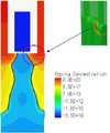
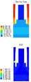
도 13은 종래 기술에 따른 핀 전계효과 트랜지스터의 특성에 대한 가상실험 결과를 도시한다.13 shows the results of a hypothetical experiment on the characteristics of the fin field effect transistor according to the prior art.
도 14는 본 발명의 일 실시예에 따른 핀 전계효과 트랜지스터의 특성에 대한 가상실험 결과를 도시한다.FIG. 14 shows virtual test results of the characteristics of the fin field effect transistor according to the exemplary embodiment of the present invention.
도 15는 도 13 및 도 14의 가상실험 결과에 따른 종래 기술 및 본 발명에 따른 Id-Vg 곡선을 도시한다.FIG. 15 shows Id-Vg curves according to the prior art and the present invention according to the results of the virtual experiments of FIGS. 13 and 14.
본 발명은 반도체 소자 및 그 형성 방법에 관한 것으로, 특히, 기판으로부터 돌출된 핀 형태의 채널을 갖는 전계 효과 트랜지스터 및 그 형성 방법에 관한 것이다.BACKGROUND OF THE INVENTION Field of the Invention The present invention relates to a semiconductor device and a method of forming the same, and more particularly, to a field effect transistor having a fin-shaped channel protruding from a substrate and a method of forming the same.
통상, 반도체 소자의 전계 효과 트랜지스터는 반도체 기판에 서로 이격되어 형성된 소오스/드레인 영역들과, 상기 소오스 영역 및 드레인 영역 사이의 채널영역 상부에 형성된 게이트 전극으로 구성될 수 있다.In general, the field effect transistor of the semiconductor device may include source / drain regions formed on the semiconductor substrate and spaced apart from each other, and a gate electrode formed on the channel region between the source region and the drain region.
반도체 소자의 고집적화 경향에 따라, 트랜지스터의 크기가 점점 감소되어 많은 문제점들이 대두되고 있다. 예를 들면, 채널 길이의 감소로 인하여 소오스/드레인 영역들 간의 펀치스루 특성이 열화되고 있으며, 게이트 전극의 채널영역에 대한 컨트롤 능력(controllability)이 저하되어 누설전류의 량이 증가되고 있다. 특히, 평면 트랜지스터(planar transistor) 구조를 갖고 있는 반도체 소자가 점점 축소되면서 단채널 효과 (short channel effect)가 증가하여 트랜지스터 특성, 즉 온-전류(on-current), 오프-전류(off-current), 서브문턱전압 스윙(subthreshold swing), 드레인 기인 배리어 강하(DIBL:drain-induced barrier lowering) 등의 특성에서 한계를 드러냄에 따라 평면형 트랜지스터 구조의 한계를 극복하기 위해서 최근 다양한 구조의 트랜지스터가 연구되고 있는데 이 중 3차원 구조를 갖는 핀 전계효과 트랜지스터(FinFET;핀펫)가 평면형 트랜지스터를 대체할 유력한 후보로 대두되고 있다. 핀 전계효과 트랜지스터 구조는 기존의 평면형 트랜지스터 구조 대비 서브문턱전압 스윙, DIBL, 바디 효과(body effect), 온 및 오프-전류 등의 특성이 우수한 것으로 보고 되고 있다. 핀 전계효과 트랜지스터는 기판 상에 돌출된 실리콘 핀을 가로지르도록 게이트 전극을 형성한다. 상기 게이트 전극의 아래의 상기 실리콘 핀은 채널영역에 해당하며, 상기 게이트 전극은 상기 실리콘 핀의 상부 및 양측벽들을 지난다. 이로써, 상기 게이트 전극은 상기 채널영역의 상부 및 양측을 컨트롤함으로써, 채널영역을 컨트롤하는 능력이 향상된다. 또한, 상기 채널 영역 양측의 상기 실리콘 핀에 소오스/드레인 영역들이 형성됨으로써, 소오스/드레인 영역들 간의 펀치스루 특성 등이 향상될 수 있다.With the trend toward higher integration of semiconductor devices, the size of transistors is gradually reduced and many problems are raised. For example, the punch-through characteristics between the source and drain regions are deteriorated due to the decrease in the channel length, and the controllability of the channel region of the gate electrode is lowered, thereby increasing the amount of leakage current. In particular, as semiconductor devices having a planar transistor structure become smaller and smaller, short channel effects increase, so that transistor characteristics, that is, on-current and off-current, are increased. In order to overcome the limitations of the planar transistor structure, the transistors of various structures have been recently studied to reveal limitations in characteristics such as subthreshold swing and drain-induced barrier lowering (DIBL). Among them, a fin field effect transistor (FinFET) having a three-dimensional structure has emerged as a potential candidate to replace a planar transistor. The fin field effect transistor structure is reported to have superior characteristics such as subthreshold voltage swing, DIBL, body effect, on and off current compared to the conventional planar transistor structure. The fin field effect transistor forms a gate electrode to cross silicon fins projecting on the substrate. The silicon fin below the gate electrode corresponds to a channel region, and the gate electrode passes over the top and both sidewalls of the silicon fin. As a result, the gate electrode controls the upper and both sides of the channel region, thereby improving the ability to control the channel region. In addition, source / drain regions are formed in the silicon fins at both sides of the channel region, so that punch-through characteristics between the source / drain regions may be improved.
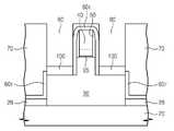
상기 3차원 구조를 갖는 핀 전계효과 트랜지스터가 형성되는 반도체 소자에 관해서는 미국 등록 특허 제6,342,410에 "ABRICATION OF A FIELD EFFECT TRANSISTOR WITH THERE SIDED GATE STRUCTURE ON A SEMICONDUCTOR ON INSULATOR" 의 제목하에 개시되어 있다. 상기 종래의 미국 특허는 도 1의 점선에서 설명되고 있는 것처럼, 일반적인 핀 전계효과 트랜지스터 구조인 삼 게이트 구조(tri-gate)로 형성되는 경우, 핀의 상부와 양측면 게이트로부터의 전기장(electrical field) 집중으로 게이트-기인 드레인 누설전류(Gate-Induced Drain Leakage:GIDL)가 급격히 증가하는 문제가 발생하게 된다. 이 GIDL 성분은 디램에서 정적 유지(static retention) 특성을 열화시킨다.A semiconductor device in which the fin field effect transistor having the three-dimensional structure is formed is disclosed in US Patent No. 6,342,410 under the title of "ABRICATION OF A FIELD EFFECT TRANSISTOR WITH THERE SIDED GATE STRUCTURE ON A SEMICONDUCTOR ON INSULATOR". The conventional US patent, when described as a tri-gate, which is a general fin field effect transistor structure, as described in the dashed line of FIG. As a result, the gate-induced drain leakage current (GIDL) increases rapidly. This GIDL component degrades static retention characteristics in the DRAM.
본 발명의 실시예들은 새로운 구조의 핀 트랜지스터 및 그 형성 방법을 제공한다.Embodiments of the present invention provide a fin transistor having a new structure and a method of forming the same.
본 발명의 일 실시예에 따른 반도체 소자는 기판으로 돌출하며 제1 방향을 따라 신장하며 계단형 핀을 구비한다. 상기 제1 방향과 교차하는 제2 방향을 따라 연장하며 상기 계단형 핀의 고단차 부분의 상부면 및 측면 상에 형성된 게이트 전극이 구비된다.A semiconductor device according to an embodiment of the present invention protrudes into a substrate, extends along a first direction, and includes stepped pins. A gate electrode extending along a second direction crossing the first direction and formed on the top and side surfaces of the high stepped portion of the stepped fin is provided.
본 발명의 다른 실시예에 따른 반도체 소자 형성 방법은 반도체 기판에 핀을 형성하는 단계를 포함한다. 상기 핀의 측면 및 상부면 상에 게이트 전극이 형성된다. 상기 게이트 전극 양측에 노출된 핀이 리세스된다. 상기 리세스된 핀에 불순물 이온이 주입되어 리세스 소오스/드레인 영역이 형성된다.In another embodiment, a method of forming a semiconductor device includes forming a fin on a semiconductor substrate. Gate electrodes are formed on the side and top surfaces of the fins. Fins exposed at both sides of the gate electrode are recessed. Impurity ions are implanted into the recessed fins to form recessed source / drain regions.
본 발명의 또 다른 실시예에 따른 반도체 소자는 기판으로 돌출하며 제1 방향을 따라 신장하며 계단형 핀을 구비한다. 상기 제1 방향과 교차하는 제2 방향을 따라 연장하며 상기 계단형 핀의 고단차 부분의 상부면 및 측면 상에 게이트 전극이 구비된다. 상기 계단형 핀의 고단차 부분 및 저단차 부분을 연결하는 수직 연결부 그리고 상기 게이트 전극의 측면 및 상부면 상에 식각 저지층 패턴이 구비된다. 상기 게이트 전극의 양측의 계단형 핀의 저단차 부분에 리세스 소오스/드레인 영역이 구비된다.A semiconductor device according to another embodiment of the present invention protrudes into a substrate and extends along a first direction and includes stepped pins. A gate electrode is provided on an upper surface and a side surface of the high stepped portion of the stepped fin and extending in a second direction crossing the first direction. An etch stop layer pattern is provided on the vertical connection portion connecting the high step portion and the low step portion of the stepped pin and on the side and top surfaces of the gate electrode. Recess source / drain regions are provided at low step portions of the stepped fins on both sides of the gate electrode.
본 발명의 또 다른 실시예에 따른 반도체 소자 형성 방법은 반도체 기판에 핀을 형성하는 단계를 포함한다. 상기 핀의 측면 및 상부면 상에 게이트 전극이 형성된다. 상기 게이트 전극의 측면 상에 게이트 스페이서가 형성된다. 상기 게이트 스페이서 및 상기 게이트 전극을 식각 마스크로 사용하여 상기 게이트 스페이서 외 측의 핀이 리세스되어 계단형 핀이 형성된다. 상기 계단형 핀의 고단차 부분 및 저단차 부분을 연결하는 수직 연결부을 덮는 보호 스페이서가 형성된다. 불순물 이온이 상기 계단형 핀의 저단차 부분에 주입되어 소오스/드레인 영역이 형성된다.In another embodiment, a method of forming a semiconductor device includes forming a fin on a semiconductor substrate. Gate electrodes are formed on the side and top surfaces of the fins. A gate spacer is formed on the side of the gate electrode. Using the gate spacer and the gate electrode as an etch mask, fins outside the gate spacer are recessed to form stepped fins. A protective spacer is formed covering the vertical connection portion connecting the high step portion and the low step portion of the stepped pin. Impurity ions are implanted into the low stepped portion of the stepped fin to form source / drain regions.
이하, 첨부한 도면들을 참조하여 본 발명이 속하는 기술 분야에서 통상의 지식을 가진 자가 본 발명의 기술적 사상을 용이하게 실시할 수 있을 정도로 상세하게 설명하기 위하여 본 발명의 바람직한 실시 예들을 상세히 설명한다. 그러나 본 발명은 여기서 설명되어 지는 실시 예들에 한정되지 않고 다른 형태로 구체화될 수도 있다. 오히려, 여기서 소개되는 실시 예들은 개시된 내용이 철저하고 완전해질 수 있도록 그리고 당 업자에게 본 발명의 사상이 충분히 전달될 수 있도록 하기 위해 제공되어 지는 것이다. 도면들에 있어서, 층 및 영역들의 두께는 명확성을 기하기 위하여 과장되어 진 것이다. 명세서 전체에 걸쳐서 동일한 참조번호들은 동일한 구성요소들을 나타낸다. 이에 더하여, 명세서 전체에 걸쳐서 "반도체 기판에 형성된다."라는 표현은 "반도체 기판 내에 및/또는 반도체 기판 상에 형성된다."라는 표현에 해당할 수 있다.DETAILED DESCRIPTION Hereinafter, exemplary embodiments of the present invention will be described in detail with reference to the accompanying drawings so that those skilled in the art may easily implement the technical idea of the present invention. However, the present invention is not limited to the embodiments described herein and may be embodied in other forms. Rather, the embodiments introduced herein are provided to ensure that the disclosed contents are thorough and complete, and that the spirit of the present invention to those skilled in the art can be sufficiently delivered. In the drawings, the thicknesses of layers and regions are exaggerated for clarity. Like numbers refer to like elements throughout. In addition, the expression “formed on a semiconductor substrate” throughout the specification may correspond to the expression “formed on a semiconductor substrate and / or on a semiconductor substrate.”
도 2는 본 발명의 일 실시예에 따른 핀 전계효과 트랜지스터를 개략적으로 도시하는 사시도이다. 도 2를 참조하면, 본 발명의 일 실시예에 따른 핀 전계효과 트랜지스터는 기판(20)으로부터 돌출한 핀(30)을 구비한다. 핀(30)은 상부면 및 측면들을 구비한다. 게이트 전극(40)은 게이트 절연막(25)을 사이에 두고 핀(30)의 측면들 및 상부면 상에 형성된다. 게이트 전극(40)의 측벽에는 게이트 스페이서(50)가 구부된다. 도면에서 핀(30)은 x축 방향으로 신장하며, 게이트 전극(40)은 y축 방향으로 신장한다. 이하에서 설명의 편의를 위해서 핀의 상부면에 형성된 게이트 전극을 '상부 게이트 전극(G_top)'이라 칭하고, 핀의 측면들 상에 형성된 게이트 전극을 '측면 게이트 전극(G_side)'이라고 칭할 수 있다. 게이트 전극(40) 양측의 핀 영역에 소오스/드레인 영역(30S/D)이 위치한다. 게이트 전극(40)이 형성되는 핀 영역을 '게이트용 핀'이라 칭하고, 이 게이트용 핀과의 구별을 위해서 소오스/드레인 영역(30S/D)이 형성되는 핀 영역을 '소오스/드레인용 핀'이라고 칭할 수 있다.2 is a perspective view schematically illustrating a fin field effect transistor according to an embodiment of the present invention. Referring to FIG. 2, the fin field effect transistor according to the exemplary embodiment includes a fin 30 protruding from the
본 발명의 일 실시예에 따르면, 핀(30)은 기판(20)을 소정 깊이로 식각하는 것에 의해 형성될 수 있다. 또, 본 발명의 일 실시예에 따르면, 소오스/드레인 영역(30S/D)의 상부면은 상부 게이트 전극(G_Top) 아래의 게이트용 핀의 상부면보다 상대적으로 더 낮다. 즉, 게이트용 핀의 상부면보다 소오스/드레인용 핀의 상부면이 더 낮아 전체적으로 핀(30)의 상부면이 계단 형태를 나타낸다. 이 같은 리세스 소오스/드레인 영역(30S/D)으로 인해, 소오스/드레인 영역(30S/D) 및 게이트 전극(40) 사이의 중첩에 의한 결합성 용량(coupling capacitance)이 감소하고, 게이트 기인 드레인 누설(GIDL)이 감소될 수 있다.According to one embodiment of the present invention, the
도 3 및 도 4를 참조하여 본 발명의 일 실시예에 따른 핀 전계효과 트랜지스터 구조에 대해서 보다 상세히 설명을 하기로 한다. 도 3은 핀을 횡단하는 방향 (도 2의 I-I 선에 대응) 으로의 핀 전계효과 트랜지스터의 수직 단면을 개략적으로 도시하고, 도 4는 핀을 종단하는 방향 (도 2의 II-II 선에 대응) 으로의 핀 전계효과 트랜지스터의 수직 단면을 개략적으로 도시한다. 도 3 및 도 4를 참조하면, 게 이트 전극(40)은 게이트용 핀(30)의 상부면(30C_T) 및 측면들(30C_S)을 감싸도록 형성된다. 게이트 전극(40) 및 핀(30) 사이에는 게이트 절연막(25)이 개재한다. 게이트 전극(40)은 폴리실리콘, 텅스텐 실리사이드, 텅스텐 나이트라이드, 텅스텐, 실리콘 나이트라이드, 또는 이들의 조합으로 형성될 수 있다. 게이트 전극(40)은 실리콘 질화막 같은 캐핑막으로 그 상부면이 보호될 수 있다. 인접한 핀들은 소자분리영역(28)에 의해서 서로 전기적으로 절연된다.A fin field effect transistor structure according to an embodiment of the present invention will be described in more detail with reference to FIGS. 3 and 4. FIG. 3 schematically shows the vertical cross section of the fin field effect transistor in the direction of crossing the pin (corresponding to line II in FIG. 2), and FIG. 4 shows the direction of terminating the fin (corresponding to line II-II in FIG. 2). A vertical cross section of a fin field effect transistor in Fig. 1 is schematically shown. 3 and 4, the
게이트 전극(40)의 양측벽에는 게이트 스페이서(50)가 구비된다. 이 게이트 스페이서(50)는 예를 들어 실리콘 질화막으로 형성될 수 있다. 게이트 스페이서(50) 외측의 소오스/드레인용 핀에 리세스 소오스/드레인 영역(30S/D)이 자기정렬된다. 즉, 게이트 스페이서(50) 외측의 핀이 소정 깊이, 예를 들어 약 150 내지 500Å 식각되어 리세스 소오스/드레인 영역(30S/D)이 형성된다.
도 3을 참조하면, 소오스/드레인 영역(30S/D)의 상부면(30S/D_T)이 게이트용 핀의 상부면(30C_T)보다 더 낮아, 핀(30)이 연장하는 방향 (게이트 전극이 연장하는 방향에 수직인 방향)을 따라 핀(30)의 상부면은 전체적으로 단차를 나타낸다. 즉, 핀(30)의 횡단 방향에 따른 그 단면은 계단형태를 나타낸다. 계단형 핀(30)에 따라 저단차 영역(소오스/드레인용 핀) 및 고단차 영역(게이트용 핀)을 연결하는 계단형 핀(30)의 수직 연결부(35)가 정의된다. 이 수직 연결부(35) 상에 식각 저지층 패턴(60r)이 구비될 수 있다. 이 식각 저지층 패턴(60r)은 또한 스페이서(50)의 측벽에 더 구비될 수 있다. 또한, 이 식각 저지층 패턴(60r)은 게이트 전극(40)의 상부면에도 구비될 수 있다. 이 식각 저지층 패턴(60r)은 소오스/드레인 영 역(30S/D)을 형성하기 위한 이온주입 공정에서 불순물이 계단형 핀(30) 수직 연결부(35)로 확산하는 것을 방지하는 기능을 할 수 있다. 이 계단형 핀(30)의 수직 연결부(35)에 불순물 이온이 주입되는 것이 방지되기 때문에, 상부 게이트 전극(G_Top)에 의한 전기장이 완화되어 게이트 기인 드레인 누설전류(GIDL)를 완화시킬 수 있다.Referring to FIG. 3, the
본 발명의 일 실시예에 따르면, 자기정렬 콘택홀(80)을 구비하는 층간절연막(70)이 더 구비될 수 있다. 자기정렬 콘택홀(80) 내에는 소오스/드레인 영역(30S/D)에 접속하는 자기정렬 콘택 패드(90)가 구비된다. 자기정렬 콘택 패드(90)는 예를 들어 폴리실리콘, 금속 등으로 형성될 수 있다. 또한, 소오스/드레인 영역(30S/D)에는 자기정렬 콘택 패드(90)와의 접촉 저항 특성을 개선하기 위한 실리사이드막이 더 구비될 수 있다.According to one embodiment of the present invention, an
이제 도 5 내지 7을 참조하여 본 발명의 일 실시예에 따른 핀 전계효과 트랜지스터의 형성 방법을 설명한다. 도 5 내지 도 7은 핀을 횡단하는 방향 (도 2의 I-I 선에 대응)에서의 수직 단면들이다. 도 5를 참조하면, 핀(30)을 구비하는 기판(20) 상에 게이트 절연막(25)을 형성한 후, 폴리실리콘, 텅스텐 실리사이드, 텅스텐 나이트라이드, 텅스텐, 실리콘 나이트라이드, 또는 이들의 조합으로 게이트 전극(40)을 형성한다. 게이트 전극(40) 측벽에 게이트 스페이서(50)를 형성한다. 게이트 스페이서(50)는 100 내지 350Å 정도의 실리콘 질화막(SiN)을 증착한 후 에치백 공정을 진행하는 것에 의해서 형성될 수 있다.A method of forming a fin field effect transistor according to an embodiment of the present invention will now be described with reference to FIGS. 5 to 7. 5 to 7 are vertical cross sections in the direction traversing the pins (corresponding to line I-I of FIG. 2). Referring to FIG. 5, after the
핀(30)을 구비하는 기판(20)은 벌크 기판을 사용하거나 실리콘-온-절연 막(SOI) 기판을 사용하여 형성될 수 있다. 벌크 기판을 사용할 경우, 벌크 기판을 소정 깊이 식각하여 원하는 높이를 가지는 실리콘 핀을 형성할 수 있다. 이때, 벌크 기판은 실리콘-게르마늄 기판, 도핑 또는 도핑 되지 않은 실리콘 기판, 에피탁시 성장 기술에 의해 형성된 에피탁시층을 갖는 기판 등이 사용될 수 있다. 핀(30)을 형성한 후 인접한 핀들 사이의 전기적인 분리를 위해서 소자분리막(28)이 형성된다.
도 6을 참조하면, 게이트 스페이서(50)를 형성한 후 그 양측의 소오스/드레인용 핀(30)을 일정 깊이만큼 리세스 시킨다. 이로써 게이트 전극(40) 양측의 소오스/드레인용 핀의 상부면이 게이트용 핀의 상부면 보다 낮아지고 핀(30)은 계단 형태를 나타낸다. 예를 들어 게이트 전극용 핀의 상부면과 소오스/드레인용 핀의 상부면은 150 내지 500Å 정도로 높이 차이가 날 수 있다. 핀 리세스에 따른 식각 손상을 치유하기 위해서 열산화 공정이 진행될 수 있다.Referring to FIG. 6, after forming the
도 7을 참조하여, 리세스된 핀에 불순물 이온을 주입하여 리세스 소오스/드레인 영역(30S/D)을 형성한다. 또, 불순물 이온을 주입하기 전에, 계단형 핀(30)의 수직 연결부(35)를 보호하기 위한 보호 스페이서(55)가 더 형성될 수 있다. 이 보호 스페이서는 실리콘 질화막을 증착한 후 에치백 공정을 진행하는 것에 의해서 형성될 수 있다.Referring to FIG. 7, impurity ions are implanted into the recessed fin to form a recess source /
도 8 내지 도 10을 참조하여 본 발명의 또 다른 실시예에 따른 핀 전계효과 트랜지스터 형성 방법을 설명한다. 앞서 도 5 내지 도 7을 참조하여 설명을 한 방법과는 소오스/드레인 형성 방법에 있어서 차이를 나타낸다. 도 8을 참조하면, 도 5 내지 도 6을 참조하여 설명을 한 방법들을 진행하여 소오스/드레인용 핀을 리세스 시킨 후, 식각 저지층(60) 및 층간절연막(70)을 형성한다. 식각 저지층(60) 및 층간절연막(70)은 서로에 대해서 식각 선택성을 가지는 물질로 형성될 수 있다. 예를 들어 식각 저지층(60)은 50 내지 200Å 정도의 실리콘 질화막으로 형성될 수 있다. 예를 들어, 층간절연막(70)은 USG (Undoped Silicated Glass), HTO (High Temperature Oxide), MTO (Medium Temperature Oxide), TEOS (Tetra Ethyl Ortho Silicate), HDP (High Density Plasma) 등의 비도핑 산화막으로 형성되거나 BPSG (Boro Phospho Silicate Glass), PSG (Phospho Silicate Glasss), PSG (Phospho Silicate Glass), BSG (Boro Silicate Glass), 등의 도핑된 산화막으로 형성될 수 있다. 또는 전술한 막들을 2가지 이상 함께 사용할 수도 있다.A method of forming a fin field effect transistor according to still another embodiment of the present invention will be described with reference to FIGS. 8 to 10. The method described above with reference to FIGS. 5 to 7 shows a difference in the source / drain formation method. Referring to FIG. 8, after the methods described with reference to FIGS. 5 to 6 are performed to recess the source / drain fins, an
식각 저지층(60)은 예를 들어 게이트 전극(40)의 상부면, 게이트 스페이서(50)의 측면, 계단형 핀(30)의 수직 연결부(35), 소오스/드레인용 핀 상에 형성될 수 있다. 층간절연막(70)은 식각저지층(60) 상에 형성된다.The
도 9를 참조하면, 자기정렬 식각 공정을 사용하여 식각 저지층(60)이 노출될 때까지 상기 층간절연막(70)을 식각한다. 이어서, 소오스/드레인용 핀 영역 상에 형성된 식각 저지층을 식각하여 자기정렬 콘택 패드가 형성될 콘택홀(80)을 완성한다. 이 콘택홀(80)은 소오스/드레인용 핀을 노출한다. 이때, 게이트 전극(40)의 양 측벽 및 상부면에는 식각 저지층 패턴(60r)이 잔존한다. 이 잔존하는 식각 저지층 패턴(60r)을 마스크로서 이용하여 이온 주입 공정을 실시하여 게이트 전극(40) 양측의 리세스된 소오스/드레인용 핀 영역에 소오스/드레인 영역(30S/D)을 형성한다. 계단형 핀(30)의 수직 연결부(35) 상에 잔존하는 식각 저지층 패턴(65r)이 형성되어 있어, 소오스/드레인 영역을 형성하기 위한 이온 주입 공정에서 불순물 이온이 계단형 핀(30)의 수직 연결부(35)로 주입되는 것이 방지된다.Referring to FIG. 9, the
도 10을 참조하여, 콘택홀(80)을 채우도록 폴리실리콘 등의 도전막을 형성하여 소오스/드레인 영역(30S/D)에 전기적으로 접속하는 콘택 패드(90)를 형성한다. 예를 들어 콘택홀(80)을 완전히 채우도록 층간절연막(70) 상에 폴리실리콘을 증착한 후, 잔존하는 식각 저지층 패턴(60r)이 노출될 때까지 평탄화 공정 예를 들어 화학적기계적연마(CMP) 또는 에치백 공정을 진행하여 콘택홀(80) 내에 콘택 패드(90)를 형성한다.Referring to FIG. 10, a conductive film such as polysilicon is formed to fill the
도 8 내지 도 10을 참조하여 설명을 한 실시예에서, 콘택홀(80)이 게이트 전극(40)의 상부면도 노출할 경우에 게이트 전극(40)의 상부면 상의 식각 저지층도 제거될 것이다. 이 경우에, 잔존하는 식각 저지층 패턴(60r)은 도 5 내지 도 7의 보호 스페이서(55)에 대응할 것이다.8 to 10, the etch stop layer on the top surface of the
도 11 내지 도 12를 참조하여 본 발명의 또 다른 실시예에 따른 핀 전계효과 트랜지스터 형성 방법을 설명한다. 본 실시예에서는 상승된(elevated) 소오스/드레인 영역을 형성하기 위해 에피탁시 성장 기술을 적용한다. 도 11을 참조하여, 소오스/드레인용 핀을 리세스한 후, 에피탁시 공정기술을 적용하여 게이트 전극(40) 양측의 리세스된 핀 영역 상에 소오스/드레인 영역을 위한 에피탁시층(100)을 형성한다. 이 에피탁시 공정을 적절히 조절하여 소오스/드레인 영역의 높이를 소자 특성에 적합하도록 용이하게 조절할 수 있다. 예를 들어 에피탁시층(100)의 높이가 게 이트용 핀의 상부면보다 더 높게 형성될 수 있다. 이 경우에, 에피탁시층(100)과 게이트 전극(40) 사이에는 게이트 스페이서(50) 및 잔존하는 식각 저지층 패턴(60r)이 개재한다.A method of forming a fin field effect transistor according to still another embodiment of the present invention will be described with reference to FIGS. 11 through 12. In this embodiment, epitaxy growth techniques are applied to form elevated source / drain regions. Referring to FIG. 11, after the source / drain fins are recessed, an epitaxial layer for source / drain regions may be formed on the recessed fin regions on both sides of the
도 12를 참조하여, 이온 주입 공정(110)을 진행하여 에피탁시층(100)에 소오스/드레인 영역(110S/D)을 형성한다. 이 소오스/드레인 영역(110S/D)의 상부면은 게이트 전극(40) 아래 채널영역으로 작용하는 핀의 상부면보다 더 높게 형성될 수 있다.Referring to FIG. 12, the
본 발명의 일 실시예에 따른 리세스 소오스/드레인 영역을 갖는 핀 전계효과 트랜지스터의 특성을 알아보기 위해 가상실험(simulation)을 하였다. 가상실험에서 본 발명의 일 실시예에 따른 핀 전계효과 트랜지스터에 대한 가상 핀 전계효과 트랜지스터를 위해서 소오스/드레인 영역의 리세스를 대략 400 Å 정도로 설정하였으며, 소오스/드레인 영역을 위한 가상 이온 주입 공정을 위한 불순물로서 약 1x10¹³ atoms/cm2 의 인(phosphorous)을 설정하였다. 비교를 위해 도 1에 도시된 것 같은 리세스되지 않은 소오스/드레인 영역을 갖는 통상적인 핀 전계효과 트랜지스터를 위해서도 가상실험을 하였다.A simulation was conducted to investigate the characteristics of the fin field effect transistor having the recess source / drain regions according to the exemplary embodiment of the present invention. In the virtual experiment, the recess of the source / drain region is set to about 400 mW for the virtual fin field effect transistor of the fin field effect transistor according to the embodiment of the present invention, and the virtual ion implantation process for the source / drain region is performed. Phosphorous of about 1x10¹³ atoms / cm2 was set as an impurity. For comparison, a hypothetical experiment was also conducted for a conventional fin field effect transistor with an unrecessed source / drain region as shown in FIG.
도 13은 통상적인 핀 전계효과 트랜지스터의 특성에 대한 가상실험 결과를 도시한다. 도 14는 본 발명의 일 실시예에 따른 핀 전계효과 트랜지스터의 특성에 대한 가상실험 결과를 도시한다.13 shows the results of a hypothetical experiment on the characteristics of a conventional fin field effect transistor. FIG. 14 shows virtual test results of the characteristics of the fin field effect transistor according to the exemplary embodiment of the present invention.
도 13를 참조하면, 통상적인 핀 전계효과 트랜지스터에 대한 가상실험 결과 에서는, 소오스/드레인 영역과 핀 상부의 게이트 전극이 오버랩(overlap)되는 농도가 높은 영역에 BTBT(Band to Band tunneling)가 심각하게 유발되고 이로 인해 GIDL이 유발된 것을 확인 할 수 있다. 도 13에서 농도와 BTBT 생성율(Generation Rate)이 가장 높은 영역은 빨간색이고 가장 낮은 부분은 파란색이다.Referring to FIG. 13, in a virtual test result of a conventional fin field effect transistor, band to band tunneling (BTBT) is severely in a region where the source / drain region and the gate electrode on the upper fin are overlapped with each other. It can be confirmed that this caused the GIDL. In FIG. 13, the region having the highest concentration and BTBT generation rate is red, and the lowest portion is blue.
이에 반해 도 14를 참조하면, 본 발명의 일 실시예에 따른 핀 전계효과 트랜지스터에 대한 가상실험 결과에서는, 소오스/드레인 영역과 게이트용 핀의 상부면의 게이트 전극이 오버랩(overlap)되는 영역의 도핑농도가 거의 관찰되지 않고, BTBT가 관찰되지 않으므로 GIDL이 억제되는 것을 확인할 수 있다. 도 14에서 농도와 BTBT 생성율 (Generation Rate)이 가장 높은 영역은 빨간색이고 가장 낮은 부분은 파란색이다.In contrast, referring to FIG. 14, in a virtual experiment result of the fin field effect transistor according to the exemplary embodiment of the present invention, the doping of the source / drain region and the region where the gate electrode of the upper surface of the gate fin overlaps is overlapped. Since concentration is hardly observed and BTBT is not observed, it can be confirmed that GIDL is suppressed. In FIG. 14, the region having the highest concentration and BTBT generation rate is red, and the lowest portion is blue.
도 15는 도 13 및 도 14의 가상실험 결과에 따른 종래 기술 및 본 발명에 따른 Id-Vg 곡선을 도시한다. 도 15를 참조하면, 본 발명의 실시예에 따른 핀 전계효과 트랜지스터의 경우, Vg < 0 V 에서의 GIDL이 약 2 order이상 억제되는 효과를 나타내는 것을 확인할 수 있다.FIG. 15 shows Id-Vg curves according to the prior art and the present invention according to the results of the virtual experiments of FIGS. 13 and 14. Referring to FIG. 15, in the case of the fin field effect transistor according to the exemplary embodiment of the present invention, it can be seen that the GIDL at Vg <0 V is suppressed by about 2 orders or more.
아래 표 1에 가상실험 결과에 따른 핀 전계효과 트랜지스터의 특성을 정리하였다.Table 1 below summarizes the characteristics of the fin field effect transistors according to the virtual test results.
위 표 1로부터, 본 발명의 실시예들에 따르면, 종래 핀 전계효과 트랜지스터 에 비해서 GIDL이 현저히 감소하였음을 확인할 수 있다. 더 나아가서 본 발명의 실시예들에 따르면, 종래 핀 전계효과 트랜지스터에 비해서 온 전류 특성이 보다 양호하며, DIBL이 감소한 것을 확인할 수 있다. 또, 본 발명의 실시예들에 따르면, 이온 주입 에너지의 크기가 변하더라도, 문턱전압, DIBL, 온 전류 및 GIDL 등의 특성은 크게 변하지 않은 것을 확인할 수 있다.From Table 1 above, according to the embodiments of the present invention, it can be seen that the GIDL is significantly reduced compared to the conventional fin field effect transistor. Furthermore, according to the embodiments of the present invention, it can be seen that the on current characteristic is better than that of the conventional fin field effect transistor, and that the DIBL is reduced. In addition, according to embodiments of the present invention, even if the magnitude of the ion implantation energy, it can be seen that the characteristics of the threshold voltage, DIBL, on current, GIDL, etc. did not change significantly.
본 발명의 실시예들에 따르면 리세스 소오스/드레인 영역에서는 게이트와 소오스/드레인 영역의 오버랩이 리세스된 깊이만큼 게이트용 핀의 상부면의 게이트 전극에서 멀어지게 된다. 따라서 상부 게이트 전극의 영향이 감소되어 GIDL 열화를 크게 감소시킬 것으로 기대된다.According to the exemplary embodiments of the present invention, the overlap between the gate and the source / drain regions in the recess source / drain region is far from the gate electrode on the upper surface of the gate fin by the recessed depth. Therefore, it is expected that the influence of the upper gate electrode is reduced, thereby greatly reducing the GIDL degradation.
Claims (19)
Translated fromKoreanPriority Applications (2)
| Application Number | Priority Date | Filing Date | Title |
|---|---|---|---|
| KR1020060079535AKR100751803B1 (en) | 2006-08-22 | 2006-08-22 | Manufacturing Method of Semiconductor Device |
| US11/892,320US20080048262A1 (en) | 2006-08-22 | 2007-08-22 | Fin field effect transistor and method of forming the same |
Applications Claiming Priority (1)
| Application Number | Priority Date | Filing Date | Title |
|---|---|---|---|
| KR1020060079535AKR100751803B1 (en) | 2006-08-22 | 2006-08-22 | Manufacturing Method of Semiconductor Device |
Publications (1)
| Publication Number | Publication Date |
|---|---|
| KR100751803B1true KR100751803B1 (en) | 2007-08-23 |
Family
ID=38615275
Family Applications (1)
| Application Number | Title | Priority Date | Filing Date |
|---|---|---|---|
| KR1020060079535AExpired - Fee RelatedKR100751803B1 (en) | 2006-08-22 | 2006-08-22 | Manufacturing Method of Semiconductor Device |
Country Status (2)
| Country | Link |
|---|---|
| US (1) | US20080048262A1 (en) |
| KR (1) | KR100751803B1 (en) |
Cited By (1)
| Publication number | Priority date | Publication date | Assignee | Title |
|---|---|---|---|---|
| CN110957220A (en)* | 2018-09-27 | 2020-04-03 | 中芯国际集成电路制造(上海)有限公司 | Semiconductor structure and forming method thereof |
Families Citing this family (24)
| Publication number | Priority date | Publication date | Assignee | Title |
|---|---|---|---|---|
| US7915659B2 (en)* | 2008-03-06 | 2011-03-29 | Micron Technology, Inc. | Devices with cavity-defined gates and methods of making the same |
| US7608495B1 (en) | 2008-09-19 | 2009-10-27 | Micron Technology, Inc. | Transistor forming methods |
| US8310013B2 (en)* | 2010-02-11 | 2012-11-13 | Taiwan Semiconductor Manufacturing Company, Ltd. | Method of fabricating a FinFET device |
| US8278179B2 (en)* | 2010-03-09 | 2012-10-02 | Taiwan Semiconductor Manufacturing Co., Ltd. | LDD epitaxy for FinFETs |
| US9263342B2 (en) | 2012-03-02 | 2016-02-16 | Taiwan Semiconductor Manufacturing Company, Ltd. | Semiconductor device having a strained region |
| CN103839816B (en)* | 2012-11-25 | 2019-04-19 | 中国科学院微电子研究所 | Semiconductor device and method for manufacturing the same |
| KR20140099743A (en) | 2013-02-04 | 2014-08-13 | 삼성전자주식회사 | Semiconductor device and method for fabricating the same |
| CN105027291A (en)* | 2013-03-29 | 2015-11-04 | 英特尔公司 | Transistor architecture with extended recessed spacers and source/drain regions and method of fabrication thereof |
| US9496398B2 (en)* | 2014-01-15 | 2016-11-15 | Taiwan Semiconductor Manufacturing Company, Ltd. | Epitaxial source/drain regions in FinFETs and methods for forming the same |
| KR102157839B1 (en) | 2014-01-21 | 2020-09-18 | 삼성전자주식회사 | Methods of selectively growing source and drain regions of fin field effect transistor |
| US9633906B2 (en)* | 2014-01-24 | 2017-04-25 | International Business Machines Corporation | Gate structure cut after formation of epitaxial active regions |
| EP2908345A1 (en) | 2014-02-13 | 2015-08-19 | IMEC vzw | Contact formation in Ge-containing semiconductor devices |
| US10050118B2 (en) | 2014-05-05 | 2018-08-14 | Globalfoundries Inc. | Semiconductor device configured for avoiding electrical shorting |
| US9391200B2 (en)* | 2014-06-18 | 2016-07-12 | Stmicroelectronics, Inc. | FinFETs having strained channels, and methods of fabricating finFETs having strained channels |
| KR102227128B1 (en)* | 2014-09-03 | 2021-03-12 | 삼성전자주식회사 | Semiconductor device and method for fabricating the same |
| KR102326316B1 (en)* | 2015-04-10 | 2021-11-16 | 삼성전자주식회사 | Semiconductor dievices and methods of manufacturing the same |
| US9741829B2 (en) | 2015-05-15 | 2017-08-22 | Taiwan Semiconductor Manufacturing Co., Ltd. | Semiconductor device and manufacturing method thereof |
| US9685553B2 (en)* | 2015-06-22 | 2017-06-20 | Globalfoundries Inc. | Generating tensile strain in bulk finFET channel |
| CN106910713B (en)* | 2015-12-22 | 2020-08-04 | 中芯国际集成电路制造(北京)有限公司 | Semiconductor device and method of manufacturing the same |
| CN107452792A (en)* | 2016-06-01 | 2017-12-08 | 中芯国际集成电路制造(上海)有限公司 | Semiconductor device and its manufacture method |
| CN108091570B (en)* | 2016-11-23 | 2020-09-04 | 中芯国际集成电路制造(北京)有限公司 | Semiconductor device and method for manufacturing the same |
| US10510751B2 (en) | 2017-08-25 | 2019-12-17 | Taiwan Semiconductor Manufacturing Co., Ltd. | FinFET isolation structure and method for fabricating the same |
| CN111223780B (en)* | 2018-11-26 | 2024-03-19 | 中芯国际集成电路制造(上海)有限公司 | Semiconductor device and forming method thereof |
| CN113838934B (en)* | 2020-06-24 | 2023-08-18 | 中芯国际集成电路制造(上海)有限公司 | Semiconductor structure and forming method thereof |
Citations (3)
| Publication number | Priority date | Publication date | Assignee | Title |
|---|---|---|---|---|
| JPH088430A (en)* | 1994-06-21 | 1996-01-12 | Sony Corp | Mos transistor and its forming method |
| JP2004039694A (en) | 2002-06-28 | 2004-02-05 | Toshiba Corp | Field effect transistor and method of manufacturing the same |
| US20050253193A1 (en) | 2004-04-30 | 2005-11-17 | Taiwan Semiconductor Manufacturing Co. | Method of fabricating a necked finfet device |
Family Cites Families (6)
| Publication number | Priority date | Publication date | Assignee | Title |
|---|---|---|---|---|
| US7074656B2 (en)* | 2003-04-29 | 2006-07-11 | Taiwan Semiconductor Manufacturing Company, Ltd. | Doping of semiconductor fin devices |
| US6867433B2 (en)* | 2003-04-30 | 2005-03-15 | Taiwan Semiconductor Manufacturing Company, Ltd. | Semiconductor-on-insulator chip incorporating strained-channel partially-depleted, fully-depleted, and multiple-gate transistors |
| KR100517559B1 (en)* | 2003-06-27 | 2005-09-28 | 삼성전자주식회사 | Fin field effect transistor and method for forming of fin therein |
| US7224029B2 (en)* | 2004-01-28 | 2007-05-29 | International Business Machines Corporation | Method and structure to create multiple device widths in FinFET technology in both bulk and SOI |
| US7332386B2 (en)* | 2004-03-23 | 2008-02-19 | Samsung Electronics Co., Ltd. | Methods of fabricating fin field transistors |
| US7525160B2 (en)* | 2005-12-27 | 2009-04-28 | Intel Corporation | Multigate device with recessed strain regions |
- 2006
- 2006-08-22KRKR1020060079535Apatent/KR100751803B1/ennot_activeExpired - Fee Related
- 2007
- 2007-08-22USUS11/892,320patent/US20080048262A1/ennot_activeAbandoned
Patent Citations (3)
| Publication number | Priority date | Publication date | Assignee | Title |
|---|---|---|---|---|
| JPH088430A (en)* | 1994-06-21 | 1996-01-12 | Sony Corp | Mos transistor and its forming method |
| JP2004039694A (en) | 2002-06-28 | 2004-02-05 | Toshiba Corp | Field effect transistor and method of manufacturing the same |
| US20050253193A1 (en) | 2004-04-30 | 2005-11-17 | Taiwan Semiconductor Manufacturing Co. | Method of fabricating a necked finfet device |
Cited By (2)
| Publication number | Priority date | Publication date | Assignee | Title |
|---|---|---|---|---|
| CN110957220A (en)* | 2018-09-27 | 2020-04-03 | 中芯国际集成电路制造(上海)有限公司 | Semiconductor structure and forming method thereof |
| CN110957220B (en)* | 2018-09-27 | 2023-04-25 | 中芯国际集成电路制造(上海)有限公司 | Semiconductor structure and forming method thereof |
Also Published As
| Publication number | Publication date |
|---|---|
| US20080048262A1 (en) | 2008-02-28 |
Similar Documents
| Publication | Publication Date | Title |
|---|---|---|
| KR100751803B1 (en) | Manufacturing Method of Semiconductor Device | |
| US7994568B2 (en) | Vertical transistor of semiconductor device and method for forming the same | |
| JP4551811B2 (en) | Manufacturing method of semiconductor device | |
| US7795670B2 (en) | Semiconductor device and method for fabricating the same | |
| KR100476940B1 (en) | Dram memory cell having a gate channel extending vertically from a substrate and method of fabricating the same | |
| US7741673B2 (en) | Floating body memory and method of fabricating the same | |
| US8410547B2 (en) | Semiconductor device and method for fabricating the same | |
| US20090173992A1 (en) | Semiconductor device with improved performance characteristics | |
| US7575964B2 (en) | Semiconductor device employing buried insulating layer and method of fabricating the same | |
| US20070085127A1 (en) | Semiconductor device and method of manufacturing the same | |
| CN100378985C (en) | Semiconductor structure of semiconductor wafer and forming method thereof | |
| US10886181B2 (en) | Semiconductor device | |
| KR20050108916A (en) | Methods of forming a fin field effect transistor using damascene process | |
| CN107819031B (en) | Transistor, forming method thereof and semiconductor device | |
| KR102859797B1 (en) | Semiconductor device and method of manufacturing the same | |
| US7521766B2 (en) | Transistor and method of forming the same | |
| US20080073730A1 (en) | Semiconductor device and method for formimg the same | |
| KR20040002204A (en) | Semiconductor device and method for manufacturing the same | |
| CN116072675A (en) | Semiconductor structure and forming method thereof | |
| KR20080081550A (en) | MOSFET device and its manufacturing method | |
| KR100506455B1 (en) | A method for forming a semiconductor device | |
| CN114914287B (en) | Preparation method of fin field effect transistor | |
| KR20080088095A (en) | Gate Forming Method of Semiconductor Device | |
| KR20100053037A (en) | Transistor controlling short channel effect and the method of manufacturing the same | |
| CN1196581A (en) | Semiconductor structure and forming method thereof |
Legal Events
| Date | Code | Title | Description |
|---|---|---|---|
| A201 | Request for examination | ||
| PA0109 | Patent application | St.27 status event code:A-0-1-A10-A12-nap-PA0109 | |
| PA0201 | Request for examination | St.27 status event code:A-1-2-D10-D11-exm-PA0201 | |
| D13-X000 | Search requested | St.27 status event code:A-1-2-D10-D13-srh-X000 | |
| D14-X000 | Search report completed | St.27 status event code:A-1-2-D10-D14-srh-X000 | |
| E701 | Decision to grant or registration of patent right | ||
| PE0701 | Decision of registration | St.27 status event code:A-1-2-D10-D22-exm-PE0701 | |
| GRNT | Written decision to grant | ||
| PR0701 | Registration of establishment | St.27 status event code:A-2-4-F10-F11-exm-PR0701 | |
| PR1002 | Payment of registration fee | St.27 status event code:A-2-2-U10-U11-oth-PR1002 Fee payment year number:1 | |
| PG1601 | Publication of registration | St.27 status event code:A-4-4-Q10-Q13-nap-PG1601 | |
| PR1001 | Payment of annual fee | St.27 status event code:A-4-4-U10-U11-oth-PR1001 Fee payment year number:4 | |
| PR1001 | Payment of annual fee | St.27 status event code:A-4-4-U10-U11-oth-PR1001 Fee payment year number:5 | |
| R18-X000 | Changes to party contact information recorded | St.27 status event code:A-5-5-R10-R18-oth-X000 | |
| FPAY | Annual fee payment | Payment date:20120801 Year of fee payment:6 | |
| PR1001 | Payment of annual fee | St.27 status event code:A-4-4-U10-U11-oth-PR1001 Fee payment year number:6 | |
| FPAY | Annual fee payment | Payment date:20130731 Year of fee payment:7 | |
| PR1001 | Payment of annual fee | St.27 status event code:A-4-4-U10-U11-oth-PR1001 Fee payment year number:7 | |
| LAPS | Lapse due to unpaid annual fee | ||
| PC1903 | Unpaid annual fee | St.27 status event code:A-4-4-U10-U13-oth-PC1903 Not in force date:20140818 Payment event data comment text:Termination Category : DEFAULT_OF_REGISTRATION_FEE | |
| PC1903 | Unpaid annual fee | St.27 status event code:N-4-6-H10-H13-oth-PC1903 Ip right cessation event data comment text:Termination Category : DEFAULT_OF_REGISTRATION_FEE Not in force date:20140818 | |
| P22-X000 | Classification modified | St.27 status event code:A-4-4-P10-P22-nap-X000 |