KR100750802B1 - Semiconductor device and manufacturing method - Google Patents
Semiconductor device and manufacturing methodDownload PDFInfo
- Publication number
- KR100750802B1 KR100750802B1KR1020060071049AKR20060071049AKR100750802B1KR 100750802 B1KR100750802 B1KR 100750802B1KR 1020060071049 AKR1020060071049 AKR 1020060071049AKR 20060071049 AKR20060071049 AKR 20060071049AKR 100750802 B1KR100750802 B1KR 100750802B1
- Authority
- KR
- South Korea
- Prior art keywords
- insulating layer
- key
- metal
- semiconductor device
- metal wiring
- Prior art date
- Legal status (The legal status is an assumption and is not a legal conclusion. Google has not performed a legal analysis and makes no representation as to the accuracy of the status listed.)
- Expired - Fee Related
Links
Images


Classifications
- H—ELECTRICITY
- H01—ELECTRIC ELEMENTS
- H01L—SEMICONDUCTOR DEVICES NOT COVERED BY CLASS H10
- H01L21/00—Processes or apparatus adapted for the manufacture or treatment of semiconductor or solid state devices or of parts thereof
- H01L21/02—Manufacture or treatment of semiconductor devices or of parts thereof
- H01L21/04—Manufacture or treatment of semiconductor devices or of parts thereof the devices having potential barriers, e.g. a PN junction, depletion layer or carrier concentration layer
- H01L21/18—Manufacture or treatment of semiconductor devices or of parts thereof the devices having potential barriers, e.g. a PN junction, depletion layer or carrier concentration layer the devices having semiconductor bodies comprising elements of Group IV of the Periodic Table or AIIIBV compounds with or without impurities, e.g. doping materials
- H01L21/28—Manufacture of electrodes on semiconductor bodies using processes or apparatus not provided for in groups H01L21/20 - H01L21/268
- H—ELECTRICITY
- H01—ELECTRIC ELEMENTS
- H01L—SEMICONDUCTOR DEVICES NOT COVERED BY CLASS H10
- H01L23/00—Details of semiconductor or other solid state devices
- H01L23/544—Marks applied to semiconductor devices or parts, e.g. registration marks, alignment structures, wafer maps
- H—ELECTRICITY
- H01—ELECTRIC ELEMENTS
- H01L—SEMICONDUCTOR DEVICES NOT COVERED BY CLASS H10
- H01L2924/00—Indexing scheme for arrangements or methods for connecting or disconnecting semiconductor or solid-state bodies as covered by H01L24/00
- H01L2924/0001—Technical content checked by a classifier
- H01L2924/0002—Not covered by any one of groups H01L24/00, H01L24/00 and H01L2224/00
- H—ELECTRICITY
- H10—SEMICONDUCTOR DEVICES; ELECTRIC SOLID-STATE DEVICES NOT OTHERWISE PROVIDED FOR
- H10F—INORGANIC SEMICONDUCTOR DEVICES SENSITIVE TO INFRARED RADIATION, LIGHT, ELECTROMAGNETIC RADIATION OF SHORTER WAVELENGTH OR CORPUSCULAR RADIATION
- H10F39/00—Integrated devices, or assemblies of multiple devices, comprising at least one element covered by group H10F30/00, e.g. radiation detectors comprising photodiode arrays
- H10F39/80—Constructional details of image sensors
Landscapes
- Engineering & Computer Science (AREA)
- Physics & Mathematics (AREA)
- Condensed Matter Physics & Semiconductors (AREA)
- General Physics & Mathematics (AREA)
- Computer Hardware Design (AREA)
- Microelectronics & Electronic Packaging (AREA)
- Power Engineering (AREA)
- Manufacturing & Machinery (AREA)
- Internal Circuitry In Semiconductor Integrated Circuit Devices (AREA)
Abstract
Translated fromKoreanDescription
Translated fromKorean도 1a는 종래 기술에 의한 반도체 소자의 오버레이 키(Overlay Key)를 나타내는 도면이다.1A is a diagram illustrating an overlay key of a semiconductor device according to the prior art.
도 1b 내지 도 1f는 종래기술에 의한 반도체 소자의 제조공정을 나타내는 단면도이다.1B to 1F are cross-sectional views illustrating a manufacturing process of a semiconductor device according to the prior art.
도 1g는 종래기술에 의한 반도체 소자의 제조공정의 문제점을 나타내는 도면이다.1G is a view showing a problem of the manufacturing process of a semiconductor device according to the prior art.
도 2a 내지 도 2e는 본 발명의 실시예에 따른 반도체 소자의 제조공정을 나타내는 단면도이다.2A through 2E are cross-sectional views illustrating a process of manufacturing a semiconductor device in accordance with an embodiment of the present invention.
도 2f는 본 발명의 실시예에 따른 반도체 소자의 효과를 나타내는 도면이다.2F is a view showing the effect of the semiconductor device according to the embodiment of the present invention.
<도면의 주요 부분에 대한 설명>Description of the main parts of the drawing
110: 제1 감광막 120: 제1 절연층110: first photosensitive film 120: first insulating layer
130: 잔여 비아플러그 140: 금속배선130: remaining via plug 140: metal wiring
150: 제2 감광막 160: 제2 절연층150: second photosensitive film 160: second insulating layer
본 발명은 반도체 소자 및 그 제조방법에 관한 것으로, 상세하게는 씨모스이미지 센서 및 그 제조방법에 관한 것이다.The present invention relates to a semiconductor device and a method of manufacturing the same, and more particularly to a CMOS image sensor and a method of manufacturing the same.
도 1a는 종래 기술에 의한 반도체 소자의 오버레이 키(Overlay Key)를 나타내는 도면이다.1A is a diagram illustrating an overlay key of a semiconductor device according to the prior art.
상기 오버레이 키는 전 공정에서 형성되는 외부 키(outer key)(70)와 후 공정에서 형성되는 내부 키(Inner key)(80)로 이루어진 것으로 일반적으로 사진 공정 진행 후 정렬상태를 측정하기 위한 도구로써, 통상 스크라이브 레인(scribe lane)에 형성된다.The overlay key is composed of an
도 1b 내지 도 1f는 종래기술에 의한 반도체 소자의 제조공정을 나타내는 단면도이다.1B to 1F are cross-sectional views illustrating a manufacturing process of a semiconductor device according to the prior art.
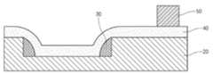
우선, 도 1b는 외부 키(70)가 형성된 것을 나타낸 것으로, 도 1a의 화살표 부분(I-I라인)의 단면도이다. 도 1b에 도시된 바와 같이, 반도체 기판(미도시)상에 제1 절연층(20)을 적층하고 평탄화한 후 사진 및 식각 공정을 통하여 외부 키(70)가 될 부분의 제1 절연층(20)을 식각한다.First, FIG. 1B shows that the
다음으로, 도 1c에 도시된 바와 같이, 제1 금속배선(40)을 적층하는 공정을 진행한다. 즉, 도 1b의 결과물 상에 텅스텐(W)(30)을 적층 한 후 CMP 공정을 이용하여 비아홀 만을 매립한 후 이어서 제1 금속배선(40)을 적층한다.Next, as shown in FIG. 1C, a process of stacking the
그런데, 이때 비아홀을 제외한 부분의 텅스텐(30)은 모두 제거가 되어야하나 외부 키(70)의 측벽에 단차가 형성된 부분에서는 텅스텐(30)이 모두 제거되지 않고 텅스텐(30)의 일부(Residue)가 남아있게 된다.In this case, all of the
다음으로, 도 1d에 도시된 바와 같이, 감광막(50) 패턴으로 내부 키(80)를 형성한다. 즉, 도 1c의 결과물 상에 감광막(50)을 전면 도포한 후 사진공정을 통하여 내부 키(80)가 형성될 부분의 감광막(50)이 남도록 한다.Next, as shown in FIG. 1D, the
상기의 사진공정이 끝나면 내부 키(80) 부분은 감광막(50)이 남게 되어, 전 공정에서 형성된 외부 키(70)의 제1 절연층(20)의 단차 부분과, 내부 키(80)의 감광막(50)의 단차를 이용하여 정렬상태를 측정하게 된다.When the photographing process is completed, the
다음으로, 도 1e에 도시된 바와 같이, 제1 금속배선(40) 패터닝 및 제2 절연층(60) 적층 공정을 진행한다. 즉, 도 1d의 결과물을 식각하여 제1 금속배선(40)을 형성한 후 그 결과물 상에 제2 절연층(60)을 적층한다.Next, as shown in FIG. 1E, the
다음으로, 도 1f는 종래기술의 문제점을 나타낸다.Next, FIG. 1F illustrates a problem of the prior art.
즉, 도 1e와 같이 제2 절연층(60)을 적층 할 때 외부 키(70)로 만들어졌던 제1 절연층(20)의 단차로 인해 측벽에 남아있던 텅스텐(30)으로 인하여 접촉이 불량해지고, 결국 제2 절연층(60)은 그 부분에서 갈라지면서(cracking) 동시에 들뜸현상(lifting)(A)을 일으키게 된다. 이는 제2 절연층(60)과 비아플러그용 금속인 텅스텐(30)과의 접촉성이 매우 좋지 못하기 때문이다.That is, due to the step of the first insulating
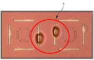
다음으로, 도 1g는 실제 공정진행 중 들뜸현상(A)이 발생한 상황을 나타낸다. 즉, 전 공정에서 형성되는 외부 키(70) 부근에서 제2 절연층(60)이 타원형 형태로 들뜬(lifting) 것을 볼 수 있다.Next, Figure 1g shows a situation in which the lifting phenomenon (A) occurred during the actual process progress. That is, it can be seen that the second insulating
앞에서 설명한 바와 같이, 종래의 기술에서는 오버레이 키에서 절연층의 들 뜸현상이 발생하며, 이와 같이 들뜬 절연층 조각들은 다른 부분으로 전이되어 제품의 신뢰성을 떨어뜨리는 문제가 있다.As described above, in the prior art, the lifting of the insulating layer occurs in the overlay key, and thus the pieces of the insulating layer are transferred to other parts, thereby degrading the reliability of the product.
또한, 반도체 소자, 특히 CMOS 이미지 센서(Image sensor)와 같이 좋은 이미지를 얻어야하는 제품에서는 절연층의 들뜸현상이 발생하는 경우 이미지에 디펙트(defect)가 형성되게 되는 치명적인 결함이 발생하는 문제가 있다.In addition, a semiconductor device, especially a product that needs to obtain a good image, such as a CMOS image sensor, has a problem in that a fatal defect that causes defects in the image occurs when the insulating layer is lifted. .
본 발명에 따른 반도체 소자 및 그 제조방법은 오버레이 키를 형성할 때, 제2 절연층이 텅스텐 잔여물(residue)과 직접 접촉(adhesion)함으로써 발생하는 들뜸현상 등을 방지하는 것을 목적으로 한다.A semiconductor device and a method of manufacturing the same according to the present invention aim to prevent the lifting phenomenon caused by the direct contact with the tungsten residue when forming the overlay key.
상기의 목적을 달성하기 위한 본 발명에 따른 반도체 소자는 외부 키(outer key) 기능을 하는 비아홀을 포함하는 제1 절연층; 상기 비아홀 내부에 제1 금속을 매립하여 형성되는 비아플러그가 일부 제거되고 남은 잔여 비아플러그; 상기 잔여 비아플러그를 포함하는 제1 절연층 상에 제2 금속을 적층 하되, 내부 키가 형성될 부분이 식각되어 상기 제1 절연층을 일부 노출하는 금속배선; 및 상기 금속배선과 노출된 제1 절연층 상에 적층되는 제2 절연층;을 포함하는 것을 특징으로 한다.According to another aspect of the present invention, there is provided a semiconductor device including: a first insulating layer including a via hole functioning as an outer key; A remaining via plug remaining after the via plug formed by filling the first metal is partially embedded in the via hole; A metal wiring on which the second metal is stacked on the first insulating layer including the remaining via plugs, the portion of which an internal key is to be etched to partially expose the first insulating layer; And a second insulating layer stacked on the metal wiring and the exposed first insulating layer.
또한, 상기의 목적을 달성하기 위한 본 발명에 따른 반도체 소자의 제조방법은 기판의 스크라이브 레인(scribe lane) 상에 제1 절연층을 형성하는 단계; 상기 제1 절연층을 제1 감광막을 사용하여 식각함으로써 외부 키(outer key)의 기능을 하는 비아홀을 형성하는 단계; 상기 비아홀 내부에 제1 금속을 매립하여 비아플러 그를 형성하는 단계; 상기 비아플러그의 일부를 제거하는 단계; 상기 잔여 비아플러그를 포함하는 제1 절연층 상에 제2 금속을 이용하여 금속배선을 적층단계; 상기 금속배선 상에 제2 감광막을 형성하는 단계; 상기 제2 감광막을 패터닝하여 내부 키가 형성되도록 하되, 상기 내부 키 부분에 제2 감광막이 남지 않도록 하는 사진공정단계; 상기 제2 감광막을 식각마스크로 하여 내부 키 부분의 상기 금속배선을 식각하여 상기 제1 절연막의 일부를 노출하는 단계; 및 상기 금속배선과 노출된 제1 절연층 상에 제2 절연층을 적층하는 단계;를 포함하는 것을 특징으로 한다.In addition, a method of manufacturing a semiconductor device according to the present invention for achieving the above object comprises the steps of forming a first insulating layer on a scribe lane of the substrate; Forming a via hole functioning as an outer key by etching the first insulating layer using a first photosensitive film; Filling a first metal in the via hole to form a via plug; Removing a portion of the viaplug; Stacking metal wires on the first insulating layer including the remaining via plugs using a second metal; Forming a second photoresist film on the metal wiring; A photolithography step of patterning the second photoresist film so that an internal key is formed, but not leaving a second photoresist film on the inner key portion; Etching the metal wiring of an inner key portion using the second photoresist as an etch mask to expose a portion of the first insulating film; And laminating a second insulating layer on the metal wiring and the exposed first insulating layer.
이와 같은 본 발명에 의하면 오버레이 키의 내부 키를 형성 할 때, 금속배선이 전 공정에서 형성된 외부 키를 감싸도록 하여 종래기술에서 문제되었던 절연층의 들뜸(lifting)현상을 방지하여 신뢰성 있는 반도체 장치를 구현할 수 있는 장점이 있다.According to the present invention, when forming the inner key of the overlay key, the metal wiring surrounds the external key formed in the previous process to prevent the lifting phenomenon of the insulating layer, which has been a problem in the prior art, thereby providing a reliable semiconductor device. There are advantages to implement.
이하, 본 발명의 실시예에 따른 반도체 소자 및 그 제조방법 첨부된 도면을 참조하여 상세히 설명한다.Hereinafter, a semiconductor device and a method of manufacturing the same according to an embodiment of the present invention will be described in detail with reference to the accompanying drawings.
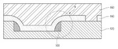
우선, 본 발명의 실시예에 따른 반도체 소자를 도 2e를 참조하여 설명한다.First, a semiconductor device according to an exemplary embodiment of the present invention will be described with reference to FIG. 2E.
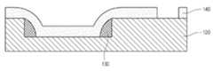
본 발명의 실시예에 따른 반도체 소자는 외부 키(outer key)를 포함하는 제1 절연층(120), 잔여 비아플러그(130), 금속배선(140), 제2 절연층(160)을 포함하는 것을 특징으로 한다.In an embodiment, a semiconductor device may include a first
본 발명에 실시예에 따른 반도체 소자는 기판(미도시)의 스크라이브 레인(scribe lane)(미도시) 상에 형성되는 제1 절연층(120), 제2 절연층(160)을 포함하는 반도체 소자에 관한 것이다.A semiconductor device according to an embodiment of the present invention includes a semiconductor device including a first
상기 외부 키(outer key)를 포함하는 제1 절연층(120)은 상기 제1 절연층(120)을 제1 감광막(110)로 식각하여 비아홀을 형성함으로써 만들어진다.The first
다음으로 상기 잔여 비아플러그(130)는 상기 비아홀 내부에 제1 금속을 매립하여 형성되는 비아플러그가 일부 제거되고 남은 잔여 비아플러그이다. 상기 제1 금속은 W, Al, Cu, Ti, TiN 등을 사용할 수 있다.Next, the remaining via
상기 비아홀 내부에 제1 금속을 매립한다. 그 후 상기 제1 금속을 평탄화 공정, 예를 들어 CMP 공정을 진행하여 비아홀 만을 매립한다. 이후 상기 비아홀에 매립된 제1 금속을 제거하게 되는 데 비아홀의 측벽단차로 인해 제1 금속이 모두 제거되지 못하고 일부 잔여 비아플러그(130)가 남게된다.A first metal is buried in the via hole. Thereafter, the first metal is planarized, for example, a CMP process, to fill only the via holes. Thereafter, the first metal buried in the via hole is removed. However, due to the sidewall step of the via hole, all of the first metal is not removed and some residual via
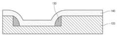
다음으로, 상기 금속배선(140)은 상기 잔여 비아플러그(130)를 포함하는 제1 절연층(120) 상에 제2 금속을 적층 하되, 내부 키가 형성될 부분이 식각되어 상기 제1 절연층(120)을 일부 노출하는 금속배선이다.Next, the
상기 제2 금속은 Al, W, Cu, Ti, TiN, W, WN, TiW, TaW 등을 사용할 수 있다.The second metal may be Al, W, Cu, Ti, TiN, W, WN, TiW, TaW and the like.
또한, 본 발명의 실시예에 따른 반도체 소자는 상기 금속배선(140) 하측에 Ti/TiN, TiW 또는 TiSi2 등을 이용한 장벽금속층을 더 포함할 수 있다.In addition, the semiconductor device according to the embodiment of the present invention may further include a barrier metal layer using Ti / TiN, TiW, or TiSi2 under the
다음으로, 상기 제2 절연층(160)은 상기 금속배선(140)과 노출된 제1 절연층(120) 상에 적층되는 제2 절연층이다.Next, the second insulating
이상에서 설명한 바와 같이 본 발명에 따른 반도체 소자에 의하면, 오버레이 키의 내부 키를 형성 할 때, 금속배선이 전 공정에서 형성된 외부 키를 감싸도록 하여 종래기술에서 문제되었던 절연층의 들뜸(lifting)현상을 방지하여 신뢰성 있는 반도체 장치를 구현할 수 있는 효과가 있다.As described above, according to the semiconductor device according to the present invention, when forming the inner key of the overlay key, the metal wiring surrounds the external key formed in the previous step, so that the lifting phenomenon of the insulating layer, which has been a problem in the prior art, has been raised. There is an effect that can implement a reliable semiconductor device by preventing the.
또한, 본 발명에 의하면 특히 영상특성에 치명적 결함을 주었던 들뜸현상을 방지함으로써 CMOS 이미지 센서의 영상특성을 현저히 개선할 수 있는 효과가 있다.In addition, according to the present invention, it is possible to remarkably improve the image characteristics of the CMOS image sensor by preventing the floating phenomenon, which causes a fatal defect in the image characteristics.
이하, 본 발명의 실시예에 따른 반도체 소자의 제조방법을 첨부 도면을 참조하여 상세히 설명한다.Hereinafter, a method of manufacturing a semiconductor device according to an embodiment of the present invention will be described in detail with reference to the accompanying drawings.
본 발명의 실시예에 따른 반도체 소자의 제조방법은 제1 절연층을 형성하는 단계, 비아홀을 형성하는 단계, 비아플러그를 형성하는 단계, 비아플러그의 일부를 제거하는 단계, 금속배선을 적층하는 단계, 제2 감광막을 형성하는 단계, 제2 감광막에 대한 사진공정단계, 제1 절연막의 일부를 노출하는 단계, 제2 절연층을 적층하는 단계를 포함하는 것을 특징으로 한다.A method of manufacturing a semiconductor device according to an embodiment of the present invention includes the steps of forming a first insulating layer, forming a via hole, forming a via plug, removing a portion of the via plug, and stacking metal wires. And forming a second photoresist film, performing a photolithography process on the second photoresist film, exposing a portion of the first insulating film, and stacking a second insulating layer.
우선, 제1 절연층(120)을 형성하는 단계는 도 2a에 도시된 바와 같이, 기판(미도시)의 스크라이브 레인(scribe lane)(미도시) 상에 제1 절연층(120)을 형성하는 단계이다. 본 발명에 따른 실시예에서는 상기 제1 층간절연층을 평탄화하는 공정, 예를 들어 CMP 공정을 진행하는 단계를 더 포함할 수 있다.First, forming the first insulating
그 후 상기 제1 절연층(120)을 제1 감광막(110)를 사용하여 식각함으로써 외부 키(outer key)의 기능을 하는 비아홀을 형성한다.Thereafter, the first insulating
다음으로, 비아플러그를 형성하는 단계는 도 2b에 도시된 바와 같이, 상기 비아홀 내부에 소정의 제1 금속을 매립하여 비아플러그를 형성하는 단계이다. 상기 제1 금속은 W, Al, Cu, Ti, TiN 등을 사용할 수 있다.Next, the forming of the via plug is a step of forming the via plug by embedding a predetermined first metal in the via hole, as shown in FIG. 2B. The first metal may be W, Al, Cu, Ti, TiN or the like.
본 발명에 따른 실시예에서는 제1 금속을 매립한 후 상기 제1 금속을 평탄화 공정, 예를 들어 CMP 공정을 진행하여 비아홀 만을 매립할 수 있다.In the embodiment of the present invention, after filling the first metal, the first metal may be planarized, for example, a CMP process, to fill only the via hole.
다음으로, 비아플러그의 일부를 제거하는 단계는 상기 비아홀에 매립된 제1 금속을 제거하게 되는 데 비아홀의 측벽단차로 인해 제1 금속이 모두 제거되지 못하고 일부 잔여 비아플러그(130)가 남게된다.Next, the removing of the part of the via plug removes the first metal embedded in the via hole. However, due to the sidewall step of the via hole, not all of the first metal is removed and some residual via
다음으로, 금속배선을 적층하는 단계는 상기 잔여 비아플러그(130)를 포함하는 제1 절연층(120) 상에 제2 금속을 이용하여 금속배선(140)을 적층단계이다. 이때, 상기 제2 금속은 Al, W, Cu, Ti, TiN, W, WN, TiW, TaW 등을 이용하여 적층할 수 있다.Next, the stacking of the metal wires is a step of stacking the
또한, 본 발명의 실시예에 따른 반도체 소자의 제조방법은 상기 금속배선(140) 하측에 Ti/TiN, TiW 또는 TiSi2 등을 이용한 장벽층을 형성하는 단계를 더 포함할 수 있다.In addition, the method of manufacturing a semiconductor device according to an exemplary embodiment of the present invention may further include forming a barrier layer using Ti / TiN, TiW, TiSi2 , or the like below the
다음으로, 제2 감광막을 형성하는 단계 및 제2 감광막에 대한 사진공정단계는 도 2c에 도시된 바와 같이, 상기 금속배선(140) 상에 제2 감광막(150)을 형성하고, 상기 제2 감광막(150)을 패터닝하여 내부 키가 동시에 형성되도록 하되, 상기 내부 키 부분에 제2 감광막(150)이 남지 않도록 하는 단계이다.Next, the forming of the second photoresist film and the photolithography process for the second photoresist film include forming a
이를 상세히 설명하면, 상기 사진공정이 끝나면 내부 키 부분의 제2 감광막(150)을 제거하고, 전 공정에서 형성된 외부 키의 제1 절연층(120)의 단차 부분과, 내부 키의 제2 감광막(150)의 단차를 이용하여 정렬상태를 측정하게 된다.In detail, when the photographing process is completed, the second
특히, 본 발명에서는 종래 기술과 달리 도 2b의 결과물상에 제2 감광막(150) 을 전면 도포한 후 사진 공정을 통하여 내부 키가 형성될 부분의 제2 감광막(150)이 제거되도록 함에 그 특징이 있다.In particular, in the present invention, unlike the prior art, the second
즉, 본 발명은 상기 외부 키와 내부 키를 형성하는 단계에 있어서, 상기 외부 키가 형성될 부분의 제1 감광막(110)에 대한 제1 마스크(미도시)의 극성(mask polarity)과 내부 키가 형성될 부분의 제2 감광막(150)에 대한 제2 마스크(미도시)의 극성이 서로 화이트(whtie)로 극성을 가지게 하여 감광막이 제거되는 것을 특징으로 한다. 물론, 이때의 상기 제1 감광막(110) 및 제2 감광막(150)은 양성 감광막인 경우의 예이다. 상기 마스크의 극성이 화이트라함은 마스크에서 외부 키가 형성될 부분과 내부 키가 형성될 부분에 빛이 통과하도록 마스크 패턴이 형성된 것을 의미한다.That is, in the forming of the external key and the internal key, the present invention may include a mask polarity and an internal key of a first mask (not shown) with respect to the
다른 예로, 상기 제1 감광막(110) 및 제2 감광막(150)은 음성 감광막인 경우에는 상기 제1 마스크와 제2 마스크의 극성은 다크(Dark)일 수 있다. 상기 마스크의 극성이 다크라함은 마스크에서 외부 키가 형성될 부분과 내부 키가 형성될 부분에 빛이 통과하지 못하도록 마스크 패턴이 형성된 것을 의미한다.As another example, when the
다음으로, 제1 절연막의 일부를 노출하는 단계는 도 2d에 도시된 바와 같이, 상기 제2 감광막(150)을 식각마스크로 하여 내부 키 부분의 상기 금속배선(140)을 식각하여 제1 절연층(120)의 일부를 노출하는 단계이다.Next, exposing a portion of the first insulating film may etch the
다음으로, 제2 절연층을 적층하는 단계는 도 2e에 도시된 바와 같이, 상기 금속배선(140)과 노출된 제1 절연층(120) 상에 제2 절연층(160)을 적층하는 단계이다.Next, the stacking of the second insulating layer is a step of stacking the second insulating
이상의 실시예에서 보듯이, 금속배선(140)이 잔여 비아플러그(130)를 감싸고 있어, 제2 절연층(160)이 적층될 때 제2 절연층(160)이 잔여 비아플러그(130)와 만나게 되지 않으므로 접촉이 나빠지는 것을 방지할 수 있다.As shown in the above embodiment, the
따라서 제2 절연층(160)의 들뜸(lifting)현상을 개선할 수 있는 효과가 있다.Therefore, the lifting phenomenon of the second insulating
도 2f에 도시된 바와 같이, 제2 절연층(160)이 외부 키 주변에서 들뜸현상이 발생하지 않음으로써 제2 절연층(160)이 깨끗하게 적층된 것을 볼 수 있다.As shown in FIG. 2F, the second insulating
이상에서 설명한 본 발명은 전술한 실시예 및 도면에 의해 한정되는 것이 아니고, 본 발명의 기술적 사상을 벗어나지 않는 범위 내에서 여러 가지 치환, 변형 및 변경할 수 있다는 것은 본 발명이 속하는 기술 분야에서 통상의 지식을 가진 자에게 있어 명백할 것이다.The present invention described above is not limited to the above-described embodiments and drawings, and it is common knowledge in the art that various substitutions, modifications, and changes can be made without departing from the technical spirit of the present invention. It will be apparent to those who have
이상에서 설명한 바와 같이 본 발명에 따른 반도체 소자 및 그 제조방법에 의하면, 오버레이 키의 내부 키를 형성 할 때, 금속배선이 전 공정에서 형성된 외부 키를 감싸도록 하여 종래기술에서 문제되었던 절연층의 들뜸(lifting)현상을 방지하여 신뢰성 있는 반도체 장치를 구현할 수 있는 효과가 있다.As described above, according to the semiconductor device and the manufacturing method thereof according to the present invention, when the inner key of the overlay key is formed, the metal wiring surrounds the external key formed in the previous step, thereby lifting the insulating layer that has been a problem in the prior art. There is an effect that can implement a reliable semiconductor device by preventing the (lifting) phenomenon.
또한, 본 발명에 의하면 특히 영상특성에 치명적 결함을 주었던 들뜸현상을 방지함으로써 CMOS 이미지 센서의 영상특성을 현저히 개선할 수 있는 효과가 있다.In addition, according to the present invention, it is possible to remarkably improve the image characteristics of the CMOS image sensor by preventing the floating phenomenon, which causes a fatal defect in the image characteristics.
Claims (9)
Translated fromKoreanPriority Applications (3)
| Application Number | Priority Date | Filing Date | Title |
|---|---|---|---|
| KR1020060071049AKR100750802B1 (en) | 2006-07-27 | 2006-07-27 | Semiconductor device and manufacturing method |
| US11/828,688US20080023736A1 (en) | 2006-07-27 | 2007-07-26 | Semiconductor Device and Method for Manufacturing the Same |
| CNA2007101367817ACN101114631A (en) | 2006-07-27 | 2007-07-27 | Semiconductor device and manufacturing method thereof |
Applications Claiming Priority (1)
| Application Number | Priority Date | Filing Date | Title |
|---|---|---|---|
| KR1020060071049AKR100750802B1 (en) | 2006-07-27 | 2006-07-27 | Semiconductor device and manufacturing method |
Publications (1)
| Publication Number | Publication Date |
|---|---|
| KR100750802B1true KR100750802B1 (en) | 2007-08-20 |
Family
ID=38614968
Family Applications (1)
| Application Number | Title | Priority Date | Filing Date |
|---|---|---|---|
| KR1020060071049AExpired - Fee RelatedKR100750802B1 (en) | 2006-07-27 | 2006-07-27 | Semiconductor device and manufacturing method |
Country Status (3)
| Country | Link |
|---|---|
| US (1) | US20080023736A1 (en) |
| KR (1) | KR100750802B1 (en) |
| CN (1) | CN101114631A (en) |
Families Citing this family (1)
| Publication number | Priority date | Publication date | Assignee | Title |
|---|---|---|---|---|
| KR102077150B1 (en)* | 2013-09-16 | 2020-02-13 | 삼성전자주식회사 | Method for manufacturing semiconductor devices |
Citations (2)
| Publication number | Priority date | Publication date | Assignee | Title |
|---|---|---|---|---|
| KR19990070753A (en)* | 1998-02-24 | 1999-09-15 | 윤종용 | A semiconductor device having a trench alignment key and a method of manufacturing the same |
| KR20010026933A (en)* | 1999-09-09 | 2001-04-06 | 박종섭 | Method of manufacturing semiconductor memory device |
Family Cites Families (9)
| Publication number | Priority date | Publication date | Assignee | Title |
|---|---|---|---|---|
| US6232228B1 (en)* | 1998-06-25 | 2001-05-15 | Samsung Electronics Co., Ltd. | Method of manufacturing semiconductor devices, etching composition for manufacturing semiconductor devices, and semiconductor devices made using the method |
| US6218203B1 (en)* | 1999-06-28 | 2001-04-17 | Advantest Corp. | Method of producing a contact structure |
| US6924090B2 (en)* | 2001-08-09 | 2005-08-02 | Neomax Co., Ltd. | Method of recording identifier and set of photomasks |
| US6774452B1 (en)* | 2002-12-17 | 2004-08-10 | Cypress Semiconductor Corporation | Semiconductor structure having alignment marks with shallow trench isolation |
| WO2005010975A1 (en)* | 2003-06-24 | 2005-02-03 | International Business Machines Corporation | Planar magnetic tunnel junction substrate having recessed alignment marks |
| US7221034B2 (en)* | 2004-02-27 | 2007-05-22 | Infineon Technologies Ag | Semiconductor structure including vias |
| US7196429B2 (en)* | 2004-04-26 | 2007-03-27 | Macronix International Co., Ltd. | Method of reducing film stress on overlay mark |
| US7192845B2 (en)* | 2004-06-08 | 2007-03-20 | Macronix International Co., Ltd. | Method of reducing alignment measurement errors between device layers |
| JP4373874B2 (en)* | 2004-08-04 | 2009-11-25 | 富士通マイクロエレクトロニクス株式会社 | Semiconductor device, semiconductor substrate |
- 2006
- 2006-07-27KRKR1020060071049Apatent/KR100750802B1/ennot_activeExpired - Fee Related
- 2007
- 2007-07-26USUS11/828,688patent/US20080023736A1/ennot_activeAbandoned
- 2007-07-27CNCNA2007101367817Apatent/CN101114631A/enactivePending
Patent Citations (2)
| Publication number | Priority date | Publication date | Assignee | Title |
|---|---|---|---|---|
| KR19990070753A (en)* | 1998-02-24 | 1999-09-15 | 윤종용 | A semiconductor device having a trench alignment key and a method of manufacturing the same |
| KR20010026933A (en)* | 1999-09-09 | 2001-04-06 | 박종섭 | Method of manufacturing semiconductor memory device |
Also Published As
| Publication number | Publication date |
|---|---|
| US20080023736A1 (en) | 2008-01-31 |
| CN101114631A (en) | 2008-01-30 |
Similar Documents
| Publication | Publication Date | Title |
|---|---|---|
| US20120313256A1 (en) | Non-Hierarchical Metal Layers for Integrated Circuits | |
| JP2009038061A (en) | Semiconductor wafer and manufacturing method of semiconductor device | |
| JPH1154627A (en) | Semiconductor element fuse forming method and semiconductor device having the fuse | |
| US7241682B2 (en) | Method of forming a dual damascene structure | |
| KR100546099B1 (en) | Metal wiring formation method of semiconductor device | |
| KR100750802B1 (en) | Semiconductor device and manufacturing method | |
| KR100831267B1 (en) | Semiconductor device formation method | |
| US10903110B2 (en) | Method of forming fine interconnection for a semiconductor device | |
| KR100688691B1 (en) | Manufacturing Method of Semiconductor Device | |
| US7691738B2 (en) | Metal line in semiconductor device and fabricating method thereof | |
| KR100596609B1 (en) | Method for burying resist and method for manufacturing semiconductor device | |
| US20090142917A1 (en) | Method for fabricating metal line of semiconductor device | |
| KR20080088679A (en) | Manufacturing method of semiconductor device | |
| KR100680935B1 (en) | Method of forming semiconductor pad region and fuse region | |
| CN105575880A (en) | Semiconductor device manufacturing method | |
| KR100342098B1 (en) | manufacturing method of semiconductor devices | |
| KR101113768B1 (en) | Method for manufacturing semiconductor device using dual damascene process | |
| KR20100011121A (en) | Semiconductor device and method for manufacturing the device | |
| KR100946023B1 (en) | Alignment Key of Semiconductor Device and Formation Method | |
| KR100613384B1 (en) | Wiring Formation Method of Semiconductor Device | |
| KR100849191B1 (en) | Storage node formation method of semiconductor device | |
| KR100470390B1 (en) | Method for minimizing space of local interconnection using damascene in fabricating SRAM device | |
| KR100887019B1 (en) | Mask with multiple overlay marks | |
| KR100628220B1 (en) | Contact manufacturing method of semiconductor device | |
| KR100725086B1 (en) | Pad layer formation method in a multilayer wiring process |
Legal Events
| Date | Code | Title | Description |
|---|---|---|---|
| A201 | Request for examination | ||
| PA0109 | Patent application | St.27 status event code:A-0-1-A10-A12-nap-PA0109 | |
| PA0201 | Request for examination | St.27 status event code:A-1-2-D10-D11-exm-PA0201 | |
| D13-X000 | Search requested | St.27 status event code:A-1-2-D10-D13-srh-X000 | |
| D14-X000 | Search report completed | St.27 status event code:A-1-2-D10-D14-srh-X000 | |
| E902 | Notification of reason for refusal | ||
| PE0902 | Notice of grounds for rejection | St.27 status event code:A-1-2-D10-D21-exm-PE0902 | |
| E13-X000 | Pre-grant limitation requested | St.27 status event code:A-2-3-E10-E13-lim-X000 | |
| P11-X000 | Amendment of application requested | St.27 status event code:A-2-2-P10-P11-nap-X000 | |
| P13-X000 | Application amended | St.27 status event code:A-2-2-P10-P13-nap-X000 | |
| E701 | Decision to grant or registration of patent right | ||
| PE0701 | Decision of registration | St.27 status event code:A-1-2-D10-D22-exm-PE0701 | |
| GRNT | Written decision to grant | ||
| PR0701 | Registration of establishment | St.27 status event code:A-2-4-F10-F11-exm-PR0701 | |
| PR1002 | Payment of registration fee | St.27 status event code:A-2-2-U10-U11-oth-PR1002 Fee payment year number:1 | |
| PG1601 | Publication of registration | St.27 status event code:A-4-4-Q10-Q13-nap-PG1601 | |
| G170 | Re-publication after modification of scope of protection [patent] | ||
| PG1701 | Publication of correction | St.27 status event code:A-5-5-P10-P19-oth-PG1701 Patent document republication publication date:20080421 Republication note text:Request for Correction Notice (Document Request) Gazette number:1007508020000 Gazette reference publication date:20070820 | |
| PR1001 | Payment of annual fee | St.27 status event code:A-4-4-U10-U11-oth-PR1001 Fee payment year number:4 | |
| FPAY | Annual fee payment | Payment date:20110719 Year of fee payment:5 | |
| PR1001 | Payment of annual fee | St.27 status event code:A-4-4-U10-U11-oth-PR1001 Fee payment year number:5 | |
| FPAY | Annual fee payment | Payment date:20120726 Year of fee payment:6 | |
| PR1001 | Payment of annual fee | St.27 status event code:A-4-4-U10-U11-oth-PR1001 Fee payment year number:6 | |
| LAPS | Lapse due to unpaid annual fee | ||
| PC1903 | Unpaid annual fee | St.27 status event code:A-4-4-U10-U13-oth-PC1903 Not in force date:20130814 Payment event data comment text:Termination Category : DEFAULT_OF_REGISTRATION_FEE | |
| PC1903 | Unpaid annual fee | St.27 status event code:N-4-6-H10-H13-oth-PC1903 Ip right cessation event data comment text:Termination Category : DEFAULT_OF_REGISTRATION_FEE Not in force date:20130814 |