KR100750130B1 - Light emitting assembly, backlight unit and display - Google Patents
Light emitting assembly, backlight unit and displayDownload PDFInfo
- Publication number
- KR100750130B1 KR100750130B1KR1020050086242AKR20050086242AKR100750130B1KR 100750130 B1KR100750130 B1KR 100750130B1KR 1020050086242 AKR1020050086242 AKR 1020050086242AKR 20050086242 AKR20050086242 AKR 20050086242AKR 100750130 B1KR100750130 B1KR 100750130B1
- Authority
- KR
- South Korea
- Prior art keywords
- light emitting
- light
- emitting device
- backlight unit
- cap
- Prior art date
- Legal status (The legal status is an assumption and is not a legal conclusion. Google has not performed a legal analysis and makes no representation as to the accuracy of the status listed.)
- Expired - Fee Related
Links
Images


Classifications
- G—PHYSICS
- G09—EDUCATION; CRYPTOGRAPHY; DISPLAY; ADVERTISING; SEALS
- G09F—DISPLAYING; ADVERTISING; SIGNS; LABELS OR NAME-PLATES; SEALS
- G09F13/00—Illuminated signs; Luminous advertising
- G09F13/04—Signs, boards or panels, illuminated from behind the insignia
- G—PHYSICS
- G02—OPTICS
- G02F—OPTICAL DEVICES OR ARRANGEMENTS FOR THE CONTROL OF LIGHT BY MODIFICATION OF THE OPTICAL PROPERTIES OF THE MEDIA OF THE ELEMENTS INVOLVED THEREIN; NON-LINEAR OPTICS; FREQUENCY-CHANGING OF LIGHT; OPTICAL LOGIC ELEMENTS; OPTICAL ANALOGUE/DIGITAL CONVERTERS
- G02F1/00—Devices or arrangements for the control of the intensity, colour, phase, polarisation or direction of light arriving from an independent light source, e.g. switching, gating or modulating; Non-linear optics
- G02F1/01—Devices or arrangements for the control of the intensity, colour, phase, polarisation or direction of light arriving from an independent light source, e.g. switching, gating or modulating; Non-linear optics for the control of the intensity, phase, polarisation or colour
- G02F1/13—Devices or arrangements for the control of the intensity, colour, phase, polarisation or direction of light arriving from an independent light source, e.g. switching, gating or modulating; Non-linear optics for the control of the intensity, phase, polarisation or colour based on liquid crystals, e.g. single liquid crystal display cells
- G02F1/133—Constructional arrangements; Operation of liquid crystal cells; Circuit arrangements
- G02F1/1333—Constructional arrangements; Manufacturing methods
- G02F1/1335—Structural association of cells with optical devices, e.g. polarisers or reflectors
- F—MECHANICAL ENGINEERING; LIGHTING; HEATING; WEAPONS; BLASTING
- F21—LIGHTING
- F21K—NON-ELECTRIC LIGHT SOURCES USING LUMINESCENCE; LIGHT SOURCES USING ELECTROCHEMILUMINESCENCE; LIGHT SOURCES USING CHARGES OF COMBUSTIBLE MATERIAL; LIGHT SOURCES USING SEMICONDUCTOR DEVICES AS LIGHT-GENERATING ELEMENTS; LIGHT SOURCES NOT OTHERWISE PROVIDED FOR
- F21K9/00—Light sources using semiconductor devices as light-generating elements, e.g. using light-emitting diodes [LED] or lasers
- G—PHYSICS
- G02—OPTICS
- G02B—OPTICAL ELEMENTS, SYSTEMS OR APPARATUS
- G02B6/00—Light guides; Structural details of arrangements comprising light guides and other optical elements, e.g. couplings
- G02B6/0001—Light guides; Structural details of arrangements comprising light guides and other optical elements, e.g. couplings specially adapted for lighting devices or systems
- G02B6/0011—Light guides; Structural details of arrangements comprising light guides and other optical elements, e.g. couplings specially adapted for lighting devices or systems the light guides being planar or of plate-like form
- G02B6/0033—Means for improving the coupling-out of light from the light guide
- G02B6/0035—Means for improving the coupling-out of light from the light guide provided on the surface of the light guide or in the bulk of it
- G02B6/0038—Linear indentations or grooves, e.g. arc-shaped grooves or meandering grooves, extending over the full length or width of the light guide
- G—PHYSICS
- G02—OPTICS
- G02B—OPTICAL ELEMENTS, SYSTEMS OR APPARATUS
- G02B6/00—Light guides; Structural details of arrangements comprising light guides and other optical elements, e.g. couplings
- G02B6/0001—Light guides; Structural details of arrangements comprising light guides and other optical elements, e.g. couplings specially adapted for lighting devices or systems
- G02B6/0011—Light guides; Structural details of arrangements comprising light guides and other optical elements, e.g. couplings specially adapted for lighting devices or systems the light guides being planar or of plate-like form
- G02B6/0033—Means for improving the coupling-out of light from the light guide
- G02B6/0058—Means for improving the coupling-out of light from the light guide varying in density, size, shape or depth along the light guide
- G02B6/0061—Means for improving the coupling-out of light from the light guide varying in density, size, shape or depth along the light guide to provide homogeneous light output intensity
- G—PHYSICS
- G02—OPTICS
- G02F—OPTICAL DEVICES OR ARRANGEMENTS FOR THE CONTROL OF LIGHT BY MODIFICATION OF THE OPTICAL PROPERTIES OF THE MEDIA OF THE ELEMENTS INVOLVED THEREIN; NON-LINEAR OPTICS; FREQUENCY-CHANGING OF LIGHT; OPTICAL LOGIC ELEMENTS; OPTICAL ANALOGUE/DIGITAL CONVERTERS
- G02F1/00—Devices or arrangements for the control of the intensity, colour, phase, polarisation or direction of light arriving from an independent light source, e.g. switching, gating or modulating; Non-linear optics
- G02F1/01—Devices or arrangements for the control of the intensity, colour, phase, polarisation or direction of light arriving from an independent light source, e.g. switching, gating or modulating; Non-linear optics for the control of the intensity, phase, polarisation or colour
- G02F1/13—Devices or arrangements for the control of the intensity, colour, phase, polarisation or direction of light arriving from an independent light source, e.g. switching, gating or modulating; Non-linear optics for the control of the intensity, phase, polarisation or colour based on liquid crystals, e.g. single liquid crystal display cells
- G02F1/133—Constructional arrangements; Operation of liquid crystal cells; Circuit arrangements
- G02F1/1333—Constructional arrangements; Manufacturing methods
- G02F1/1335—Structural association of cells with optical devices, e.g. polarisers or reflectors
- G02F1/1336—Illuminating devices
- G02F1/133602—Direct backlight
- G02F1/133603—Direct backlight with LEDs
- G—PHYSICS
- G02—OPTICS
- G02F—OPTICAL DEVICES OR ARRANGEMENTS FOR THE CONTROL OF LIGHT BY MODIFICATION OF THE OPTICAL PROPERTIES OF THE MEDIA OF THE ELEMENTS INVOLVED THEREIN; NON-LINEAR OPTICS; FREQUENCY-CHANGING OF LIGHT; OPTICAL LOGIC ELEMENTS; OPTICAL ANALOGUE/DIGITAL CONVERTERS
- G02F1/00—Devices or arrangements for the control of the intensity, colour, phase, polarisation or direction of light arriving from an independent light source, e.g. switching, gating or modulating; Non-linear optics
- G02F1/01—Devices or arrangements for the control of the intensity, colour, phase, polarisation or direction of light arriving from an independent light source, e.g. switching, gating or modulating; Non-linear optics for the control of the intensity, phase, polarisation or colour
- G02F1/13—Devices or arrangements for the control of the intensity, colour, phase, polarisation or direction of light arriving from an independent light source, e.g. switching, gating or modulating; Non-linear optics for the control of the intensity, phase, polarisation or colour based on liquid crystals, e.g. single liquid crystal display cells
- G02F1/133—Constructional arrangements; Operation of liquid crystal cells; Circuit arrangements
- G02F1/1333—Constructional arrangements; Manufacturing methods
- G02F1/1335—Structural association of cells with optical devices, e.g. polarisers or reflectors
- G02F1/1336—Illuminating devices
- G02F1/133602—Direct backlight
- G02F1/133606—Direct backlight including a specially adapted diffusing, scattering or light controlling members
- G—PHYSICS
- G02—OPTICS
- G02F—OPTICAL DEVICES OR ARRANGEMENTS FOR THE CONTROL OF LIGHT BY MODIFICATION OF THE OPTICAL PROPERTIES OF THE MEDIA OF THE ELEMENTS INVOLVED THEREIN; NON-LINEAR OPTICS; FREQUENCY-CHANGING OF LIGHT; OPTICAL LOGIC ELEMENTS; OPTICAL ANALOGUE/DIGITAL CONVERTERS
- G02F1/00—Devices or arrangements for the control of the intensity, colour, phase, polarisation or direction of light arriving from an independent light source, e.g. switching, gating or modulating; Non-linear optics
- G02F1/01—Devices or arrangements for the control of the intensity, colour, phase, polarisation or direction of light arriving from an independent light source, e.g. switching, gating or modulating; Non-linear optics for the control of the intensity, phase, polarisation or colour
- G02F1/13—Devices or arrangements for the control of the intensity, colour, phase, polarisation or direction of light arriving from an independent light source, e.g. switching, gating or modulating; Non-linear optics for the control of the intensity, phase, polarisation or colour based on liquid crystals, e.g. single liquid crystal display cells
- G02F1/133—Constructional arrangements; Operation of liquid crystal cells; Circuit arrangements
- G02F1/1333—Constructional arrangements; Manufacturing methods
- G02F1/1335—Structural association of cells with optical devices, e.g. polarisers or reflectors
- G02F1/1336—Illuminating devices
- G02F1/133615—Edge-illuminating devices, i.e. illuminating from the side
- F—MECHANICAL ENGINEERING; LIGHTING; HEATING; WEAPONS; BLASTING
- F21—LIGHTING
- F21S—NON-PORTABLE LIGHTING DEVICES; SYSTEMS THEREOF; VEHICLE LIGHTING DEVICES SPECIALLY ADAPTED FOR VEHICLE EXTERIORS
- F21S2/00—Systems of lighting devices, not provided for in main groups F21S4/00 - F21S10/00 or F21S19/00, e.g. of modular construction
- F21S2/005—Systems of lighting devices, not provided for in main groups F21S4/00 - F21S10/00 or F21S19/00, e.g. of modular construction of modular construction
- F—MECHANICAL ENGINEERING; LIGHTING; HEATING; WEAPONS; BLASTING
- F21—LIGHTING
- F21Y—INDEXING SCHEME ASSOCIATED WITH SUBCLASSES F21K, F21L, F21S and F21V, RELATING TO THE FORM OR THE KIND OF THE LIGHT SOURCES OR OF THE COLOUR OF THE LIGHT EMITTED
- F21Y2115/00—Light-generating elements of semiconductor light sources
- F21Y2115/10—Light-emitting diodes [LED]
- G—PHYSICS
- G02—OPTICS
- G02B—OPTICAL ELEMENTS, SYSTEMS OR APPARATUS
- G02B6/00—Light guides; Structural details of arrangements comprising light guides and other optical elements, e.g. couplings
- G02B6/0001—Light guides; Structural details of arrangements comprising light guides and other optical elements, e.g. couplings specially adapted for lighting devices or systems
- G02B6/0011—Light guides; Structural details of arrangements comprising light guides and other optical elements, e.g. couplings specially adapted for lighting devices or systems the light guides being planar or of plate-like form
- G02B6/0066—Light guides; Structural details of arrangements comprising light guides and other optical elements, e.g. couplings specially adapted for lighting devices or systems the light guides being planar or of plate-like form characterised by the light source being coupled to the light guide
- G02B6/0068—Arrangements of plural sources, e.g. multi-colour light sources
- H—ELECTRICITY
- H01—ELECTRIC ELEMENTS
- H01L—SEMICONDUCTOR DEVICES NOT COVERED BY CLASS H10
- H01L25/00—Assemblies consisting of a plurality of semiconductor or other solid state devices
- H01L25/03—Assemblies consisting of a plurality of semiconductor or other solid state devices all the devices being of a type provided for in a single subclass of subclasses H10B, H10D, H10F, H10H, H10K or H10N, e.g. assemblies of rectifier diodes
- H01L25/04—Assemblies consisting of a plurality of semiconductor or other solid state devices all the devices being of a type provided for in a single subclass of subclasses H10B, H10D, H10F, H10H, H10K or H10N, e.g. assemblies of rectifier diodes the devices not having separate containers
- H01L25/075—Assemblies consisting of a plurality of semiconductor or other solid state devices all the devices being of a type provided for in a single subclass of subclasses H10B, H10D, H10F, H10H, H10K or H10N, e.g. assemblies of rectifier diodes the devices not having separate containers the devices being of a type provided for in group H10H20/00
- H01L25/0753—Assemblies consisting of a plurality of semiconductor or other solid state devices all the devices being of a type provided for in a single subclass of subclasses H10B, H10D, H10F, H10H, H10K or H10N, e.g. assemblies of rectifier diodes the devices not having separate containers the devices being of a type provided for in group H10H20/00 the devices being arranged next to each other
- H—ELECTRICITY
- H01—ELECTRIC ELEMENTS
- H01L—SEMICONDUCTOR DEVICES NOT COVERED BY CLASS H10
- H01L2924/00—Indexing scheme for arrangements or methods for connecting or disconnecting semiconductor or solid-state bodies as covered by H01L24/00
- H01L2924/0001—Technical content checked by a classifier
- H01L2924/0002—Not covered by any one of groups H01L24/00, H01L24/00 and H01L2224/00
- H—ELECTRICITY
- H05—ELECTRIC TECHNIQUES NOT OTHERWISE PROVIDED FOR
- H05K—PRINTED CIRCUITS; CASINGS OR CONSTRUCTIONAL DETAILS OF ELECTRIC APPARATUS; MANUFACTURE OF ASSEMBLAGES OF ELECTRICAL COMPONENTS
- H05K1/00—Printed circuits
- H05K1/02—Details
- H05K1/14—Structural association of two or more printed circuits
- H05K1/142—Arrangements of planar printed circuit boards in the same plane, e.g. auxiliary printed circuit insert mounted in a main printed circuit
- H—ELECTRICITY
- H10—SEMICONDUCTOR DEVICES; ELECTRIC SOLID-STATE DEVICES NOT OTHERWISE PROVIDED FOR
- H10H—INORGANIC LIGHT-EMITTING SEMICONDUCTOR DEVICES HAVING POTENTIAL BARRIERS
- H10H20/00—Individual inorganic light-emitting semiconductor devices having potential barriers, e.g. light-emitting diodes [LED]
- H10H20/80—Constructional details
- H10H20/85—Packages
- H10H20/857—Interconnections, e.g. lead-frames, bond wires or solder balls
Landscapes
- Physics & Mathematics (AREA)
- Nonlinear Science (AREA)
- General Physics & Mathematics (AREA)
- Optics & Photonics (AREA)
- Mathematical Physics (AREA)
- Chemical & Material Sciences (AREA)
- Crystallography & Structural Chemistry (AREA)
- Engineering & Computer Science (AREA)
- General Engineering & Computer Science (AREA)
- Microelectronics & Electronic Packaging (AREA)
- Theoretical Computer Science (AREA)
- Planar Illumination Modules (AREA)
- Led Device Packages (AREA)
- Devices For Indicating Variable Information By Combining Individual Elements (AREA)
Abstract
Translated fromKoreanDescription
Translated fromKorean도 1a는 종래의 가장자리 발광형 백라이트 유닛을 도시한 것이다.1A illustrates a conventional edge emitting backlight unit.
도 1b는 도 1a에 사용된 광원을 도시한 것이다.FIG. 1B illustrates the light source used in FIG. 1A.
도 2a는 본 발명에 따른 발광 어셈블리에 채용된 발광 모듈을 도시한 것이다.Figure 2a shows a light emitting module employed in the light emitting assembly according to the present invention.
도 2b는 본 발명에 따른 발광 어셈블리를 도시한 것이다.2b shows a light emitting assembly according to the invention.
도 3a 내지 도 3c는 본 발명에 따른 발광 모듈에 적용된 발광 소자 유닛의 예들을 도시한 것이다.3A to 3C show examples of light emitting device units applied to the light emitting module according to the present invention.
도 4는 본 발명에 따른 디스플레이를 개략적으로 도시한 것이다.4 schematically shows a display according to the invention.
<도면 중 주요 부분에 대한 설명><Description of main part of drawing>
100...발광 모듈, 105...기판100 ... light emitting module, 105 ... substrate
110,110',110"...발광 소자 유닛, 111,130...베이스110,110 ', 110 "... light emitting element unit, 111,130 ... base
112,135...발광 소자, 113,114,132...캡112,135 ... light emitting element, 113,114,132 ... cap
115,116...전기 접속부, 120...발광 어셈블리115,116 ... electrical connections, 120 ... light-emitting assembly
140...도광판, 145...프리즘 패턴140 ... light guide plate, 145 ... prism pattern
150...백라이트 유닛, 153...확산판150 ... backlight unit, 153 ... diffusion plate
155...프리즘 시트, 157...밝기 향상 필름155 prism sheet, 157 brightness enhancement film
160...편광 향상 필름, 170...디스플레이 패널160 ... polarization enhancement film, 170 ... display panel
본 발명은 디스플레이의 사이즈에 따라 간단하게 조립하여 광원으로 사용할 수 있는 발광 어셈블리, 이를 채용한 백라이트 유닛 및 디스플레이에 관한 것이다.The present invention relates to a light emitting assembly, a backlight unit employing the same, and a display that can be easily assembled and used as a light source according to the size of the display.
일반적으로 노트북, 데스크탑 컴퓨터, LCD-TV, 이동통신단말기 등에 사용되는 액정표시장치는 수광 소자의 일종으로, 액정패널 이외에 백라이트 유닛이 필요하다. 평판 표시장치(flat panel display) 중 하나인 액정표시장치(liquid crystal display:LCD)는 그 자체가 발광하여 화상을 형성하지 못하고, 외부로부터 광이 입사되어 화상을 형성하는 수광 소자형 표시장치로, 액정패널이외에 백라이트 유닛이 필요하다. 백라이트 유닛은 액정표시장치의 배면에 설치되어 광을 조사한다.In general, a liquid crystal display device used in a notebook computer, a desktop computer, an LCD-TV, a mobile communication terminal, and the like is a kind of light receiving element, and requires a backlight unit in addition to the liquid crystal panel. Liquid crystal display (LCD), which is one of flat panel displays, is a light-receiving element type display device that itself does not emit light to form an image, and light is incident from outside to form an image. In addition to the liquid crystal panel, a backlight unit is required. The backlight unit is installed on the back of the liquid crystal display to irradiate light.
백라이트 유닛은 광원의 배치형태에 따라서, 액정표시장치의 바로 아래에 설치된 다수의 광원으로부터의 광을 액정패널에 조사하는 직하발광형(direct light type)과, 도광판(LGP: light guide panel)의 측벽에 설치된 광원으로부터의 광을 액정패널에 전달하는 가장자리 발광형(edge light type)으로 크게 분류될 수 있다. 가장자리 발광형 백라이트 유닛에는 광원으로서 일반적으로 냉음극 형광램프(CCFL; Cold Cathode Fluorescent Lamp)가 사용되는데, CCFL은 색 재현율이 낮아 고화질 및 고해상 TV나 모니터 등에 적합하지 않다. 따라서, 최근에는 CCFL을 대체하는 광 원으로 발광다이오드(LED:Light Emitting Diode)가 각광을 받고 있다.The backlight unit has a direct light type for irradiating the liquid crystal panel with light from a plurality of light sources provided directly below the liquid crystal display, and sidewalls of a light guide panel (LGP) according to the arrangement of the light sources. It can be classified into an edge light type (edge light type) for transmitting the light from the light source installed in the liquid crystal panel. In general, a cold cathode fluorescent lamp (CCFL) is used as a light source in an edge-emitting backlight unit. CCFLs have low color reproducibility and are not suitable for high-definition and high resolution TVs and monitors. Therefore, in recent years, light emitting diodes (LEDs) have come into the spotlight as light sources replacing CCFLs.
종래의 가장자리 발광형 백라이트 유닛(20)은, 도 1a에 도시된 바와 같이 PCB 기판(5)에 배열된 복수의 LED(10)와, LED(10)로부터 나온 광이 액정패널을 향해 입사되도록 안내하는 도광판(15)을 구비한다. 상기 LED(10)는 도 1b에 도시된 바와 같이 복수 열 및 복수 행으로 배열된다. 상기 LED(10)는 적색광, 녹색광 및 청색광을 방출하는 LED들로 구성되며, 적색광, 녹색광 및 청색광 들이 상기 도광판(15)에서 혼합되어 백색광으로 된다.The conventional edge-emitting
그런데, 종래에는 디스플레이의 스크린 사이즈에 따라 특정의 사이즈로 제작된 PCB 기판에 LED를 배열하여 광원을 생산한다. 따라서, 스크린의 사이즈마다 다른 사이즈의 LED 기판을 제작하여야 하기 때문에 생산라인이 스크린의 사이즈마다 다르게 구성되어야 하므로 제조 비용이 많이 들고, 스크린의 사이즈에 따른 범용성이 떨어지는 단점이 있다. 또한, LED 중 일부에 불량이 생긴 경우 LED 기판 전체를 교체하여야 하므로 불량 처리에 어려움이 있다.However, conventionally, LEDs are arranged on a PCB substrate manufactured in a specific size according to the screen size of the display to produce a light source. Therefore, since the production line is to be configured differently for each screen size because the LED substrate of different sizes must be manufactured for each screen size, the manufacturing cost is high, and there is a disadvantage that the versatility according to the screen size is poor. In addition, when some of the LEDs are defective, the entire LED substrate needs to be replaced, thereby making it difficult to process the defects.
본 발명은 상기한 문제점을 해결하기 위해 창안된 것으로, 디스플레이의 사이즈에 관계없이 효율적으로 사용할 수 있는 발광 모듈, 이를 채용한 백라이트 유닛 및 디스플레이를 제공하는 것을 목적으로 한다.The present invention was devised to solve the above problems, and an object thereof is to provide a light emitting module, a backlight unit and a display employing the same, which can be efficiently used regardless of the size of the display.
상기한 목적을 달성하기 위해 본 발명에 따른 발광 어셈블리는, 전기 접속부를 가진 기판; 상기 기판 상에 배열된 복수의 발광 소자 유닛;을 가지는 발광 모듈 들을 포함하고, 상기 발광 모듈들이 상기 전기 접속부를 통해 조립 가능하게 된 것을 특징으로 한다.In order to achieve the above object, a light emitting assembly according to the present invention comprises a substrate having an electrical connection; And a light emitting module having a plurality of light emitting device units arranged on the substrate, wherein the light emitting modules can be assembled through the electrical connection.
상기 발광 소자 유닛은, 베이스; 상기 베이스 상에 배열되어 적어도 두 개의 파장 범위의 광을 조사하는 복수 개의 발광 소자; 상기 복수 개의 발광 소자의 상부에 배치되어 상기 발광 소자로부터 방출되는 광을 전반사시키는 캡;을 포함한다.The light emitting device unit includes a base; A plurality of light emitting devices arranged on the base to irradiate light in at least two wavelength ranges; And a cap disposed on the plurality of light emitting devices to totally reflect light emitted from the light emitting devices.
상기 복수 개의 발광 소자가 베이스의 중심부에는 배치되지 않고 주변부에 배치될 수 있다.The plurality of light emitting devices may be disposed at the periphery of the base, not at the center of the base.
상기 캡이 원쁠형, 다각뿔형 또는 돔형으로 형성될 수 있다.The cap may be formed in a circle shape, polygonal pyramid shape or dome shape.
상기 복수 개의 발광 소자는 적색 파장 영역의 광을 조사하는 제1발광 소자, 녹색 파장 영역의 광을 조사하는 제2발광 소자, 청색 파장 영역의 광을 조사하는 제3발광 소자를 포함할 수 있다.The plurality of light emitting devices may include a first light emitting device for irradiating light in a red wavelength region, a second light emitting device for irradiating light in a green wavelength region, and a third light emitting device for irradiating light in a blue wavelength region.
상기 목적을 달성하기 위해 본 발명에 따른 백라이트 유닛은, 디스플레이에 광을 조사하기 위한 백라이트 유닛으로서, 전기 접속부를 가진 기판과, 상기 기판 상에 배열된 복수의 발광 소자 유닛을 가진 복수 개의 발광 모듈을 상기 전기 접속부를 통해 조립한 발광 어셈블리; 상기 발광 어셈블리로부터 출사된 광을 안내하기 위한 도광판;을 포함한다.In order to achieve the above object, a backlight unit according to the present invention is a backlight unit for irradiating light to a display, and includes a substrate having an electrical connection and a plurality of light emitting modules having a plurality of light emitting element units arranged on the substrate. A light emitting assembly assembled through the electrical connecting portion; And a light guide plate for guiding light emitted from the light emitting assembly.
상기한 목적을 달성하기 위해 본 발명에 따른 디스플레이는, 전기 접속부를 가진 기판과, 상기 기판 상에 배열된 복수의 발광 소자 유닛을 가진 복수 개의 발광 모듈을 상기 전기 접속부를 통해 조립한 발광 어셈블리; 상기 발광 어셈블리로부터 출사된 광을 안내하기 위한 도광판; 상기 도광판으로부터 조사된 광을 이용하 여 영상을 형성하기 위한 디스플레이 패널;을 포함한다.In order to achieve the above object, a display according to the present invention comprises: a light emitting assembly comprising a substrate having an electrical connection portion and a plurality of light emitting modules having a plurality of light emitting element units arranged on the substrate through the electrical connection portion; A light guide plate for guiding light emitted from the light emitting assembly; And a display panel for forming an image using light emitted from the light guide plate.
이하, 본 발명의 바람직한 실시예에 따른 발광 어셈블리, 백라이트 유닛 및 디스플레이에 대해 첨부된 도면을 참조하여 상세히 설명한다.Hereinafter, a light emitting assembly, a backlight unit, and a display according to a preferred embodiment of the present invention will be described in detail with reference to the accompanying drawings.
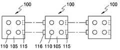
도 2a 및 도 2b를 참조하면, 본 발명의 바람직한 실시예에 따른 발광 어셈블리(120)는 조립 가능하게 된 복수 개의 발광 모듈(100)을 연결하여 원하는 사이즈로 구성될 수 있다. 발광 모듈(100)은 기판(105)에 복수의 발광 소자 유닛(110)이 배열되고, 상기 기판(105)에 발광 모듈들을 서로 전기적으로 결합할 수 있도록 전기 접속부(115)(116)가 구비된다. 상기 전기 접속부는 이웃하는 발광 모듈을 결합할 수 있도록 암수 결합될 수 있는 제1 접속부(115)와 제2 접속부(116)로 구성될 수 있다. 상기 발광 소자 유닛(110)의 개수는 도 2a에서는 4개로 구성된 경우를 예시하였으나 다양하게 구성될 수 있음은 물론이다.2A and 2B, the
상기 기판(105)은 PCB(Printed Circuit Board)일 수 있다. 기판(105)을 PCB로 제작하는 경우에는 별도의 PCB가 필요 없으므로 구조를 더욱 단순화할 수 있다. 한편, PCB를 별도로 마련하고, PCB 위에 상기 발광 모듈(100)을 결합하여 조립하는 것도 가능하다.The
상기 발광 모듈(100)은 디스플레이의 스크린의 사이즈에 따라 적당한 개수로 선택되어 상기 전기 접속부(115)를 통해 결합됨으로써 자유롭게 조립 가능하다.The
상기 발광 소자 유닛(110)은 적어도 두 개의 파장 범위의 광을 조사하는 복수 개의 발광 소자를 구비한 멀티칩 발광 소자 유닛으로 구성될 수 있다. 발광 소자는 예를 들어 발광 다이오드일 수 있다. 또한, 발광 소자 유닛은 상기 발광 소자 에서 조사되는 광을 전반사시키기 위한 캡을 구비하여, 발광 소자에서 조사된 서로 다른 파장의 광을 발광 소자 유닛 내부에서 수회에 걸쳐 전반사시킴으로써 혼합시킨다.The light
발광 소자 유닛은 다양한 구조로 패키징될 수 있으며, 도 3a, 도 3b 및 도 3c에 여러 가지 예가 도시되어 있다. 발광 소자 유닛(110)은 도 3a에 도시된 바와 같이 베이스(111)에 복수 개의 발광 소자(112)가 배열되어 있고, 복수 개의 발광 소자(112)의 상방에 캡(113)이 배치된다.The light emitting device unit may be packaged in various structures, and various examples are illustrated in FIGS. 3A, 3B, and 3C. In the light
상기 발광 소자(112)들은 적어도 두 개의 서로 다른 파장 범위의 광을 발광시키는 발광 소자들로 구성된다. 예를 들어, 상기 발광 소자(112)는 적색 파장 범위의 광을 발광시키는 제1 발광 소자(112a), 녹색 파장 범위의 광을 발광시키는 제2 발광 소자(112b), 청색 파장 범위의 광을 발광시키는 제3 발광 소자(112c)를 구비할 수 있다.The
도 3a에서는 8개의 발광 소자로 구성되며, 제1 발광 소자(112a)가 세 개, 제2 발광 소자(112b)가 두 개, 제3 발광 소자(112c)가 세 개로 구성된다. 각 파장 범위별 발광 소자의 개수 또는 배열 형태는 각 파장별 발광 소자로부터 출사되는 광량을 고려하여 원하는 색 온도 범위에 따라 적당하게 구성될 수 있다. 본 발명에서는 복수의 파장 범위의 광을 발광하는 발광 소자를 배열 방식, 배열 개수를 다양하게 구성하여 발광 소자 유닛으로 세팅할 수 있는 자유도가 크기 때문에 칼라 구현에 유리하며, 제조자의 입장에서도 칼라 선택도가 큰 이점이 있다. 또한, 본 발명에서와 같이 발광 소자 유닛을 멀티칩을 가지는 구조로 구성하여도 단일칩을 가지 는 발광 다이오드에 비해 그 크기가 크게 변하지 않으므로 부피 증가에 대한 염려는 없다.In FIG. 3A, eight light emitting devices are configured, three first
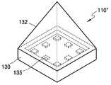
상기 발광 조사들에서 발광된 광은 상기 캡(113)을 통해 캡 내부에서 수회에 걸쳐 전반사되면서 서로 혼합된다. 상기 캡(113)은 인접한 외부 매질보다 큰 굴절률을 가지는 투명 재질로 형성되며, 예를 들어 렌즈로 구성될 수 있다. 또한, 상기 캡(113)은 원뿔형으로 구성되어 있지만, 다양한 형태의 캡으로 구성할 수 있다. 도 3b에 도시된 발광 소자 유닛(110')은 돔형 캡(114)을 구비하거나 또는 도 3c에 도시된 발광 소자 유닛(110")은 다각뿔형 캡 예를 들어, 사각뿔 캡(132)을 구비한다. 상기 발광 소자 유닛(110")은 사각 베이스(130)에 복수의 발광 소자(135)를 구비하고, 상기 베이스(130)의 상부에 사각뿔형 캡(132)을 구비한다.The light emitted from the light emitting irradiations are mixed with each other while totally reflecting inside the cap through the
발광 소자들(112)(135)은 베이스(111)(130)의 중심부에는 배치되지 않고 베이스(111)(130)의 주변부에 배치되는 것이 바람직하다. 발광 소자들을 베이스(111)(130)의 중심부에 배치하지 않음으로써 휘점이 발생되는 것을 방지할 수 있다. 휘점은 발광 소자에서 발광된 광이 균일하게 확산되지 못하여 상대적으로 밝은 휘도를 가지고 조사되어 부분적으로 밝은 점으로 보여지는 것으로 화질 저하의 한 요인이 된다. 발광 소자가 베이스(111)(130)의 중심부에 위치되고, 중심부에 위치된 발광 소자에서 광이 조사되면 그 대부분의 광은 상기 캡(113)(114)(132)의 꼭지점을 향해 입사되어 전반사 되지 않고 그대로 통과되어 나간다. 즉, 발광 소자가 캡(113)(114)(132)의 중심부에 대향되는 베이스의 중심부에 배치되면 그 발광 소자에서 발광되는 대부분의 광이 상기 캡(113)(114)(132)의 임계각보다 작은 각으로 입사되기 때문에 캡(113)(114)(132)을 통과해 직진하거나 굴절되어 나간다. 이에 반해, 발광 소자가 베이스(111)(130)의 주변부에 배치되면 발광 소자에서 발광된 광의 대부분이 캡(113)(114)(132)의 임계각보다 큰 각도로 입사되어 내부에서 전반사 된다.The
상기 발광 소자들(112)(135)에서 조사된 서로 다른 파장의 광들은 상기 캡(113)(114)(132)에서 수회 전반사 되면서 혼합된 후 캡 외부로 방출되기 때문에 칼라광 혼합을 위한 공간을 크게 줄일 수 있고 그럼으로써 디스플레이의 사이즈를 작게 할 수 있다.Since light of different wavelengths irradiated from the
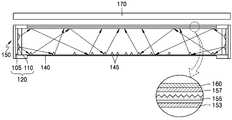
본 발명에 따른 디스플레이는 도 4에 도시된 바와 같이 백라이트 유닛(150)과, 백라이트 유닛(150)으로부터 조사된 광을 이용하여 영상을 형성하기 위한 디스플레이 패널(170)을 포함한다. 백라이트 유닛(150)은 발광 모듈(100)들로 조립된 발광 어셈블리(120)와, 상기 발광 어셈블리(120)로부터 조사된 광을 상기 디스플레이 패널(170)쪽으로 향하도록 안내하기 위한 도광판(140)을 구비한다.As shown in FIG. 4, the display according to the present invention includes a
상기 도광판(140)과 디스플레이 패널(170) 사이에는 광을 확산시키기 위한 확산판(153)과, 광의 진행 경로를 보정하기 위한 프리즘 시트(155)와, 상기 프리즘 시트(155)를 통과한 광을 디스플레이 패널을 향해 직진하도록 방향성을 향상시키는 밝기 향상 필름(BEF; Bright Enhancement Film)(157)이 배치된다. 상기 밝기 향상 필름(157)은 확산판(153)에서 나오는 광을 굴절 및 집광시켜서 광의 방향성을 향상시킴으로써 밝기를 크게 한다.Between the
상기 디스플레이 패널(170)은 예를 들어 액정 패널로 구성될 수 있다. 액정 패널을 이용하는 경우, 상기 밝기 향상 필름(157) 상부에 편광 효율을 향상시키기 위한 편광 향상 필름(160)을 더 구비할 수 있다. 상기 편광 향상 필름(160)은 예컨대 p편광의 광은 투과시키고, s편광의 광은 반사시키는 과정을 통해 입사된 광의 대부분이 일 편광 예컨대 p편광의 광으로 출사되도록 한다.The
상기 도광판(140)의 바닥면에 프리즘 패턴(145)이 형성될 수 있다. 상기 프리즘 패턴(145)은 상기 발광 어셈블리(120)로부터 조사된 광이 도광판(140)을 통해 반사될 때 발광 어셈블리(120)로부터 멀리 떨어질수록 광세기가 점점 감소되는 것을 방지하여 광의 균일도를 향상시킨다. 프리즘 패턴(145)은 발광 어셈블리(120)로부터 멀리 떨어질수록 조밀하게 배열된다. 또한, 발광 어셈블리(120)가 도광판(140)의 양측에 배치될 때, 프리즘 패턴(145)은 도광판(140)의 중심선을 기준으로 대칭적으로 배열되는 것이 좋다.The
상술한 바와 같이 본 발명에 따른 발광 어셈블리는 블록화된 발광 모듈을 이용하여 디스플레이의 사이즈에 따라 다양하게 조립 가능하므로 매우 유용하게 사용될 수 있다. 또한, 일반적으로 백라이트 유닛의 가장자리에서의 휘도가 상대적으로 낮은 것을 개선하기 위해 발광 어셈블리의 가장 자리에 위치된 발광 모듈에 공급되는 전류를 나머지 발광 모듈에 공급되는 전류보다 크게 할 수 있다. 이는 발광 모듈마다 독립적으로 전류 공급을 제어할 수 있기 때문에 가능하다.As described above, the light emitting assembly according to the present invention can be very useful because it can be variously assembled according to the size of the display using the blocked light emitting module. Also, in general, in order to improve that the luminance at the edge of the backlight unit is relatively low, the current supplied to the light emitting module positioned at the edge of the light emitting assembly may be larger than the current supplied to the remaining light emitting modules. This is possible because the current supply can be controlled independently for each light emitting module.
한편, 본 발명에 따른 발광 어셈블리는 가장자리 발광형 백라이트 유닛에 뿐만 아니라 직하형 백라이트 유닛에도 적용 가능하다.On the other hand, the light emitting assembly according to the present invention can be applied not only to the edge-emitting backlight unit but also to the direct backlight unit.
상기한 실시예들은 예시적인 것에 불과한 것으로, 당해 기술분야의 통상을 지식을 가진 자라면 이로부터 다양한 변형 및 균등한 타 실시예가 가능하다. 따라서, 본 발명의 진정한 기술적 보호범위는 하기의 특허청구범위에 기재된 발명의 기술적 사상에 의해 정해져야만 할 것이다.The above embodiments are merely exemplary, and various modifications and equivalent other embodiments are possible to those skilled in the art. Therefore, the true technical protection scope of the present invention will be defined by the technical spirit of the invention described in the claims below.
본 발명에 따른 발광 어셈블리는 독립적인 블록으로 구성된 발광 모듈을 이용하여 조립가능하므로 디스플레이의 사이즈에 관계없이 자유롭게 사용가능하며, 불량 소자가 발생한 경우 교체가 용이하다. 따라서, 디스플레이의 사이즈마다 백라이트 유닛에 사용되는 광원의 생산을 위해 각각 다른 생산라인을 구비할 필요가 없기 때문에 제조 비용을 크게 저감시킬 수 있다. 더 나아가, 발광 모듈을 독립적으로 구동가능하므로 발광 어셈블리의 가장 자리부에 위치된 발광 모듈의 전류를 다른 발광 모듈에 비해 상대적으로 크게 공급하여 가장자리에서 생기는 휘점 저하를 방지할 수 있다.Since the light emitting assembly according to the present invention can be assembled using a light emitting module composed of independent blocks, the light emitting assembly can be freely used regardless of the size of the display, and it is easy to replace the defective device. Therefore, the manufacturing cost can be greatly reduced because it is not necessary to have different production lines for the production of the light source used for the backlight unit for each size of the display. Furthermore, since the light emitting module can be driven independently, the current of the light emitting module positioned at the edge of the light emitting assembly can be supplied relatively larger than that of other light emitting modules, thereby preventing the bright point from occurring at the edge.
발광 어셈블리의 사이즈를 선택적으로 구성하여 백라이트 유닛 및 디스플레이에 폭넓게 적용할 수 있다.The size of the light emitting assembly may be selectively configured to be widely applied to the backlight unit and the display.
Claims (15)
Translated fromKoreanPriority Applications (4)
| Application Number | Priority Date | Filing Date | Title |
|---|---|---|---|
| KR1020050086242AKR100750130B1 (en) | 2005-03-23 | 2005-09-15 | Light emitting assembly, backlight unit and display |
| EP06111516AEP1705514B1 (en) | 2005-03-23 | 2006-03-21 | Light emitting assembly, backlight unit and display having the same |
| CNA2006100585985ACN1837922A (en) | 2005-03-23 | 2006-03-22 | Light-emitting assembly, backlight unit and display with the backlight unit |
| US11/386,785US7447416B2 (en) | 2005-03-23 | 2006-03-23 | Light emitting assembly, backlight unit and display having the same |
Applications Claiming Priority (3)
| Application Number | Priority Date | Filing Date | Title |
|---|---|---|---|
| US66419305P | 2005-03-23 | 2005-03-23 | |
| US60/664,193 | 2005-03-23 | ||
| KR1020050086242AKR100750130B1 (en) | 2005-03-23 | 2005-09-15 | Light emitting assembly, backlight unit and display |
Publications (2)
| Publication Number | Publication Date |
|---|---|
| KR20060102472A KR20060102472A (en) | 2006-09-27 |
| KR100750130B1true KR100750130B1 (en) | 2007-08-21 |
Family
ID=36587414
Family Applications (1)
| Application Number | Title | Priority Date | Filing Date |
|---|---|---|---|
| KR1020050086242AExpired - Fee RelatedKR100750130B1 (en) | 2005-03-23 | 2005-09-15 | Light emitting assembly, backlight unit and display |
Country Status (4)
| Country | Link |
|---|---|
| US (1) | US7447416B2 (en) |
| EP (1) | EP1705514B1 (en) |
| KR (1) | KR100750130B1 (en) |
| CN (1) | CN1837922A (en) |
Families Citing this family (18)
| Publication number | Priority date | Publication date | Assignee | Title |
|---|---|---|---|---|
| KR100705702B1 (en)* | 2005-10-24 | 2007-04-09 | 주식회사 나모텍 | Color mixing lens for display and backlight device equipped with the same |
| KR100786096B1 (en) | 2006-09-26 | 2007-12-21 | 엘지전자 주식회사 | Backlight Unit and Its Printed Circuit Board |
| CN101681059B (en)* | 2007-05-29 | 2014-03-05 | 皇家飞利浦电子股份有限公司 | Lighting systems, illuminators and backlight units |
| KR101498682B1 (en)* | 2008-08-20 | 2015-03-04 | 삼성전자주식회사 | Light emitting diode module |
| US8579473B2 (en)* | 2008-09-12 | 2013-11-12 | Koninklijke Philips N.V. | Luminaire for indirect illumination |
| TWI394916B (en)* | 2009-09-28 | 2013-05-01 | Hannstar Display Corp | Light emitting unit, backlight module and displaying device |
| TW201126764A (en)* | 2010-01-25 | 2011-08-01 | Icp Technology Co Ltd | Method for manufacturing light-emitting diode with substrate having fine perforations and light-emitting diode |
| KR20120023921A (en)* | 2010-09-03 | 2012-03-14 | 엘지이노텍 주식회사 | Backlight unit |
| KR20130046042A (en)* | 2011-10-27 | 2013-05-07 | 삼성전자주식회사 | Backlight unit and display apparatus having the same |
| US9395052B1 (en)* | 2012-11-13 | 2016-07-19 | Larry N. Shew | Modular lighting assembly |
| TW201422968A (en)* | 2012-12-11 | 2014-06-16 | Hon Hai Prec Ind Co Ltd | LED lamp |
| CN103016990B (en)* | 2012-12-21 | 2014-11-05 | 广东爱华新光电科技有限公司 | LED (Light Emitting Diode) lamp tube assembly |
| CN103900012A (en)* | 2014-04-17 | 2014-07-02 | 南宁桂格精工科技有限公司 | Daytime traveling crane lamp set capable of being combined at will |
| CN104048217A (en)* | 2014-06-24 | 2014-09-17 | 深圳市华星光电技术有限公司 | Direct-type backlight module and liquid crystal display device |
| CN104819430A (en)* | 2015-04-29 | 2015-08-05 | 武汉华星光电技术有限公司 | Tri-phosphor light emitting module, backlight module and liquid crystal display panel |
| EP3292347B1 (en)* | 2015-05-04 | 2018-12-19 | Philips Lighting Holding B.V. | Repeatable louver accessory for luminaires |
| EP3894741B1 (en)* | 2018-12-13 | 2023-02-15 | Lumileds LLC | Automotive headlight with dual correlated colour temperature |
| CN111885820B (en)* | 2020-08-07 | 2021-12-31 | 珠海格力电器股份有限公司 | Electric appliance, controller, control panel and panel unit thereof |
Citations (8)
| Publication number | Priority date | Publication date | Assignee | Title |
|---|---|---|---|---|
| JPH1039301A (en)* | 1996-07-24 | 1998-02-13 | Shichizun Denshi:Kk | Color display device |
| KR19990023425U (en)* | 1997-12-05 | 1999-07-05 | 손욱 | Optical module using light emitting diode |
| KR20010097147A (en)* | 2000-04-20 | 2001-11-08 | 박득일 | Back Light Unit by Use of White LED and Emission Method of White Light in High Purity |
| JP2001337626A (en)* | 2000-05-24 | 2001-12-07 | Avix Inc | Panel type LED display module |
| KR20020047534A (en)* | 2000-12-13 | 2002-06-22 | 구본준, 론 위라하디락사 | Backlight unit in Liquid crystal display |
| KR20050000647A (en)* | 2003-06-24 | 2005-01-06 | 엘지.필립스 엘시디 주식회사 | Liquid crystal display device using the light emitting diode |
| KR20060091640A (en)* | 2005-02-16 | 2006-08-21 | 삼성전자주식회사 | Multichip Light Emitting Diode Unit, Backlight Unit and Liquid Crystal Display Apparatus |
| KR20060095345A (en)* | 2005-02-28 | 2006-08-31 | 엘지.필립스 엘시디 주식회사 | Backlight Assembly and Liquid Crystal Display Using Same |
Family Cites Families (32)
| Publication number | Priority date | Publication date | Assignee | Title |
|---|---|---|---|---|
| JPS6184880A (en) | 1984-10-02 | 1986-04-30 | Sharp Corp | solid state light emitting display |
| US5822053A (en)* | 1995-04-25 | 1998-10-13 | Thrailkill; William | Machine vision light source with improved optical efficiency |
| KR100421900B1 (en) | 1997-04-09 | 2004-04-17 | 엘지.필립스 엘시디 주식회사 | back light of liquid grystal display device |
| JP2000068562A (en) | 1998-08-21 | 2000-03-03 | Stanley Electric Co Ltd | Led lamp |
| JP2000353405A (en)* | 1999-06-08 | 2000-12-19 | Shinichi Kobayashi | Lamp constituted of red, blue and green light emitting diode chips |
| WO2001008228A1 (en) | 1999-07-26 | 2001-02-01 | Labosphere Institute | Bulk lens, light emitting body, lighting device and optical information system |
| JP4352522B2 (en)* | 1999-09-01 | 2009-10-28 | ソニー株式会社 | Light-emitting flat display element |
| IT1315709B1 (en)* | 2000-06-09 | 2003-03-18 | Omnilux Srl | MODULAR LIGHTING ELEMENTS WITH LED DIODES. |
| KR20020041480A (en) | 2000-11-28 | 2002-06-03 | 유순재 | Back-light source module of liquid crystal display |
| DE10060653A1 (en)* | 2000-12-06 | 2002-06-20 | Epcos Ag | Electric double layer capacitor |
| US20020135298A1 (en)* | 2001-03-26 | 2002-09-26 | Pelka David G. | Light extractor apparatus |
| JP4674418B2 (en) | 2001-06-29 | 2011-04-20 | パナソニック株式会社 | Lighting equipment |
| JP4067802B2 (en)* | 2001-09-18 | 2008-03-26 | 松下電器産業株式会社 | Lighting device |
| JP4067801B2 (en)* | 2001-09-18 | 2008-03-26 | 松下電器産業株式会社 | Lighting device |
| US20030076034A1 (en)* | 2001-10-22 | 2003-04-24 | Marshall Thomas M. | Led chip package with four led chips and intergrated optics for collimating and mixing the light |
| JP3766042B2 (en) | 2002-06-21 | 2006-04-12 | 三菱電機株式会社 | Rear light source for display device and liquid crystal display device |
| CN2544172Y (en) | 2002-08-14 | 2003-04-09 | 崔淑萍 | Automatic color gradually changing multi-color lamp |
| TWI232281B (en)* | 2002-08-16 | 2005-05-11 | Toppoly Optoelectronics Corp | A backlight device of a LCD display |
| DE10242292A1 (en)* | 2002-09-12 | 2004-04-01 | Sebastian Matthias | Luminaire comprising LEDs in receptacle within frame, has frame with securing pieces for attaching and/or electrically connecting second luminaire |
| DE10245580B4 (en)* | 2002-09-27 | 2006-06-01 | Siemens Ag | Device for generating an image |
| GB0227632D0 (en) | 2002-11-27 | 2003-01-08 | Koninkl Philips Electronics Nv | Active matrix display |
| ATE412073T1 (en) | 2002-12-24 | 2008-11-15 | Chemetall Gmbh | METHOD FOR PRE-TREATMENT BEFORE COATING |
| JP4526807B2 (en) | 2002-12-24 | 2010-08-18 | 日本ペイント株式会社 | Pre-painting method |
| JP2004233809A (en) | 2003-01-31 | 2004-08-19 | Seiko Epson Corp | Surface light source unit, electro-optical device and electronic apparatus using the same |
| JP2004246117A (en) | 2003-02-14 | 2004-09-02 | Matsushita Electric Ind Co Ltd | Backlight device |
| JP4504662B2 (en)* | 2003-04-09 | 2010-07-14 | シチズン電子株式会社 | LED lamp |
| KR100508245B1 (en) | 2003-04-16 | 2005-08-17 | 엘지.필립스 엘시디 주식회사 | Liquid crystal module and driving apparatus and method thereof |
| KR20040096186A (en) | 2003-05-07 | 2004-11-16 | 엘지.필립스 엘시디 주식회사 | Back light unit and liquid crystal display device by using the same |
| US20040228127A1 (en) | 2003-05-16 | 2004-11-18 | Squicciarini John B. | LED clusters and related methods |
| US7394448B2 (en)* | 2003-06-20 | 2008-07-01 | Lg. Display Co., Ltd | Method and apparatus for driving liquid crystal display device |
| TWI244535B (en)* | 2004-03-24 | 2005-12-01 | Yuan Lin | A full color and flexible illuminating strap device |
| US7602369B2 (en)* | 2004-05-04 | 2009-10-13 | Sharp Laboratories Of America, Inc. | Liquid crystal display with colored backlight |
- 2005
- 2005-09-15KRKR1020050086242Apatent/KR100750130B1/ennot_activeExpired - Fee Related
- 2006
- 2006-03-21EPEP06111516Apatent/EP1705514B1/ennot_activeNot-in-force
- 2006-03-22CNCNA2006100585985Apatent/CN1837922A/enactivePending
- 2006-03-23USUS11/386,785patent/US7447416B2/ennot_activeExpired - Fee Related
Patent Citations (8)
| Publication number | Priority date | Publication date | Assignee | Title |
|---|---|---|---|---|
| JPH1039301A (en)* | 1996-07-24 | 1998-02-13 | Shichizun Denshi:Kk | Color display device |
| KR19990023425U (en)* | 1997-12-05 | 1999-07-05 | 손욱 | Optical module using light emitting diode |
| KR20010097147A (en)* | 2000-04-20 | 2001-11-08 | 박득일 | Back Light Unit by Use of White LED and Emission Method of White Light in High Purity |
| JP2001337626A (en)* | 2000-05-24 | 2001-12-07 | Avix Inc | Panel type LED display module |
| KR20020047534A (en)* | 2000-12-13 | 2002-06-22 | 구본준, 론 위라하디락사 | Backlight unit in Liquid crystal display |
| KR20050000647A (en)* | 2003-06-24 | 2005-01-06 | 엘지.필립스 엘시디 주식회사 | Liquid crystal display device using the light emitting diode |
| KR20060091640A (en)* | 2005-02-16 | 2006-08-21 | 삼성전자주식회사 | Multichip Light Emitting Diode Unit, Backlight Unit and Liquid Crystal Display Apparatus |
| KR20060095345A (en)* | 2005-02-28 | 2006-08-31 | 엘지.필립스 엘시디 주식회사 | Backlight Assembly and Liquid Crystal Display Using Same |
Also Published As
| Publication number | Publication date |
|---|---|
| US7447416B2 (en) | 2008-11-04 |
| EP1705514A1 (en) | 2006-09-27 |
| US20060215405A1 (en) | 2006-09-28 |
| KR20060102472A (en) | 2006-09-27 |
| CN1837922A (en) | 2006-09-27 |
| EP1705514B1 (en) | 2012-02-08 |
Similar Documents
| Publication | Publication Date | Title |
|---|---|---|
| US7447416B2 (en) | Light emitting assembly, backlight unit and display having the same | |
| KR100619069B1 (en) | Multichip Light Emitting Diode Unit, Backlight Unit and Liquid Crystal Display Apparatus | |
| US7210839B2 (en) | Backlight system and liquid crystal display employing the same | |
| JP4589361B2 (en) | Light source cube, flat light source unit and liquid crystal display device using the same | |
| JP5066572B2 (en) | Backlight unit and liquid crystal display device including the same | |
| KR100764377B1 (en) | Edge type backlight unit | |
| JP5999983B2 (en) | Illumination device and display device | |
| KR20060107923A (en) | Luminous panel and display system | |
| JP2012216747A (en) | Light-emitting device, lighting device and display | |
| JP2004342587A (en) | Backlight and liquid crystal display device using the same | |
| WO2011004637A1 (en) | Illumination device, display device, and television receiver | |
| KR101339768B1 (en) | Plane light source and lcd backlight unit comprising the same | |
| US8210700B2 (en) | Backlight module | |
| US20060203484A1 (en) | Light emitting diode, light emitting diode module, and related backlight system | |
| KR20190021522A (en) | Light guide plate and backlight unit having the same | |
| JP5386551B2 (en) | Light emitting device, display device, and reflecting member design method | |
| KR101294849B1 (en) | Backlight assemlby | |
| JP2013247092A (en) | Light-emitting device, lighting device, and display device | |
| KR101042698B1 (en) | Surface light source device | |
| WO2011074410A1 (en) | Illuminating device, display device, and television receiver | |
| KR100664373B1 (en) | Backlit panel with white light emitting diode | |
| KR102391395B1 (en) | Optical lens and backlight unit including the same and Liquid crystal display device | |
| KR101266709B1 (en) | Backlight unit and liquid crystal display device using the same | |
| KR20130004661A (en) | Light source module, backlight unit, display apparatus, television set and illumination apparatus | |
| CN216647038U (en) | Light-emitting device, backlight module and display panel |
Legal Events
| Date | Code | Title | Description |
|---|---|---|---|
| A201 | Request for examination | ||
| PA0109 | Patent application | St.27 status event code:A-0-1-A10-A12-nap-PA0109 | |
| PA0201 | Request for examination | St.27 status event code:A-1-2-D10-D11-exm-PA0201 | |
| D13-X000 | Search requested | St.27 status event code:A-1-2-D10-D13-srh-X000 | |
| PG1501 | Laying open of application | St.27 status event code:A-1-1-Q10-Q12-nap-PG1501 | |
| D14-X000 | Search report completed | St.27 status event code:A-1-2-D10-D14-srh-X000 | |
| E902 | Notification of reason for refusal | ||
| PE0902 | Notice of grounds for rejection | St.27 status event code:A-1-2-D10-D21-exm-PE0902 | |
| AMND | Amendment | ||
| P11-X000 | Amendment of application requested | St.27 status event code:A-2-2-P10-P11-nap-X000 | |
| P13-X000 | Application amended | St.27 status event code:A-2-2-P10-P13-nap-X000 | |
| E601 | Decision to refuse application | ||
| PE0601 | Decision on rejection of patent | St.27 status event code:N-2-6-B10-B15-exm-PE0601 | |
| J201 | Request for trial against refusal decision | ||
| PJ0201 | Trial against decision of rejection | St.27 status event code:A-3-3-V10-V11-apl-PJ0201 | |
| AMND | Amendment | ||
| E13-X000 | Pre-grant limitation requested | St.27 status event code:A-2-3-E10-E13-lim-X000 | |
| P11-X000 | Amendment of application requested | St.27 status event code:A-2-2-P10-P11-nap-X000 | |
| P13-X000 | Application amended | St.27 status event code:A-2-2-P10-P13-nap-X000 | |
| PB0901 | Examination by re-examination before a trial | St.27 status event code:A-6-3-E10-E12-rex-PB0901 | |
| B701 | Decision to grant | ||
| PB0701 | Decision of registration after re-examination before a trial | St.27 status event code:A-3-4-F10-F13-rex-PB0701 | |
| GRNT | Written decision to grant | ||
| PR0701 | Registration of establishment | St.27 status event code:A-2-4-F10-F11-exm-PR0701 | |
| PR1002 | Payment of registration fee | St.27 status event code:A-2-2-U10-U11-oth-PR1002 Fee payment year number:1 | |
| PG1601 | Publication of registration | St.27 status event code:A-4-4-Q10-Q13-nap-PG1601 | |
| G170 | Re-publication after modification of scope of protection [patent] | ||
| PG1701 | Publication of correction | St.27 status event code:A-5-5-P10-P19-oth-PG1701 Patent document republication publication date:20080418 Republication note text:Request for Correction Notice (Document Request) Gazette number:1007501300000 Gazette reference publication date:20070821 | |
| PR1001 | Payment of annual fee | St.27 status event code:A-4-4-U10-U11-oth-PR1001 Fee payment year number:4 | |
| PR1001 | Payment of annual fee | St.27 status event code:A-4-4-U10-U11-oth-PR1001 Fee payment year number:5 | |
| R18-X000 | Changes to party contact information recorded | St.27 status event code:A-5-5-R10-R18-oth-X000 | |
| FPAY | Annual fee payment | Payment date:20120730 Year of fee payment:6 | |
| PR1001 | Payment of annual fee | St.27 status event code:A-4-4-U10-U11-oth-PR1001 Fee payment year number:6 | |
| FPAY | Annual fee payment | Payment date:20130730 Year of fee payment:7 | |
| PR1001 | Payment of annual fee | St.27 status event code:A-4-4-U10-U11-oth-PR1001 Fee payment year number:7 | |
| FPAY | Annual fee payment | Payment date:20140730 Year of fee payment:8 | |
| PR1001 | Payment of annual fee | St.27 status event code:A-4-4-U10-U11-oth-PR1001 Fee payment year number:8 | |
| LAPS | Lapse due to unpaid annual fee | ||
| PC1903 | Unpaid annual fee | St.27 status event code:A-4-4-U10-U13-oth-PC1903 Not in force date:20150811 Payment event data comment text:Termination Category : DEFAULT_OF_REGISTRATION_FEE | |
| PC1903 | Unpaid annual fee | St.27 status event code:N-4-6-H10-H13-oth-PC1903 Ip right cessation event data comment text:Termination Category : DEFAULT_OF_REGISTRATION_FEE Not in force date:20150811 |