KR100749870B1 - Doherty power amplifier - Google Patents
Doherty power amplifierDownload PDFInfo
- Publication number
- KR100749870B1 KR100749870B1KR1020060050788AKR20060050788AKR100749870B1KR 100749870 B1KR100749870 B1KR 100749870B1KR 1020060050788 AKR1020060050788 AKR 1020060050788AKR 20060050788 AKR20060050788 AKR 20060050788AKR 100749870 B1KR100749870 B1KR 100749870B1
- Authority
- KR
- South Korea
- Prior art keywords
- amplifier
- input
- impedance
- carrier
- doherty
- Prior art date
- Legal status (The legal status is an assumption and is not a legal conclusion. Google has not performed a legal analysis and makes no representation as to the accuracy of the status listed.)
- Active
Links
- 230000003321amplificationEffects0.000claimsabstractdescription67
- 238000003199nucleic acid amplification methodMethods0.000claimsabstractdescription67
- 238000000034methodMethods0.000claimsabstractdescription46
- 239000000969carrierSubstances0.000claimsdescription2
- 239000003990capacitorSubstances0.000claims3
- 230000001276controlling effectEffects0.000claims1
- 230000001105regulatory effectEffects0.000claims1
- 238000010586diagramMethods0.000description10
- 230000000694effectsEffects0.000description2
- 230000010354integrationEffects0.000description2
- 238000010295mobile communicationMethods0.000description2
- 230000007423decreaseEffects0.000description1
- 238000005516engineering processMethods0.000description1
Images


Classifications
- H—ELECTRICITY
- H03—ELECTRONIC CIRCUITRY
- H03F—AMPLIFIERS
- H03F1/00—Details of amplifiers with only discharge tubes, only semiconductor devices or only unspecified devices as amplifying elements
- H03F1/02—Modifications of amplifiers to raise the efficiency, e.g. gliding Class A stages, use of an auxiliary oscillation
- H03F1/04—Modifications of amplifiers to raise the efficiency, e.g. gliding Class A stages, use of an auxiliary oscillation in discharge-tube amplifiers
- H03F1/06—Modifications of amplifiers to raise the efficiency, e.g. gliding Class A stages, use of an auxiliary oscillation in discharge-tube amplifiers to raise the efficiency of amplifying modulated radio frequency waves; to raise the efficiency of amplifiers acting also as modulators
- H03F1/07—Doherty-type amplifiers
- H—ELECTRICITY
- H03—ELECTRONIC CIRCUITRY
- H03F—AMPLIFIERS
- H03F3/00—Amplifiers with only discharge tubes or only semiconductor devices as amplifying elements
- H03F3/60—Amplifiers in which coupling networks have distributed constants, e.g. with waveguide resonators
- H03F3/602—Combinations of several amplifiers
- H—ELECTRICITY
- H03—ELECTRONIC CIRCUITRY
- H03F—AMPLIFIERS
- H03F1/00—Details of amplifiers with only discharge tubes, only semiconductor devices or only unspecified devices as amplifying elements
- H03F1/02—Modifications of amplifiers to raise the efficiency, e.g. gliding Class A stages, use of an auxiliary oscillation
- H03F1/0205—Modifications of amplifiers to raise the efficiency, e.g. gliding Class A stages, use of an auxiliary oscillation in transistor amplifiers
- H03F1/0288—Modifications of amplifiers to raise the efficiency, e.g. gliding Class A stages, use of an auxiliary oscillation in transistor amplifiers using a main and one or several auxiliary peaking amplifiers whereby the load is connected to the main amplifier using an impedance inverter, e.g. Doherty amplifiers
- H—ELECTRICITY
- H03—ELECTRONIC CIRCUITRY
- H03F—AMPLIFIERS
- H03F3/00—Amplifiers with only discharge tubes or only semiconductor devices as amplifying elements
- H03F3/189—High-frequency amplifiers, e.g. radio frequency amplifiers
- H03F3/19—High-frequency amplifiers, e.g. radio frequency amplifiers with semiconductor devices only
- H03F3/195—High-frequency amplifiers, e.g. radio frequency amplifiers with semiconductor devices only in integrated circuits
- H—ELECTRICITY
- H03—ELECTRONIC CIRCUITRY
- H03F—AMPLIFIERS
- H03F2200/00—Indexing scheme relating to amplifiers
- H03F2200/255—Amplifier input adaptation especially for transmission line coupling purposes, e.g. impedance adaptation
- H—ELECTRICITY
- H03—ELECTRONIC CIRCUITRY
- H03F—AMPLIFIERS
- H03F2200/00—Indexing scheme relating to amplifiers
- H03F2200/423—Amplifier output adaptation especially for transmission line coupling purposes, e.g. impedance adaptation
- H—ELECTRICITY
- H03—ELECTRONIC CIRCUITRY
- H03F—AMPLIFIERS
- H03F2200/00—Indexing scheme relating to amplifiers
- H03F2200/451—Indexing scheme relating to amplifiers the amplifier being a radio frequency amplifier
Landscapes
- Engineering & Computer Science (AREA)
- Power Engineering (AREA)
- Microelectronics & Electronic Packaging (AREA)
- Amplifiers (AREA)
Abstract
Translated fromKoreanDescription
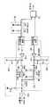
Translated fromKorean도 1은 π-네트워크로 쿼터 웨이브 트랜스포머(quarter wave transformer)를 구현한 종래 기술의 도허티 전력 증폭 장치의 회로도,1 is a circuit diagram of a prior art Doherty power amplification apparatus implementing a quarter wave transformer with a π-network.
도 2는 본 발명의 제 1 실시 예에 따라 새로운 출력 정합 방법이 적용된 도허티 전력 증폭 장치의 회로도,2 is a circuit diagram of a Doherty power amplification apparatus to which a new output matching method is applied according to a first embodiment of the present invention;
도 3은 본 발명의 제 2 실시 예에 따라 새로운 입력 정합 방법이 적용된 도허티 전력 증폭 장치의 회로도,3 is a circuit diagram of a Doherty power amplification apparatus to which a new input matching method is applied according to a second embodiment of the present invention;
도 4a는 본 발명에 의한 도허티 전력 증폭 장치의 전력 분배 그래프,Figure 4a is a power distribution graph of the Doherty power amplification apparatus according to the present invention,
도 4b는 출력 전력 대비 효율 그래프를 Class AB와 비교해서 나타낸 그래프,Figure 4b is a graph showing the efficiency graph compared to the output power, Class AB,
도 4c는 높은 효율을 위해 새로운 전력 분배 방식을 구현한 도허티 전력 증폭 장치의 입력 정합 회로의 개념을 설명한 구성도,4c is a block diagram illustrating the concept of an input matching circuit of a Doherty power amplification device implementing a new power distribution scheme for high efficiency;
도 5는 본 발명의 제 3 실시 예에 따라 새로운 입력 정합 방법과 출력 정합 방법을 함께 적용한 도허티 전력 증폭 장치의 회로도,5 is a circuit diagram of a Doherty power amplification apparatus using a new input matching method and an output matching method according to a third embodiment of the present invention;
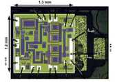
도 6은 본 발명의 내용을 토대로, 5GHz WLAN 응용을 위해 제작된 완전 집적된 도허티 전력 증폭기의 MMIC 전체 칩 사진.6 is a MMIC full chip photograph of a fully integrated Doherty power amplifier constructed for 5 GHz WLAN applications, based on the teachings of the present invention.
본 발명은 도허티 전력 증폭 장치에 관한 것으로, 더욱 상세하게는 도허티 전력 증폭 장치를 소형화해서 칩에 완전 집적화를 가능케 하기 위한 것이다.The present invention relates to a Doherty power amplification device, and more particularly, to miniaturize a Doherty power amplification device to enable full integration on a chip.
최근 이동통신 단말기, 중계기 및 기지국의 소형화 및 다기능화로 인해 배터리 타임을 늘리기 위한 노력으로서 전력 소모의 대부분을 차지하는 RF 전력 증폭 장치의 효율을 높이는 것에 대한 많은 연구가 이루어지고 있으며, 이 중에서 전력 증폭 장치의 효율을 높이기 위한 대표적인 방법 중의 하나인 도허티 전력 증폭 장치에 대한 연구가 많이 이루어지고 있다.Recently, many efforts have been made to increase the efficiency of the RF power amplification device, which takes up most of the power consumption in an effort to increase battery time due to the miniaturization and multifunctionalization of mobile communication terminals, repeaters, and base stations. There is a lot of research on the Doherty power amplification device, which is one of the representative methods for improving efficiency.
도허티 증폭 장치는 1936년에 W.H. Doherty에 의해서 처음 제안되었는데, 쿼터 웨이브 트랜스포머(quarter wave transformer)(λ/4 라인)를 사용해서 캐리어 증폭기와 피킹 증폭기를 병렬로 연결하는 방식으로 전력 레벨에 따라 피킹 증폭기가 로드에 공급하는 전류의 양을 달라지게 함으로써 캐리어 증폭기의 로드 라인 임피던스를 조절하여 효율을 높이는 장치이다.Doherty amplification unit was established in 1936 by W.H. Originally proposed by Doherty, the amount of current supplied to a load by the peaking amplifier, depending on the power level, by using a quarter-wave transformer (λ / 4 line) to connect the carrier amplifier and the peaking amplifier in parallel. It is a device to increase the efficiency by adjusting the load line impedance of the carrier amplifier by varying.
한편, 이동 통신용 도허티 증폭 장치를 구현하는데 있어서는 크기의 제한이 점점 중요해지고 있으며, 소형화로 계속 발전되고 있는 추세이나, 도허티 증폭 장치를 구현하는데 있어 기존의 도허티 구성 방법으로는 칩과 패키지의 크기와 이에 따른 가격 상승의 문제를 가지고 있다. 대표적으로 원인이 되고 있는 항목으로는, 도허티 증폭 장치를 구성하는데 있어 필요한 캐리어 증폭기의 로드 라인 임피던스를 조절시켜주기 위한 쿼터 웨이브 트랜스포머와 입력 전력 분배 목적인 3dB 90ㅀ하이브리드 분배기를 들 수 있다.On the other hand, the limitation of the size is increasingly important in the implementation of the Doherty amplification device for mobile communication, and the trend continues to develop into miniaturization, the existing Doherty amplification method in the implementation of the Doherty amplification device is the size and size of the chip and package It has a problem of price increase. Representative factors include a quarter-wave transformer for adjusting the load line impedance of the carrier amplifier required for constructing the Doherty amplifier, and a 3dB 90kHz hybrid divider for input power distribution purposes.
종래 기술에 의한 도허티 전력 증폭 장치에서는 도 1에 도시된 바와 같이 쿼터 웨이브 트랜스포머(quarter wave transformer)를 L과 C로 구성한 λ/4 π-네트워크(50)로 대체하고 있다.In the prior art Doherty power amplification apparatus, a quarter wave transformer is replaced with a λ / 4 π-
캐리어 증폭기(30) 및 피킹 증폭기(35)의 전단에 각각 입력 정합 회로(20, 25)를 연결하며, 캐리어 증폭기(30)와 피킹 증폭기(35)의 출력단에 각각 출력 정합 회로(40, 45)를 연결한다.
또한, 입력 전력 분배 목적인 3dB 90ㅀ하이브리드 분배기는 소형화 및 집적화 목적을 위해 사용하지 않았으며, 캐리어 증폭기(30)와 피킹 증폭기(35)간의 입력은 접합된 상태로 그냥 두며, 캐리어 증폭기(30)와 피킹 증폭기(35)간의 지연(delay)을 맞춰주기 위해 피킹 증폭기(35)의 입력단에 쿼터 웨이브 트랜스포머 역할을 하는 λ/4 π-네트워크를 제 1 지연 회로(55)로 추가하였다. 도면 중 미설명 부호인 10은 전력 스플리터(power splitter)이다.In addition, the 3dB 90kHz hybrid divider, which is an input power distribution purpose, was not used for miniaturization and integration purposes, and the input between the
아울러, 또 다른 미설명 부호인 60은 오프셋 라인이다. 오프셋 라인(60)은 피킹 증폭기(35) 쪽으로의 아웃풋 임피던스를 무한대로 보내는 기능을 하여 낮은 전력레벨에서 캐리어 증폭기(30)의 출력이 로드쪽이 아닌 피킹 증폭기(35) 쪽으로 새는 누수 전력을 막는다. 이때 오프셋 라인(60)이 ∠θP일 경우에 피킹 증폭기(35)의 입력단에는 제 1 지연 회로(55)가 λ/4-∠θP π-네트워크로 배치된다.In addition, another
그러나, 전술한 바와 같은 종래의 도허티 전력 증폭 장치는, 칩에 집적시키기에는 크기와 인덕터 손실로 인한 어려움이 있어서 PCB 패키지 상에서 구현하고 있는 실정이며, 이 역시 패키지 크기가 커지는 점과 여러 개의 수동 소자의 사용으로 인한 증폭 장치의 단가를 높이는 단점을 가지고 있다.However, the conventional Doherty power amplification device as described above has been implemented on a PCB package because of the difficulty in size and inductor loss to integrate into a chip, which also increases the package size and the number of passive components. It has the disadvantage of increasing the cost of the amplification device due to use.
또한 입력 전력 분배 목적인 3dB 90ㅀ하이브리드 분배기 사용에 따른 문제점을 해결하기 위하여 스위치를 이용해 도허티 구조를 바이패스 타입으로 전향하거나 능동 위상 분배기의 사용과 같은 여러 가지 노력이 이루어지고 있다. 하지만 이런 노력 역시 확실한 해결책이 되지는 못한 실정이며, 최근에 기지국 도허티 전력 증폭 장치 분야에서 제안된 이상적인 도허티 동작을 위해서는 높은 전력 레벨에서 캐리어/피킹 증폭기에 각각 3dB씩 나눠져서는 안되며, 피킹 증폭기 쪽으로 캐리어 증폭기에 비해 좀더 많은 입력 전력이 인가되어야 한다는 또 다른 문제점에는 여전히 한계를 가진다.In order to solve the problem of using a 3dB 90 ㅀ hybrid divider for input power distribution, various efforts have been made such as using a switch to convert the Doherty structure to the bypass type or using an active phase divider. However, this effort is also not a clear solution, and for the ideal Doherty operation recently proposed in the base station Doherty power amplification device, it should not be divided into 3 dB each of the carrier / peaking amplifier at a high power level, but rather into the picking amplifier. There is still a limit to another problem that more input power must be applied compared to the above.
본 발명은 이와 같은 종래의 문제점을 해결하기 위하여 제안한 것으로, 새로운 출력 정합 방법과 입력 정합 방법을 제공함으로써, 효율과 선형성 측면에서 큰 장점을 가진 도허티 전력 증폭 장치를 소형화 및 집적화 하는 데에 그 목적이 있다.The present invention has been proposed to solve such a conventional problem, and by providing a new output matching method and an input matching method, an object thereof is to miniaturize and integrate a Doherty power amplification device having great advantages in terms of efficiency and linearity. have.
본 발명의 다른 목적은 도허티 전력 증폭 장치에 새로운 입력 전력 분배 방법을 적용하여 좀더 이상적인 도허티 동작이 일어나게 하는데 있다.Another object of the present invention is to apply a new input power distribution method to the Doherty power amplification apparatus to make a more ideal Doherty operation.
이와 같은 목적들을 실현하기 위한 본 발명의 제 1 관점으로서 도허티 전력 증폭 장치는, 병렬로 연결한 캐리어 증폭기와 피킹 증폭기가 도허티 동작이 일어나게 하는 도허티 전력 증폭 장치로서, 캐리어 증폭기와 피킹 증폭기의 입력단에 각 각 연결된 복수의 입력 정합 회로와, 캐리어 증폭기의 출력단에 연결되어 캐리어 증폭기의 로드 라인 임피던스를 조절하는 임피던스 조절 회로와, 임피던스 조절 회로와 피킹 증폭기의 후단에 연결된 출력 정합 회로와, 피킹 증폭기의 입력단에 연결된 입력 정합 회로의 전단에 연결되어 캐리어 증폭기와 피킹 증폭기 사이의 지연을 맞춰주는 제 1 지연 회로를 포함한다.As a first aspect of the present invention for realizing the above objects, a Doherty power amplifying apparatus is a Doherty power amplifying apparatus in which a Doherty operation is performed by a carrier amplifier and a picking amplifier connected in parallel, each of which is connected to an input terminal of the carrier amplifier and the picking amplifier. A plurality of connected input matching circuits, an impedance adjusting circuit connected to an output terminal of the carrier amplifier to adjust a load line impedance of the carrier amplifier, an output matching circuit connected to an impedance adjusting circuit and a rear end of the peaking amplifier, and an input terminal of the peaking amplifier. And a first delay circuit coupled to the front end of the connected input matching circuit to adjust the delay between the carrier amplifier and the peaking amplifier.
본 발명의 제 2 관점으로서 도허티 전력 증폭 장치는, 병렬로 연결한 캐리어 증폭기와 피킹 증폭기가 도허티 동작이 일어나게 하는 도허티 전력 증폭 장치로서, 캐리어 증폭기와 피킹 증폭기의 출력단에 각각 연결된 복수의 출력 정합 회로와, 캐리어 증폭기의 출력단에 연결된 출력 정합 회로의 후단에 연결되어 캐리어 증폭기의 로드 라인 임피던스를 조절하는 임피던스 조절 회로와, 캐리어 증폭기와 피킹 증폭기의 입력단에 각각 연결된 복수의 입력 정합 회로와, 피킹 증폭기의 입력단에 연결된 입력 정합 회로의 전단에 연결되어 입력 전력레벨이 높아질 때에 캐리어 증폭기 쪽보다 피킹 증폭기로 쪽으로 더 많은 전력을 공급하는 전력 분배 회로와, 캐리어 증폭기의 입력단에 연결된 입력 정합 회로의 전단에 연결되어 전체적인 지연을 맞춰주는 제 2 지연 회로를 포함한다.As a second aspect of the present invention, a Doherty power amplifying apparatus includes a plurality of output matching circuits connected to an output terminal of a carrier amplifier and a peaking amplifier, wherein the Doherty power amplifying apparatus performs a Doherty operation between a carrier amplifier and a peaking amplifier connected in parallel. An impedance adjusting circuit connected to a rear end of an output matching circuit connected to an output terminal of the carrier amplifier to adjust a load line impedance of the carrier amplifier, a plurality of input matching circuits respectively connected to the input terminals of the carrier amplifier and the peaking amplifier, and an input terminal of the peaking amplifier A power distribution circuit connected to the front end of the input matching circuit, which supplies more power to the picking amplifier than the carrier amplifier side when the input power level is increased, and to the front end of the input matching circuit connected to the input of the carrier amplifier. To meet the
본 발명의 제 3 관점으로서 도허티 전력 증폭 장치는, 병렬로 연결한 캐리어 증폭기와 피킹 증폭기가 도허티 동작이 일어나게 하는 도허티 전력 증폭 장치로서, 캐리어 증폭기와 피킹 증폭기의 입력단에 각각 연결된 복수의 입력 정합 회로와, 캐리어 증폭기의 출력단에 연결되어 캐리어 증폭기의 로드 라인 임피던스를 조절하는 임피던스 조절 회로와, 임피던스 조절 회로와 피킹 증폭기의 후단에 연결된 출 력 정합 회로와, 피킹 증폭기의 입력단에 연결된 입력 정합 회로의 전단에 연결되어 입력 전력레벨이 높아질 때에 캐리어 증폭기 쪽보다 피킹 증폭기로 쪽으로 더 많은 전력을 공급하는 전력 분배 회로와, 캐리어 증폭기의 입력단에 연결된 입력 정합 회로의 전단에 연결되어 전체적인 지연을 맞춰주는 제 2 지연 회로를 포함한다.As a third aspect of the present invention, a Doherty power amplifying apparatus includes a plurality of input matching circuits connected to input terminals of a carrier amplifier and a peaking amplifier, wherein the Doherty power amplifying apparatus causes the Doherty operation to occur in parallel between a carrier amplifier and a peaking amplifier connected in parallel. An impedance control circuit connected to the output of the carrier amplifier to adjust the load line impedance of the carrier amplifier, an output matching circuit connected to the impedance control circuit and the rear end of the peaking amplifier, and an input matching circuit connected to the input of the peaking amplifier. Connected to supply more power to the picking amplifier than to the carrier amplifier when the input power level is high, and a second delay circuit connected to the front of the input matching circuit connected to the input of the carrier amplifier to match the overall delay. It includes.
이하, 본 발명의 바람직한 실시 예를 첨부된 도면들을 참조하여 상세히 설명한다. 아울러 본 발명을 설명함에 있어, 관련된 공지 구성 또는 기능에 대한 구체적인 설명이 본 발명의 요지를 흐릴 수 있다고 판단되는 경우에는 그 상세한 설명을 생략한다.Hereinafter, exemplary embodiments of the present invention will be described in detail with reference to the accompanying drawings. In addition, in describing the present invention, when it is determined that the detailed description of the related known configuration or function may obscure the gist of the present invention, the detailed description thereof will be omitted.
도 2는 본 발명의 제 1 실시 예에 따라 새로운 출력 정합 방법이 적용된 도허티 전력 증폭 장치의 회로도로서, 도 1과 비교할 때에 동일한 구성요소에 대해서는 동일한 참조부호를 명기하였다.FIG. 2 is a circuit diagram of a Doherty power amplifying apparatus to which a new output matching method is applied according to the first embodiment of the present invention, and the same reference numerals are designated for the same components when compared to FIG.
도허티 전력 증폭 장치에서 캐리어 증폭기의 로드 라인 임피던스를 조절하기 위한 쿼터 웨이브 트랜스포머를 도 1의 종래 기술처럼 L과 C로 구성된 λ/4 π-네트워크로 구성할 경우에 칩의 크기나 수동소자의 손실로 인해 문제가 발생하는데, 이때 중요시되는 부분이 인덕턴스 값이다. 도 1에 도시된 종래의 도허티 전력 증폭 장치에 의하면 캐리어 증폭기 출력단의 쿼터 웨이브 트랜스포머의 특성 임피던스가 100옴이 된다. 이때 여기에 상응하는 인덕터 값은 L = Z0/ω0에 의해 정해지는데, 이를 통해 알 수 있듯이 특성 임피던스가 낮을수록 작은 값의 인덕터로 구현할 수 있다.In the Doherty power amplification device, when the quarter wave transformer for adjusting the load line impedance of the carrier amplifier is configured as a λ / 4 π-network composed of L and C as in the prior art of FIG. The problem arises, where the important part is the inductance value. According to the conventional Doherty power amplifier shown in FIG. 1, the characteristic impedance of the quarter-wave transformer at the output stage of the carrier amplifier is 100 ohms. At this time, the corresponding inductor value is determined by L = Z0 / ω0. As can be seen, the lower the characteristic impedance, the smaller the inductor.
따라서, 쿼터 웨이브 트랜스포머의 특성 임피던스 값을 원하는 Ropt값으로 정하고, 이를 위해서 50옴 로드 저항의 값으로부터 먼저 Ropt/2 임피던스로 정합을 시켜온다. 이렇게 되면 캐리어 증폭기의 쿼터 웨이브 트랜스포머의 특성 임피던스는 기존의 100옴에서 Ropt로 낮아지는데, 물론 출력 전력 수준에 따라 다르지만 보통 Ropt는 10옴 이하의 값을 가지게 되고, 출력 전력 수준이 높아질수록 이 값은 작아지게 된다. 이로써, 캐리어 증폭기의 쿼터 웨이브 트랜스포머를 위해 필요한 인덕터 값을 기존 정합방법에 비해서 10배 이상 줄일 수 있다. 또한 이런 정합 방법은 기존의 정합 방법에서 캐리어 및 피킹 증폭기에 각각 쓰여진 출력 정합 회로를 하나로 쓸 수 있을 뿐만 이 하나의 정합 회로를 구성하는 수동소자인 인덕터를 본딩 인덕터로 대체 시킬 수 있어 캐리어 증폭기와 피킹 증폭기로 구성되는 주 증폭기의 출력 정합회로에 쓰여지는 수동소자의 수를 절반 이하로 줄일 수 있다. 이는 도허티 전력 증폭 장치의 칩 크기와 수동소자로 인해 발생되는 손실을 줄 일 수 있는 이점을 나타낸다.Therefore, the characteristic impedance value of the quarter wave transformer is set to the desired Ropt value, and for this purpose, the Ropt / 2 impedance is first matched from the value of the 50 ohm load resistance. The characteristic impedance of the quarter-wave transformer of the carrier amplifier is then lowered to Ropt at 100 ohms, which, of course, depends on the output power level, but usually Ropt is less than 10 ohms. The value becomes smaller. As a result, the inductor required for the quarter-wave transformer of the carrier amplifier can be reduced by more than 10 times compared to the conventional matching method. In addition, this matching method can use one output matching circuit written in the carrier and the peaking amplifier in the conventional matching method, and can replace the inductor, which is a passive element constituting the matching circuit, with the bonding inductor, so that the carrier amplifier and the peaking can be used. The number of passive elements used in the output matching circuit of the main amplifier consisting of the amplifier can be reduced to less than half. This has the advantage of reducing the losses caused by the chip size and passive components of the Doherty power amplifier.
도 2의 회로도에 나타낸 바와 같이 본 발명에 의한 출력 정합 방법을 이용한 도허티 전력 증폭 장치는 앞서 설명 한 바와 같이, 정합 및 도허티를 구성하기 위한 수동소자의 개수를 많이 줄일 수가 있게 되었고, 모든 수동소자는 모두 MMIC 칩에 집적이 가능하게 되었다.As shown in the circuit diagram of FIG. 2, the Doherty power amplification apparatus using the output matching method according to the present invention can reduce the number of passive elements for configuring the match and Doherty as described above. All have been integrated into MMIC chips.
도 2를 참조하여 본 발명에 의한 출력 정합 방법을 이용한 도허티 전력 증폭 장치의 구성을 살펴보면, 병렬로 연결한 캐리어 증폭기(110) 및 피킹 증폭기(115), 캐리어 증폭기(110)와 피킹 증폭기(115)의 입력단에 각각 연결된 입력 정합 회로(20, 25), 캐리어 증폭기(110)의 출력단에 연결되어 캐리어 증폭기(110)의 로드 라인 임피던스를 조절하기 위해 쿼터 웨이브 트랜스포머 역할을 하는 λ/4 π-네트워크가 배치된 임피던스 조절 회로(130), 임피던스 조절 회로(130)와 피킹 증폭기(115)의 후단에 연결된 출력 정합 회로(150), 피킹 증폭기(115)의 입력단에 연결된 입력 정합 회로(25)의 전단에 연결되어 캐리어 증폭기(110)와 피킹 증폭기(115) 사이의 지연을 맞춰주기 위해 λ/4 π-네트워크가 배치된 제 1 지연 회로(55)를 포함한다. 도면 중 미설명 부호인 160은 오프셋 라인이다. 오프셋 라인(160)은 피킹 증폭기(115) 쪽으로의 아웃풋 임피던스를 무한대로 보내는 기능을 하여 낮은 전력레벨에서 캐리어 증폭기(110)의 출력이 로드쪽이 아닌 피킹 증폭기(115) 쪽으로 새는 누수 전력을 막는다. 이때 오프셋 라인(160)이 ∠θP일 경우에 피킹 증폭기(115)의 입력단에 배치된 제 1 지연 회로(55)는 도 1의 종래 기술과 마찬가지로 λ/4-∠θPπ-네트워크가 배치된다. 도면의 또 다른 미설명 부호인 120, 125는 증폭 장치의 선형성을 향상시키기 위한 2차 하모닉 쇼트 회로이다.Looking at the configuration of the Doherty power amplifier using the output matching method according to the present invention with reference to Figure 2, the
아울러, 임피던스 조절 회로(130)를 구성하는 인덕터(L)는 도 2에 나타낸 바와 같이 마이크로 스트립 라인(Micro-strip Line)(131)으로 대체되는데, 이는 인덕터 값을 기존 정합방법에 비해서 10배 이상 줄일 수 있기 때문에 가능한 것이다.In addition, the inductor L constituting the
이와 같은 본 발명의 제 1 실시 예에서는 앞서 설명한 바와 같이 임피던스 조절 회로(130)의 최적 전원 임피던스를 Ropt라 할 때에, 출력 정합 회로(150)는 Ropt/2로 정합하며, 임피던스 조절 회로(130)의 특성 임피던스는 Ropt값을 가진다.In the first embodiment of the present invention as described above, when the optimum power supply impedance of the
또한, 도 2에서는 한 쌍의 캐리어 증폭기(110)와 피킹 증폭기(115)만을 병렬 연결하여 도허티 전력 증폭 장치를 구현한 예를 설명하였으나, 여러 쌍의 캐리어 증폭기와 피킹 증폭기를 병렬 연결하여 본 발명과 동일한 원리를 가지는 다른 실시 예의 도허티 전력 증폭 장치(예로서, 기지국용 도허티 전력 증폭 장치 등)를 구현할 수도 있다. 서로 동일한 n개의 캐리어 증폭기와 피킹 증폭기를 병렬 연결하며, n개의 임피던스 조절 회로를 n개의 캐리어 증폭기의 출력단에 각각 연결하면, n개의 임피던스 조절 회로의 개별 최적 전원 임피던스를 Ropt라 할 때에, 출력 정합 회로는 Ropt/2n로 정합시켜 오면 n개의 임피던스 조절 회로의 특성 임피던스는 각각 Ropt값을 가진다.In addition, FIG. 2 illustrates an example in which a Doherty power amplification device is implemented by connecting only a pair of
한편, 본 발명에 의한 입력 정합 방법에 의하면 캐리어 증폭기와 피킹 증폭기의 지연을 맞춰주기 위한 피킹 증폭기의 입력단에 배치한 제 1 지연 회로인 쿼터 웨이브 트랜스포머의 특성 임피던스 역시 낮출 수 있게 된다. 우선 증폭기의 이득을 높이기 위해 필요한 RF 입력단의 보조 증폭기(Drive Amplifier)의 값으로부터 50옴까지 정합시켜 가고, 캐리어 증폭기 및 피킹 증폭기의 입력 임피던스를 100옴으로 정합을 통해서 보조 증폭기와 주 증폭기(캐리어 증폭기 및 피킹 증폭기) 사이 의 정합을 맞추는 것이 보통의 방법이나 이 역시 앞서 언급한 바와 같이 피킹 증폭기의 입력단에 배치된 쿼터 웨이브 트랜스 포머(λ/4 라인)의 특성 임피던스가 100옴이 된다는 문제점을 가지게 된다. 따라서, 앞서 언급한 방법과 같은 원리로 우선 보조 증폭기의 Ropt를 원하는 특성 임피던스 Rin의 1/2이 되는 값으로 정합시켜 가고, 캐리어 증폭기 및 피킹 증폭기의 입력 임피던스를 Rin으로 정합시켜서 보조 증폭기와 주 증폭기 간의 정합을 맞춘다. 이 역시 피킹 증폭기의 입력단에 배치된 쿼터 웨이브 트랜스포머의 특성 임피던스를 100옴에서 우리가 원하는 Rin값으로 낮출 수 있게 되어 피킹 증폭기의 입력단에 배치된 쿼터 웨이브 트랜스포머를 구성하는 인덕터 값을 낮출 수 있다. 이로써, 도허티의 입력 정합에 대해서도 소형화 및 집적화를 가능하게 한다.On the other hand, according to the input matching method of the present invention, the characteristic impedance of the quarter-wave transformer, which is the first delay circuit disposed at the input terminal of the picking amplifier for matching the delay between the carrier amplifier and the picking amplifier, can also be lowered. First, match up to 50 ohms from the value of the drive amplifier of the RF input stage required to increase the gain of the amplifier, and match the input impedances of the carrier amplifier and the picking amplifier to 100 ohms. It is common practice to match the peaks and peaking amplifiers, but this also has the problem that the characteristic impedance of the quarter-wave transformer (λ / 4 line) disposed at the input of the peaking amplifier is 100 ohms. . Therefore, in the same principle as described above, first, Ropt of the auxiliary amplifier is matched to a value equal to 1/2 of the desired characteristic impedance Rin , and the input impedances of the carrier amplifier and the peaking amplifier are matched to Rin , and the auxiliary amplifier is matched. And match between main amplifier. This also lowers the characteristic impedance of the quarter-wave transformer placed at the input of the peaking amplifier to the desired Rin value at 100 ohms, thereby lowering the value of the inductor constituting the quarter-wave transformer placed at the input of the peaking amplifier. This makes it possible to miniaturize and integrate the input matching of Doherty.
도 3은 본 발명의 제 2 실시 예에 따라 새로운 입력 정합 방법이 적용된 도허티 전력 증폭 장치의 회로도로서, 도 1과 비교할 때에 동일한 구성요소에 대해서는 동일한 참조부호를 명기하였다.FIG. 3 is a circuit diagram of a Doherty power amplifying apparatus to which a new input matching method is applied according to the second embodiment of the present invention, and the same reference numerals are designated for the same components as in FIG. 1.
도 3을 참조하면, 병렬로 연결한 캐리어 증폭기(110) 및 피킹 증폭기(115), 캐리어 증폭기(110)와 피킹 증폭기(115)의 출력단에 각각 연결된 복수의 출력 정합 회로(40, 45), 캐리어 증폭기(110)의 출력단에 연결된 출력 정합 회로(40)의 후단에 연결되어 캐리어 증폭기(110)의 로드 라인 임피던스를 조절하는 임피던스 조절 회로인 λ/4 π-네트워크(50), 캐리어 증폭기(110)와 피킹 증폭기(115)의 입력단에 각각 연결된 복수의 입력 정합 회로(170, 175), 피킹 증폭기(115)의 입력단에 연결 된 입력 정합 회로(175)의 전단에 연결되어 입력 전력레벨이 높아질 때에 캐리어 증폭기(110) 쪽보다 피킹 증폭기(115)로 쪽으로 더 많은 전력을 공급하는 λ/2π-네트워크가 배치된 전력 분배 회로(145)와, 캐리어 증폭기(110)의 입력단에 연결된 입력 정합 회로(170)의 전단에 연결되어 전체적인 지연을 맞춰주는 λ/4π-네트워크가 배치된 제 2 지연 회로(140)를 포함하여 구성된다. 도면 중 미설명 부호인 160은 오프셋 라인이다. 오프셋 라인(160)은 피킹 증폭기(115) 쪽으로의 아웃풋 임피던스를 무한대로 보내는 기능을 하여 낮은 전력레벨에서 캐리어 증폭기(110)의 출력이 로드쪽이 아닌 피킹 증폭기(115) 쪽으로 새는 누수 전력을 막는다. 이때 오프셋 라인(160)이 ∠θP일 경우에 피킹 증폭기(115)의 입력단에 배치된 전력 분배 회로(145)에는 λ/2-∠θPπ-네트워크가 배치된다.Referring to FIG. 3, a plurality of
이와 같은 본 발명의 제 2 실시 예에서는 앞서 설명한 바와 같이 캐리어 증폭기(110) 및 피킹 증폭기(115)에 의해 도허티를 구성하는 주 증폭기의 최적 입력 임피던스를 Rin라 할 때에, RF 입력단의 보조 증폭기는 Rin/2로 정합하며, 캐리어 증폭기(110) 및 피킹 증폭기(115)의 입력 임피던스를 Rin으로 정합하여 주 증폭기와 보조 증폭기 사이의 정합을 맞춘다.In the second embodiment of the present invention as described above, when the optimum input impedance of the main amplifier constituting the Doherty by the
또한, 도 3에서는 한 쌍의 캐리어 증폭기(110)와 피킹 증폭기(115)만을 병렬 연결하여 도허티 전력 증폭 장치를 구현한 예를 설명하였으나, 여러 쌍의 캐리어 증폭기와 피킹 증폭기를 병렬 연결하여 본 발명과 동일한 원리를 가지는 다른 실시 예의 도허티 전력 증폭 장치(예로서, 기지국용 도허티 전력 증폭 장치 등)를 구현할 수도 있다. 서로 동일한 n개의 캐리어 증폭기와 피킹 증폭기를 병렬 연결하며, 2n개의 입력 정합 회로를 캐리어 증폭기 및 피킹 증폭기의 입력단에 각각 연결하면, 캐리어 증폭기 및 피킹 증폭기에 의해 도허티를 구성하는 주 증폭기의 최적 입력 임피던스를 Rin라 할 때에, RF 입력단의 보조 증폭기는 Rin/2n로 정합하며, 캐리어 증폭기 및 피킹 증폭기의 입력 임피던스를 Rin으로 정합하여 주 증폭기와 보조 증폭기 사이의 정합을 맞춘다.In addition, FIG. 3 illustrates an example in which a Doherty power amplification device is implemented by connecting only a pair of
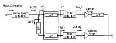
도 5는 본 발명의 제 3 실시 예에 따라 새로운 입력 정합 방법과 출력 정합 방법을 함께 적용한 도허티 전력 증폭 장치의 회로도로서, 도 2 및 도 4와 비교할 때에 동일한 구성요소에 대해서는 동일한 참조부호를 명기하였다.FIG. 5 is a circuit diagram of a Doherty power amplifying apparatus using a new input matching method and an output matching method according to a third embodiment of the present invention, and the same reference numerals are designated for the same components when compared to FIGS. 2 and 4. .
도 5를 참조하여 본 발명에 따른 입력 정합 방법과 출력 정합 방법이 함께 적용된 도허티 전력 증폭 장치의 구성을 살펴보면, 병렬로 연결한 캐리어 증폭기(110) 및 피킹 증폭기(115), 캐리어 증폭기(110)와 피킹 증폭기(115)의 입력단에 각각 연결된 복수의 입력 정합 회로(170, 175), 캐리어 증폭기(110)의 출력단에 연결되어 캐리어 증폭기(110)의 로드 라인 임피던스를 조절하는 임피던스 조절 회로(130), 임피던스 조절 회로(130)와 피킹 증폭기(115)의 후단에 연결된 출력 정합 회로(150), 입력 정합 회로(175)의 전단에 연결되어 입력 전력레벨이 높아질 때에 캐리어 증폭기(110) 쪽보다 피킹 증폭기(115)로 쪽으로 더 많은 전력을 공급하는 전력 분배 회로(145), 입력 정합 회로(170)의 전단에 연결되어 전체적인 지연을 맞 춰주는 제 2 지연 회로(140)를 포함한다. 이러한 본 발명의 제 3 실시 예는 제 1 실시 예의 출력 정합 부분과 제 2 실시 예의 입력 정합 부분을 함께 적용한 것이기에 그 설명이 생략된 부분은 제 1 실시 예와 제 2 실시 예에 대한 설명으로부터 쉽게 이해할 수 있다.Looking at the configuration of the Doherty power amplification device is a combination of the input matching method and the output matching method according to the present invention with reference to Figure 5, the
도허티 전력 증폭 장치에서 캐리어 증폭기가 Class AB의 바이어스가 걸리는 반면, 피킹 증폭기는 Class B 이하의 바이어스가 걸려있다. 이는 낮은 파워 영역에서의 캐리어 증폭기만 켬으로써 전력 증폭기 효율을 높이기 위한 이유이다. 하지만 이 같은 이유로 최대(Maximum) 파워 레벨에서 캐리어 증폭기와는 달리 피킹 증폭기는 최대 전류 레벨까지 도달하지 못하게 된다. 그 결과 전형적인 도허티 전력 증폭 장치는 최대 파워 레벨에서 캐리어 증폭기의 포화상태에 도달로 인해 전체 전력 증폭기가 포화상태로 도달하게 되는데, 그 상태에서 피킹 증폭기는 최대 파워를 내지 못하게 되어서 전체적으로 소자의 최대 파워를 다 내지 못하게 되는 셈이다. 그래서 본 발명에서는 이 문제점을 해결하기 위한 도허티 전력 증폭 장치의 새로운 전력 분배 방식을 제안한다. 도 4a는 본 발명에 의한 도허티 전력 증폭 장치의 전력 분배 그래프이다. 높은 이득과 효율 및 선형성 향상을 위해, 낮은 파워에서는 전체 전력 증폭기의 주 역할을 하는 캐리어 증폭기로의 전력 분배를 좀 더 가져가고, 높은 파워에서는 캐리어 증폭기, 피킹 증폭기 둘 다 똑 같은 전력을 내기 위해 상대적으로 늦게 켜진 피킹 증폭기 쪽으로 좀더 많은 전력을 공급하는 전력 분배 구성을 한다. 도 4b는 출력 전력 대비 효율 그래프를 Class AB와 비교해서 나타내었다. 도 4c는 높은 효율을 위해 새로운 전력 분배 방식을 구현한 도허티 전력 증폭 장치 의 입력 정합 회로의 개념을 설명한 구성도이다. 앞서 설명 한 듯이, 도허티 전력 증폭 장치의 입력 정합의 소형화 및 집적화를 위한 방법에 피킹 증폭기, 캐리어 증폭기 입력 단에 쿼터 웨이브 트랜스포머를 각각 추가된 모습을 보여준다. 결과적으로 피킹 증폭기의 입력 단에는 두 개의 λ/4 트랜스포머가 배치되므로 λ/2 트랜스포머의 역할을 수행한다. 즉, 도 1과 같이 피킹 증폭기의 입력 단에 하나의 쿼터 웨이브 트랜스포머가 배치된 종래 기술의 도허티 전력 증폭 장치에 본 발명에 의해 또 하나의 쿼터 웨이브 트랜스포머가 추가되는 것이다.In Doherty power amplifiers, the carrier amplifier is biased at Class AB, while the peaking amplifier is biased at less than Class B. This is the reason for increasing the power amplifier efficiency by turning on only the carrier amplifier in the low power region. For this reason, however, unlike the carrier amplifier at the maximum power level, the peaking amplifier does not reach the maximum current level. As a result, a typical Doherty power amplification device reaches the saturation of the carrier amplifier at its maximum power level, causing the entire power amplifier to reach saturation, where the peaking amplifier is unable to produce full power, thereby reducing the overall power of the device. You can't get it all. Therefore, the present invention proposes a new power distribution scheme of the Doherty power amplifier for solving this problem. 4A is a power distribution graph of the Doherty power amplification apparatus according to the present invention. For higher gain, efficiency and linearity improvement, lower power takes more power distribution to the carrier amplifier, which is the main power amplifier, while at higher power, both the carrier amplifier and the peaking amplifier provide the same power. A power distribution scheme is used to provide more power towards the later turned on peaking amplifier. 4b shows the output power vs. efficiency graph compared to Class AB. Figure 4c is a block diagram illustrating the concept of the input matching circuit of the Doherty power amplifier for implementing a new power distribution scheme for high efficiency. As described above, the method for miniaturizing and integrating the input matching of the Doherty power amplification device is shown with a quarter wave transformer added to the picking amplifier and the carrier amplifier input stage, respectively. As a result, two λ / 4 transformers are arranged at the input stage of the peaking amplifier, thus serving as a λ / 2 transformer. That is, according to the present invention, another quarter wave transformer is added to the conventional Doherty power amplification apparatus in which one quarter wave transformer is disposed at the input terminal of the peaking amplifier as shown in FIG. 1.
도허티 전력 증폭 장치에서 캐리어 증폭기의 입력 임피던스(Zin_c)는 입력 전력레벨에 따라 크게 변하지 않는다. 반면에, 피킹 증폭기의 입력 임피던스(Zin_p)는 입력 전력레벨이 높아질수록 자기(Self) 바이어스 효과로 인해 작아지는 현상을 보인다. 이는 피킹 증폭기의 경우에 Class C 바이어스로 걸려있어, 낮은 전력레벨에서는 꺼져 있다가 일정 전력레벨이상이 되면 켜지면서 전류레벨이 증가하면서 생기는 현상이다. 본 발명에 의한 도허티 입력 전력 분배는 이 현상에 착안을 하였다. 전형적인 도허티 전력 증폭 장치에서는 피킹 증폭기 입력단의 쿼터 웨이브 트랜스포머 때문에 전력레벨이 높아짐에 따라 전력 분배가 되는 위치에서의 피킹 증폭기의 입력 임피던스가 커지게 된다. 이 때문에 전력 레벨이 높아질수록 피킹 증폭기로의 입력 전력이 캐리어 증폭기보다 작아지게 된다. 이는 앞서 말한 이상적인 도허티 증폭기의 전력 분배와 반대이다. 따라서 피킹 증폭기 입력단에 쿼터 웨이브 트랜스포머를 하나 더 추가하여서 기존의 피킹 증폭기의 입력 임피던스의 모습을 정반대로 원하는 방향으로 바꾸어 놓았다. 캐리어 증폭기의 입력단에도 전체적인 지연을 맞춰주기 위해 쿼터 웨이브 트랜스포머를 하나 더 추가하였다.In the Doherty power amplification device, the input impedance Zin_c of the carrier amplifier does not vary greatly depending on the input power level. On the other hand, the input impedance Zin_p of the peaking amplifier decreases due to the self bias effect as the input power level increases. This is caused by a Class C bias in the case of the peaking amplifier, which is turned off at a low power level and then increases when the current level increases when the power amplifier is above a certain power level. The Doherty input power distribution according to the present invention focuses on this phenomenon. In a typical Doherty power amplification device, due to the quarter-wave transformer at the input stage of the peaking amplifier, the input impedance of the peaking amplifier at the power distribution position increases as the power level increases. For this reason, the higher the power level, the smaller the input power to the peaking amplifier than the carrier amplifier. This is the opposite of the ideal power distribution of the ideal Doherty amplifier. Therefore, by adding another quarter-wave transformer to the input of the peaking amplifier, the input impedance of the conventional peaking amplifier is reversed in the desired direction. An additional quarter-wave transformer has been added to the input of the carrier amplifier to match the overall delay.
도 5는 본 발명의 내용을 토대로, 5GHz WLAN 응용을 위해 제작된 완전 집적된 도허티 전력 증폭기의 MMIC 전체 칩 사진이다.5 is a MMIC full chip photograph of a fully integrated Doherty power amplifier fabricated for 5 GHz WLAN applications, based on the teachings of the present invention.
지금까지 본 발명의 일 실시 예에 국한하여 설명하였으나 본 발명의 기술이 당업자에 의하여 용이하게 변형 실시될 가능성이 자명하다. 이러한 변형된 실시 예들은 본 발명의 특허청구범위에 기재된 기술사상에 당연히 포함되는 것으로 해석되어야 할 것이다.It has been described so far limited to one embodiment of the present invention, it is obvious that the technology of the present invention can be easily modified by those skilled in the art. Such modified embodiments should be construed as naturally included in the technical spirit described in the claims of the present invention.
전술한 바와 같이 본 발명은 도허티 전력 증폭 장치의 새로운 출력 정합 방법과 입력 정합 방법을 제공함으로써, 효율과 선형성 측면에서 큰 장점을 가진 도허티 전력 증폭 장치를 소형화 및 집적화 할 수 있도록 하며, 새로운 입력 전력 분배 방법을 적용하여 좀더 이상적인 도허티 동작이 일어나게 하는 효과가 있다.As described above, the present invention provides a new output matching method and an input matching method of the Doherty power amplification device, thereby miniaturizing and integrating the Doherty power amplification device having great advantages in terms of efficiency and linearity, and new input power distribution. By applying the method, there is an effect that a more ideal Doherty operation occurs.
Claims (20)
Translated fromKoreanPriority Applications (5)
| Application Number | Priority Date | Filing Date | Title |
|---|---|---|---|
| KR1020060050788AKR100749870B1 (en) | 2006-06-07 | 2006-06-07 | Doherty power amplifier |
| US12/302,207US7973600B2 (en) | 2006-06-07 | 2007-05-18 | Doherty power amplifier |
| CN2007800211299ACN101467346B (en) | 2006-06-07 | 2007-05-18 | Doherty power amplifier |
| PCT/KR2007/002424WO2007142414A1 (en) | 2006-06-07 | 2007-05-18 | Doherty power amplifier |
| TW096120197ATWI462469B (en) | 2006-06-07 | 2007-06-05 | Doherty power amplifier |
Applications Claiming Priority (1)
| Application Number | Priority Date | Filing Date | Title |
|---|---|---|---|
| KR1020060050788AKR100749870B1 (en) | 2006-06-07 | 2006-06-07 | Doherty power amplifier |
Publications (1)
| Publication Number | Publication Date |
|---|---|
| KR100749870B1true KR100749870B1 (en) | 2007-08-17 |
Family
ID=38614681
Family Applications (1)
| Application Number | Title | Priority Date | Filing Date |
|---|---|---|---|
| KR1020060050788AActiveKR100749870B1 (en) | 2006-06-07 | 2006-06-07 | Doherty power amplifier |
Country Status (5)
| Country | Link |
|---|---|
| US (1) | US7973600B2 (en) |
| KR (1) | KR100749870B1 (en) |
| CN (1) | CN101467346B (en) |
| TW (1) | TWI462469B (en) |
| WO (1) | WO2007142414A1 (en) |
Cited By (6)
| Publication number | Priority date | Publication date | Assignee | Title |
|---|---|---|---|---|
| WO2009045686A3 (en)* | 2007-09-28 | 2010-07-22 | Motorola, Inc. | Inverted doherty amplifier with increased off-state impedence |
| US7936213B2 (en) | 2008-08-28 | 2011-05-03 | Xronet Corporation | Doherty amplifier and signal amplification system having the same, method for amplifying signal |
| KR101091969B1 (en)* | 2009-06-01 | 2011-12-09 | 포항공과대학교 산학협력단 | Power amplifier apparatus |
| EP2227860A4 (en)* | 2007-12-05 | 2012-02-15 | Ericsson Telefon Ab L M | Load modulation arrangement |
| KR20160066593A (en)* | 2014-12-02 | 2016-06-13 | 전자부품연구원 | Broadband Doherty Power Amplifier |
| KR20160141311A (en)* | 2015-05-29 | 2016-12-08 | 삼성전기주식회사 | Doherty Power Amplifier |
Families Citing this family (40)
| Publication number | Priority date | Publication date | Assignee | Title |
|---|---|---|---|---|
| EP2329592A1 (en)* | 2008-07-09 | 2011-06-08 | ST Wireless SA | Doherty amplifier with input network optimized for mmic |
| US7961048B2 (en)* | 2008-12-12 | 2011-06-14 | Samsung Electro-Mechanics Company | Integrated power amplifiers for use in wireless communication devices |
| CN101834572A (en)* | 2010-05-14 | 2010-09-15 | 北京瑞夫艾电子有限公司 | Broadband radio-frequency combining power amplifier |
| US9115363B2 (en)* | 2011-03-09 | 2015-08-25 | Ondek Pty Ltd | Gene expression and eradication system in Helicobacter pylori |
| US8339201B1 (en)* | 2011-06-17 | 2012-12-25 | Infineon Technologies Ag | Wideband doherty amplifier circuit having a constant impedance combiner |
| US8643433B2 (en)* | 2011-06-30 | 2014-02-04 | Broadcom Corporation | Bypass power amplifier for improving efficiency at low power |
| EP2820440B1 (en)* | 2012-03-02 | 2021-05-12 | Koninklijke Philips N.V. | Apparatus and method for amplifying a radio-frequency signal |
| JP5586653B2 (en)* | 2012-05-02 | 2014-09-10 | 株式会社東芝 | Doherty circuit |
| EP2698918A1 (en)* | 2012-08-14 | 2014-02-19 | Nxp B.V. | Amplifier circuit |
| CN103107778B (en)* | 2012-12-31 | 2016-03-02 | 东南大学 | A kind of Doherty power amplifier and adjustment method thereof reducing third order intermodulation |
| WO2014108716A1 (en)* | 2013-01-10 | 2014-07-17 | Freescale Semiconductor, Inc. | Doherty amplifier |
| CN103457540B (en)* | 2013-09-06 | 2016-03-16 | 西安空间无线电技术研究所 | A kind of microwave power amplifier of Doherty structure |
| WO2015100739A1 (en)* | 2014-01-06 | 2015-07-09 | 华为技术有限公司 | Doherty power amplifier, communication device and system |
| CN105024651B (en)* | 2014-04-29 | 2019-03-15 | 瑞昱半导体股份有限公司 | Radio frequency power amplifier and method for improving power added efficiency and linearity |
| EP2958232A1 (en)* | 2014-06-18 | 2015-12-23 | Nxp B.V. | Doherty amplifier |
| JP6316506B2 (en)* | 2015-06-15 | 2018-04-25 | 株式会社日立国際電気 | Power amplifier and wireless transmitter |
| CN108141179B (en)* | 2016-02-17 | 2021-10-15 | 株式会社村田制作所 | Power amplifier |
| TWI580176B (en)* | 2016-07-21 | 2017-04-21 | With automatic adjustment of the main and auxiliary amplifier power ratio than the Doher power amplifier | |
| US10211784B2 (en)* | 2016-11-03 | 2019-02-19 | Nxp Usa, Inc. | Amplifier architecture reconfiguration |
| US9966903B1 (en)* | 2016-12-30 | 2018-05-08 | Nxp Usa, Inc. | Doherty architecture for wideband power amplifier design |
| US11233483B2 (en)* | 2017-02-02 | 2022-01-25 | Macom Technology Solutions Holdings, Inc. | 90-degree lumped and distributed Doherty impedance inverter |
| US11050389B2 (en)* | 2017-04-24 | 2021-06-29 | Macom Technology Solutions Holdings, Inc. | Inverted Doherty power amplifier with large RF and instantaneous bandwidths |
| US11245363B2 (en) | 2017-04-24 | 2022-02-08 | Macom Technology Solutions Holdings, Inc. | Efficiency, symmetrical Doherty power amplifier |
| WO2018197917A1 (en) | 2017-04-24 | 2018-11-01 | Macom Technology Solutions Holdings, Inc. | Inverted doherty power amplifier with large rf fractional and instantaneous bandwiths |
| CN107332528A (en)* | 2017-08-11 | 2017-11-07 | 华中科技大学 | A kind of tunable multiple frequency section power amplifier |
| FR3070100A1 (en) | 2017-08-14 | 2019-02-15 | Macom Technology Solutions Holdings, Inc. | POWERFUL AMPLIFIER ARCHITECTURE WITHOUT MODULATION, BROADBAND AND HIGH EFFICIENCY |
| EP3692631A1 (en) | 2017-10-02 | 2020-08-12 | MACOM Technology Solutions Holdings, Inc. | No-load-modulation, high-efficiency power amplifier |
| CN107733372A (en)* | 2017-11-07 | 2018-02-23 | 南京国博电子有限公司 | A kind of broadband Doherty power amplifier |
| CN110380691B (en)* | 2018-04-12 | 2024-11-05 | 南京中兴新软件有限责任公司 | A power amplifier circuit and device based on Doherty power amplifier |
| CN110417355B (en)* | 2018-04-26 | 2023-11-07 | 苏州远创达科技有限公司 | Integrated high-resistance wire doherty amplifier |
| CN108599727B (en)* | 2018-05-09 | 2020-11-06 | 上海大学 | High-efficiency broadband Doherty power amplifier |
| CN112640298A (en) | 2018-10-05 | 2021-04-09 | 镁可微波技术有限公司 | Low load modulation power amplifier |
| JP2021061577A (en)* | 2019-10-09 | 2021-04-15 | 株式会社村田製作所 | High frequency module and communication device |
| US11888448B2 (en) | 2019-12-30 | 2024-01-30 | Macom Technology Solutions Holdings, Inc. | Low-load-modulation broadband amplifier |
| US12028022B2 (en) | 2020-12-10 | 2024-07-02 | Macom Technology Solutions Holdings, Inc. | Hybrid power amplifier with GaN-on-Si and GaN-on-SiC circuits |
| CN112564648A (en)* | 2021-02-09 | 2021-03-26 | 广州慧智微电子有限公司 | Power amplifier, chip and equipment |
| CN216390920U (en)* | 2021-11-05 | 2022-04-26 | 深圳飞骧科技股份有限公司 | Doherty radio frequency power amplifier |
| CN115882791B (en)* | 2022-12-12 | 2025-08-01 | 深圳飞骧科技股份有限公司 | Voltage synthesis type Doherty power amplifier |
| CN115913128B (en)* | 2022-12-31 | 2024-04-23 | 尚睿微电子(上海)有限公司 | Doherty power amplifier, radio frequency chip and electronic equipment |
| CN118157594A (en)* | 2024-02-08 | 2024-06-07 | 北京昂瑞微电子技术股份有限公司 | Broadband Doherty Power Amplifier |
Citations (6)
| Publication number | Priority date | Publication date | Assignee | Title |
|---|---|---|---|---|
| US6356149B1 (en)* | 2000-04-10 | 2002-03-12 | Motorola, Inc. | Tunable inductor circuit, phase tuning circuit and applications thereof |
| KR20020074630A (en)* | 2001-03-21 | 2002-10-04 | 학교법인 포항공과대학교 | Full output matching apparatus of the microwave doherty amplifier |
| KR20030065873A (en)* | 2002-02-01 | 2003-08-09 | 주식회사 웨이브아이씨스 | Power Amplification Apparatus of Portable Terminal |
| JP2004120086A (en)* | 2002-09-24 | 2004-04-15 | Mitsubishi Electric Corp | High frequency power amplifier |
| KR20050093821A (en)* | 2003-01-09 | 2005-09-23 | 닛본 덴끼 가부시끼가이샤 | Doherty amplifier |
| US20060097783A1 (en)* | 2004-11-05 | 2006-05-11 | Hitachi Kokusai Electric Inc. | Amplifier |
Family Cites Families (15)
| Publication number | Priority date | Publication date | Assignee | Title |
|---|---|---|---|---|
| US6262629B1 (en)* | 1999-07-06 | 2001-07-17 | Motorola, Inc. | High efficiency power amplifier having reduced output matching networks for use in portable devices |
| US6320462B1 (en)* | 2000-04-12 | 2001-11-20 | Raytheon Company | Amplifier circuit |
| US6731172B2 (en)* | 2001-01-16 | 2004-05-04 | Skyworks Solutions, Inc. | Doherty power amplifier with integrated quarter wave transformer/combiner circuit |
| US6424223B1 (en)* | 2001-01-19 | 2002-07-23 | Eic Corporation | MMIC power amplifier with wirebond output matching circuit |
| US6864742B2 (en)* | 2001-06-08 | 2005-03-08 | Northrop Grumman Corporation | Application of the doherty amplifier as a predistortion circuit for linearizing microwave amplifiers |
| US6737922B2 (en)* | 2002-01-28 | 2004-05-18 | Cree Microwave, Inc. | N-way RF power amplifier circuit with increased back-off capability and power added efficiency using unequal input power division |
| CN100477494C (en)* | 2002-08-19 | 2009-04-08 | Nxp股份有限公司 | High Power Doherty Amplifier |
| KR100450744B1 (en)* | 2002-08-29 | 2004-10-01 | 학교법인 포항공과대학교 | Doherty amplifier |
| KR20050031663A (en)* | 2003-09-30 | 2005-04-06 | 광운대학교 산학협력단 | Doherty power amplifying apparatus |
| JP4520204B2 (en)* | 2004-04-14 | 2010-08-04 | 三菱電機株式会社 | High frequency power amplifier |
| JP4715994B2 (en)* | 2004-08-26 | 2011-07-06 | 日本電気株式会社 | Doherty amplifier parallel operation circuit |
| CN101494439B (en)* | 2004-11-05 | 2012-03-28 | 株式会社日立国际电气 | amplifier |
| KR20060077818A (en)* | 2004-12-31 | 2006-07-05 | 학교법인 포항공과대학교 | Power amplification device using asymmetric power drive |
| US7295074B2 (en)* | 2005-03-31 | 2007-11-13 | Beceem Communications Inc. | Doherty power amplifier with phase compensation |
| US7336127B2 (en)* | 2005-06-10 | 2008-02-26 | Rf Micro Devices, Inc. | Doherty amplifier configuration for a collector controlled power amplifier |
- 2006
- 2006-06-07KRKR1020060050788Apatent/KR100749870B1/enactiveActive
- 2007
- 2007-05-18WOPCT/KR2007/002424patent/WO2007142414A1/enactiveApplication Filing
- 2007-05-18CNCN2007800211299Apatent/CN101467346B/enactiveActive
- 2007-05-18USUS12/302,207patent/US7973600B2/enactiveActive
- 2007-06-05TWTW096120197Apatent/TWI462469B/enactive
Patent Citations (6)
| Publication number | Priority date | Publication date | Assignee | Title |
|---|---|---|---|---|
| US6356149B1 (en)* | 2000-04-10 | 2002-03-12 | Motorola, Inc. | Tunable inductor circuit, phase tuning circuit and applications thereof |
| KR20020074630A (en)* | 2001-03-21 | 2002-10-04 | 학교법인 포항공과대학교 | Full output matching apparatus of the microwave doherty amplifier |
| KR20030065873A (en)* | 2002-02-01 | 2003-08-09 | 주식회사 웨이브아이씨스 | Power Amplification Apparatus of Portable Terminal |
| JP2004120086A (en)* | 2002-09-24 | 2004-04-15 | Mitsubishi Electric Corp | High frequency power amplifier |
| KR20050093821A (en)* | 2003-01-09 | 2005-09-23 | 닛본 덴끼 가부시끼가이샤 | Doherty amplifier |
| US20060097783A1 (en)* | 2004-11-05 | 2006-05-11 | Hitachi Kokusai Electric Inc. | Amplifier |
Cited By (8)
| Publication number | Priority date | Publication date | Assignee | Title |
|---|---|---|---|---|
| WO2009045686A3 (en)* | 2007-09-28 | 2010-07-22 | Motorola, Inc. | Inverted doherty amplifier with increased off-state impedence |
| EP2227860A4 (en)* | 2007-12-05 | 2012-02-15 | Ericsson Telefon Ab L M | Load modulation arrangement |
| US7936213B2 (en) | 2008-08-28 | 2011-05-03 | Xronet Corporation | Doherty amplifier and signal amplification system having the same, method for amplifying signal |
| KR101091969B1 (en)* | 2009-06-01 | 2011-12-09 | 포항공과대학교 산학협력단 | Power amplifier apparatus |
| KR20160066593A (en)* | 2014-12-02 | 2016-06-13 | 전자부품연구원 | Broadband Doherty Power Amplifier |
| KR101654927B1 (en)* | 2014-12-02 | 2016-09-08 | 전자부품연구원 | Broadband Doherty power amplifier |
| KR20160141311A (en)* | 2015-05-29 | 2016-12-08 | 삼성전기주식회사 | Doherty Power Amplifier |
| KR102140192B1 (en) | 2015-05-29 | 2020-08-03 | 삼성전기주식회사 | Doherty power amplifier |
Also Published As
| Publication number | Publication date |
|---|---|
| CN101467346B (en) | 2012-12-05 |
| US20090273398A1 (en) | 2009-11-05 |
| TW200828784A (en) | 2008-07-01 |
| TWI462469B (en) | 2014-11-21 |
| WO2007142414A1 (en) | 2007-12-13 |
| US7973600B2 (en) | 2011-07-05 |
| CN101467346A (en) | 2009-06-24 |
| WO2007142414A8 (en) | 2008-06-05 |
Similar Documents
| Publication | Publication Date | Title |
|---|---|---|
| KR100749870B1 (en) | Doherty power amplifier | |
| Cao et al. | Continuous-mode hybrid asymmetrical load-modulated balanced amplifier with three-way modulation and multi-band reconfigurability | |
| US9917551B2 (en) | Doherty amplifiers with minimum phase output networks | |
| US10211785B2 (en) | Doherty amplifiers with passive phase compensation circuits | |
| CN101388648B (en) | Multi-frequency multi-mode power amplifier circuit and its operation method | |
| KR100862056B1 (en) | Broadband power amplifier | |
| US7358806B2 (en) | Method and apparatus for an improved power amplifier | |
| US8581665B2 (en) | Doherty amplifier | |
| US7242245B2 (en) | Method and apparatus for an improved power amplifier | |
| CN100542011C (en) | Integrated Doherty-type amplifier device with high power efficiency | |
| CN103312272B (en) | Multi-mode doherty power amplifier | |
| CN106664062B (en) | Integrated 3-way Doherty amplifier | |
| US10742173B2 (en) | Systems and methods for fast switching time division duplex operation of power amplifiers | |
| JP5313970B2 (en) | High frequency power amplifier | |
| US7501897B2 (en) | High-power amplifier | |
| KR20060058423A (en) | Doherty amplifier in series without hybrid coupler | |
| Chen et al. | Fully-integrated broadband GaAs MMIC load modulated balanced amplifier for sub-6 GHz applications | |
| US10630242B2 (en) | Doherty amplifiers with passive phase compensation circuits | |
| US7248109B2 (en) | Method and apparatus for an improved power amplifier | |
| CN100533952C (en) | High Frequency Power Amplifier Components | |
| CN223348637U (en) | Radio frequency power amplifying circuit based on balanced power amplifying structure | |
| US20060006934A1 (en) | Method and apparatus for an improved power amplifier | |
| US20240364271A1 (en) | Inverted doherty-type amplifier device | |
| US20250132732A1 (en) | Amplifier device having a tunable element and method therefor | |
| EP1854208A2 (en) | Method and apparatus for an improved power amplifier |
Legal Events
| Date | Code | Title | Description |
|---|---|---|---|
| A201 | Request for examination | ||
| PA0109 | Patent application | Patent event code:PA01091R01D Comment text:Patent Application Patent event date:20060607 | |
| PA0201 | Request for examination | ||
| N231 | Notification of change of applicant | ||
| PN2301 | Change of applicant | Patent event date:20070518 Comment text:Notification of Change of Applicant Patent event code:PN23011R01D | |
| E701 | Decision to grant or registration of patent right | ||
| PE0701 | Decision of registration | Patent event code:PE07011S01D Comment text:Decision to Grant Registration Patent event date:20070727 | |
| GRNT | Written decision to grant | ||
| PR0701 | Registration of establishment | Comment text:Registration of Establishment Patent event date:20070809 Patent event code:PR07011E01D | |
| PR1002 | Payment of registration fee | Payment date:20070810 End annual number:3 Start annual number:1 | |
| PG1601 | Publication of registration | ||
| PR1001 | Payment of annual fee | Payment date:20100731 Start annual number:4 End annual number:4 | |
| PR1001 | Payment of annual fee | Payment date:20110801 Start annual number:5 End annual number:5 | |
| PR1001 | Payment of annual fee | Payment date:20120531 Start annual number:6 End annual number:6 | |
| FPAY | Annual fee payment | Payment date:20130531 Year of fee payment:7 | |
| PR1001 | Payment of annual fee | Payment date:20130531 Start annual number:7 End annual number:7 | |
| FPAY | Annual fee payment | Payment date:20140530 Year of fee payment:8 | |
| PR1001 | Payment of annual fee | Payment date:20140530 Start annual number:8 End annual number:8 | |
| FPAY | Annual fee payment | Payment date:20150529 Year of fee payment:9 | |
| PR1001 | Payment of annual fee | Payment date:20150529 Start annual number:9 End annual number:9 | |
| FPAY | Annual fee payment | Payment date:20160630 Year of fee payment:10 | |
| PR1001 | Payment of annual fee | Payment date:20160630 Start annual number:10 End annual number:10 | |
| PR1001 | Payment of annual fee | Payment date:20200615 Start annual number:14 End annual number:14 | |
| PR1001 | Payment of annual fee | Payment date:20210615 Start annual number:15 End annual number:15 | |
| PR1001 | Payment of annual fee | Payment date:20230614 Start annual number:17 End annual number:17 |