KR100748261B1 - FINE field effect transistor with low leakage current and its manufacturing method - Google Patents
FINE field effect transistor with low leakage current and its manufacturing methodDownload PDFInfo
- Publication number
- KR100748261B1 KR100748261B1KR1020060084370AKR20060084370AKR100748261B1KR 100748261 B1KR100748261 B1KR 100748261B1KR 1020060084370 AKR1020060084370 AKR 1020060084370AKR 20060084370 AKR20060084370 AKR 20060084370AKR 100748261 B1KR100748261 B1KR 100748261B1
- Authority
- KR
- South Korea
- Prior art keywords
- gate electrode
- insulating film
- gate
- fence
- forming
- Prior art date
- Legal status (The legal status is an assumption and is not a legal conclusion. Google has not performed a legal analysis and makes no representation as to the accuracy of the status listed.)
- Active
Links
- 230000005669field effectEffects0.000titleclaimsabstractdescription48
- 238000004519manufacturing processMethods0.000titleclaimsabstractdescription37
- 239000000758substrateSubstances0.000claimsabstractdescription104
- 230000006870functionEffects0.000claimsabstractdescription66
- XUIMIQQOPSSXEZ-UHFFFAOYSA-NSiliconChemical compound[Si]XUIMIQQOPSSXEZ-UHFFFAOYSA-N0.000claimsabstractdescription57
- 229910052710siliconInorganic materials0.000claimsabstractdescription57
- 239000010703siliconSubstances0.000claimsabstractdescription57
- 239000000463materialSubstances0.000claimsabstractdescription29
- 238000000059patterningMethods0.000claimsabstractdescription17
- 239000010408filmSubstances0.000claimsdescription403
- 229910021420polycrystalline siliconInorganic materials0.000claimsdescription64
- 150000004767nitridesChemical class0.000claimsdescription48
- 238000005530etchingMethods0.000claimsdescription42
- 238000000034methodMethods0.000claimsdescription35
- 238000002955isolationMethods0.000claimsdescription24
- 238000005468ion implantationMethods0.000claimsdescription19
- 229920005591polysiliconPolymers0.000claimsdescription19
- 239000002184metalSubstances0.000claimsdescription18
- 229910052751metalInorganic materials0.000claimsdescription18
- 229920002120photoresistant polymerPolymers0.000claimsdescription16
- 238000000137annealingMethods0.000claimsdescription15
- 239000004065semiconductorSubstances0.000claimsdescription15
- 230000000694effectsEffects0.000claimsdescription14
- 230000008569processEffects0.000claimsdescription14
- 125000006850spacer groupChemical group0.000claimsdescription14
- 238000000151depositionMethods0.000claimsdescription8
- 239000012777electrically insulating materialSubstances0.000claimsdescription8
- 239000012535impuritySubstances0.000claimsdescription7
- 229910021421monocrystalline siliconInorganic materials0.000claimsdescription7
- 229910000577Silicon-germaniumInorganic materials0.000claimsdescription6
- 230000001590oxidative effectEffects0.000claimsdescription6
- -1polycrystalline GeInorganic materials0.000claimsdescription6
- 238000000206photolithographyMethods0.000claimsdescription4
- ATJFFYVFTNAWJD-UHFFFAOYSA-NTinChemical compound[Sn]ATJFFYVFTNAWJD-UHFFFAOYSA-N0.000claimsdescription3
- 229910021417amorphous siliconInorganic materials0.000claimsdescription3
- 239000012212insulatorSubstances0.000claimsdescription3
- 229910044991metal oxideInorganic materials0.000claimsdescription3
- 150000004706metal oxidesChemical class0.000claimsdescription3
- 229910021332silicideInorganic materials0.000claimsdescription3
- 239000013078crystalSubstances0.000claimsdescription2
- 230000003071parasitic effectEffects0.000claimsdescription2
- 239000010409thin filmSubstances0.000claimsdescription2
- 208000031872Body RemainsDiseases0.000claims1
- 229910002056binary alloyInorganic materials0.000claims1
- FVBUAEGBCNSCDD-UHFFFAOYSA-Nsilicide(4-)Chemical compound[Si-4]FVBUAEGBCNSCDD-UHFFFAOYSA-N0.000claims1
- 230000008719thickeningEffects0.000claims1
- 230000005684electric fieldEffects0.000description6
- 150000002739metalsChemical class0.000description6
- 230000008859changeEffects0.000description4
- 230000010354integrationEffects0.000description3
- 230000004888barrier functionEffects0.000description2
- 230000015572biosynthetic processEffects0.000description2
- 210000000746body regionAnatomy0.000description2
- 230000007423decreaseEffects0.000description2
- 230000003247decreasing effectEffects0.000description2
- 238000005516engineering processMethods0.000description2
- 238000012986modificationMethods0.000description2
- 230000004048modificationEffects0.000description2
- 230000005641tunnelingEffects0.000description2
- UFHFLCQGNIYNRP-UHFFFAOYSA-NHydrogenChemical compound[H][H]UFHFLCQGNIYNRP-UHFFFAOYSA-N0.000description1
- 230000001154acute effectEffects0.000description1
- 230000007547defectEffects0.000description1
- 238000010292electrical insulationMethods0.000description1
- 239000007789gasSubstances0.000description1
- 239000001257hydrogenSubstances0.000description1
- 229910052739hydrogenInorganic materials0.000description1
- 230000014759maintenance of locationEffects0.000description1
- 238000013507mappingMethods0.000description1
- 239000002105nanoparticleSubstances0.000description1
- 230000003647oxidationEffects0.000description1
- 238000007254oxidation reactionMethods0.000description1
- 230000002093peripheral effectEffects0.000description1
- 230000009467reductionEffects0.000description1
- 238000011160researchMethods0.000description1
- 238000012552reviewMethods0.000description1
- 230000035945sensitivityEffects0.000description1
- 238000005549size reductionMethods0.000description1
- 239000000779smokeSubstances0.000description1
Images


Classifications
- H—ELECTRICITY
- H10—SEMICONDUCTOR DEVICES; ELECTRIC SOLID-STATE DEVICES NOT OTHERWISE PROVIDED FOR
- H10D—INORGANIC ELECTRIC SEMICONDUCTOR DEVICES
- H10D30/00—Field-effect transistors [FET]
- H10D30/60—Insulated-gate field-effect transistors [IGFET]
- H10D30/62—Fin field-effect transistors [FinFET]
- H10D30/6211—Fin field-effect transistors [FinFET] having fin-shaped semiconductor bodies integral with the bulk semiconductor substrates
- H—ELECTRICITY
- H10—SEMICONDUCTOR DEVICES; ELECTRIC SOLID-STATE DEVICES NOT OTHERWISE PROVIDED FOR
- H10D—INORGANIC ELECTRIC SEMICONDUCTOR DEVICES
- H10D30/00—Field-effect transistors [FET]
- H10D30/01—Manufacture or treatment
- H10D30/021—Manufacture or treatment of FETs having insulated gates [IGFET]
- H10D30/024—Manufacture or treatment of FETs having insulated gates [IGFET] of fin field-effect transistors [FinFET]
- H—ELECTRICITY
- H10—SEMICONDUCTOR DEVICES; ELECTRIC SOLID-STATE DEVICES NOT OTHERWISE PROVIDED FOR
- H10D—INORGANIC ELECTRIC SEMICONDUCTOR DEVICES
- H10D30/00—Field-effect transistors [FET]
- H10D30/60—Insulated-gate field-effect transistors [IGFET]
- H10D30/611—Insulated-gate field-effect transistors [IGFET] having multiple independently-addressable gate electrodes influencing the same channel
- H—ELECTRICITY
- H10—SEMICONDUCTOR DEVICES; ELECTRIC SOLID-STATE DEVICES NOT OTHERWISE PROVIDED FOR
- H10D—INORGANIC ELECTRIC SEMICONDUCTOR DEVICES
- H10D30/00—Field-effect transistors [FET]
- H10D30/60—Insulated-gate field-effect transistors [IGFET]
- H10D30/67—Thin-film transistors [TFT]
- H10D30/6729—Thin-film transistors [TFT] characterised by the electrodes
- H10D30/6737—Thin-film transistors [TFT] characterised by the electrodes characterised by the electrode materials
- H10D30/6739—Conductor-insulator-semiconductor electrodes
- H—ELECTRICITY
- H10—SEMICONDUCTOR DEVICES; ELECTRIC SOLID-STATE DEVICES NOT OTHERWISE PROVIDED FOR
- H10D—INORGANIC ELECTRIC SEMICONDUCTOR DEVICES
- H10D64/00—Electrodes of devices having potential barriers
- H10D64/60—Electrodes characterised by their materials
- H10D64/66—Electrodes having a conductor capacitively coupled to a semiconductor by an insulator, e.g. MIS electrodes
- H10D64/671—Electrodes having a conductor capacitively coupled to a semiconductor by an insulator, e.g. MIS electrodes the conductor having lateral variation in doping or structure
- H—ELECTRICITY
- H10—SEMICONDUCTOR DEVICES; ELECTRIC SOLID-STATE DEVICES NOT OTHERWISE PROVIDED FOR
- H10D—INORGANIC ELECTRIC SEMICONDUCTOR DEVICES
- H10D30/00—Field-effect transistors [FET]
- H10D30/60—Insulated-gate field-effect transistors [IGFET]
- H10D30/62—Fin field-effect transistors [FinFET]
- H10D30/6212—Fin field-effect transistors [FinFET] having fin-shaped semiconductor bodies having non-rectangular cross-sections
- H10D30/6213—Fin field-effect transistors [FinFET] having fin-shaped semiconductor bodies having non-rectangular cross-sections having rounded corners
Landscapes
- Thin Film Transistor (AREA)
- Insulated Gate Type Field-Effect Transistor (AREA)
- Semiconductor Memories (AREA)
Abstract
Translated fromKoreanDescription
Translated fromKorean도 1은 종래의 기술에 따른 SOI 이중-게이트 소자의 일 실시형태를 도시한 단면도이다.1 is a cross-sectional view showing one embodiment of a SOI double-gate device according to the prior art.
도 2는 종래의 기술에 따른 SOI 이중-게이트 소자의 다른 실시형태를 도시한 단면도이다.2 is a cross-sectional view showing another embodiment of a SOI double-gate device according to the prior art.
도 3의 (a)는 종래의 기술에 따라 벌크(bulk) 기판에 구현된 측면 게이트를 가진 소자를 도시한 단면도이며, 도 3의 (b) 종래의 기술에 따른 SOI 이중-게이트 소자의 또 다른 실시형태를 도시한 단면도이다.Figure 3 (a) is a cross-sectional view showing a device having a side gate implemented on a bulk substrate in accordance with the prior art, Figure 3 (b) another of the SOI double-gate device according to the prior art It is sectional drawing which shows embodiment.
도 4는 본 발명의 바람직한 제1 실시예에 따른 FinFET을 도시한 것으로서, (a)는 사시도이며, (b)는 평면도이며, (c)는 A-A' 방향을 따라 절개하여 도시한 단면도이다.4 illustrates a FinFET according to a first preferred embodiment of the present invention, where (a) is a perspective view, (b) is a plan view, and (c) is a cross-sectional view taken along the A-A 'direction.
도 5는 본 발명의 바람직한 제1 실시예에 따른 FinFET의 제조 공정을 순차적으로 도시한 흐름도이다.5 is a flowchart sequentially illustrating a manufacturing process of the FinFET according to the first embodiment of the present invention.
도 6은 본 발명의 바람직한 제1 실시예에 따른 FinFET을 제조하는 과정을 순차적으로 도시한 단면도들이다.6 is a cross-sectional view sequentially illustrating a process of manufacturing a FinFET according to a first embodiment of the present invention.
도 7은 본 발명의 바람직한 제1 실시예의 일례에 따른 FinFET의 게이트 전극 형성 과정을 순차적으로 도시한 단면도들이다.7 is a cross-sectional view sequentially illustrating a process of forming a gate electrode of a FinFET according to an example of the first exemplary embodiment of the present invention.
도 8은 본 발명의 제2 실시예에 따른 FinFET을 도시한 것으로서, (a)는 사시도이며, (b)는 B-B' 방향을 따라 절개하여 도시한 단면도이다.FIG. 8 illustrates a FinFET according to a second embodiment of the present invention, where (a) is a perspective view and (b) is a cross-sectional view taken along the B-B 'direction.
도 9는 본 발명의 제2 실시예에 따른 FinFET을 제조하는 과정을 순차적으로 도시한 단면도들이다.9 is a cross-sectional view sequentially illustrating a process of manufacturing a FinFET according to a second embodiment of the present invention.
도 10은 본 발명의 제3 실시예에 따른 FinFET을 도시한 것으로서, (a)는 사시도이며, (b)는 평면도이다.10 illustrates a FinFET according to a third embodiment of the present invention, where (a) is a perspective view and (b) is a plan view.
도 11은 본 발명의 제4 실시예에 따른 FinFET을 도시한 것으로서, (a)는 사시도이며, (b)는 평면도이다.11 shows a FinFET according to a fourth embodiment of the present invention, where (a) is a perspective view and (b) is a plan view.
도 12는 본 발명의 제5 실시예에 따른 FinFET을 도시한 것으로서, (a)는 사시도이며, (b)는 평면도이다.12 shows a FinFET according to a fifth embodiment of the present invention, where (a) is a perspective view and (b) is a plan view.
도 13은 본 발명에 따른 FinFET의 담장형 바디의 상부 영역에 대한 실시 형태들을 예시적으로 도시한 것으로서, (a)는 담장형 바디의 상부면이 모서리가 진 형태를 도시한 단면도이며, (b)는 담장형 바디의 상부면이 둥글게 된 형태를 도시한 단면도이다.FIG. 13 exemplarily illustrates embodiments of an upper region of a fenced body of a FinFET according to the present invention, (a) is a cross-sectional view showing a cornered shape of an upper surface of the fenced body, and (b) ) Is a cross-sectional view showing the rounded shape of the upper surface of the fence body.
도 14는 본 발명에 따른 FinFET의 담장면 바디의 하부 영역에 대한 실시 형태들을 예시적으로 도시한 단면도로서, (a)는 담장형 바디의 폭이 기판으로 가면서 점차 넓어지는 구조를 도시한 단면도이며, (b)는 담장형 바디의 폭이 위쪽에서는 거의 일정하다가 어느 정도 아래에서 기판으로 가면서 점차 넓어지는 구조를 도시 한 단면도이다.14 is a cross-sectional view showing exemplary embodiments of the lower region of the fence body of the FinFET according to the present invention, (a) is a cross-sectional view showing a structure in which the width of the fence body gradually widens to the substrate. , (b) is a cross-sectional view showing a structure in which the width of the fence body is substantially constant at the top, but gradually widens to the substrate from below.
도 15는 본 발명에 따른 FinFET에 있어서, 길이가 50 nm로 고정된 n+/p+ 다결정실리콘 게이트인 경우, n+ 다결정실리콘의 길이 변화에 따른 ID-VGS 특성을 도시한 그래프이다.FIG. 15 is a graph illustrating ID -VGS characteristics according to a change in length of n+ polysilicon in the case of a n+ / p+ polysilicon gate fixed to 50 nm in length in the FinFET according to the present invention.
도 16은 본 발명에 따른 FinFET에 있어서, 길이가 50 nm로 고정된 n+/p+ 다결정실리콘 게이트인 경우, n+ 다결정실리콘의 길이 변화에 따른 GIDL (Gate Induced Drain Leakage) 특성을 도시한 그래프이다.FIG. 16 is a graph illustrating GIDL (Gate Induced Drain Leakage) characteristics according to the change in length of n+ polysilicon in the case of n+ / p+ polysilicon gate having a fixed length of 50 nm in the FinFET according to the present invention. to be.
<도면의 주요 부분에 대한 부호의 설명><Explanation of symbols for main parts of the drawings>
40 : FinFET40: FinFET
410 : 담장형 기판410: fence type substrate
420 : 담장형 바디420: fence body
450 : 소자 격리막450: device isolation film
460 : 게이트 절연막460: gate insulating film
470 : 제1 게이트 전극470: first gate electrode
480 : 제2 게이트 전극480: second gate electrode
490, 492 : 소오스/드레인 영역490, 492 source / drain regions
본 발명은 낮은 누설 전류를 갖는 핀(Fin) 전계 효과 트랜지스터에 관한 것으로서, 더욱 구체적으로는 고집적 DRAM 셀 소자 중 벌크 실리콘 기판위에 형성된 핀 전계효과 트랜지스터에 있어서, 일함수가 다른 두 물질을 이용한 게이트 전극을 형성하되 드레인 영역과 겹치는 게이트 전극의 영역의 일함수를 낮춤으로써 GIDL(Gate Induced Drain Leakage)를 감소시킬 수 있도록 하는 핀 전계효과 트랜지스터 및 그 제조 방법에 관한 것이다.The present invention relates to a fin field effect transistor having a low leakage current. More specifically, in a fin field effect transistor formed on a bulk silicon substrate among high density DRAM cell devices, a gate electrode using two materials having different work functions is provided. The present invention relates to a fin field effect transistor and a method of manufacturing the same, which reduce the work induced drain leakage (GIDL) by lowering the work function of the region of the gate electrode overlapping the drain region.
DRAM 기술은 계속 실리콘 반도체 시장에서 큰 비중을 차지하고 있는 핵심기술로서, 세계적으로 차세대 DRAM을 개발하기 위한 연구를 매우 활발하게 진행되고 있으며, 점차 더 고집적화 되어지고 있다. 특히, DRAM 셀 소자의 게이트 길이는 셀의 축소화 및 집적도의 증가를 위해 계속 줄어들고 있다. 셀 소자 축소화에 있어 가장 큰 문제는 소위 짧은 채널 효과(Short Channel Effect)이다. 짧은 채널 효과에 의해 off 상태에서의 드레인 전류가 증가하는 문제가 있다.DRAM technology continues to be a major player in the silicon semiconductor market, and is actively researching and developing next-generation DRAMs around the world. In particular, the gate length of DRAM cell devices continues to shrink to reduce cell size and increase integration. The biggest problem in cell device miniaturization is the so-called short channel effect. There is a problem that the drain current in the off state increases due to the short channel effect.
종래의 기술에 따른 MOSFET(Metal-Oxide-Semiconductor Field Effect Transistor)는 평탄한 표면에 형성된 채널 구조를 갖고 있으며, 채널의 양쪽에 소스/드레인 영역이 형성되어 있다. 이러한 기존의 평탄 채널을 갖는 MOSFET은 100 nm 이하의 DRAM 기술에 적용되면서 상기 언급한 짧은 채널 효과를 겪고 있다. 통상 MOS 전계효과트랜지스터가 축소화되면서 같이 변화되어야 하는 것은 게이트 절연막의 두께 감소, 소스/드레인 접합의 깊이 감소, 채널 도우핑 농도의 증가 등이다. DRAM 셀 소자는 특성상 게이트 길이 감소에 따라 기존의 로직용 MOSFET에 비해 게 이트 절연막의 두께를 줄일 수 없고 또한 상대적으로 소스/드레인의 깊이를 얕게 할 수 없기 때문에 셀 소자 축소화에 있어 큰 문제를 갖고 있다. 또한 소자 축소화에 따라 소위 DIBL (Drain Induced Barrier Lowering)을 막기 위해서는 채널의 도우핑을 증가시켜야 하는데, 이 경우 채널과 드레인 사이의 전계가 증가하고 band-to-band 터널링에 의해 누설전류가 증가하게 된다. DRAM 셀 소자에서 드레인 전류의 off 상태 누설전류는 대략 1 fA 수준 또는 그 이하가 되어야 한다. 따라서 기존의 평탄채널을 가진 MOSFET으로서는 대략 70 nm 이하로 셀 소자의 게이트 길이를 줄이는 것도 매우 어려울 것으로 예상된다.The MOSFET (Metal-Oxide-Semiconductor Field Effect Transistor) according to the related art has a channel structure formed on a flat surface, and source / drain regions are formed on both sides of the channel. These conventional flat channel MOSFETs suffer from the short channel effects mentioned above as they are applied to DRAM technology of 100 nm or less. In general, MOS field effect transistors have to be reduced as they shrink, such as decreasing the thickness of the gate insulating layer, decreasing the depth of the source / drain junction, and increasing the channel doping concentration. DRAM cell devices have a big problem in downsizing cell devices because the gate gate thickness can not be reduced and the source / drain depth can not be made shallower than the conventional logic MOSFET due to the reduced gate length. . In addition, in order to prevent so-called drain induced barrier lowering (DIBL) as the device shrinks, the doping of the channel must be increased. In this case, the electric field between the channel and the drain increases and the leakage current increases due to band-to-band tunneling. . In the DRAM cell device, the off-state leakage current of the drain current should be approximately 1 fA or less. Therefore, it is expected to reduce the gate length of a cell device to about 70 nm or less with a conventional flat channel MOSFET.
기존의 평탄채널 구조를 갖는 소자가 DRAM 셀 소자로 사용될 때의 문제점 때문에 이를 극복하기 위한 연구가 많이 진행되고 있다. 연구의 방향은 3 차원 소자 구조 또는 채널이 더 이상 평탄하지 않는 소자 구조를 셀 소자로 연구하는 것이다. DRAM 셀 소자로 고려되고 있는 대표적인 소자는 함몰 채널 구조를 갖는 소자와 벌크 FinFET이며, 이들 각각의 특징을 아래에서 설명한다.Due to a problem when a device having a conventional flat channel structure is used as a DRAM cell device, a lot of researches are being conducted to overcome this problem. The direction of the study is to study cell structures with device structures in which three-dimensional device structures or channels are no longer flat. Representative devices considered as DRAM cell devices are devices having a recessed channel structure and a bulk FinFET, each of which is described below.
메모리 셀 소자에서 중요한 것은 2 차원 상의 표면에서 셀 면적을 줄이면서 on 전류는 크게 하고 off 전류를 줄이는 것이다. 전술한 함몰 채널 구조는 2 차원 상의 표면 면적은 늘어나지 않게 하면서 유효채널의 길이를 길게 하여 DIBL 같은 짧은 채널 효과를 억제하는 구조이다. 일례로 삼성전자에 의해 2003년도에 함몰채널 구조가 DRAM 응용을 위해 발표된 바 있다(J. Y. Kim et al., The breakthrough in data retention time of DRAM using recess-channel-array transistor (RCAT) for 88nm feature size and beyond, in Proc. Symp. on VLSI Tech., p. 11, 2003). 짧 은 채널 효과를 억제하여 off 전류는 크게 줄어드는 효과를 가져올 수 있으나, 상대적으로 긴 채널길이와 좁은 채널 폭으로 인한 on 전류가 크게 감소한다. On 전류 감소는 DRAM의 동작속도를 느리게 하는 단점이 있다. 또한 함몰된 채널 영역에는 채널 길이 방향으로 2개의 코너가 있을 수 있고, 이들 코너 주변에 채널 도우핑 농도가 조금이라도 변하면 문턱전압이 크게 바뀌는 단점이 있다. 이들 소자는 통상 함몰된 채널 부분에만 도우핑을 높이는데, 이 경우 도우핑 농도가 코너 영역에 영향을 줄 수 있음은 당연하다. 더 큰 문제는 함몰되는 채널의 함몰 폭이 소자 축소화에 따라 줄어드는 경우 함몰된 바닥 근처의 식각 프로파일을 제어하기 어렵고 함몰 깊이를 균일하게 하는 제어도 어려워진다. 함몰 폭이 줄어들면서 함몰된 바닥 근처의 식각 프로파일의 변화에 다른 문턱전압의 민감도는 증가하게 된다. 함몰채널 소자는 채널의 구조가 concave하기 때문에 back-bias 효과가 심각하게 일어나고, 음(-)의 기판 바이어스에 대해 NMOS 전계효과트랜지스터는 문턱전압이 평탄채널에 비해 크게 증가하는 문제를 갖고 있다. 함몰 채널 소자의 일반적인 특징으로는 게이트 전극이 채널에 대한 제어 능력이 평탄채널 소자에 비해 떨어지는 것이고, 이는 기판 바이어스 효과가 큰 것과 관계가 있다.What is important in a memory cell device is to increase the on current and reduce the off current while reducing the cell area on the two-dimensional surface. The recessed channel structure described above is a structure that suppresses short channel effects such as DIBL by lengthening the effective channel while preventing the surface area of the two-dimensional surface from increasing. For example, a recessed channel structure was announced in 2003 by Samsung Electronics for DRAM applications (JY Kim et al., The breakthrough in data retention time of DRAM using recess-channel-array transistor (RCAT) for 88nm feature size). and beyond, in Proc. Symp. on VLSI Tech., p. 11, 2003). By suppressing the short channel effect, the off current can be greatly reduced, but the on current due to the relatively long channel length and narrow channel width is greatly reduced. On current reduction has the disadvantage of slowing down the DRAM operation speed. In addition, the recessed channel region may have two corners in the channel length direction, and when the channel doping concentration is slightly changed around these corners, the threshold voltage may be greatly changed. These devices typically increase doping only in recessed channel portions, in which case the doping concentration may affect the corner region. A larger problem is that when the recessed width of the recessed channel decreases as the device shrinks, it becomes difficult to control the etch profile near the recessed bottom and the control to uniform the recessed depth becomes difficult. As the width of the depression decreases, the sensitivity of the different threshold voltages increases with changes in the etch profile near the bottom of the depression. Since the channel structure of the recessed channel device is concave, the back-bias effect occurs seriously, and the NMOS field effect transistor has a problem in that the threshold voltage increases significantly compared to the flat channel for the negative substrate bias. A general feature of the recessed channel device is that the gate electrode has less control over the channel than the flat channel device, which is related to the large substrate bias effect.
게이트 전극이 채널에 대한 제어 능력이 뛰어난 구조는 게이트가 채널 영역을 감싸는 이중/삼중-게이트 MOS 구조이다. 그런데, SOI 기판에 구현된 이중/삼중-게이트 (또는 SOI FinFET) 소자는 DRAM 셀 소자로 적용하기에는 소자의 특성상 거의 불가능하다. 본 발명자에 의해 실용성이 매우 높은 바디 연결형 (body-tied) 이중/삼중-게이트 MOSFET(한국특허등록번호 제0458288호, 한국특허등록번호 제0471189 호, 미국특허등록번호 제6885055호, 일본특허출원번호 제2003-298051호, 미국특허출원번호 제 10/358981호, 일본특허출원번호 제2002-381448호 참조)이 세계 최초로 발표된 바 있고, 본 발명자는 이 구조를 벌크 핀 전계효과트랜지스터(bulk Fin FET)이라 부른다. 전술한 구조에서는 채널이 함몰되어 있지 않고, 액티브 담장형 바디의 윗면과 양쪽 측면에 채널이 형성되거나, 담장형 바디의 양쪽 옆에 채널이 형성되도록 하고 있어 채널에 대한 게이트의 제어 능력은 기존의 평탄채널 소자 보다 훨씬 뛰어나다. 따라서 이 소자는 짧은 채널 효과를 억제하는 능력이 뛰어나고 DIBL이 작기 때문에 소자 크기 축소화에 매우 유리하다. 또한 채널에 대한 게이트 전극의 제어능력이 우수하기 때문에 기판 바이어스 효과가 거의 없다. 2 차원 상의 표면에서 볼 때 셀이 점유하는 면적은 작으면서 효과적으로 유효 채널폭이 크기 때문에 on 전류가 증가하고 이는 결국 DRAM의 동작속도를 빠르게 한다. 이와 같은 벌크 FinFET 구조를 DRAM 셀 소자에 적용할 경우 얻을 수 있는 장점이 많다.The structure in which the gate electrode has excellent control over the channel is a double / triple-gate MOS structure in which the gate surrounds the channel region. However, a double / triple-gate (or SOI FinFET) device implemented in an SOI substrate is almost impossible due to the characteristics of the device to be applied as a DRAM cell device. Body-tied double / triple-gate MOSFETs having very high practicality by the present inventors (Korean Patent No. 0458288, Korean Patent No. 0471189, US Patent No. 6885055, Japanese Patent Application No. No. 2003-298051, U.S. Patent Application No. 10/358981, and Japanese Patent Application No. 2002-381448) have been published for the first time in the world, and the present inventors have referred to this structure as a bulk fin field effect transistor (bulk Fin FET). It is called). In the above structure, the channel is not recessed, and the channel is formed on the top and both sides of the active fenced body, or the channel is formed on both sides of the fenced body. Much better than the channel device. Therefore, the device has a high ability to suppress short channel effects and a small DIBL, which is very advantageous for device size reduction. In addition, since the gate electrode has excellent control of the channel, there is little substrate bias effect. When viewed from a two-dimensional surface, the area occupied by the cell is small and the effective channel width is large, effectively increasing the on current, which in turn speeds up the DRAM operation. There are many advantages to applying such a bulk FinFET structure to DRAM cell devices.
그러나 통상 n 형 FinFET에 n+ 다결정실리콘 게이트를 적용하는데, 이 경우 소자의 문턱전압이 낮아서 off 상태의 전류가 증가하는 단점이 있다. 문턱전압을 올리기 위해 채널 도우핑을 증가시키면 드레인과 채널 사이에 band-to-band 터널링에 의한 누설전류가 증가하기 때문에 채널 도우핑을 높이기도 어렵다. 이를 극복하기 위해 negative wordline 방식을 적용할 수 있지만 일반적이지 않고 주변회로가 복잡해지는 단점이 있다. 문턱전압을 높이기 위해 게이트의 일함수를 n+에서 p+로 바꿀 수 있는데, 이 경우 게이트 전극과 겹치는 드레인 영역에서 밴드 휨이 증가하여 GIDL (Gate Induce Drain Leakage)이 증가하고, 결국 off 전류를 증가시키는 단점이 있다.However, in general, n+ polysilicon gates are applied to n-type FinFETs. In this case, a low threshold voltage of the device increases the off-state current. Increasing the channel doping to increase the threshold voltage is difficult to increase the channel doping because the leakage current due to band-to-band tunneling between the drain and the channel increases. To overcome this, negative wordline method can be applied, but it is not common and it has the disadvantage of complicated peripheral circuit. To increase the threshold voltage, the work function of the gate can be changed from n+ to p+ , in which case the band warpage increases in the drain region overlapping with the gate electrode, increasing the gate induce drain leakage (GIDL) and eventually increasing the off current. There is a drawback to this.
따라서, 본 출원인은 전술한 바와 같이 종래의 FinFET을 DRAM에 적용할 경우 발생하는 문제점을 해결하기 위해 본 발명의 구조를 제안한다.Accordingly, the present applicant proposes a structure of the present invention to solve the problem that occurs when applying the conventional FinFET to DRAM as described above.
Fin FET을 구현하기 위해 SOI 기판을 사용하는 경우, 벌크 실리콘 기판에 비해 SOI 기판은 결함이 많고 가격이 비싼 단점이 있다. SOI 기판에 구현된 FinFET은 기존의 SOI 소자가 갖고 있는 플로팅(floating) 바디(body)의 문제점을 갖고 있다. 또한 SOI 기판에 형성된 BOX(Buried Oxide)가 소자에서 발생하는 열이 기판으로 전도되는 것을 차단하기 때문에 소자의 특성이 저하되는 문제점이 있다. 또한, SOI 기판에 구현된 FinFET의 경우 결함에 의한 누설전류가 증가할 수 있기 때문에, DRAM과 같이 누설전류가 민감한 곳에는 적용하기가 매우 어려워지는 한계점이 있다.When using an SOI substrate to implement a Fin FET, an SOI substrate has many disadvantages and is expensive compared to a bulk silicon substrate. FinFETs implemented on SOI substrates suffer from the floating body of existing SOI devices. In addition, since the BOX (Buried Oxide) formed on the SOI substrate blocks heat generated from the device from being conducted to the substrate, there is a problem in that the characteristics of the device are deteriorated. In addition, in the case of the FinFET implemented in the SOI substrate, since the leakage current due to defects may increase, it is very difficult to apply in the leakage current sensitive places such as DRAM.
벌크 FinFET에서 DIBL (Drain Induced Barrier Lowering)이 대략 100 mV/V 이하가 되기 위해서 필요한 나노 크기를 가진 바디의 폭은 게이트 길이의 2/3 정도가 되어야 한다. DRAM 셀 소자의 DIBL은 당연히 100 mV/V 보다는 훨씬 더 작아야 하고, 따라서 바디의 폭은 더 줄어들게 된다.In bulk FinFETs, the nano-sized bodies needed to achieve drain induced reduced barrier (DIBL) below about 100 mV / V should be about two-thirds the gate length. The DIBL of the DRAM cell device must of course be much smaller than 100 mV / V, thus reducing the width of the body.
FinFET에서 바디의 폭이 줄어들면 n+ 다결정실리콘이 게이트 전극으로 사용되는 경우, 문턱전압이 낮아져 게이트 전압이 0V 일 때 드레인 전류, 즉 off 전류가 증가하게 된다. 이것을 해결할 수 있는 간단한 방안은 게이트 전극의 일함수를 n+ 다결정실리콘보다 증가시키면 해결된다. 예를 들면 p+ 다결정실리콘 게이트로 바꾸면 문턱전압을 증가되어 기존의 DRAM에서 요구하는 문턱전압이 가능하다.When the width of the body is reduced in the FinFET, when n+ polysilicon is used as the gate electrode, the threshold voltage is lowered, and the drain current, that is, the off current increases when the gate voltage is 0V. A simple solution to this problem is solved by increasing the work function of the gate electrode rather than n+ polycrystalline silicon. For example, switching to p+ polysilicon gate increases the threshold voltage, enabling the threshold voltage required by conventional DRAM.
그러나, 이 경우 주어진 표면에서의 채널 폭 당 GIDL (Gate Induced Drain Leakage)이 증가하게 되고, 그 결과 DRAM 셀의 refresh 시간을 저하시키게 되는 문제점이 야기된다. GIDL이 증가하는 이유는 크게 2가지 측면에서 볼 수 있다. 하나는 n+ 대신 p+ 다결정실리콘 또는 높은 일함수 게이트를 사용함에 있어서 밴드구조의 변화에 의한 것이고, 다른 하나는 FinFET 소자구조에 따른 주어진 표면 면적당 게이트 전극과 드레인이 겹치는 유효 면적의 증가에 의한 것이다.However, in this case, GIDL (Gate Induced Drain Leakage) per channel width at a given surface increases, resulting in a problem of lowering the refresh time of the DRAM cell. There are two main reasons for the increase in GIDL. One is due to the change in band structure in using p+ polysilicon or a high work function gate instead of n+ , and the other is due to an increase in the effective area of overlapping gate electrode and drain per given surface area according to FinFET device structure. .
먼저, n+ 다결정실리콘 게이트 대신 p+ 다결정실리콘 게이트를 사용함에 따른 GIDL 증가를 살펴본다. 셀 소자가 NMOS 전계효과트랜지스터인 경우, n+ 드레인과 겹치는 p+ 다결정실리콘 게이트는 n+드레인에 비해 일함수가 실리콘의 에너지 밴드갭 만큼 더 크다. 단순히 게이트 바이어스가 0 V인 평형상태만 살펴봐도 드레인 영역의 에너지밴드가 실리콘의 밴드갭 만큼 기울어져야 게이트와 페르미 준위가 일치된다. p+ 게이트와 겹치는 n+ 드레인 영역에서 에너지밴드가 기울어져 있다는 것은 전계의 존재를 의미하고 특히 기울기가 크기 때문에 전계의 세기가 크다. 전계의 세기가 크면 게이트와 겹치는 드레인 영역의 표면 근처에서 전자-정공 쌍이 만들어지고 전자는 드레인으로 흐르게 되어 드레인 전류가 된다. 만약 드레인 전압이 증가 하면 에너지밴드가 더 기울어지게 되고, GIDL에 의한 누설전류는 증가할 것이다.First, we look at the increase in GIDL by using p+ polysilicon gate instead of n+ polysilicon gate. If the cell element is a NMOS field-effect transistor, n+ is greater as the drain overlapping the p+ polycrystalline silicon gate is the energy band gap of the work function of silicon compared to the n+ drain. Simply looking at the equilibrium with 0V gate bias, the energy band in the drain region must be tilted by the bandgap of silicon to match the gate and Fermi levels. The inclination of the energy band in the n+ drain region overlapping the p+ gate signifies the presence of an electric field, especially because of its large slope. The high field strength creates an electron-hole pair near the surface of the drain region that overlaps the gate, and electrons flow into the drain, resulting in a drain current. If the drain voltage is increased, the energy band will be tilted further, and the leakage current caused by GIDL will increase.
다음으로 FinFET 구조에서 GIDL을 일으키는 유효면적의 증가에 대해 살펴본다. 기존의 평탄채널의 경우 2차원 상의 표면에서 주어진 채널 폭이 실제 채널폭이 되고 이 채널 폭에 따른 GIDL은 통상 받아들일 수 있다. 그러나 FinFET의 경우, 바디의 2차원 상의 표면에서 주어진 채널 폭 뿐 만 아니라 양쪽 측면의 일부에도 채널이 형성되고, 이 채널 폭을 따라 게이트 전극과 드레인이 겹치게 되어 GIDL이 생길 수 있는 면적이 증가하여 단위 셀 당 GIDL이 증가하게 된다. 본 발명에서는 이러한 문제를 해결하기 위해 이중/삼중-게이트 MOSFET 또는 FinFET의 게이트 전극의 일함수를 변화시킨 소자구조를 고안하였다.Next, we look at the increase of the effective area that causes GIDL in FinFET structure. In the case of a conventional flat channel, a given channel width on a two-dimensional surface becomes the actual channel width, and a GIDL corresponding to the channel width is generally acceptable. However, in the FinFET, the channel is formed not only in a given channel width on the two-dimensional surface of the body but also in a part of both sides, and the gate electrode and drain overlap each other along the channel width, thereby increasing the area of GIDL. GIDL per cell is increased. In order to solve this problem, the present invention devised a device structure in which the work function of the gate electrode of a double / triple-gate MOSFET or a FinFET is changed.
이하, 종래의 기술에 따른 이중-게이트 구조들에서 게이트 일함수 관련된 논문을 먼저 검토한다.In the following, we first review the paper relating to gate work function in the double-gate structures according to the prior art.
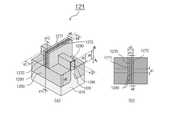
도 1은 종래의 소자 구조(출처: S. Tiwari et al., International Electron Device Meeting, pp. 737-740, 1998)로서 주 게이트(7) 측면에 일함수가 다른 측면 게이트(8)가 바로 붙어있는 SOI (Silicon On Insulator) 구조의 소자로 실리콘 필름(20) 아래에도 주 게이트(7)와 같은 일함수를 갖는 게이트가 있는 이중-게이트 구조의 소자이다. 이 구조에서는 측면 게이트(8)를 스페이서 형태로 구성하기 때문에 실제 게이트 길이가 길어지는 단점이 있다. 특히 SOI 형태의 소자구조이기 때문에 DRAM과 같이 누설전류가 민감한 소자 응용에는 매우 부적합하다. 하부 게이트는 주게이트(7)와 일함수가 같은 물질로 구성된다. 이 구조는 GIDL을 줄이기 위한 것이 아니고, 소자의 짧은채널효과를 억제하고 성능을 높이기 위해 고안된 것이다.1 is a conventional device structure (Source: S. Tiwari et al., International Electron Device Meeting, pp. 737-740, 1998), with the
도 2는 종래의 소자 구조로서 SOI 기판에 구현된 이중-게이트 소자구조 (출처: G. V. Reddy et al., IEEE Trans. on Nanotechnology, vol. 4, no. 2, pp. 260-268, March 2005)를 보이고 있다. 이 구조에서 상부 게이트의 반은 일함수가 큰 주 게이트(7)이고 나머지 반은 일함수가 작은 게이트(8)가 붙어서 형성되어 있고, 하부 게이트는 일함수가 작은 게이트(8)로 구성되어 있다. 상부 게이트는 원래 p+ 다결정실리콘 하나로 구성되었는데, 이 게이트의 반을 n+로 바꾸면서 짧은채널효과를 더 억제할 수 있게 되었다. 이 논문에서도 도 1에서와 같이 SOI 기판을 사용하고 있고, 상부 게이트에는 일함수가 다른 2가지 물질을 사용하고 하부 게이트는 n+ 도우핑된 단일 게이트 구조를 적용하고 있다. 하부 게이트가 n+이기 때문에 문턱전압이 낮고, 따라서 DRAM에는 적용할 수 없다.FIG. 2 shows a double-gate device structure implemented on an SOI substrate as a conventional device structure (Source: GV Reddy et al., IEEE Trans.on Nanotechnology, vol. 4, no. 2, pp. 260-268, March 2005) Is showing. In this structure, half of the upper gate is formed by the
도 3의 (a)는 기존의 소자구조(출처: S. Han et al., IEEE Trans. on Electron Devices, vol. 48, no. 9, pp. 2058-2064, Sep. 2005)로서 일함수가 작은 게이트(8)가 일함수가 큰 주 게이트(7)와 절연막(10)으로 격리되어 형성되어 있다. 게이트(8)는 그 아래의 채널에 쉽게 채널을 유기할 수 있는 특징이 있어, 전기적으로 유기된 반전층이 소자의 LDD (Lightly Doped Drain) 역할을 하도록 했다. 채널의 구조가 평탄채널 구조이므로 기존의 평탄채널 구조가 갖는 문제를 모두 갖고 있다. 또한 GIDL을 줄일 필요성이 없는 구조이며, 이에 대한 언급도 없다.FIG. 3 (a) is a conventional device structure (source: S. Han et al., IEEE Trans.on Electron Devices, vol. 48, no. 9, pp. 2058-2064, Sep. 2005). The
도 3의 (b)는 기존의 소자구조(출처: A. A. Orouji et al., IEEE Trans. on Device and Materials Reliability, vol. 5, no. 3, pp. 509-514, Sep. 2005)로서 이중-게이트 구조를 가지고 있다. 이중-게이트 중 하부 게이트는 n+ 게이트로 되어 있고, 상부 게이트는 주요 게이트인 p+와 주 게이트와 전기적으로 격리된 n+ 측면 게이트로 되어 있다. 이 문헌에서는 상기와 같은 게이트 전극 구조를 도입하여 짧은채널효과 를 개선하고 hot carrier의 생성을 억제를 할 수 있다고 밝히고 있다. SOI 기판에 형성되었기 때문에 SOI 소자가 갖는 문제점을 갖고 있다. 또한 상부 게이트는 일함수가 작은 측면 게이트와 일함수가 큰 주요 게이트가 전기적으로 분리되어 있어 실제 소자제작에서는 소자의 면적이 증가하는 단점이 발생한다.Figure 3 (b) is a conventional device structure (Source: AA Orouji et al., IEEE Trans.on Device and Materials Reliability, vol. 5, no. 3, pp. 509-514, Sep. 2005) It has a gate structure. The lower gate of the double-gate is the n+ gate, and the upper gate is the p+ main gate and the n+ side gate electrically isolated from the main gate. In this document, the gate electrode structure as described above can improve the short channel effect and suppress the generation of hot carrier. Since it is formed in the SOI substrate, there is a problem with the SOI element. In addition, the upper gate is electrically separated from the side gate having a small work function and the main gate having a large work function, thereby increasing the area of the device in actual device fabrication.
전술한 문제점을 해결하기 위한 본 발명의 목적은 축소화 특성이 우수하고 OFF 상태의 누설전류를 최소화시켜 고집적 DRAM 셀로 사용할 수 있도록 한 FinFET을 제공한 것이다.SUMMARY OF THE INVENTION An object of the present invention for solving the above-described problems is to provide a FinFET that can be used as a highly integrated DRAM cell with excellent miniaturization characteristics and minimizing leakage current in the OFF state.
본 발명의 다른 목적은 전체적으로 문턱전압을 상승시키면서 GIDL(Gate Induced Drain Leakage)를 감소시킬 수 있는 구조로 이루어지는 벌크 실리콘 기판을 이용한 FinFET 을 제공하는 것이다.Another object of the present invention is to provide a FinFET using a bulk silicon substrate having a structure capable of reducing a gate induced drain leakage (GIDL) while increasing a threshold voltage as a whole.
본 발명의 또 다른 목적은 전술한 FinFET을 제조하는 방법을 제공하는 것이다.It is yet another object of the present invention to provide a method of manufacturing the FinFET described above.
전술한 기술적 과제를 달성하기 위한 본 발명의 제1 특징에 따른 낮은 누설 전류를 갖는 Fin 전계효과트랜지스터는,Fin field effect transistor having a low leakage current according to the first aspect of the present invention for achieving the above technical problem,
벌크 실리콘 기판, Bulk silicon substrate,
상기 기판을 패터닝하여 형성되며, 소정의 높이와 폭, 및 소정의 길이를 갖는 담장 형태로 이루어지는 담장형 바디,A fence-shaped body formed by patterning the substrate and having a fence shape having a predetermined height and width and a predetermined length;
전기적 절연 물질로 이루어지며, 상기 기판의 표면 및 상기 담장형 바디의 제1 높이까지 형성되는 절연막,An insulating film made of an electrically insulating material, the insulating film being formed up to a first height of the surface of the substrate and the fence body;
상기 절연막위로 돌출된 담장형 바디의 측벽 및 상부 표면에 형성되는 게이트 절연막,A gate insulating film formed on sidewalls and top surfaces of the fence-like body protruding onto the insulating film;
상기 게이트 절연막 및 상기 절연막 위에 형성되되, 상기 담장형 바디의 길이 방향과는 수직 방향으로 형성되는 게이트 전극,A gate electrode formed on the gate insulating film and the insulating film, the gate electrode being formed in a direction perpendicular to a length direction of the fence body;
상기 담장형 바디 중 상기 게이트 전극이 형성되지 않은 영역에 형성되는 소스/드레인 영역을 포함하며,A source / drain region formed in an area in which the gate electrode is not formed in the fence body;
상기 게이트 전극은 제1 게이트 전극 및 상기 제1 게이트 전극과 전기적으로 결합된 제2 게이트 전극으로 이루어지며, 상기 제2 게이트 전극은 제1 게이트 전극의 일함수보다 낮은 일함수를 가지며, 상기 제2 게이트 전극은 상기 제1 게이트 전극의 한쪽 측면에 형성되되 드레인 영역 쪽에 형성된다.The gate electrode includes a first gate electrode and a second gate electrode electrically coupled to the first gate electrode, the second gate electrode having a work function lower than that of the first gate electrode, and the second gate electrode. The gate electrode is formed on one side of the first gate electrode but on the drain region side.
본 발명의 제2 특징에 따른 낮은 누설 전류를 갖는 Fin 전계효과 트랜지스터는,Fin field effect transistor having a low leakage current according to a second aspect of the present invention,
벌크 실리콘 기판,Bulk silicon substrate,
상기 기판을 패터닝하여 형성되며, 소정의 높이와 폭, 및 소정의 길이를 갖 는 담장 형태로 이루어지는 담장형 바디,A fence-shaped body formed by patterning the substrate and having a fence shape having a predetermined height and width and a predetermined length;
전기적 절연 물질로 이루어지며, 상기 기판의 표면 및 상기 담장형 바디의 제1 높이까지 형성되는 절연막,An insulating film made of an electrically insulating material, the insulating film being formed up to a first height of the surface of the substrate and the fence body;
상기 절연막위로 돌출된 담장형 바디의 측벽 및 상부 표면에 형성되는 게이트 절연막,A gate insulating film formed on sidewalls and top surfaces of the fence-like body protruding onto the insulating film;
상기 게이트 절연막 및 상기 절연막 위에 형성되되, 상기 담장형 바디의 길이 방향과는 수직 방향으로 형성되는 게이트 전극,A gate electrode formed on the gate insulating film and the insulating film, the gate electrode being formed in a direction perpendicular to a length direction of the fence body;
상기 담장형 바디 중 상기 게이트 전극이 형성되지 않은 영역에 형성되는 소스/드레인 영역을 포함하며,A source / drain region formed in an area in which the gate electrode is not formed in the fence body;
상기 게이트 전극은 제1 게이트 전극, 상기 제2 게이트 전극 및 상기 제1 게이트 전극과 제2 게이트 전극의 사이에 배치되는 격리용 절연막으로 이루어지며, 상기 제2 게이트 전극은 상기 제1 게이트 전극보다 낮은 일함수를 가지며, 상기 제2 게이트 전극은 상기 격리용 절연막을 개재하여 제1 게이트 전극의 한쪽 측면에 형성되되 드레인 영역 쪽에 형성된다.The gate electrode includes a first insulating film disposed between the first gate electrode, the second gate electrode, and the first gate electrode and the second gate electrode, and the second gate electrode is lower than the first gate electrode. It has a work function, and the second gate electrode is formed on one side of the first gate electrode via the isolation insulating film, but formed on the drain region side.
본 발명의 제3 특징에 따른 낮은 누설전류를 갖는 Fin 전계효과 트랜지스터는,Fin field effect transistor having a low leakage current according to a third aspect of the present invention,
벌크 실리콘 기판,Bulk silicon substrate,
상기 기판을 패터닝하여 형성되며, 소정의 높이와 폭, 및 소정의 길이를 갖는 담장 형태로 이루어지는 담장형 바디,A fence-shaped body formed by patterning the substrate and having a fence shape having a predetermined height and width and a predetermined length;
전기적 절연 물질로 이루어지며, 상기 기판의 표면 및 상기 담장형 바디의 제1 높이까지 형성되는 절연막,An insulating film made of an electrically insulating material, the insulating film being formed up to a first height of the surface of the substrate and the fence body;
상기 절연막위로 돌출된 담장형 바디의 측벽 및 상부 표면에 형성되는 게이트 절연막,A gate insulating film formed on sidewalls and top surfaces of the fence-like body protruding onto the insulating film;
상기 게이트 절연막 및 상기 절연막 위에 형성되되, 상기 담장형 바디의 길이 방향과는 수직 방향으로 형성되는 게이트 전극,A gate electrode formed on the gate insulating film and the insulating film, the gate electrode being formed in a direction perpendicular to a length direction of the fence body;
상기 담장형 바디 중 상기 게이트 전극이 형성되지 않은 영역에 형성되는 소스/드레인 영역을 포함하며,A source / drain region formed in an area in which the gate electrode is not formed in the fence body;
상기 게이트 전극은 제1 게이트 전극 및 상기 제1 게이트 전극의 양측면에 각각 형성되는 제2 게이트 전극들로 이루어지며, 상기 제2 게이트 전극들은 상기 제1 게이트 전극보다 낮은 일함수를 가지며, 상기 제2 게이트 전극은 상기 제1 게이트 전극의 양측면에 각각 형성되되 소오스 및 드레인 영역 쪽에 각각 형성된다.The gate electrode includes a first gate electrode and second gate electrodes formed on both side surfaces of the first gate electrode, and the second gate electrodes have a lower work function than the first gate electrode. Gate electrodes are formed on both sides of the first gate electrode, respectively, and are formed on the source and drain regions, respectively.
본 발명의 제4 특징에 따른 낮은 누설전류를 갖는 Fin 전계효과 트랜지스터는,Fin field effect transistor having a low leakage current according to a fourth aspect of the present invention,
벌크 실리콘 기판,Bulk silicon substrate,
상기 기판을 패터닝하여 형성되며, 소정의 높이와 폭, 및 소정의 길이를 갖는 담장 형태로 이루어지는 담장형 바디,A fence-shaped body formed by patterning the substrate and having a fence shape having a predetermined height and width and a predetermined length;
전기적 절연 물질로 이루어지며, 상기 기판의 표면 및 상기 담장형 바디의 제1 높이까지 형성되는 절연막,An insulating film made of an electrically insulating material, the insulating film being formed up to a first height of the surface of the substrate and the fence body;
상기 절연막위로 돌출된 담장형 바디의 측벽 및 상부 표면에 형성되는 게이트 절연막,A gate insulating film formed on sidewalls and top surfaces of the fence-like body protruding onto the insulating film;
상기 게이트 절연막 및 상기 절연막 위에 형성되되, 상기 담장형 바디의 길이 방향과는 수직 방향으로 형성되는 게이트 전극,A gate electrode formed on the gate insulating film and the insulating film, the gate electrode being formed in a direction perpendicular to a length direction of the fence body;
상기 담장형 바디 중 상기 게이트 전극이 형성되지 않은 영역에 형성되는 소스/드레인 영역을 포함하며,A source / drain region formed in an area in which the gate electrode is not formed in the fence body;
상기 게이트 전극은 제1 게이트 전극, 상기 제1 게이트 전극의 양측면에 각각 형성되는 제2 게이트 전극들, 및 상기 제1 게이트 전극과 상기 제2 게이트 전극의 사이에 배치되는 격리용 절연막들로 이루어지며, 상기 제2 게이트 전극들은 상기 제1 게이트 전극보다 낮은 일함수를 가지며, 상기 제2 게이트 전극들은 상기 제1 게이트 전극의 양측면에 각각 형성되되 소오스 및 드레인 영역 쪽에 각각 형성된다.The gate electrode may include a first gate electrode, second gate electrodes formed on both sides of the first gate electrode, and insulating insulating layers disposed between the first gate electrode and the second gate electrode. The second gate electrodes have a lower work function than the first gate electrode, and the second gate electrodes are formed on both sides of the first gate electrode, respectively, and are formed on the source and drain regions, respectively.
전술한 제1, 제2, 제3 및 제4 특징을 갖는 Fin 전계효과 트랜지스터의 상기 절연막은, 상기 기판과 상기 담장형 바디의 측면에 형성되는 열산화막, 및 상기 열산화막위에 증착되어 해당 소자를 인접한 소자와 전기적으로 분리시키는 소자 격리막을 포함할 수 있다.The insulating film of the Fin field effect transistor having the first, second, third and fourth characteristics described above is deposited on the thermal oxide film formed on the side surface of the substrate and the fence body, and the thermal oxide film is used to form the device. It may include a device isolation layer to electrically separate from the adjacent device.
전술한 제1, 제2, 제3 및 제4 특징을 갖는 Fin 전계효과 트랜지스터의 상기 절연막은, 상기 기판과 상기 담장형 바디의 측면에 형성되는 열산화막, 상기 열산화막위에 형성되는 질화막, 및 상기 질화막의 상부에 증착되어 해당 소자를 인접한 소자와 전기적으로 분리시키는 소자 격리막을 포함할 수도 있다.The insulating film of the Fin field effect transistor having the above-described first, second, third and fourth characteristics may include a thermal oxide film formed on the side surface of the substrate and the fence body, a nitride film formed on the thermal oxide film, and the It may also include a device isolation layer deposited on top of the nitride film to electrically isolate the device from adjacent devices.
전술한 제1, 제2, 제3 및 제4 특징을 갖는 Fin 전계효과 트랜지스터에 있어서, 상기 담장형 바디의 상부 표면의 모서리 부분은 원형으로 이루어지며,In the Fin field effect transistor having the above-mentioned first, second, third and fourth features, the corner portion of the upper surface of the fence body is circular,
상기 담장형 바디의 폭은 수직방향으로 전체적으로 균일하거나, 담장형 바디의 상부 표면으로부터 기판으로 갈수록 점차 넓어지거나, 상부 표면으로부터 상기 제1 높이 근처까지 균일한 폭으로 형성되고 제1 높이부터 기판까지 점차 넓어지도록 형성하며,The width of the fenced body is generally uniform in the vertical direction, or gradually widens from the top surface of the fenced body to the substrate, or is formed with a uniform width from the top surface to near the first height and gradually from the first height to the substrate. To broaden,
상기 담장형 바디의 측면에 형성되는 측면 채널의 높이는 2 nm ~ 200 nm 사이의 범위에서 결정되는 것이 바람직하다.The height of the side channels formed on the side of the fence-like body is preferably determined in the range between 2 nm and 200 nm.
전술한 제1, 제2, 제3 및 제4 특징을 갖는 Fin 전계효과 트랜지스터에 있어서, 상기 게이트 절연막 중 상기 담장형 바디의 측면에 형성되는 게이트 절연막의 두께는 0.5 nm ~ 10 nm 이며, 상기 담장형 바디의 상부 표면에 형성되는 게이트 절연막의 두께는 0.5 nm ~ 200 nm 로 형성하는 것이 바람직하며,In the Fin field effect transistor having the first, second, third and fourth features described above, the thickness of the gate insulating film formed on the side of the fence-type body of the gate insulating film is 0.5 nm to 10 nm, the fence The thickness of the gate insulating film formed on the upper surface of the type body is preferably formed to be 0.5 nm ~ 200 nm,
상기 담장형 바디의 측면 및 상부에 형성되는 게이트 절연막의 두께는 채널의 안쪽에서는 0.5 nm ~ 200 nm 이며, 소스/드레인 쪽으로 갈수록 절연막의 두께를 점차 두껍게 하되 최종적으로 0.6 nm ~ 201 nm 인 것이 바람직하다.The thickness of the gate insulating film formed on the side and the top of the fence-shaped body is 0.5 nm to 200 nm in the inner side of the channel, and the thickness of the insulating film is gradually increased toward the source / drain, but it is preferably 0.6 nm to 201 nm. .
전술한 제1, 제2, 제3 및 제4 특징을 갖는 Fin 전계효과 트랜지스터에 있어서, 상기 소스/드레인 영역의 깊이는 담장형 바디의 상부 표면으로부터 10 nm ~ 500 nm 인 것이 바람직하다. In the Fin field effect transistor having the above-mentioned first, second, third and fourth features, the depth of the source / drain region is preferably 10 nm to 500 nm from the upper surface of the fence body.
전술한 제1, 제2, 제3 및 제4 특징을 갖는 Fin 전계효과 트랜지스터에 있어서, 담장형 바디의 폭은 채널길이방향으로 균일하게 형성되도록 하거나, 또는 게이트 전극과 교차하는 영역을 제외한 소스/드레인이 형성되는 영역의 담장형 바디의 폭은 게이트 전극과 교차하는 영역의 담장형 바디의 폭 보다 넓거나 좁게 형성할 수 있다. 특히, 소스/드레인이 형성되는 영역의 담장형 바디의 폭을 게이트 전극과 교차되는 영역의 담장형 바디의 폭보다 넓게 형성한 경우, 소스/드레인 저항을 줄일 수 있다.In the Fin field effect transistor having the above-mentioned first, second, third and fourth features, the width of the fence body is formed to be uniform in the channel length direction, or the source / except an area crossing the gate electrode. The width of the fenced body of the region where the drain is formed may be wider or narrower than the width of the fenced body of the region crossing the gate electrode. In particular, when the width of the fenced body of the region where the source / drain is formed is wider than the width of the fenced body of the region that intersects the gate electrode, the source / drain resistance can be reduced.
전술한 제1, 제2, 제3 및 제4 특징을 갖는 Fin 전계효과 트랜지스터에 있어서, 제1 게이트 전극 및 제2 게이트 전극은 서로 같은 물질로 구성하되 불순물 도우핑 유형을 바꾸거나, 서로 다른 물질로 구성하거나, 서로 다른 물질로 구성하고 불순물 도우핑 유형을 바꾸어서, 제1 게이트 전극 및 제2 게이트 전극의 일함수가 서로 다르게 하는 것이 바람직하며,In the Fin field effect transistor having the above-described first, second, third and fourth characteristics, the first gate electrode and the second gate electrode may be made of the same material, but the impurity doping type may be changed or different materials may be used. It is preferable that the work function of the first gate electrode and the second gate electrode is different from each other, or by using different materials and changing the type of impurity doping.
상기 게이트 전극은 다결정 실리콘, 다결정 SiGe, 다결정 Ge, 비정질 실리콘, 비정질 SiGe, 비정질Ge, 실리콘, 또는 반도체 재료와 금속과의 실리사이드, 각종 금속산화물, 다양한 일함수의 금속, TaN, TiN, WN와 같은 이원계 금속 중 적어도 하나 이상으로 이루어질 수 있다.The gate electrode may be polycrystalline silicon, polycrystalline SiGe, polycrystalline Ge, amorphous silicon, amorphous SiGe, amorphous Ge, silicon, or silicides of semiconductor materials and metals, various metal oxides, metals of various work functions, such as TaN, TiN, WN It may be made of at least one of binary metals.
본 발명의 제5 특징에 따른 Fin 전계효과트랜지스터 제조 방법은,Fin field effect transistor manufacturing method according to a fifth aspect of the present invention,
(a) 벌크 실리콘 기판에 단결정 실리콘으로 담장형 바디를 형성하는 단계,(a) forming a fenced body of monocrystalline silicon on a bulk silicon substrate,
(b) 상기 벌크 실리콘 기판의 표면에서 담장형 바디의 제1 높이까지 절연막을 형성하는 단계,(b) forming an insulating film from the surface of the bulk silicon substrate to a first height of the fenced body,
(c) 상기 제1 높이 이상의 담장형 바디의 측면 및 상부 표면에 게이트 절연막을 형성하는 단계,(c) forming a gate insulating film on side surfaces and top surfaces of the fence-shaped body of the first height or more,
(d) 상기 절연막 및 상기 게이트 절연막 위에 게이트 전극을 형성하되, 상기 게이트 전극은 일함수가 서로 다른 제1 게이트 전극과 제2 게이트 전극으로 이루어 지는 것을 특징으로 하는 단계,(d) forming a gate electrode on the insulating film and the gate insulating film, wherein the gate electrode is formed of a first gate electrode and a second gate electrode having different work functions;
(e) 상기 담장형 바디 중 상기 게이트 전극이 덮고 있는 영역을 제외한 나머지 영역에 소스/드레인 영역을 형성하는 단계를 포함한다.(e) forming a source / drain region in the remaining region of the fenced body except for the region covered by the gate electrode.
전술한 제5 특징에 따른 FinFET 제조방법의 상기 (b) 절연막 형성 단계는The (b) insulating film forming step of the FinFET manufacturing method according to the fifth feature described above
(b1) 상기 벌크 실리콘 기판의 표면 및 상기 담장형 바디의 표면을 열산화시켜 제1 절연막을 형성하는 단계, 및(b1) thermally oxidizing the surface of the bulk silicon substrate and the surface of the fence body to form a first insulating film, and
(b2) 상기 제1 절연막위에 제2 절연막을 형성하는 단계;(b2) forming a second insulating film on the first insulating film;
(b3) 상기 제2 절연막 및 제1 절연막을 상기 담장형 바디의 제1 높이까지 선택적 식각하는 단계를 구비한다.(b3) selectively etching the second insulating film and the first insulating film to a first height of the fence-type body.
전술한 제5 특징에 따른 FinFET 제조방법의 상기 (b) 절연막 형성 단계는The (b) insulating film forming step of the FinFET manufacturing method according to the fifth feature described above
(b1) 상기 벌크 실리콘 기판의 표면 및 상기 담장형 바디의 표면을 열산화시켜 제1 절연막을 형성하는 단계;(b1) thermally oxidizing a surface of the bulk silicon substrate and a surface of the fenced body to form a first insulating film;
(b2) 상기 제1 절연막위에 질화막을 형성하는 단계;(b2) forming a nitride film on the first insulating film;
(b3) 상기 질화막위에 제2 절연막을 형성하는 단계; 및(b3) forming a second insulating film on the nitride film; And
(b4) 상기 질화막 및 제2 절연막을 상기 담장형 바디의 제1 높이까지 선택적 식각하는 단계를 구비한다.(b4) selectively etching the nitride film and the second insulating film to a first height of the fence-type body.
전술한 제5 특징에 따른 FinFET 제조방법의 상기 (d) 게이트 전극 형성 단계는, 상기 절연막 및 상기 게이트 절연막 위에 게이트 전극을 형성하되, 상기 게이트 전극은 제1 게이트 전극 및 상기 제1 게이트 전극의 드레인 방향 측면에 연결되는 제2 게이트 전극으로 이루어지며, 상기 제2 게이트 전극은 상기 제1 게이트 전극보다 일함수가 작은 것이 바람직하다. In the forming of the (d) gate electrode of the FinFET manufacturing method according to the fifth aspect, a gate electrode is formed on the insulating film and the gate insulating film, wherein the gate electrode is a drain of the first gate electrode and the first gate electrode. It is preferably made of a second gate electrode connected to the lateral side, the second gate electrode is preferably less work function than the first gate electrode.
전술한 제5 특징에 따른 FinFET 제조방법의 (a) 담장형 바디 형성 단계는,(A) The fence body forming step of the FinFET manufacturing method according to the fifth feature described above,
(a1) 실리콘 기판에 마스크 물질로서 산화막이나 질화막 또는 산화막과 질화막을 형성하는 단계,(a1) forming an oxide film, a nitride film, or an oxide film and a nitride film as a mask material on a silicon substrate,
(a2) 상기 마스크 물질을 패터닝하여 담장형 바디용 마스크를 형성하는 단계,(a2) patterning the mask material to form a mask for the fence body;
(a3) 상기 담장형 바디용 마스크를 이용하여 상기 실리콘 기판을 식각하여 담장형 바디를 형성하는 단계를 포함하는 것이 바람직하다.(a3) Preferably, the silicon substrate is etched using the mask for the fenced body to form a fenced body.
전술한 제5 특징에 따른 FinFET 제조방법의 상기 (c) 게이트 절연막 형성단계는, 상기 제1 높이 이상의 노출된 담장형 바디의 상부 표면 및 측면에 균일한 두께로 게이트 산화막을 형성하거나, 결정 방향성을 고려한 산화막 성장을 수행하여 측면의 (110) 방향이 상대적으로 상부 표면에서 보다 더 두껍게 산화막이 성장되도록 하거나, 담장형 바디의 상부 표면에 형성되는 게이트 절연막의 두께가 담장형 바디의 측면에 형성되는 게이트 절연막의 두께보다 두껍게 형성되도록 할 수 있다. In the forming of the (c) gate insulating film of the FinFET manufacturing method according to the fifth aspect, the gate oxide film may be formed to have a uniform thickness on the upper surface and the side surface of the exposed fenced body having the first height or more, By considering the oxide film growth, the oxide film is grown to be thicker than the upper surface of the (110) direction, or the gate insulating film formed on the upper surface of the fence body is formed on the side of the fence body. It can be made thicker than the thickness of the insulating film.
전술한 제5 특징에 따른 FinFET 제조방법의 상기 (b) 절연막 형성 단계, 및 (c) 게이트 절연막 형성 단계는,The (b) insulating film forming step and (c) the gate insulating film forming step of the FinFET manufacturing method according to the fifth feature described above,
담장형 바디를 형성하기 위해 초기에 기판 표면에 형성된 담장형 바디용 하드(hard) 마스크를 담장형 바디의 상부에 남도록 하는 단계, Leaving a hard mask for the fenced body initially formed on the substrate surface to form the fenced body, on top of the fenced body,
제1 절연막, 질화막 및 제 2절연막을 순차적으로 형성하는 단계,Sequentially forming the first insulating film, the nitride film, and the second insulating film,
상기 담장형 바디의 상부에 형성된 질화막의 표면 근처까지 평탄화하는 단 계,Planarizing to near the surface of the nitride film formed on the upper portion of the fence-like body,
담장형 바디의 상부 표면으로부터 제1 깊이까지 상기 질화막을 선택적으로 식각하는 단계,Selectively etching the nitride film from a top surface of the fenced body to a first depth,
노출된 담장형 바디의 측면의 제 1절연막을 식각하여 담장형 바디의 측면이 드러나게 하는 단계,Etching the first insulating layer on the side of the exposed fenced body to expose the side of the fenced body;
담장형 바디의 측면이 노출된 상태에서 어닐링하는 단계,Annealing with the side of the fenced body exposed;
노출된 담장형 바디의 상부 표면 및 측면에 게이트 절연막을 형성하되 담장형 바디의 상부 표면에 남아있는 절연막의 두께보다 얇게 형성하는 단계,Forming a gate insulating film on an upper surface and a side surface of the exposed fenced body but having a thickness smaller than the thickness of the insulating film remaining on the upper surface of the fenced body;
를 포함하여 담장형 바디의 상부 표면에 형성된 게이트 절연막의 두께가 담장형 바디의 측면에 형성된 게이트 절연막의 두께보다 두껍게 형성되도록 하는 것이 바람직하다.It is preferable that the thickness of the gate insulating film formed on the upper surface of the fence-like body including a thicker than the thickness of the gate insulating film formed on the side of the fence-like body.
전술한 제5 특징에 따른 FinFET 제조방법의 상기 (d) 게이트 전극 형성 단계는,The (d) gate electrode forming step of the FinFET manufacturing method according to the fifth feature described above,
(d1) 게이트 절연막위에 게이트 전극 형성을 위한 다결정 실리콘막을 형성하는 단계와,(d1) forming a polycrystalline silicon film for forming a gate electrode on the gate insulating film;
(d2) 다결정 실리콘막을 고농도의 p+로 도우핑하는 단계와,(d2) doping the polycrystalline silicon film with a high concentration of p+ , and
(d3) 도우핑된 다결정 실리콘막 위에 일정 두께의 절연막을 형성하는 단계와,(d3) forming an insulating film having a predetermined thickness on the doped polycrystalline silicon film;
(d4) 사진식각공정을 이용하여 상기 절연막 및 상기 다결정 실리콘막을 식각 하여 패터닝하는 단계와,(d4) etching and patterning the insulating film and the polycrystalline silicon film using a photolithography process;
(d5) 상기 p+ 도핑된 다결정 실리콘막의 측면을 n+로 카운터 도우핑하는 단계를 포함하는 것이 바람직하다.and (d5) counter-doping the side of the p+ doped polycrystalline silicon film with n+ .
전술한 제5 특징에 따른 FinFET 제조방법의 상기 (d) 게이트 전극 형성 단계는,The (d) gate electrode forming step of the FinFET manufacturing method according to the fifth feature described above,
(d1) 게이트 전극 형성을 위한 다결정 실리콘막을 게이트 절연막위에 형성하는 단계,(d1) forming a polycrystalline silicon film on the gate insulating film for forming a gate electrode,
(d2) 다결정 실리콘막을 고농도의 p+로 도우핑하는 단계,(d2) doping the polycrystalline silicon film with a high concentration of p+ ,
(d3) 도우핑된 다결정 실리콘막위에 일정 두께의 절연막을 형성하는 단계,(d3) forming an insulating film having a predetermined thickness on the doped polycrystalline silicon film,
(d3) 게이트 전극용 마스크를 이용하여 상기 절연막 및 상기 다결정 실리콘막을 식각하여 패터닝하는 단계,(d3) etching and patterning the insulating film and the polycrystalline silicon film using a mask for a gate electrode,
(d4) 얇은 두께의 질화막을 증착하고 비등방 식각하여 질화막 스페이서를 형성하여 다결정실리콘막의 측면을 가리는 단계,(d4) depositing a thin film of nitride and anisotropically etching to form a nitride film spacer to cover the side of the polysilicon film;
(d5) 소스/드레인 영역에 일정 두께의 산화막을 성장하는 단계,(d5) growing an oxide film having a predetermined thickness in the source / drain region,
(d6) 상기 질화막 스페이서를 제거하여 p+ 다결정 실리콘의 측면이 드러나게 하는 단계,(d6) removing the nitride film spacers so that the side surface of p+ polycrystalline silicon is exposed;
(d7) 다결정 실리콘 위에 형성된 절연막의 중심을 기준으로 소스 영역을 포토리지스트로 가리는 단계,(d7) covering the source region with a photoresist based on the center of the insulating film formed on the polycrystalline silicon,
(d8) 노출된 p+ 다결정 실리콘의 측면을 n+로 카운터 도우핑하는 단계를 포함하는 것이 바람직하다.(d8) preferably counter-doping the side of the exposed p+ polycrystalline silicon to n+ .
전술한 제5 특징에 따른 FinFET 제조방법의 상기 (e) 소스/드레인 영역 형성 단계는,The (e) source / drain region forming step of the method of manufacturing a FinFET according to the fifth feature described above is
(e1) 게이트 전극 형성된 후, LDD (Lightly Doped Drain)를 형성하기 위한 이온주입이나 플라즈마 도우핑을 수행하거나, 일정 두께의 절연막을 스페이서로 형성한 후 LDD를 형성하기 위한 이온주입이나 플라즈마 도우핑을 수행하는 단계와,(e1) After the gate electrode is formed, ion implantation or plasma doping is performed to form a lightly doped drain (LDD), or an ion implantation or plasma doping to form an LDD is performed after forming an insulating film having a predetermined thickness as a spacer. Performing steps,
(e2) 절연막을 이용한 스페이서를 형성하는 단계와,(e2) forming a spacer using an insulating film,
(e3) 이온주입이나 플라즈마 도우핑을 수행하여 n+ HDD (Heavily Doped Drain) 소스/드레인을 형성하는 단계를 포함하는 것이 바람직하다.(e3) preferably, performing ion implantation or plasma doping to form n+ HDD (Heavily Doped Drain) source / drain.
본 발명의 제6 특징에 따른 FinFET 제조 방법은FinFET manufacturing method according to a sixth aspect of the present invention
(a) 벌크 실리콘 기판에 단결정 실리콘으로 이루어진 담장형 바디를 형성하는 단계와,(a) forming a fenced body of monocrystalline silicon on a bulk silicon substrate,
(b) 상기 벌크 실리콘 기판의 표면에서 담장형 바디의 상부 표면 근처까지 제 1절연막 및 제 2절연막을 순차적으로 형성하는 단계와,(b) sequentially forming a first insulating film and a second insulating film from the surface of the bulk silicon substrate to near the upper surface of the fence body;
(c) 상기 담장형 바디의 표면에 제 3절연막을 형성하는 단계와,(c) forming a third insulating film on the surface of the fence body;
(d) 상기 제 3절연막 위에 선택적 식각성이 있는 제 4절연막 또는 반도체막을 형성하는 단계와,(d) forming a fourth insulating film or a semiconductor film with selective etching on the third insulating film;
(e) 게이트를 열어주는 마스크를 이용하여 포토리지스트 패턴을 형성하는 단 계와,(e) forming a photoresist pattern using a mask that opens the gate;
(f) 상기 패턴을 이용하여 상기 제 4 절연막 또는 반도체 막을 식각하고 순차적으로 제 3절연막을 식각하는 단계와,(f) etching the fourth insulating film or the semiconductor film using the pattern and sequentially etching the third insulating film;
(g) 상기 제 1, 2 절연막을 바디의 표면에서 일정 깊이까지 수직으로 식각하는 단계와,(g) etching the first and second insulating films vertically from the surface of the body to a predetermined depth;
(h) 상기 포토리지스트 패턴을 제거하는 단계와,(h) removing the photoresist pattern;
(i) 상기 노출된 담장형 바디의 표면 및 일부 측면에 희생 산화막을 성장하는 단계와,(i) growing a sacrificial oxide film on the surface and some side surfaces of the exposed fenced body,
(j) 채널 이온주입을 하고 어닐링을 수행하는 단계와,(j) performing channel ion implantation and annealing,
(k) 상기 희생 산화막을 제거하고 표면특성 개선을 위한 어닐링 단계와,(k) annealing to remove the sacrificial oxide and improve surface properties;
(l) 게이트 절연막을 형성하는 단계와,(l) forming a gate insulating film;
(m) 게이트 전극을 위한 다결정실리콘막을 증착하는 단계와,(m) depositing a polysilicon film for the gate electrode,
(n) 상기 게이트 전극을 p+ 도우핑하고 어닐링하는 단계와,(n) p+ doping and annealing the gate electrode;
(o) 상기 게이트를 열어준 영역에만 p+로 도우핑된 게이트를 남기되 상기 제4 절연막 또는 반도체막의 표면 근처의 아래에만 남기는 단계와,(o) leaving a gate doped with p + only in a region where the gate is opened, but only below the surface of the fourth insulating film or the semiconductor film;
(p) 상기 제 4절연막 또는 반도체 막을 제거하는 단계와,(p) removing the fourth insulating film or the semiconductor film;
(q) 상기 제 1, 2 절연막을 담장형 바디의 표면에서 일정 깊이로 식각하여 게이트 전극의 측면을 노출시키는 단계와,(q) etching the first and second insulating films to a predetermined depth on the surface of the fence body to expose side surfaces of the gate electrode;
(r) 드레인 방향에 있는 게이트 전극의 측벽만 n+로 카운터 도우핑하는 단계 와,(r) counter-doping only the sidewalls of the gate electrodes in the drain direction with n+ ,
(s) 담장형 바디 중 상기 게이트 전극이 덮고 있는 영역 외의 나머지 영역에 소스/드레인 영역을 형성하는 단계를 포함하여 낮은 누설 전류를 갖는 FinFET을 제조할 수 있게 된다.(s) forming a source / drain region in the remaining region of the fenced body other than the region covered by the gate electrode, thereby manufacturing a FinFET having a low leakage current.
바람직한 제1 실시예First preferred embodiment
이하, 첨부된 도면을 참조하여 본 발명의 바람직한 제1 실시예에 따른 낮은 누설 전류를 갖는 FinFET의 구조 및 그 제조 방법을 구체적으로 설명한다.Hereinafter, a structure of a FinFET having a low leakage current and a method of manufacturing the same will be described in detail with reference to the accompanying drawings.
도 4는 본 발명의 바람직한 제1 실시예에 따른 낮은 누설 전류를 갖는 Fin 전계효과트랜지스터를 도시한 도면으로서, 설명과 이해의 편의를 위해 FinFET 소자의 배선을 위한 금속층, 콘택 및 절연층은 제외하고 주요 부분만을 도시하였다. 도 4의 (a)는 본 발명의 바람직한 제1 실시예에 따른 FinFET에 대한 사시도이며, (b)는 평면도이며, (c)는 A-A'방향에 따른 단면도이다.4 is a view showing a fin field effect transistor having a low leakage current according to the first embodiment of the present invention, except for the metal layer, contact and insulating layer for the wiring of the FinFET device for convenience of description and understanding. Only the main part is shown. 4A is a perspective view of a FinFET according to a first preferred embodiment of the present invention, (b) is a plan view, and (c) is a cross-sectional view along the A-A 'direction.
본 발명의 제1 실시예에 따른 FinFET(40)은 기판(410), 담장형 바디(420), 소자 격리막(450), 게이트 절연막(460), 제1 게이트 전극(470), 제2 게이트 전극(480), 소스/드레인 영역(490, 492)을 포함한다.
상기 기판(410)은 벌크 실리콘 기판을 사용한다.The
상기 담장형 바디(420)는 상기 기판(410)위에 형성되며, d1은 담장형 바디의 폭을 나타내는 것으로 2 nm ~ 200 nm 사이의 범위에서 그 폭이 결정된다. d7은 담장형 바디(420)의 전체 높이로서, 50 nm ~ 900 nm 사이의 범위에서 결정된다. d2는 소자 격리막(450) 위로 돌출된 담장형 바디의 높이를 나타내는 것으로서, 2 nm ~ 200 nm 사이의 범위에서 그 높이가 결정되는데, 이 높이는 결국 담장형 바디(420)의 측면에 형성되는 채널의 높이가 된다. 한편, 도 4의 (a)에서는 편의상 담장형 바디(420)의 상부면의 코너를 90 °로 표시하였지만 예각 또는 둔각으로도 형성할 수 있고, 또한 코너를 둥글게 하거나 또는 상부 모양을 반원 모양으로 다양하게 형성할 수 있다.The
상기 게이트 절연막(460)은 상기 담장형 바디(420)의 측면 및 상부 표면에 소정의 두께로 형성되는 게이트 산화막이다. 상기 게이트 절연막(460)에 있어서, 담장형 바디(420)의 측면에 형성되는 게이트 절연막은 0.5 nm ~ 10 nm 사이의 두께로 형성되고, 담장형 바디(420)의 상부 표면에 형성되는 게이트 절연막은 0.5 nm ~ 200 nm 사이의 두께로 형성한다. 이때, 담장형 바디의 상부 표면 및 측면에 형성되는 게이트 절연막(460)의 두께는 전체적으로 균일하게 형성할 수도 있으며, 상부 표면과 측면의 두께를 서로 다르게 형성할 수도 있다.The
특히, 담장형 바디(420)의 상부 표면에 형성되는 게이트 절연막(460)에 있어서, 채널의 안쪽 영역에 해당하는 게이트 절연막은 0.5 ~ 200 nm 사이의 두께(d8)로 형성하고 소스/드레인 영역쪽으로 갈수록 점차 두껍게 하되 최종적으로 0.6 nm ~ 201 nm 사이의 두께(d9)가 되도록 한다.In particular, in the
본 발명의 제1 실시예에 따른 FinFET의 게이트 전극은 일함수가 서로 다른 제1 게이트 전극(470) 및 제2 게이트 전극(480)으로 이루어지며, 상기 제1 게이트 전극(470)과 제2 게이트 전극(480)은 서로 전기적으로 접촉하여 형성되고, d3는 제1 게이트 전극 및 제2 게이트 전극의 전체 길이를 나타낸다.The gate electrode of the FinFET according to the first embodiment of the present invention comprises a
제1 게이트 전극(470)은 소오스 측에 있는 게이트 전극으로서, 일함수가 큰 물질로 형성된다. 따라서, 본 발명에 따른 FinFET 소자의 문턱 전압은 일함수가 큰 제1 게이트 전극(470)에 의하여 주로 결정된다. 한편, 제2 게이트 전극(480)은 드레인 측에 있는 게이트 전극으로서, 제1 게이트 전극(470)보다 낮은 일함수를 가지며, 그 길이(d4)는 전체 게이트 전극의 길이(d3)의 1/2 보다 작고 0.1 nm보다 큰 범위에서 결정된다.The
상기 제1 게이트 전극(470)과 제2 게이트 전극(480)은 서로 같은 물질로 구성하되 불순물 도우핑의 유형을 바꾸어 제2 게이트 전극(480)의 일함수를 작게 할 수도 있으며, 제1 게이트 전극(470)과 제2 게이트 전극(480)의 물질을 서로 다르게 하여 제2 게이트 전극(480)의 일함수를 작게 할 수 있다. 또한, 본 발명에 따른 게이트 전극의 다른 실시 형태는 제1 게이트 전극(470)과 제2 게이트 전극(480)의 물질 및 불순물 도우핑 유형을 모두 달리하여 제2 게이트 전극(480)의 일함수를 제1 게이트 전극(470)의 일함수보다 작게 할 수도 있다.The
제1 게이트 전극(470)과 제2 게이트 전극(480)은 다결정 실리콘, 다결정 SiGe, 다결정 Ge, 비정질 실리콘, 비정질 SiGe, 비정질Ge, 실리콘이나 Ge 같은 반도체 재료를 사용하거나, 다양한 금속과의 실리사이드, 각종 금속산화물, 다양한 일함수의 금속, TaN, TiN, WN와 같은 이원계 금속 등을 사용할 수 있다.The
소자 격리막(450)은 소자 격리 산화막 또는 필드 산화막이라고도 불리어지는데, 담장형 바디(420)의 측면에 형성되어, 해당 소자가 인접한 소자와 전기적으로 격리(isolation)시키게 된다. 상기 소자 격리막(450)의 두께는 d5로 표시되어 있으 며, d5는 50 nm ~ 700 nm의 범위에서 결정된다. 본 발명의 제1 실시예에 따른 소자 격리막(450)은 제1 절연막 및 제2 절연막으로 구성될 수 있으며, 상기 제1 절연막은 상기 담장형 바디가 형성된 실리콘 기판의 표면 및 담장형 바디의 표면을 열산화시켜 형성된 열산화막으로 이루어지며, 제2 절연막은 상기 열산화막위에 산화막을 증착시켜 형성할 수 있게 된다.The
소오스/드레인 영역(490, 492)는 담장형 바디(420)의 소정의 영역에 형성되되, 담장형 바디 중 제1 게이트 전극(470)및 제2 게이트 전극(480)이 형성된 영역의 양 측에 형성된다. 이때, 상기 소오스/드레인 영역의 일부는 상기 제1 게이트 전극 및 제2 게이트 전극의 일부와 겹칠 수도 있으며, 겹치지 않을 수도 있다.The source /
상기 소오스/드레인 영역(490, 492)의 깊이(d6)는 담장형 바디의 표면에서 수직방향으로 정의되며, d6는 5 nm ~ 500 nm의 범위에서 결정된다. 또한, 상기 소오스/드레인(490, 492)이 게이트 전극(470, 480)과 겹치게 되는 경우, 그 길이는 0.1nm ~ 30 nm 의 사이에서 결정된다.The depth d6 of the source /
담장형 바디(420)와 기판(410)이 만나는 부분('B')의 코너는 직각 또는 둥글게 형성될 수 있다.The corner of the portion 'B' where the
도 4에서는 도시되어 있지 않지만, FinFET 소자의 배선을 위해서는 콘택 영역이 소스/드레인 및 게이트 전극에 각각 형성되어야 한다. 소자의 집적도를 개선하고 콘택 저항을 줄이기 위해 금속 층과 접촉하도록 하는 콘택 영역의 크기는 담장형 바디(420)의 폭과 유사하거나 더 크게 형성할 수 있고, 콘택이 더 크게 형성된 경우에는 소오스/드레인 영역(490)이 형성된 담장형 바디의 상부 표면 및 측면 일부에도 콘택이 되도록 할 수 있다.Although not shown in FIG. 4, contact regions must be formed in the source / drain and gate electrodes, respectively, for the wiring of the FinFET device. The size of the contact area, which makes it in contact with the metal layer to improve the device's integration density and reduce the contact resistance, may be similar to or larger than the width of the
소오스/드레인 영역(490)이 형성되는 담장형 바디의 폭을 제1 및 제2 게이트 근처의 채널이 형성되는 담장형 바디의 폭 보다 크게 형성하여 소오스/드레인 영역의 저항을 줄일 수 있다. 본 발명에 따른 FinFET 소자에서는 제2 게이트 전극(480)의 일함수를 작게 함으로써, 제2 게이트 전극과 겹치는 드레인 영역에서 게이트로부터 담장형 바디 방향으로의 전계를 줄이는 것은 물론이고 드레인 바이어스에 의한 수평전계도 줄이는 효과를 가져온다. 그 결과, 본 발명의 목적인 GIDL이 감소하게 되고, 부가적으로 드레인 전압에 의한 전계를 줄임으로써, 핫 캐리어(hot carrier) 발생도 억제할 수 있기 때문에, 소자의 내구성도 개선할 수 있다.The width of the fenced body in which the source /
도 4의 (c)는 도 4의 (a)의 A-A'를 따라 절개하여 도시한 단면도이다. 도 4의 (c)를 통해, 게이트 절연막(460)의 두께 프로파일을 볼 수 있다. 제2 게이트 전극(480)와 드레인 영역이 겹치는 영역에 있어서, 게이트 절연막(460)의 두께(d9)가 채널에서 드레인 영역(492)으로 가면서 두껍게 형성되도록 하여 GIDL (Gate Induced Drain Leakage)을 줄이도록 한다. 여기서, 채널 영역의 게이트 절연막의 두께(d8)는 0.5 nm ~ 200 nm 범위에서 결정되는데 비해, 제2 게이트와 드레인이 겹치는 영역에서의 게이트 절연막의 두께(d9)는 0.6 nm ~ 201 nm의 범위에서 결정되도록 한다. 본 발명의 다른 실시형태에서는, 채널이 형성되는 담장형 바디에 비해 소오스/드레인 영역이 형성되는 담장형 바디의 두께를 더 얇게 형성할 수 있다.FIG. 4C is a cross-sectional view taken along the line AA ′ of FIG. 4A. 4C, the thickness profile of the
이하, 도 5 및 도 6을 참조하여 전술한 구성을 갖는 낮은 누설전류를 갖는 FinFET의 제조 과정을 구체적으로 설명한다. 도 5를 참조하면, 본 발명에 따른 FinFET을 제조하는 과정은, 벌크 실리콘 기판(410)에 단결정 실리콘으로 담장형 바디(420)를 형성하는 단계(단계 500), 상기 벌크 실리콘 기판의 표면에서 담장형 바디의 일정 높이까지 제 1절연막 및 제 2절연막을 형성하는 단계(단계 510), 상기 제1 절연막 및 제2 절연막 위로 돌출된 담장형 바디의 측면 및 상부에 게이트 절연막을 형성하는 단계(단계 520), 상기 제 1, 2절연막이나 게이트 절연막 위에 게이트를 형성하되 일함수가 큰 게이트 물질과 일함수가 작은 게이트 물질로 된 게이트 전극으로 형성하는 단계(단계 530), 상기 게이트 전극이 덮고 있는 담장형 바디를 제외한 담장형 바디에 소오스/드레인 영역을 형성하는 단계(단계 540), 상기 제 1, 2절연막, 게이트 절연막 및 게이트 전극 위에 금속층과의 전기적 격리를 위한 절연막을 형성하는 단계(단계 550), 상기 소오스, 드레인, 게이트에 콘택을 형성하고 배선을 위한 금속층을 형성하는 단계(단계 560)를 포함하고, 이후의 단계는 기존의 단계를 따른다. 이하 전술한 각 단계에 대하여 구체적으로 설명한다.Hereinafter, a manufacturing process of a FinFET having a low leakage current having the above-described configuration will be described in detail with reference to FIGS. 5 and 6. Referring to FIG. 5, a process of manufacturing a FinFET according to the present invention may include forming a
도 6의 (a)는 벌크 실리콘 기판(410)위에 담장형 바디(420)를 형성하는 단계(단계 500)에 의해 형성된 중간 상태의 단면도이다. 담장형 바디 형성 단계(단계 500)는, 실리콘 기판에 하드(hard) 마스크 물질로 사용될 절연막(예:산화막, 질화막, 또는 산화막과 질화막)을 형성하는 단계(단계 502)과, 상기 하드마스크용 절연막을 패터닝하여 담장형 바디를 정의하기 위한 액티브 마스크를 형성히는 단계(단계 503)와, 상기 액티브 마스크를 이용하여 실리콘 기판을 식각하여 담장형 바디를 형성하는 식각단계(단계 504)와, 담장형 바디의 표면을 개선하고, 바디의 폭을 제어하거나 바디의 상부 코너를 둥글게 하기 위하여 적어도 1회이상 산화막을 성장 및 제거하거나 수소 어닐하는 단계(단계 505)와, 담장형 바디의 표면을 개선하기 위한 수소와 같은 특별한 가스 분위기에서 어닐링하는 단계(단계 506)를 포함하여 수행된다.FIG. 6A is a cross-sectional view of an intermediate state formed by the step (step 500) of forming the
도 6의 (b)는 단계 510에 의하여 상기 벌크 실리콘 기판(410)의 표면에서 담장형 바디(420)의 제1 높이까지 소자 격리막이 형성된 중간 상태를 도시한 단면도이다. 상기 소자 격리막은 제1 절연막(431) 및 제2 절연막(450)으로 구성된다. 상기 소자 격리막 형성 단계(단계 510)는, 실리콘 기판 및 형성된 담장형 바디의 표면을 열산화시켜 제 1절연막(431)을 형성하는 단계(단계 511)와, 상기 제1절연막 위에 제 2절연막(450)을 증착하여 형성하는 단계(단계 512)와, 제 2절연막을 담장형 바디의 표면 근처까지 균일하게 평탄화시키는 단계(단계 513)와, 제1, 2절연막을 담장형 바디의 상기 제1 높이까지 식각하는 단계(단계 514)를 포함하여 수행된다. 이때, 상기 제1 높이는 상기 제2 절연막(450)의 상부 표면을 의미한다.FIG. 6B is a cross-sectional view illustrating an intermediate state in which a device isolation layer is formed from the surface of the
도 6의 (c)는 단계 520 및 단계 530에 의하여 상기 제1 절연막 위로 돌출된 담장형 바디 영역의 측면 및 상부에 게이트 절연막(460) 및 게이트 전극(470)이 형성된 후 제1 게이트 전극을 따라 담장형 바디를 가로질러 절단한 단면을 도시한 것이다. 상기 게이트 절연막 형성 단계(단계 520)는, 담장형 바디의 상부 표면으로부터 일정 깊이까지 상부 표면 및 측면이 노출된 상태에서 담장형 바디의 표면 특성을 개선시키는 어닐링 단계(단계 521)와, 노출된 담장형 바디의 상부 표면 및 측면에 거의 같은 두께의 게이트 산화막을 형성하는 단계(단계 522)를 포함하여 수행된다.6C illustrates a
한편, 본 발명의 제조 방법 중 게이트 절연막 형성 단계(단계 520)의 다른 실 시 형태는, 담장형 바디를 형성하되 상기 담장형 바디는 기판이 되는 실리콘 웨이퍼의 플랫존(flat zone) 또는 노치(notch)와 나란하거나 수직이 되도록 형성하는 단계(단계 525)와, 제 1절연막 및 제 2절연막을 담장형 바디의 일정 높이까지 순차적으로 형성하거나, 제1 절연막과 질화막을 담장형 바디의 일정 높이까지 형성하고 제 2절연막은 담장형 바디의 표면 근처까지 형성되도록 하는 단계(단계 527)와, 담장형 바디의 상부 표면으로부터 일정 깊이까지 상부 표면 및 측면이 노출된 상태에서 실리콘 바디의 표면 특성을 개선할 수 있는 어닐링 단계(단계 528)와, 노출된 실리콘 바디의 상부 표면 및 측면에 결정 방향성을 고려하여 산화막을 성장시켜 산화막이 측면의 (110) 방향으로 상대적으로 더 두껍게 성장되도록 하는 단계(단계 529)를 포함하여, 담장형 바디의 상부 표면에 형성된 게이트 절연막의 두께가 담장형 바디의 측면에 형성된 게이트 절연막의 두께보다 얇게 형성되도록 하는 것을 특징으로 한다.On the other hand, another embodiment of the gate insulating film forming step (step 520) of the manufacturing method of the present invention forms a fence body, the fence body is a flat zone or notch (notch) of the silicon wafer to be a substrate The first insulating film and the second insulating film are sequentially formed up to a predetermined height of the fence body, or the first insulating film and the nitride film are formed up to a predetermined height of the fence body. And forming a second insulating film near the surface of the fenced body (step 527), and improving the surface properties of the silicon body in a state where the upper surface and the side surface are exposed to a predetermined depth from the upper surface of the fenced body. An annealing step (step 528), and an oxide film is grown on the upper surface and side surfaces of the exposed silicon body in consideration of the crystal orientation and the oxide film is formed in the (110) direction of the side surface. Relatively thicker growth (step 529), wherein the thickness of the gate insulating film formed on the top surface of the fenced body is made thinner than the thickness of the gate insulating film formed on the side of the fenced body.
한편, 본 발명의 제조 방법 중 게이트 절연막 형성 단계(단계 520)의 또 다른 실시 형태는, 담장형 바디를 형성하기 위해 초기에 실리콘 표면에 형성된 hard 마스크 물질인 산화막 중 담장형 바디의 상부에 형성된 산화막은 제거하지 않고 남기는 단계와, 제 1절연막, 질화막 및 제 2절연막을 순차적으로 형성하고 담장형 바디의 상부 표면에 형성된 질화막의 표면 근처까지 평탄화하는 단계와, 질화막을 선택적으로 식각하여 담장형 바디의 상부에서 일정 깊이까지 형성하는 단계와, 노출된 측면의 제 1절연막을 식각하여 담장형 바디의 측면이 드러나게 하는 단계와, 담장형 바디의 측면이 노출된 상태에서 실리콘 바디의 표면 특성을 개선할 수 있는 어 닐링 단계와, 노출된 담장형 바디의 상부 표면 및 측면에 게이트 절연막을 성장하는 단계를 포함하여, 담장형 바디의 상부 표면에 남아있는 절연막의 두께 보다 얇게 형성하는 것을 특징으로 한다.On the other hand, another embodiment of the gate insulating film forming step (step 520) of the manufacturing method of the present invention, the oxide film formed on top of the fence body of the oxide film which is a hard mask material initially formed on the silicon surface to form the fence body Forming the first insulating film, the nitride film, and the second insulating film sequentially, and planarizing to near the surface of the nitride film formed on the upper surface of the fence body; and selectively etching the nitride film to form the fence body. Forming a top surface to a predetermined depth, etching the exposed first insulating layer on the exposed side to expose the side of the fenced body, and improving the surface characteristics of the silicon body while the side of the fenced body is exposed. An annealing step and growing a gate insulating film on the top surface and sides of the exposed fenced body, It is characterized in that the thinner than the thickness of the insulating film remaining on the upper surface of the elongated body.
도 6의 (d)는 단계 530 및 단계 540에 의하여 게이트 전극(470, 480) 및 소오스(490) 및 드레인(492)이 형성된 후 담장형 바디를 따라서 채널 길이 방향으로 절단하여 중간 상태를 도시한 사시도이다. 도 7은 본 발명의 바람직한 실시예에 따른 FinFET에 있어서, 높은 일함수의 제1 게이트 전극(470)와 낮은 일함수의 제2 게이트 전극(480)으로 이루어지는 게이트 전극을 형성하는 과정을 순차적으로 도시한 단면도이다. 이하, 도 7을 참조하여 게이트 전극 형성 과정을 순차적으로 설명한다.FIG. 6D illustrates an intermediate state in which the
먼저 도 7의 (a)에 도시된 바와 같이, 게이트 절연막(460) 형성후 게이트 전극을 형성하기 위한 다결정 실리콘막을 형성하고, NMOS 셀 소자를 위해 다결정 실리콘막을 높은 농도의 p+로 도우핑한 후, 다결정 실리콘막 위에 일정 두께의 절연막(411)을 형성하고, 사진식각공정을 이용하여 상기 절연막 및 다결정 실리콘막을 식각하여 게이트 전극(470)을 형성한다.First, as shown in FIG. 7A, after forming the
다음, 도 7의 (b)에 도시된 바와 같이, 전체 표면에 포토리지스트막을 형성한 후 패터닝하여, 드레인 영역 방향으로 포토리지스트막을 제거하고, 다결정 실리콘막 위에 형성된 절연막의 중심을 기준으로 소스가 될 액티브 영역을 포토리지스트(412)로 가린다. 다음, 상기 포토리지스트(412)를 마스크로 하여, 플라즈마 도우 핑 방법이나 tilt 이온주입을 함으로써 상기 노출된 p+ 다결정 실리콘막의 측면을 n+로 카운터 도우핑하여 제2 게이트 전극(480)을 형성한다.Next, as shown in FIG. 7B, the photoresist film is formed on the entire surface thereof, and then patterned to remove the photoresist film in the drain region direction, based on the center of the insulating film formed on the polycrystalline silicon film. The active region to be covered is covered by the
다음, 도 7의 (c)에 도시된 바와 같이, 포토리지스트(412)를 제거함으로써, 높은 일함수를 갖는 제1 게이트 전극(470) 및 낮은 일함수를 갖는 제2 게이트 전극(480)으로 구성되는 게이트 전극이 완성된다.Next, as shown in FIG. 7C, by removing the
전술한 게이트 전극 형성 단계(단계 530)에 대한 다른 실시 형태는, 게이트 절연막 형성후 게이트 전극 형성을 위한 다결정 실리콘막을 형성하고 NMOS 셀 소자를 위해 다결정 실리콘막을 고농도의 p+로 도우핑한 후, 다결정 실리콘막위에 일정 두께의 절연막(411)을 형성하고, 사진식각공정을 이용하여 상기 절연막 및 상기 다결정 실리콘막을 식각하여 게이트 전극(470)을 형성하는 단계와, 얇은 두께의 질화막을 증착하고 비등방 식각하여 스페이서 형태로 노출된 다결정실리콘막의 측면을 가리는 단계와, 소스/드레인 영역에 일정 두께의 산화막을 성장하는 단계와, 질화막 스페이서를 제거하여 p+ 다결정 실리콘막의 측면이 드러나게 하는 단계와, 다결정 실리콘막 위에 형성된 절연막의 중심을 기준으로 소스 영역을 포토리지스트로 가리는 단계와, 플라즈마 도우핑 방법이나 tilt 이온주입을 통해 노출된 p+ 다결정 실리콘막의 측면을 n+로 카운터 도우핑하는 단계를 포함하여 수행된다.Another embodiment of the above-described gate electrode forming step (step 530) is to form a polycrystalline silicon film for forming a gate electrode after forming the gate insulating film, and doping the polycrystalline silicon film with a high concentration of p+ for the NMOS cell device, followed by polycrystalline Forming an insulating
전술한 단계들에서, 다결정실리콘막 위에 있는 절연막의 중심을 기준으로 소스 영역을 가리는 포토리지스트를 사용하지 않고 후속 단계를 수행할 수도 있으며, 이 경우 식각된 게이트 전극의 양쪽 측벽이 n+로 카운터 도우핑된다. 그 결과, 본 발명에 따른 FinFET에 있어서, 제1 게이트 전극으로 작용하는 p+ 다결정 실리콘막의 양 측면에 제2 게이트 전극으로 작용하는 n+ 다결정 실리콘막이 형성된다.In the above-described steps, the subsequent step may be performed without using a photoresist that covers the source region with respect to the center of the insulating film on the polysilicon film, in which case both sidewalls of the etched gate electrode are n + It is pinged. As a result, in the FinFET according to the present invention, n + polycrystalline silicon films serving as second gate electrodes are formed on both sides of the p + polycrystalline silicon films serving as first gate electrodes.
도 6의 (d)에서, 상기 소오스/드레인 형성 단계(단계 540)은, 게이트 전극이 형성된 후 LDD (Lightly Doped Drain)를 형성하기 위한 이온주입이나 플라즈마 도우핑을 수행하거나, 또는 게이트 전극이 형성된 후 일정 두께의 절연막을 스페이서로 형성한 후 LDD를 형성하기 위한 이온주입이나 플라즈마 도우핑을 수행하는 단계(단계 542)와, 절연막을 이용한 스페이서를 형성하는 단계(단계 543)와, NMOS 셀 소자를 위한 n+ HDD (Heavily Doped Drain)을 위한 이온주입이나 플라즈마 도우핑을 수행하는 단계(단계 544)를 포함한다.In (d) of FIG. 6, the source / drain formation step (step 540) may be performed by ion implantation or plasma doping to form LDD (Lightly Doped Drain) after the gate electrode is formed, or the gate electrode is formed. After forming an insulating film having a predetermined thickness as a spacer, and performing ion implantation or plasma doping to form the LDD (step 542), forming a spacer using the insulating film (step 543), and the NMOS cell device Performing ion implantation or plasma doping for n+ HDD (Heavily Doped Drain) (step 544).
전술한 소오스/드레인 형성 단계(단계 540)의 다른 실시 형태는, 게이트 전극이 형성된 후 LDD 없이 HDD를 위한 이온주입이나 플라즈마 도우핑을 수행하는 단계 또는 게이트 전극이 형성된 후 절연체를 이용한 스페이서를 형성하고 LDD 없이 HDD를 위한 이온주입이나 플라즈마 도우핑을 수행하는 단계를 포함한다.Another embodiment of the above-described source / drain formation step (step 540) may include performing ion implantation or plasma doping for an HDD without LDD after the gate electrode is formed, or forming a spacer using an insulator after the gate electrode is formed. Performing ion implantation or plasma doping for the HDD without LDD.
한편, 본 발명의 바람직한 실시예에 따른 FinFET의 제조 방법에 대한 다른 실시 형태는, 다마씬(damascene) 공정 (또는 reverse 게이트 공정)을 이용하여 게이트 전극을 형성하는 방법이다.Meanwhile, another embodiment of the manufacturing method of the FinFET according to the preferred embodiment of the present invention is a method of forming a gate electrode using a damascene process (or reverse gate process).
상기 다마씬 공정을 이용한 게이트 전극 형성 단계는, 벌크 실리콘 기판에 단 결정 실리콘으로 된 담장형 바디를 형성하는 단계와, 상기 벌크 실리콘 기판의 표면에서 담장형 바디의 상부 표면 근처까지 제 1절연막 및 제 2절연막을 형성하는 단계와, 상기 담장형 바디의 표면에 제 3절연막을 형성하는 단계와, 상기 제 3절연막 위에 선택적 식각성이 있는 제 4절연막 또는 반도체 막을 형성하는 단계와, 게이트를 열어주는 마스크를 이용하여 웨이퍼에 포토리지스트 패턴을 형성하는 단계와, 상기 제 4 절연막 또는 반도체 막을 식각하고 순차적으로 제 3절연막을 식각하는 단계와, 상기 제 1, 2 절연막을 바디의 표면에서 일정 깊이까지 수직으로 식각하는 단계와, 상기 남아있는 포토리지스트를 제거하는 단계와, 상기 노출된 담장형 바디의 표면 및 일부 측면에 희생 산화막을 성장하는 단계와, 채널 이온주입을 하고 어닐링을 수행하는 단계와, 상기 희생 산화막을 제거하고 표면특성 개선을 위한 어닐링 단계와, 게이트 절연막을 형성하는 단계와, 게이트 전극을 위한 다결정실리콘막을 증착하고 평탄화하여 게이트 전극용 마스크에 의해 정의되어 식각된 홈에만 다결정 실리콘 게이트 전극을 남기는 단계와, 상기 게이트 전극을 p+ 도우핑하고 어닐링하는 단계와, 상기 제 4절연막 또는 반도체 막을 제거하는 단계와, 상기 제 1, 2 절연막을 담장형 바디의 표면에서 일정 깊이로 식각하여 게이트 전극의 측면이 드러나게 하는 단계와, 플라즈마 도우핑 또는 이온주입을 통해 드레인 방향의 게이트 전극의 측벽만 n+로 카운터 도우핑하는 단계와, 담장형 바디 중 상기 게이트 전극이 덮고 있는 영역을 제외한 나머지 영역에 소스/드레인을 형성하는 단계와, 상기 제 1, 2절연막, 게이트 절연막 및 게이트 전극 위에 금속층과의 전기적 격리를 위한 절연막을 형성하는 단계와, 상기 소스, 드레인, 게이트에 콘택을 형성하고 배선을 위한 금속층을 형성하는 단계를 포함한다.The gate electrode forming step using the damascene process may include forming a fenced body of single crystal silicon on a bulk silicon substrate, and forming a first insulating layer and a first insulating layer from the surface of the bulk silicon substrate to near the upper surface of the fenced body. Forming an insulating film, forming a third insulating film on the surface of the fence body, forming a fourth insulating film or a semiconductor film with selective etching on the third insulating film, and opening a mask Forming a photoresist pattern on the wafer, etching the fourth insulating film or the semiconductor film and sequentially etching the third insulating film, and vertically aligning the first and second insulating films to a predetermined depth from the surface of the body. Etching, removing the remaining photoresist, and surface and part sides of the exposed fenced body. Growing a sacrificial oxide film, performing channel ion implantation and annealing, annealing to remove the sacrificial oxide film and improving surface characteristics, forming a gate insulating film, and forming polycrystalline silicon for the gate electrode. Depositing and planarizing the film to leave the polycrystalline silicon gate electrode only in the grooves defined and etched by the mask for the gate electrode, p+ doping and annealing the gate electrode, and removing the fourth insulating or semiconductor film And etching the first and second insulating films to a predetermined depth from the surface of the fence-like body to expose the side surface of the gate electrode, and only n+ sidewalls of the gate electrode in the drain direction through plasma doping or ion implantation. Doping, except for a region of the fenced body covered by the gate electrode; Forming a source / drain in the merge region, forming an insulating film for electrically isolating the metal layer over the first and second insulating films, the gate insulating film and the gate electrode, and forming a contact in the source, drain, and gate; Forming a metal layer for wiring.
제2 실시예Second embodiment
이하, 본 발명의 제2 실시예에 따른 낮은 누설 전류를 갖는 FinFET을 구체적으로 설명한다. 도 8의 (a)는 본 발명의 제2 실시예에 따른 FinFET을 도시한 사시도이며, (b)는 A-A' 방향을 따라 도시한 단면도이다. 도 8을 참조하면, 제2 실시예에 따른 FinFET(80)은 기판(810), 담장형 바디(820), 게이트 절연막(830), 제1 절연막(832), 질화막(840), 제2 절연막(850), 제1 게이트 전극(870), 제2 게이트 전극(880), 소오스/드레인 영역(890, 892)을 포함한다. 제2 실시예에 따른 FinFET을 구성하는 구성 요소에 대한 설명 중 제1 실시예의 구성 요소와 중복되는 설명은 편의상 생략한다.Hereinafter, a FinFET having a low leakage current according to a second embodiment of the present invention will be described in detail. FIG. 8A is a perspective view illustrating a FinFET according to a second embodiment of the present invention, and FIG. 8B is a cross-sectional view taken along the A-A 'direction. Referring to FIG. 8, the
상기 제2 절연막(850)은 해당 소자를 이웃한 소자와 전기적으로 분리시키기 위한 소자 격리막으로서 필드 산화막이라고도 한다. 상기 제2 절연막(850)과 질화막(840)을 바디의 표면 부근까지 평탄화시키고 질화막을 선택적으로 일정 깊이(d2)까지 식각하여 담장형 바디(820)의 상부 측벽이 드러나게 한다. 이 경우 제2 절연막(850)의 두께(d5)는 도 4의 경우에 비해 상대적으로 두껍게 형성되도록 하여 기생용량을 줄일 수 있도록 한다. 담장형 바디(820)의 상부 표면으로부터 수직방향으로 2 nm ~ 200 nm까지의 범위로 질화막(840)을 제거하여, 담장형 바디(820)의 상부 측벽을 드러나게 할 때 좀 더 분명하게 드러나게 할 수 있다. 상기 질화막(840)의 두께(d10)는 2 nm ~ 200 nm 범위에서 형성하는 것이 바람직하다.The second
이하, 도 9를 참조하여 전술한 제2 실시예에 따른 FinFET을 제조하는 과정을 개략적으로 설명한다. 제2 실시예에 따른 FinFET 제조 과정은, 벌크 실리콘 기판에 단결정 실리콘으로 된 담장형 바디를 형성하는 단계(단계 900)와, 상기 벌크 실리콘 기판의 표면에서 담장형 바디의 상부 표면 근처까지 제1 절연막, 질화막 및 제2 절연막을 형성한 후 질화막을 깊이 d2까지 선택적으로 식각하고, 담장형 바디의 측벽의 제1 절연막을 제거하는 단계(단계 910)와, 상기 제1 절연막 위로 돌출된 담장형 바디 영역의 측면 및 상부 표면에 게이트 절연막을 형성하는 단계(단계 920)와, 상기 제 1, 2절연막이나 질화막 및 게이트 절연막 위에 게이트 전극을 형성하되 일함수가 큰 게이트 물질과 일함수가 작은 게이트 물질을 이루어진 게이트 전극을 형성하는 단계(단계 930)와, 담장형 바디 중 상기 게이트 전극이 덮고 있는 영역을 제외한 나머지 영역에 소스/드레인 영역을 형성하는 단계(단계 940)와, 상기 제 1, 2절연막, 게이트 절연막 및 게이트 전극 위에 금속층과의 전기적 격리를 위한 절연막을 형성하는 단계(단계 950)와, 상기 소스, 드레인, 게이트 전극에 콘택을 형성하고 배선을 위한 금속층을 형성하는 단계(단계 960)를 포함하며, 이후의 단계는 기존의 단계를 따른다.Hereinafter, a process of manufacturing the FinFET according to the second embodiment described above will be described with reference to FIG. 9. The FinFET manufacturing process according to the second embodiment includes forming a fenced body of monocrystalline silicon on a bulk silicon substrate (step 900), and forming a first insulating film from the surface of the bulk silicon substrate to near the upper surface of the fenced body. After forming the nitride film and the second insulating film, selectively etching the nitride film to a depth d2, and removing the first insulating film on the sidewall of the fence body (step 910), and the fence-shaped body region protruding above the first insulating film. Forming a gate insulating film on side and upper surfaces of the gate electrode (step 920), and forming a gate electrode on the first and second insulating films, the nitride film, and the gate insulating film, the gate material having a large work function and a gate material having a small work function. Forming a gate electrode (step 930) and forming a source / drain region in the remaining region of the fenced body except for the region covered by the gate electrode (Step 940), forming an insulating film for electrical isolation from the metal layer on the first and second insulating films, the gate insulating film and the gate electrode (step 950), and forming a contact on the source, drain and gate electrodes. And forming a metal layer for wiring (step 960), and subsequent steps follow existing steps.
전술한 단계 중 제 1절연막, 질화막 및 제2 절연막 형성 단계(단계 910)는, 실리콘 기판 및 담장형 바디의 표면을 열산화하여 제1 절연막을 형성하는 단계와, 질화막 및 제2 절연막을 순차적으로 형성하는 단계와, 제2 절연막을 담장형 바디의 상부 표면에 형성된 제1 절연막 및 질화막의 표면 근처까지 웨이퍼 전면에서 평탄화하는 단계와, 질화막을 선택적으로 식각하여 담장형 바디의 상부 표면에서 일정 깊이까지 식각하는 단계와, 담장형 바디의 표면 및 측면에 노출된 제 1절연막을 식각하는 단계를 포함하여 수행된다.The forming of the first insulating film, the nitride film, and the second insulating film (step 910) of the above-described steps includes: thermally oxidizing the surfaces of the silicon substrate and the fence-like body to form a first insulating film, and sequentially forming the nitride film and the second insulating film. Forming a second insulating film on the front surface of the wafer until the first insulating film and the nitride film formed on the upper surface of the fenced body are near the surfaces of the wafer, and selectively etching the nitride film to a predetermined depth from the upper surface of the fenced body. Etching, and etching the first insulating layer exposed on the surface and side of the fence body.
본 발명에 따른 제2 실시예에 있어서 질화막(840)에 관련된 것을 제외한 모든 단계조건 및 각 구성 요소의 크기(geometry)는 제1 실시예에 언급된 내용과 동일하다. 또한 제1 실시예에서 설명한 다마신 게이트 단계도 유사하게 제2 실시예의 구조의 소자를 형성하기 위해 적용될 수 있다.In the second embodiment according to the present invention, all the step conditions and the geometry of each component except those related to the
제3 실시예Third embodiment
이하, 도 10을 참조하여 본 발명의 제3 실시예에 따른 낮은 누설 전류를 갖는 FinFET의 구조를 구체적으로 설명한다. 본 실시예에 따른 FinFET은 게이트 전극을 제외한 나머지의 구성 요소는 전술한 제1 실시예의 그것들과 동일하므로, 중복되는 설명은 생략한다.Hereinafter, the structure of the FinFET having the low leakage current according to the third embodiment of the present invention will be described in detail with reference to FIG. 10. In the FinFET according to the present embodiment, the rest of the components except for the gate electrode are the same as those of the above-described first embodiment, and thus redundant description is omitted.
도 10은 본 발명의 제3 실시예에 따른 FinFET(101)을 도시한 사시도 및 평면도이다. 도 10을 참조하면, 본 발명의 제3 실시예에 따른 FinFET은 일함수가 작은 제2 게이트 전극(1080, 1082)을 일함수가 큰 제1 게이트 전극(1070)의 양 측면에 각각 배치하여 구성된다. 전술한 구성을 갖는 게이트 전극에 의하여, 드레인 영역 및 소스 영역 모두가 일함수가 낮은 제2 게이트 전극(1080, 1082)과 겹치게 된다. 이렇게 함으로써, GIDL을 줄이는데 도움이 되지만 소자의 문턱전압을 떨어뜨릴 가능성이 높다.10 is a perspective view and a plan view of the
전술한 제3 실시예에 따른 게이트 전극의 구조는 전술한 제1 실시예 및 제2 실시예에 개시된 FinFET에 모두 적용될 수 있다.The structure of the gate electrode according to the third embodiment described above can be applied to both the FinFETs disclosed in the above-described first and second embodiments.
제4 실시예Fourth embodiment
이하, 도 11을 참조하여 본 발명의 제4 실시예에 따른 낮은 누설 전류를 갖는 FinFET(111)의 구조를 구체적으로 설명한다. 본 실시예에 따른 FinFET은 게이트 전극을 제외한 나머지의 구성 요소는 전술한 제1 실시예의 그것들과 동일하므로, 중복되는 설명은 생략한다.Hereinafter, the structure of the
도 11은 본 발명의 제4 실시예에 따른 FinFET을 도시한 사시도 및 평면도이다. 도 11을 참조하면, 본 발명의 제4 실시예에 따른 FinFET은 일함수가 큰 제1 게이트전극(1170)과 일함수가 작은 제2 게이트 전극(1180)의 사이에 전기적 절연을 위해 추가의 격리용 절연막(1182)을 더 구비한다. 상기 추가의 격리용 절연막(1182)의 두께(d12)는 0.5 nm ~ 10 nm 사이에서 결정된다.11 is a perspective view and a plan view of a FinFET according to a fourth embodiment of the present invention. Referring to FIG. 11, the FinFET according to the fourth embodiment of the present invention further provides isolation for electrical insulation between the
전술한 제4 실시예에 따른 게이트 전극의 구조는 전술한 제1 실시예 및 제2 실시예에 개시된 FinFET에 모두 적용될 수 있다.The structure of the gate electrode according to the fourth embodiment described above can be applied to both the FinFETs disclosed in the above-described first and second embodiments.
제5 실시예Fifth Embodiment
이하, 도 12를 참조하여 본 발명의 제5 실시예에 따른 낮은 누설 전류를 갖는 FinFET(121)의 구조를 구체적으로 설명한다.Hereinafter, the structure of the
도 12는 본 발명의 제5 실시예에 따른 FinFET을 도시한 사시도 및 평면도이다. 도 12를 참조하면, 본 발명의 제5 실시예에 따른 FinFET은, 일함수가 큰 제1 게이트 전극(1270), 상기 제1 게이트 전극(1270)의 양 측면에 각각 형성된 제1 및 제2 격리용 절연막(1271, 1272), 상기 제1 격리용 절연막(1271) 및 상기 제2 격리용 절연막(1272)을 개재하여 상기 제1 게이트 전극(1270)의 양 측면에 각각 형성된 제2 게이트 전극(1280)을 구비한다. 상기 제2 게이트 전극(1280)은 상기 제1 게이트 전극(1270)의 일함수보다 작은 물질로 이루어진다.12 is a perspective view and a plan view of a FinFET according to a fifth embodiment of the present invention. Referring to FIG. 12, in the FinFET according to the fifth embodiment of the present invention, first and second isolations formed on both sides of the
상기 제1 절연막(1271) 및 제2 절연막(1272)의 두께(d12)는 0.5 nm ~ 10 nm 사이에서 결정되는 것이 바람직하다.The thickness d12 of the first insulating
담장형 바디의 구조의 다양한 실시 형태Various embodiments of the structure of the fence body
이하, 전술한 본 발명에 따른 제1 실시예 내지 제5 실시예에 개시된 담장형 바디(420, 920, 1020, 1120, 1220)의 구조를 구체적으로 설명한다.Hereinafter, the structure of the
도 13은 본 발명에 따른 담장형 바디의 상부 영역의 구조에 대한 다양한 실시 형태를 도시한 단면도들이다. 도 13을 참조하면, (a)에서는 담장형 바디의 상부 표면의 모서리가 직각으로 형성된 것을 도시하고 있고, (b)에서는 담장형 바디의 상부 표면의 모서리가 둥글게 형성된 것을 도시하고 있다. 한편, 담장형 바디의 상부 표면의 모서리는 둥글게 형성하는 것이 보다 더 바람직하며, 이 경우 게이트 전극으로부터 전계가 집중되는 것을 막아 소자의 내구성을 개선시킬 수 있게 된다.13 is a cross-sectional view showing various embodiments of the structure of the upper region of the fenced body according to the present invention. Referring to FIG. 13, (a) shows that the corners of the upper surface of the fenced body are formed at right angles, and (b) shows that the corners of the upper surface of the fenced body are rounded. On the other hand, the corners of the upper surface of the fence-like body is more preferably rounded, in this case it is possible to improve the durability of the device by preventing the electric field from being concentrated from the gate electrode.
한편, 담장형 바디(420)의 본체는 전체적으로 기판(410)에 대하여 수직으로 형성되어 있으며, 기판(410)과 담장형 바디(420)가 만나는 부분('C')은 둥글게 형성되도록 한다.On the other hand, the main body of the
도 14는 본 발명에 따른 담장형 바디의 하부 영역의 구조에 대한 다양한 실시 형태를 도시한 단면도들이다. 도 13의 (b)에서와 같이 담장형 바디의 표면에서 기판 까지의 두께를 일정하게 유지하는 것이 기본이다. 도 14를 참조하면, (a)에서는 담장형 바디의 폭이 상부 표면(d1)으로부터 하부 표면(d3)까지 균일하게 증가하도 록 형성된 것을 도시하고 있고, (b)에서는 담장형 바디의 폭이 상부 표면(d1)으로부터 소자 격리막의 표면(d1)까지는 동일하며 소자 격리막의 표면으로부터 하부 표면(d3)까지는 균일하게 증가하도록 형성된 것을 도시하고 있다.14 is a cross-sectional view showing various embodiments of the structure of the lower region of the fence body according to the present invention. As shown in FIG. 13B, the thickness of the wall-like body to the substrate is kept constant. Referring to FIG. 14, (a) shows that the width of the fenced body is formed to increase uniformly from the upper surface d1 to the lower surface d3, and in (b) the width of the fenced body is upper part. It is shown that the surface d1 to the surface d1 of the device isolation film is the same and is formed so as to uniformly increase from the surface of the device isolation film to the lower surface d3.
도 14의 (a)에 도시된 바와 같이, 담장형 바디의 폭이 바디의 상부에서 기판(410)으로 갈수록 점차 넓어지는 프로파일은 통상 단계를 수행하면 생길수 있으며, 이 경우 기판(410)으로 연결되는 담장형 바디의 저항을 감소시킬 수 있다.As shown in FIG. 14A, a profile in which the width of the fence-shaped body gradually widens from the top of the body to the
한편, 본 발명에 따른 FinFET의 채널은 바디 상부 표면으로부터 소자 격리막 표면까지의 깊이(d2)까지 형성되는데, 담장형 바디의 표면에서 d2까지 담장형 바디의 폭이 증가하고 있기 때문에 문턱전압도 함께 증가하게 된다.On the other hand, the channel of the FinFET according to the present invention is formed to the depth (d2) from the upper surface of the body to the surface of the device isolation layer, the threshold voltage also increases with the width of the fenced body from the surface of the fenced body to d2 Done.
도 14의 (b)에 도시된 바와 같이, 채널이 형성되는 영역의 담장형 바디의 폭(d1)과 깊이(d2)는 일정하게 형성하고 그 아래의 담장형 바디는 기판(410)으로 가면서 점차 넓어지게 형성한 구조를 보이는데, 이 경우 일정한 폭을 가진 담장형 바디에 소자의 채널을 형성함으로써 소자의 문턱전압이 일정하게 되는 특징이 있다.As shown in (b) of FIG. 14, the width d1 and the depth d2 of the fenced body of the region where the channel is formed are uniformly formed, and the fenced body beneath it gradually goes to the
이상에서 본 발명에 대하여 그 바람직한 실시예를 중심으로 설명하였으나, 이는 단지 예시일 뿐 본 발명을 한정하는 것이 아니며, 본 발명이 속하는 분야의 통상의 지식을 가진 자라면 본 발명의 본질적인 특성을 벗어나지 않는 범위에서 이상에 예시되지 않은 여러 가지의 변형과 응용이 가능함을 알 수 있을 것이다. 그리고, 이러한 변형과 응용에 관계된 차이점들은 첨부된 청구 범위에서 규정하는 본 발명의 범위에 포함되는 것으로 해석되어야 할 것이다.Although the present invention has been described above with reference to preferred embodiments thereof, this is merely an example and is not intended to limit the present invention, and those skilled in the art do not depart from the essential characteristics of the present invention. It will be appreciated that various modifications and applications which are not illustrated above in the scope are possible. And differences relating to such modifications and applications should be construed as being included in the scope of the invention defined in the appended claims.
도 15는 본 발명에 따른 낮은 누설 전류를 갖는 FinFET에 있어서, 도 14에 도시된 구조의 낮은 일함수를 갖는 제2 게이트 전극의 길이 변화에 따른 소자의 ID-VGS 특성을 도시한 그래프이다. 도 15의 FinFET에 있어서, 전체 게이트 길이는 50 nm로 고정되어 있고, 담장형 바디의 폭(d1)은 20 nm, 담장형 바디의 측면 채널 높이(d2)는 50 nm, 기판 농도는 p 형으로 1017 cm-3, 게이트 산화막의 두께는 3 nm, 드레인 전압은 1.5 V로 고정되어 있다. 그리고, 담장형 바디의 상부에서 d2 거리 약간 아래에 피크 값이 31018 cm-3의 p 형 불순물이 가우시안 함수 형태로 도우핑되어 있어, 담장형 바디의 상부에서 d2 만큼 아래에 형성될 수 있는 소스와 드레인 사이의 펀치쓰루(punchthrough)를 해결하고 있다. 도 15에 도시된 바와 같이, 낮은 일함수의 n+ 영역의 길이는 0에서 50 nm까지 바꾸어 가면서 그 특성을 살펴보았다. n+ 영역이 0이라는 것은 사실상 게이트가 p+로 구성되어 있음을 의미하고, 50 nm라는 것은 완전히 n+ 게이트로 전체 게이트가 구성되어 있음을 의미한다. 드레인 전류가 10-13 A 이하의 영역에서 게이트 전압이 양에서 음으로 가면서 드레인 전류가 증가하는 것은 GIDL에 의한 것이다. DRAM 셀 소자의 특성으로서 중요한 것은 게이트 전압 (VGS)이 0 V이고 드레인 전압이 동작전압 중 최대인 경우 전류인데, 이것을 Ioff라 한다. 도 15의 결과에서 보듯이 낮은 일함수의 게이트 전극의 길이를 바꾸면 그 값이 변화함을 관찰할 수 있다.FIG. 15 is a graph illustrating ID -VGS characteristics of a device according to a change in length of a second gate electrode having a low work function having the structure shown in FIG. 14 in a FinFET having a low leakage current according to the present invention. . In the FinFET of FIG. 15, the total gate length is fixed at 50 nm, the width d1 of the fenced body is 20 nm, the side channel height d2 of the fenced body is 50 nm, and the substrate concentration is p-type. 1017 cm-3 , the gate oxide film has a thickness of 3 nm and a drain voltage of 1.5 V. A p-type impurity having a peak value of 31018 cm−3 is doped in a Gaussian function, slightly below d2 distance from the top of the fence body, so that a source can be formed by d2 below the fence body. The punchthrough between the drain and the drain is solved. As shown in FIG. 15, the characteristics of the low work function n+ region were changed from 0 to 50 nm. The fact that the n+ region is 0 means that the gate is actually composed of p+ , and that 50 nm means that the entire gate is completely composed of the n+ gate. It is due to GIDL that the drain current increases as the gate voltage goes from positive to negative in the region below 10-13 A. An important feature of the DRAM cell device is the current when the gate voltage (VGS ) is 0 V and the drain voltage is the maximum of the operating voltage, which is referred to as Ioff . As shown in the result of FIG. 15, it can be observed that changing the length of the gate electrode having a low work function changes its value.
도 16은 도 15에서 언급한 소자에 대한 Ioff 전류를 n+ 게이트 길이에 따라 도시한 그래프이다. 모든 소자의 구조 및 바이어스 조건은 도 15에서와 동일하다. 도 16에 도시된 바와 같이, 전체 길이가 50 nm인 게이트 전극에서 n+ 게이트 길이가 약 15 nm인 경우 Ioff가 가장 작음을 알 수 있다. 이와 같이 본 발명에 따른 게이트 구조를 이용하면 집적도가 뛰어난 벌크 FinFET에서 GIDL에 의한 Ioff 전류를 줄일 수 있게 되어 50 nm 이하의 게이트 길이를 갖는 향후 DRAM 셀 소자로 활용이 가능하다.FIG. 16 is a graph illustrating Ioff currents according to n+ gate lengths of the devices mentioned in FIG. 15. The structure and bias conditions of all devices are the same as in FIG. As shown in FIG. 16, it can be seen that Ioff is the smallest when the gate length having a total length of 50 nm is about 15 nm. As described above, when the gate structure according to the present invention is used, Ioff current caused by GIDL can be reduced in a bulk FinFET having excellent integration, and thus it can be used as a future DRAM cell device having a gate length of 50 nm or less.
Claims (34)
Translated fromKoreanPriority Applications (3)
| Application Number | Priority Date | Filing Date | Title |
|---|---|---|---|
| KR1020060084370AKR100748261B1 (en) | 2006-09-01 | 2006-09-01 | FINE field effect transistor with low leakage current and its manufacturing method |
| US12/310,532US7906814B2 (en) | 2006-09-01 | 2007-08-27 | Fin field effect transistor having low leakage current and method of manufacturing the FinFET |
| PCT/KR2007/004111WO2008026859A1 (en) | 2006-09-01 | 2007-08-27 | Fin field effect transistor haiving low leakage current and method of manufacturing the finfet |
Applications Claiming Priority (1)
| Application Number | Priority Date | Filing Date | Title |
|---|---|---|---|
| KR1020060084370AKR100748261B1 (en) | 2006-09-01 | 2006-09-01 | FINE field effect transistor with low leakage current and its manufacturing method |
Publications (1)
| Publication Number | Publication Date |
|---|---|
| KR100748261B1true KR100748261B1 (en) | 2007-08-09 |
Family
ID=38602554
Family Applications (1)
| Application Number | Title | Priority Date | Filing Date |
|---|---|---|---|
| KR1020060084370AActiveKR100748261B1 (en) | 2006-09-01 | 2006-09-01 | FINE field effect transistor with low leakage current and its manufacturing method |
Country Status (3)
| Country | Link |
|---|---|
| US (1) | US7906814B2 (en) |
| KR (1) | KR100748261B1 (en) |
| WO (1) | WO2008026859A1 (en) |
Cited By (6)
| Publication number | Priority date | Publication date | Assignee | Title |
|---|---|---|---|---|
| KR101263648B1 (en) | 2007-08-31 | 2013-05-21 | 삼성전자주식회사 | Fin field effect transistor and method of manufacturing the same |
| KR101279211B1 (en) | 2011-10-13 | 2013-06-26 | 타이완 세미콘덕터 매뉴팩쳐링 컴퍼니 리미티드 | A finfet device and method of manufacturing same |
| KR20150079407A (en)* | 2013-12-30 | 2015-07-08 | 아이엠이씨 브이제트더블유 | Improvements in or relating to electrostatic discharge protection |
| US9153696B2 (en) | 2013-08-08 | 2015-10-06 | Samsung Electronics Co., Ltd. | Semiconductor device having tri-gate transistor and method of manufacturing the same |
| KR20180069706A (en)* | 2016-12-15 | 2018-06-25 | 타이완 세미콘덕터 매뉴팩쳐링 컴퍼니 리미티드 | Source and drain formation technique for fin-like field effect transistor |
| DE202022105580U1 (en) | 2022-10-03 | 2022-10-19 | Brinda Bhowmick | System for developing and analyzing a parameter of a Bohm quantum potential device (BQP) |
Families Citing this family (46)
| Publication number | Priority date | Publication date | Assignee | Title |
|---|---|---|---|---|
| US20110163393A1 (en)* | 2008-06-11 | 2011-07-07 | Nxp B.V. | Semiconductor device manufacturing method an integrated circuit comprising such a device |
| US8994112B2 (en)* | 2008-09-16 | 2015-03-31 | Taiwan Semiconductor Manufacturing Co., Ltd. | Fin field effect transistor (finFET) |
| US7608495B1 (en) | 2008-09-19 | 2009-10-27 | Micron Technology, Inc. | Transistor forming methods |
| KR101525590B1 (en) | 2008-10-08 | 2015-06-04 | 삼성디스플레이 주식회사 | Display substrate and manufacturing method thereof |
| US8110467B2 (en) | 2009-04-21 | 2012-02-07 | International Business Machines Corporation | Multiple Vt field-effect transistor devices |
| US8124507B2 (en)* | 2009-06-24 | 2012-02-28 | Panasonic Corporation | Semiconductor device and method for fabricating the same |
| US8101473B2 (en)* | 2009-07-10 | 2012-01-24 | Hewlett-Packard Development Company, L.P. | Rounded three-dimensional germanium active channel for transistors and sensors |
| CN103681847A (en)* | 2012-09-26 | 2014-03-26 | 中芯国际集成电路制造(上海)有限公司 | Semicircular window-shaped fin-type field-effect transistor and manufacturing method thereof |
| CN102117829B (en)* | 2009-12-30 | 2012-11-21 | 中国科学院微电子研究所 | Fin type transistor structure and manufacturing method thereof |
| US8362572B2 (en) | 2010-02-09 | 2013-01-29 | Taiwan Semiconductor Manufacturing Co., Ltd. | Lower parasitic capacitance FinFET |
| US8420476B2 (en)* | 2010-05-27 | 2013-04-16 | International Business Machines Corporation | Integrated circuit with finFETs and MIM fin capacitor |
| US8389367B2 (en) | 2011-02-25 | 2013-03-05 | Institute of Microelectronics, Chinese Academy of Sciences | Method for manufacturing a semiconductor device |
| CN102651321B (en)* | 2011-02-25 | 2015-03-04 | 中国科学院微电子研究所 | Preparation method of semiconductor device |
| TWI582999B (en) | 2011-03-25 | 2017-05-11 | 半導體能源研究所股份有限公司 | Field effect transistor and memory and semiconductor circuit including the field effect transistor |
| CN102903749B (en)* | 2011-07-27 | 2015-04-15 | 中国科学院微电子研究所 | Semiconductor device structure and manufacturing method thereof |
| US8969867B2 (en) | 2012-01-18 | 2015-03-03 | Semiconductor Energy Laboratory Co., Ltd. | Semiconductor device |
| KR101908355B1 (en) | 2012-03-20 | 2018-10-16 | 삼성전자주식회사 | Semiconductor Device and Method of manufacturing the same |
| FR2989218A1 (en)* | 2012-04-10 | 2013-10-11 | St Microelectronics Sa | METHOD FOR PRODUCING AN ELECTRONIC DEVICE BY ASSEMBLING SEMICONDUCTOR BLOCKS AND DEVICE THEREOF |
| KR20130116099A (en)* | 2012-04-13 | 2013-10-23 | 삼성전자주식회사 | Semiconductor device and method for fabricating the same |
| US8815739B2 (en)* | 2012-07-10 | 2014-08-26 | Globalfoundries Inc. | FinFET device with a graphene gate electrode and methods of forming same |
| US9142400B1 (en) | 2012-07-17 | 2015-09-22 | Stc.Unm | Method of making a heteroepitaxial layer on a seed area |
| CN103594347B (en)* | 2012-08-16 | 2016-12-21 | 中芯国际集成电路制造(上海)有限公司 | A kind of forming method of semiconductor device |
| CN103594346B (en)* | 2012-08-16 | 2017-04-05 | 中芯国际集成电路制造(上海)有限公司 | A kind of forming method of semiconductor device |
| US9263585B2 (en) | 2012-10-30 | 2016-02-16 | Globalfoundries Inc. | Methods of forming enhanced mobility channel regions on 3D semiconductor devices, and devices comprising same |
| KR102720789B1 (en) | 2012-11-30 | 2024-10-22 | 가부시키가이샤 한도오따이 에네루기 켄큐쇼 | Semiconductor device |
| TWI644433B (en)* | 2013-03-13 | 2018-12-11 | 半導體能源研究所股份有限公司 | Semiconductor device |
| CN105493251A (en)* | 2013-09-27 | 2016-04-13 | 英特尔公司 | Non-planar semiconductor device with multi-layer flexible substrate |
| US9299784B2 (en)* | 2013-10-06 | 2016-03-29 | Taiwan Semiconductor Manufacturing Company Limited | Semiconductor device with non-linear surface |
| US9219115B2 (en)* | 2013-10-11 | 2015-12-22 | Taiwan Semiconductor Manufacturing Company, Ltd. | Forming conductive STI liners for FinFETS |
| US9570579B2 (en)* | 2014-02-19 | 2017-02-14 | Taiwan Semiconductor Manufacturing Company Limited | Semiconductor structures and methods for multi-level work function |
| WO2015142847A1 (en)* | 2014-03-17 | 2015-09-24 | Tufts University | Integrated circuit with multi-threshold bulk finfets |
| US9287358B2 (en)* | 2014-03-21 | 2016-03-15 | International Business Machines Corporation | Stressed nanowire stack for field effect transistor |
| CN105489651B (en)* | 2014-09-19 | 2019-02-01 | 中国科学院微电子研究所 | Semiconductor device and method for manufacturing the same |
| TW201624708A (en) | 2014-11-21 | 2016-07-01 | 半導體能源研究所股份有限公司 | Semiconductor device and memory device |
| JP2016122769A (en)* | 2014-12-25 | 2016-07-07 | 東京エレクトロン株式会社 | Doping method and manufacturing method of semiconductor element |
| US10818558B2 (en) | 2015-04-24 | 2020-10-27 | Taiwan Semiconductor Manufacturing Co., Ltd. | Semiconductor structure having trench and manufacturing method thereof |
| US9514998B1 (en)* | 2015-05-11 | 2016-12-06 | International Business Machines Corporation | Polysilicon resistor formation in silicon-on-insulator replacement metal gate finFET processes |
| US9583485B2 (en) | 2015-05-15 | 2017-02-28 | Taiwan Semiconductor Manufacturing Company, Ltd. | Fin field effect transistor (FinFET) device structure with uneven gate structure and method for forming the same |
| WO2016186648A1 (en)* | 2015-05-18 | 2016-11-24 | Intel Corporation | Apparatus and method for fabricating a high density memory array |
| US10084085B2 (en) | 2015-06-11 | 2018-09-25 | Taiwan Semiconductor Manufacturing Co., Ltd. | Fin field effect transistor (FinFET) device structure with stop layer and method for forming the same |
| US9553088B1 (en)* | 2015-09-24 | 2017-01-24 | International Business Machines Corporation | Forming semiconductor device with close ground rules |
| US9960275B1 (en) | 2016-10-28 | 2018-05-01 | Applied Materials, Inc. | Method of fabricating air-gap spacer for N7/N5 finFET and beyond |
| WO2019005086A1 (en)* | 2017-06-30 | 2019-01-03 | Intel IP Corporation | Suppression of current leakage in p-type finfet devices |
| WO2019005087A1 (en)* | 2017-06-30 | 2019-01-03 | Intel IP Corporation | Suppression of current leakage in n-type finfet devices |
| US11189694B2 (en) | 2018-10-29 | 2021-11-30 | Mediatek Inc. | Semiconductor devices and methods of forming the same |
| US10985254B2 (en)* | 2019-06-28 | 2021-04-20 | Nanya Technology Corporation | Semiconductor device and method of manufacturing the same |
Citations (4)
| Publication number | Priority date | Publication date | Assignee | Title |
|---|---|---|---|---|
| KR20040094702A (en)* | 2002-03-19 | 2004-11-10 | 인터내셔널 비지네스 머신즈 코포레이션 | Strained Fin FET structure and method |
| US6869868B2 (en) | 2002-12-13 | 2005-03-22 | Taiwan Semiconductor Manufacturing Company, Ltd. | Method of fabricating a MOSFET device with metal containing gate structures |
| KR20050047276A (en)* | 2003-11-17 | 2005-05-20 | 삼성전자주식회사 | Method for fabricating a finfet in a semiconductor device |
| KR20060001327A (en)* | 2004-06-30 | 2006-01-06 | 삼성전자주식회사 | Method for manufacturing a semiconductor device containing fiFFT |
Family Cites Families (1)
| Publication number | Priority date | Publication date | Assignee | Title |
|---|---|---|---|---|
| US7361958B2 (en)* | 2004-09-30 | 2008-04-22 | Intel Corporation | Nonplanar transistors with metal gate electrodes |
- 2006
- 2006-09-01KRKR1020060084370Apatent/KR100748261B1/enactiveActive
- 2007
- 2007-08-27USUS12/310,532patent/US7906814B2/enactiveActive
- 2007-08-27WOPCT/KR2007/004111patent/WO2008026859A1/enactiveApplication Filing
Patent Citations (4)
| Publication number | Priority date | Publication date | Assignee | Title |
|---|---|---|---|---|
| KR20040094702A (en)* | 2002-03-19 | 2004-11-10 | 인터내셔널 비지네스 머신즈 코포레이션 | Strained Fin FET structure and method |
| US6869868B2 (en) | 2002-12-13 | 2005-03-22 | Taiwan Semiconductor Manufacturing Company, Ltd. | Method of fabricating a MOSFET device with metal containing gate structures |
| KR20050047276A (en)* | 2003-11-17 | 2005-05-20 | 삼성전자주식회사 | Method for fabricating a finfet in a semiconductor device |
| KR20060001327A (en)* | 2004-06-30 | 2006-01-06 | 삼성전자주식회사 | Method for manufacturing a semiconductor device containing fiFFT |
Cited By (9)
| Publication number | Priority date | Publication date | Assignee | Title |
|---|---|---|---|---|
| KR101263648B1 (en) | 2007-08-31 | 2013-05-21 | 삼성전자주식회사 | Fin field effect transistor and method of manufacturing the same |
| KR101279211B1 (en) | 2011-10-13 | 2013-06-26 | 타이완 세미콘덕터 매뉴팩쳐링 컴퍼니 리미티드 | A finfet device and method of manufacturing same |
| US9153696B2 (en) | 2013-08-08 | 2015-10-06 | Samsung Electronics Co., Ltd. | Semiconductor device having tri-gate transistor and method of manufacturing the same |
| KR20150079407A (en)* | 2013-12-30 | 2015-07-08 | 아이엠이씨 브이제트더블유 | Improvements in or relating to electrostatic discharge protection |
| KR101662905B1 (en)* | 2013-12-30 | 2016-10-05 | 아이엠이씨 브이제트더블유 | Improvements in or relating to electrostatic discharge protection |
| KR20180069706A (en)* | 2016-12-15 | 2018-06-25 | 타이완 세미콘덕터 매뉴팩쳐링 컴퍼니 리미티드 | Source and drain formation technique for fin-like field effect transistor |
| US10431670B2 (en) | 2016-12-15 | 2019-10-01 | Taiwan Semiconductor Manufacturing Co., Ltd | Source and drain formation technique for fin-like field effect transistor |
| KR102043909B1 (en)* | 2016-12-15 | 2019-11-12 | 타이완 세미콘덕터 매뉴팩쳐링 컴퍼니 리미티드 | Source and drain formation technique for fin-like field effect transistor |
| DE202022105580U1 (en) | 2022-10-03 | 2022-10-19 | Brinda Bhowmick | System for developing and analyzing a parameter of a Bohm quantum potential device (BQP) |
Also Published As
| Publication number | Publication date |
|---|---|
| US20100270619A1 (en) | 2010-10-28 |
| US7906814B2 (en) | 2011-03-15 |
| WO2008026859A1 (en) | 2008-03-06 |
Similar Documents
| Publication | Publication Date | Title |
|---|---|---|
| KR100748261B1 (en) | FINE field effect transistor with low leakage current and its manufacturing method | |
| US7385237B2 (en) | Fin field effect transistors with low resistance contact structures | |
| KR100576361B1 (en) | 3D CMOS field effect transistor and method of manufacturing the same | |
| KR100861236B1 (en) | Low Leakage Current Column Effect Transistor | |
| KR100585178B1 (en) | A semiconductor device comprising a metal FET having a metal gate electrode, and a manufacturing method thereof | |
| KR100672826B1 (en) | Fin Field Effect Transistor and Manufacturing Method Thereof | |
| KR101835655B1 (en) | FinFET and method of fabricating the same | |
| KR100781580B1 (en) | Dual structure fin field effect transistor and its manufacturing method | |
| JP4745663B2 (en) | Method for forming a double gate Fin-FET device | |
| US6885055B2 (en) | Double-gate FinFET device and fabricating method thereof | |
| KR100612718B1 (en) | Saddle type flash memory device and manufacturing method | |
| US20050272190A1 (en) | Methods of fabricating fin field-effect transistors having silicide gate electrodes and related devices | |
| US7605039B2 (en) | Multiple-gate MOS transistor using Si substrate and method of manufacturing the same | |
| US20080029828A1 (en) | Fin field effect transistors including oxidation barrier layers | |
| KR100689211B1 (en) | Saddle-type OS element | |
| US20050199948A1 (en) | Fin field effect transistors with epitaxial extension layers and methods of forming the same | |
| CN111834461A (en) | transistor structure | |
| US20050224880A1 (en) | Multi-gate MOS transistor and method of manufacturing the same | |
| KR20050110081A (en) | Semiconductor device comprising finfet and fabricating method thereof | |
| TWI836152B (en) | Transistor structure | |
| US8610233B2 (en) | Hybrid MOSFET structure having drain side schottky junction | |
| KR100823874B1 (en) | High Density FUNI Field Effect Transistor with Low Leakage Current and Manufacturing Method Thereof | |
| CN104347508B (en) | Semiconductor structure and formation method thereof | |
| KR101160084B1 (en) | Semiconductor memory device having low leakage current | |
| CN102044433B (en) | A hybrid source-drain field-effect transistor and its preparation method |
Legal Events
| Date | Code | Title | Description |
|---|---|---|---|
| A201 | Request for examination | ||
| PA0109 | Patent application | Patent event code:PA01091R01D Comment text:Patent Application Patent event date:20060901 | |
| PA0201 | Request for examination | ||
| E701 | Decision to grant or registration of patent right | ||
| PE0701 | Decision of registration | Patent event code:PE07011S01D Comment text:Decision to Grant Registration Patent event date:20070719 | |
| GRNT | Written decision to grant | ||
| PR0701 | Registration of establishment | Comment text:Registration of Establishment Patent event date:20070803 Patent event code:PR07011E01D | |
| PR1002 | Payment of registration fee | Payment date:20070803 End annual number:3 Start annual number:1 | |
| PG1601 | Publication of registration | ||
| PR1001 | Payment of annual fee | Payment date:20100729 Start annual number:4 End annual number:4 | |
| PR1001 | Payment of annual fee | Payment date:20110804 Start annual number:5 End annual number:5 | |
| PR1001 | Payment of annual fee | Payment date:20120801 Start annual number:6 End annual number:6 | |
| FPAY | Annual fee payment | Payment date:20130717 Year of fee payment:7 | |
| PR1001 | Payment of annual fee | Payment date:20130717 Start annual number:7 End annual number:7 | |
| FPAY | Annual fee payment | Payment date:20140711 Year of fee payment:8 | |
| PR1001 | Payment of annual fee | Payment date:20140711 Start annual number:8 End annual number:8 | |
| FPAY | Annual fee payment | Payment date:20150730 Year of fee payment:9 | |
| PR1001 | Payment of annual fee | Payment date:20150730 Start annual number:9 End annual number:9 | |
| FPAY | Annual fee payment | Payment date:20160212 Year of fee payment:10 | |
| PR1001 | Payment of annual fee | Payment date:20160212 Start annual number:10 End annual number:10 | |
| FPAY | Annual fee payment | Payment date:20170724 Year of fee payment:11 | |
| PR1001 | Payment of annual fee | Payment date:20170724 Start annual number:11 End annual number:11 | |
| PR1001 | Payment of annual fee | Payment date:20200820 Start annual number:14 End annual number:14 | |
| PR1001 | Payment of annual fee | Payment date:20211109 Start annual number:15 End annual number:15 | |
| PR1001 | Payment of annual fee | Payment date:20230801 Start annual number:17 End annual number:17 | |
| PR1001 | Payment of annual fee | Payment date:20240724 Start annual number:18 End annual number:18 |