KR100748003B1 - Embedded nonvolatile memory and its manufacturing method - Google Patents
Embedded nonvolatile memory and its manufacturing methodDownload PDFInfo
- Publication number
- KR100748003B1 KR100748003B1KR1020060083859AKR20060083859AKR100748003B1KR 100748003 B1KR100748003 B1KR 100748003B1KR 1020060083859 AKR1020060083859 AKR 1020060083859AKR 20060083859 AKR20060083859 AKR 20060083859AKR 100748003 B1KR100748003 B1KR 100748003B1
- Authority
- KR
- South Korea
- Prior art keywords
- gate poly
- region
- gate
- oxide
- poly
- Prior art date
- Legal status (The legal status is an assumption and is not a legal conclusion. Google has not performed a legal analysis and makes no representation as to the accuracy of the status listed.)
- Expired - Fee Related
Links
Images


Classifications
- H—ELECTRICITY
- H01—ELECTRIC ELEMENTS
- H01L—SEMICONDUCTOR DEVICES NOT COVERED BY CLASS H10
- H01L21/00—Processes or apparatus adapted for the manufacture or treatment of semiconductor or solid state devices or of parts thereof
- H01L21/02—Manufacture or treatment of semiconductor devices or of parts thereof
- H01L21/04—Manufacture or treatment of semiconductor devices or of parts thereof the devices having potential barriers, e.g. a PN junction, depletion layer or carrier concentration layer
- H01L21/18—Manufacture or treatment of semiconductor devices or of parts thereof the devices having potential barriers, e.g. a PN junction, depletion layer or carrier concentration layer the devices having semiconductor bodies comprising elements of Group IV of the Periodic Table or AIIIBV compounds with or without impurities, e.g. doping materials
- H01L21/26—Bombardment with radiation
- H01L21/263—Bombardment with radiation with high-energy radiation
- H01L21/265—Bombardment with radiation with high-energy radiation producing ion implantation
- H—ELECTRICITY
- H10—SEMICONDUCTOR DEVICES; ELECTRIC SOLID-STATE DEVICES NOT OTHERWISE PROVIDED FOR
- H10B—ELECTRONIC MEMORY DEVICES
- H10B41/00—Electrically erasable-and-programmable ROM [EEPROM] devices comprising floating gates
- H10B41/10—Electrically erasable-and-programmable ROM [EEPROM] devices comprising floating gates characterised by the top-view layout
- H—ELECTRICITY
- H10—SEMICONDUCTOR DEVICES; ELECTRIC SOLID-STATE DEVICES NOT OTHERWISE PROVIDED FOR
- H10B—ELECTRONIC MEMORY DEVICES
- H10B41/00—Electrically erasable-and-programmable ROM [EEPROM] devices comprising floating gates
- H10B41/40—Electrically erasable-and-programmable ROM [EEPROM] devices comprising floating gates characterised by the peripheral circuit region
- H10B41/42—Simultaneous manufacture of periphery and memory cells
- H10B41/49—Simultaneous manufacture of periphery and memory cells comprising different types of peripheral transistor
- H—ELECTRICITY
- H10—SEMICONDUCTOR DEVICES; ELECTRIC SOLID-STATE DEVICES NOT OTHERWISE PROVIDED FOR
- H10D—INORGANIC ELECTRIC SEMICONDUCTOR DEVICES
- H10D30/00—Field-effect transistors [FET]
- H10D30/60—Insulated-gate field-effect transistors [IGFET]
- H10D30/68—Floating-gate IGFETs
- H10D30/681—Floating-gate IGFETs having only two programming levels
- H—ELECTRICITY
- H10—SEMICONDUCTOR DEVICES; ELECTRIC SOLID-STATE DEVICES NOT OTHERWISE PROVIDED FOR
- H10D—INORGANIC ELECTRIC SEMICONDUCTOR DEVICES
- H10D30/00—Field-effect transistors [FET]
- H10D30/60—Insulated-gate field-effect transistors [IGFET]
- H10D30/68—Floating-gate IGFETs
- H10D30/687—Floating-gate IGFETs having more than two programming levels
- H—ELECTRICITY
- H10—SEMICONDUCTOR DEVICES; ELECTRIC SOLID-STATE DEVICES NOT OTHERWISE PROVIDED FOR
- H10D—INORGANIC ELECTRIC SEMICONDUCTOR DEVICES
- H10D30/00—Field-effect transistors [FET]
- H10D30/60—Insulated-gate field-effect transistors [IGFET]
- H10D30/68—Floating-gate IGFETs
- H10D30/6891—Floating-gate IGFETs characterised by the shapes, relative sizes or dispositions of the floating gate electrode
- H—ELECTRICITY
- H10—SEMICONDUCTOR DEVICES; ELECTRIC SOLID-STATE DEVICES NOT OTHERWISE PROVIDED FOR
- H10D—INORGANIC ELECTRIC SEMICONDUCTOR DEVICES
- H10D64/00—Electrodes of devices having potential barriers
- H10D64/01—Manufacture or treatment
- H10D64/031—Manufacture or treatment of data-storage electrodes
- H10D64/035—Manufacture or treatment of data-storage electrodes comprising conductor-insulator-conductor-insulator-semiconductor structures
Landscapes
- Engineering & Computer Science (AREA)
- Manufacturing & Machinery (AREA)
- Physics & Mathematics (AREA)
- High Energy & Nuclear Physics (AREA)
- General Physics & Mathematics (AREA)
- Condensed Matter Physics & Semiconductors (AREA)
- Toxicology (AREA)
- Health & Medical Sciences (AREA)
- Computer Hardware Design (AREA)
- Microelectronics & Electronic Packaging (AREA)
- Power Engineering (AREA)
- Non-Volatile Memory (AREA)
- Semiconductor Memories (AREA)
Abstract
Translated fromKoreanDescription
Translated fromKorean도 1과 도 2는 본 발명에서 비휘발성 메모리의 수직구조를 나타낸 도면.1 and 2 illustrate a vertical structure of a nonvolatile memory in the present invention.
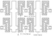
도 3은 본 발명에서 비휘발성 메모리의 레잉아웃(Layout)을 나타낸 도면.3 is a diagram showing the layout of a nonvolatile memory in the present invention.
도 4는 본 발명에 따른 비휘발성 메모리의 셀 어레이를 설명하는 도면.4 illustrates a cell array of a nonvolatile memory in accordance with the present invention.
도 5 내지 도 11은 본 발명에 따른 임베디드 비휘발성 메모리의 제조방법의 제1실시예를 설명하는 도면.5 to 11 illustrate a first embodiment of a method of manufacturing an embedded nonvolatile memory according to the present invention.
도 12과 도 13은 본 발명에서 실리사이드 형성 공정의 다른 실시예를 도시한 도면.12 and 13 illustrate another embodiment of a silicide forming process in the present invention.
본 발명에서는 임베디드 비휘발성 메모리 및 그 제조방법에 관해 개시된다.The present invention relates to an embedded nonvolatile memory and a method of manufacturing the same.
임베디드 비휘발성 메모리(embedded nv(non volatile) Memory)는 비휘발성 메모리 소자와 이를 구동하기 위한 논리회로(logic circuit)를 단일칩에 함께 형성한 것이며, 로직의 기본 기술과 비휘발성 메모리 기술을 접목하여 제조된다.Embedded non-volatile memory (non-volatile memory) is a combination of nonvolatile memory devices and logic circuits for driving them together on a single chip, and combines basic logic and nonvolatile memory technology. Are manufactured.
임베디드 비휘발성 메모리는 여러 가지 타입이 있으며 용도에 따라 적절한 것으로 선택하여 사용하고 있다.There are many types of embedded nonvolatile memory, and they are selected according to their purpose.
임베디드 비휘발성 메모리의 종류로는, 게이트로 작용하는 다결정실리콘층이 단일층인 싱글폴리 이이프롬(single poly EEPROM), 두 개의 다결정실리콘층이 수직으로 적층된 적층게이트(stack gate, ETOX), 싱글폴리 EEPROM과 적층게이트의 중간에 해당하는 듀얼폴리(dual poly) EEPROM과 분리게이트(split gate) 등이 있다.Types of embedded nonvolatile memory include single poly EEPROM, in which a single polysilicon layer acts as a gate, a stack gate (ETOX) in which two polysilicon layers are stacked vertically, and a single layer. There is a dual poly EEPROM and a split gate, which are halfway between a poly EEPROM and a stacked gate.
일반적으로, 적층게이트 타입은 셀 크기가 가장 작은 반면에 회로가 복잡하여 고밀도, 고성능용으로 적합하나, 저밀도용으로는 적합하지 못하다. 저밀도용으로는 EEPROM이 주로 사용된다. 일 예로 싱글폴리 EEPROM은 로직 공정에서 2개정도의 마스크 공정을 추가하면 제작 가능한 반면에, 셀 크기가 적층게이트의 약 200배 가량에 달하므로 고밀도용으로는 적합하지 않는 것이다.In general, the stacked gate type has the smallest cell size, but the circuit is complex, so it is suitable for high density and high performance, but is not suitable for low density. EEPROM is mainly used for low density. For example, a single poly EEPROM can be manufactured by adding about two mask processes in a logic process, while the cell size is about 200 times that of a stacked gate, which is not suitable for high density.
싱글폴리 EEPROM과 적층게이트의 중간에 해당하는 듀얼폴리 EEPROM과 분리게이트 등은 공정이 복잡하다는 단점이 있다.The dual poly EEPROM and the separation gate, which are between the single poly EEPROM and the stacked gate, have a disadvantage in that the process is complicated.
본 발명은 셀 크기가 자고 제조 공정이 간단한 임베디드 비휘발성 메모리 및 그 제조방법을 제공하는 것을 목적으로 한다.An object of the present invention is to provide an embedded nonvolatile memory and a method of manufacturing the same, which have a small cell size and a simple manufacturing process.
본 발명에 따른 임베디드 비휘발성 메모리 제조방법은 반도체 기판에 제1도전형의 불순물 이온 및 제2도전형의 불순물 이온을 주입하여 CMOS 영역 및 EEPROM 영역을 형성하는 단계; 상기 반도체 기판 전면에 게이트 옥사이드를 증착하고, 상기 EEPROM 영역에 폴리 실리콘을 증착하여 패턴 및 에칭공정으로 제1게이트 폴리를 형성하는 단계; 상기 게이트 옥사이드를 제거하고 로직 게이트 옥사이드, 터널 옥사이드 및 커플링 옥사이드를 형성하는 단계; 폴리 실리콘을 증착하고 에칭공정을 통해 상기 CMOS 영역에 로직 게이트 폴리 및 상기 제1게이트 폴리의 측벽에 제2게이트 폴리를 형성하는 단계; 제1도전형의 불순물 이온과 제2도전형의 불순물 이온을 각각 주입하여 소스/드레인 확장 영역을 형성하고 사이드월 스페이서를 형성하는 단계; 및 상기 소스, 드레인, 로직 게이트 폴리에 실리사이드를 형성하는 단계가 포함되어 구성되는 것을 특징으로 한다.In accordance with another aspect of the present invention, there is provided a method of manufacturing an embedded nonvolatile memory, including forming a CMOS region and an EEPROM region by implanting impurity ions of a first conductivity type and impurity ions of a second conductivity type into a semiconductor substrate; Depositing a gate oxide on the entire surface of the semiconductor substrate and depositing polysilicon on the EEPROM region to form a first gate poly by a pattern and an etching process; Removing the gate oxide and forming logic gate oxide, tunnel oxide, and coupling oxide; Depositing poly silicon and forming a logic gate poly in the CMOS region and a second gate poly on sidewalls of the first gate poly through an etching process; Implanting impurity ions of the first conductivity type and impurity ions of the second conductivity type, respectively, to form source / drain extension regions and to form sidewall spacers; And forming silicide on the source, drain, and logic gate poly.
또한, 본 발명에 따른 임베디드 비휘발성 메모리는 반도체 기판에 제1도전형의 불순물 이온 및 제2도전형의 불순물 이온을 주입되어 형성된 CMOS 웰 영역 및 EEPROM 웰 영역; 상기 CMOS 웰 영역 및 EEPROM 웰 영역에 형성된 소스/드레인 영역; 상기 EEPROM 웰 영역에 형성된 게이트 옥사이드 및 제1게이트 폴리; 상기 CMOS 웰 영역에 형성된 로직 게이트 옥사이드와 상기 EEPROM 영역에 형성된 터널 옥사이드 및 커플링 옥사이드; 상기 COMS 영역에 형성된 로직 게이트 폴리; 상기 제1게이트 폴리의 측벽에 형성된 제2게이트 폴리; 및 상기 로직 게이트 폴리 및 상기 제2게이트 폴리의 측벽에 형성된 사이드월 스페이서가 포함되어 구성되는 것을 특징으로 한다.In addition, the embedded nonvolatile memory according to the present invention includes a CMOS well region and an EEPROM well region formed by implanting impurity ions of a first conductivity type and impurity ions of a second conductivity type into a semiconductor substrate; Source / drain regions formed in the CMOS well region and the EEPROM well region; A gate oxide and a first gate poly formed in the EEPROM well region; A logic gate oxide formed in the CMOS well region and a tunnel oxide and a coupling oxide formed in the EEPROM region; A logic gate poly formed in the COMS region; A second gate poly formed on sidewalls of the first gate poly; And sidewall spacers formed on sidewalls of the logic gate poly and the second gate poly.
또한, 본 발명에 따른 임베디드 비휘발성 메모리는 반도체 기판에 형성된 CMOS 트랜지스터 및 EEPROM이 포함되어 구성되는 임베디드 비휘발성 메모리에 있어서, 상기 EEPROM은 상기 반도체 기판에 형성된 제1도전형의 웰과, 상기 제1도전형의 웰에 형성된 소스/드레인 영역과, 상기 제1도전형의 웰 상측에 형성된 게이트 옥사이드 및 제1게이트 폴리와, 상기 소스/드레인 영역 및 제1게이트 폴리에 형성된 터널 옥사이드 및 커플링 옥사이드와, 상기 제1게이트 폴리의 측벽에 형성된 제2게이트 폴리와, 상기 제2게이트 폴리의 측벽에 형성된 사이드월 스페이서가 포함되어 구성되는 것을 특징으로 한다.In addition, the embedded nonvolatile memory according to the present invention includes an embedded nonvolatile memory including a CMOS transistor and an EEPROM formed on a semiconductor substrate, wherein the EEPROM includes a first conductive well formed on the semiconductor substrate, and the first conductive well. Source / drain regions formed in the wells of the conductive type, gate oxides and first gate polys formed on the wells of the first conductivity type, tunnel oxides and coupling oxides formed in the source / drain regions and the first gate polys; And a second gate poly formed on the sidewall of the first gate poly and a sidewall spacer formed on the sidewall of the second gate poly.
이하, 첨부된 도면을 참조하여 본 발명에 따른 임베디드 비휘발성 메모리 및 그 제조방법에 대해 상세히 설명하도록 한다.Hereinafter, an embedded nonvolatile memory and a method of manufacturing the same according to the present invention will be described in detail with reference to the accompanying drawings.
도 1과 도 2는 본 발명에서 비휘발성 메모리의 수직구조를 나타낸 도면이고, 도 3은 본 발명에서 비휘발성 메모리의 레잉아웃(Layout)을 나타낸 도면이다.1 and 2 are views illustrating a vertical structure of a nonvolatile memory in the present invention, and FIG. 3 is a view illustrating a layout of the nonvolatile memory in the present invention.
도 1과 도 2를 참조하면, 제1게이트 폴리(Gate Poly)(10)는 종래의 Floating Gate EEPROM에서의 컨트롤 게이트(Control Gate)와 셀렉트 게이트(Select Gate)의 역할을 동시에 수행하게 된다.Referring to FIGS. 1 and 2, the
다음으로 제2게이트 폴리(11)는 종래의 Floating Gate EEPROM에서의 플로팅 게이트(Floating Gate)와 유사한 작동을 하며 소스 영역(12) 및 드레인 영역(13)을 컨트롤한다.The
도 1은 본 발명의 비휘발성 메모리의 제1실시예이고, 도 2는 본 발명의 비휘발성 메모리의 제2실시예이다.1 is a first embodiment of the nonvolatile memory of the present invention, and FIG. 2 is a second embodiment of the nonvolatile memory of the present invention.
제2실시예에서는 P-웰(well)(14)의 아이솔레이션(Isolation)을 강화하기 위해 P-웰(14)을 딥 N웰(Deep Nwell(15)로 감싸는 트리플 웰(Triple Well) 구조가 형성된다.In the second embodiment, a triple well structure is formed in which the P-
도 3은 본 발명의 비휘발성 메모리의 셀 레이아웃을 설명하는 도면이다.3 is a diagram illustrating a cell layout of a nonvolatile memory of the present invention.
도 3을 참조하면, 본 발명의 비휘발성 메모리의 셀 레이아웃은 종래의 MOS 트랜지스터와 유사한 구조로 되어 있으나, MOS 트랜지스터에서 게이트 폴리(Gate Poly)를 사이드월 스페이서(Sidewall Spacer)가 감싸는 것과 달리 제1게이트 폴리(10)를 제2게이트 폴리(11)가 감싼다.Referring to FIG. 3, the cell layout of the nonvolatile memory of the present invention has a structure similar to that of a conventional MOS transistor, but unlike a sidewall spacer surrounding a gate poly in a MOS transistor, The
또한, 상기 제2게이트 폴리(11) 하측에 LDD 영역을 형성하기 위한 N-type의 불순물 주입이 되어 있지 않다.In addition, an N-type impurity implantation for forming an LDD region is not provided below the
따라서 본 발명의 비휘발성 메모리 제조방법은 종래의 CMOS 소자 제조공정을 대부분 그대로 적용할 수 있으며, 사이드월 스페이서(Sidewall Spacer) 형성공정을 제2게이트 폴리(11) 형성공정으로 변경하여 진행하면 된다.Therefore, in the nonvolatile memory manufacturing method of the present invention, the conventional CMOS device fabrication process may be applied as it is, and the sidewall spacer forming process may be changed to the
즉, 사이드월 스페이서(Sidewall Spacer) 형성 공정 대신 폴리(Poly)를 증착하고, 에치백(Etch Back)공정을 통해 제1게이트 폴리(Gate Poly)(10)의 측벽을 제2게이트 폴리(11)가 감싸도록 하면 된다.That is, instead of forming a sidewall spacer, poly is deposited and an etch back process is used to form sidewalls of the
따라서 본 발명에 따른 비휘발성 메모리는 종래의 Floating Gate EEPROM에 비해 매우 간단한 공정으로 제조할 수 있다. 또한, 일반 MOS 트랜지스터 구조로 되어 있어 단위 셀(Unit Cell) 면적이 종래의 Floating Gate EEPROM 수준으로 매우 작다.Therefore, the nonvolatile memory according to the present invention can be manufactured by a very simple process compared to the conventional floating gate EEPROM. In addition, since the structure of the general MOS transistor, the unit cell (Unit Cell) area is very small compared to the conventional floating gate EEPROM.
따라서 본 발명의 비휘발성 메모리 구조를 사용할 경우 매우 저렴한 비용으로 High Density EEPROM을 구현할 수 있다.Therefore, when the nonvolatile memory structure of the present invention is used, a high density EEPROM can be implemented at a very low cost.
다음으로 본 발명의 비휘발성 메모리의 동작을 위한 바이어스(Bias) 조건은 아래와 같다.Next, a bias condition for the operation of the nonvolatile memory of the present invention is as follows.
[Program 방법][Program Method]
F/N Tunneling 방식 : Vg=+Vp1, Vd=Vs=GND, Vb=Floating or GNDF / N Tunneling Method: Vg = + Vp1, Vd = Vs = GND, Vb = Floating or GND
Hot Electron Injection 방식 : Vg=+Vp2, Vd=+Vd1, Vs=Vb=GNDHot Electron Injection Method: Vg = + Vp2, Vd = + Vd1, Vs = Vb = GND
[Erase 방법][Erase method]
F/N Tunneling 방식1 : Vg=-Ve1, Vd=Vs=GND, Vb=Floating or GNDF / N Tunneling Method 1: Vg = -Ve1, Vd = Vs = GND, Vb = Floating or GND
F/N Tunneling 방식2 : Vg=GND, Vd=Vs=-Ve1, Vb=Floating or GNDF / N Tunneling Method 2: Vg = GND, Vd = Vs = -Ve1, Vb = Floating or GND
[Reading 방법][Reading method]
Vg=+Vref, Vd=+Vd2, Vs=Vb=GNDVg = + Vref, Vd = + Vd2, Vs = Vb = GND
상기와 같이 프로그램 방법은 F/N Tunneling 또는 Hot Electron Injection 방식 중 하나를 사용하여 전자를 제2게이트 폴리(11)에 주입하고, 소거 방법은 F/N Tunneling 방식에 의해 제2게이트 폴리(11)에 주입된 전자를 빼내게 된다.As described above, the program method injects electrons into the
프로그램/소거 상태를 읽어내기 위해 제1게이트 폴리(10)에 기준 전압(Reference Voltage)에 해당하는 +Vref를 인가하고 드레인(Drain)(13)에 적정한Positive Voltage를 인가하게 된다.In order to read the program / erase state, + Vref corresponding to a reference voltage is applied to the
만약, 제2게이트 폴리(11)에 전자가 주입되어 있는 프로그램 상태라고 가정할 경우, 제2게이트 폴리(11) 아래의 소스/드레인 확장영역에 해당하는 부분의 Threshold Voltage가 매우 커지게 된다.If it is assumed that a program state in which electrons are injected into the
따라서, 제1게이트 폴리(10)에 기준 전압(Reference Voltage)을 인가하더라도 제2게이트 폴리(11)의 Threshold Voltage가 기준 전압보다 훨씬 높아 제2게이트 폴리(11) 아래의 소스/드레인 확장영역을 반전시키지 못하게 되어 전류가 흐르지 않게 되어 프로그램 상태를 감지(Sensing)하게 된다.Therefore, even when a reference voltage is applied to the
반대로 제2게이트 폴리(11)에서 전자를 빼낸 소거(Erase)상태라고 가정할 경우 제2게이트 폴리(11) 아래의 소스/드레인 확장영역에 해당하는 부분의 Threshold Voltage가 낮아지게 된다.On the contrary, if the
따라서, 제1게이트 폴리(10)에 Reference Voltage를 인가할 경우 제2게이트 폴리(11)의 Threshold Voltage가 기준전압(Reference Voltage)보다 낮아 제2게이트 폴리(11) 아래의 소스/드레인 확장영역을 반전시키게 되고 이로 인해 드레인(13)에서 소스(12)로 전류가 흐르게 되어 소거(Erase)상태를 감지하게 된다.Therefore, when the reference voltage is applied to the
상기 제2게이트 폴리(11)에 커플링(Coupling)되는 전압은 게이트 폴리(10)와 제2게이트 폴리(11)사이에 형성되는 커패시턴스(Capacitance)와 제2게이트 폴리(11)와 소스/드레인 영역 사이에 만들어지는 커패시턴스의 비, 즉 커플링 비(Coupling Ratio)에 의해 결정되는데, 본 발명의 비휘발성 메모리의 경우 소스/드레인 영역과 제2게이트 폴리(11) 사이에 형성되는 커패시턴스가 제2게이트 폴리(11)와 제1게이트 폴리(10) 사이에 형성되는 커패시턴스보다 훨씬 적어 커플링 비를 0.8이상으로 매우 크게 만들 수 있다.The voltage coupled to the
본 발명의 비휘발성 메모리 제조 공정은 종래의 CMOS 소자 제조공정을 그대로 사용하여 제조되며, 단지 사이드월 스페이서 형성공정을 제2게이트 폴리 형성공정으로 변경하여 진행하면 되기 때문에 종래의 Floating Gate EEPROM에 비해 매우 간단한 공정으로 구현할 수 있다.The nonvolatile memory fabrication process of the present invention is manufactured using the conventional CMOS device fabrication process as it is, and only needs to be changed by changing the sidewall spacer forming process to the second gate poly forming process. It can be implemented in a simple process.
또한, 본 발명의 비휘발성 메모리는 일반 MOS 트랜지스터 구조로 되어 있어 단위 셀 면적이 종래의 Floating Gate EEPROM 수준으로 매우 작게 만들 수 있다.In addition, the nonvolatile memory of the present invention has a general MOS transistor structure, so that the unit cell area can be made very small to the level of the conventional floating gate EEPROM.
또한, 본 발명의 비휘발성 메모리 구조를 사용할 경우 매우 저렴한 비용으로 High Density EEPROM을 구현할 수 있다.In addition, when using the nonvolatile memory structure of the present invention it is possible to implement a high density EEPROM at a very low cost.
또한, 본 발명의 비휘발성 메모리는 High Coupling Ratio를 가지기 때문에 제게이트 폴리에 인가하는 전압의 대부분이 제2게이트 폴리에 그대로 유기되도록 할 수 있어 전압 효율을 높일 수 있다.In addition, since the nonvolatile memory of the present invention has a high coupling ratio, most of the voltage applied to the gate gate poly may be induced in the second gate poly as it is, thereby improving voltage efficiency.
또한, 본 발명의 비휘발성 메모리는 종래의 CMOS 소자 제조 공정을 그대로 사용하기 때문에 로직(Logic) 소자에 임베드(Embed)시키기가 용이하다.In addition, since the nonvolatile memory of the present invention uses a conventional CMOS device fabrication process as it is, it is easy to embed it in a logic device.
이하에서는 임베디드 비휘발성 메모리의 제조방법에 대해 상세히 설명하도록 한다.Hereinafter, a method of manufacturing an embedded nonvolatile memory will be described in detail.
도 4는 본 발명에 따른 비휘발성 메모리의 셀 어레이를 설명하는 도면이다.4 is a diagram illustrating a cell array of a nonvolatile memory according to the present invention.
도 4에 도시된 바와 같이, 본 발명의 비휘발성 메모리는 제1게이트 폴리(10)의 주변을 제2게이트 폴리(11)가 완전히 감싸는 구조로 되어 있다.As shown in FIG. 4, the nonvolatile memory of the present invention has a structure in which the
이와 같이, 제1게이트 폴리(10) 주변을 제2게이트 폴리(11)가 완전히 감싸는 구조로 되어 있어, 커플링 비(Coupling Ratio)를 종래의 Floating Gate 소자 구조에 비해 월등히 크게 만들 수 있다.As such, since the
또한, 제1게이트 폴리(10) 주변을 제2게이트 폴리(11)가 완전히 감싸는 구조로 되어 있어 종래의 Floating Gate 소자와 달리 제2게이트 폴리(11)를 워드 라인(Word line)방향과 비트 라인(Bit Line)방향으로 따로 디파인(Define)할 필요가 없어 매우 간단한 공정으로 제조할 수 있게 된다.In addition, since the
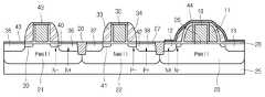
도 5 내지 도 11은 본 발명에 따른 임베디드 비휘발성 메모리의 제조방법의 제1실시예를 설명하는 도면이다.5 to 11 illustrate a first embodiment of a method of manufacturing an embedded nonvolatile memory according to the present invention.
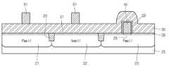
도 5를 참조하면, 패드 옥사이드(24)가 형성된 반도체 기판(25)에 트랜지스터가 형성될 영역들을 STI(20)를 통해 분리시키고 Logic NMOS와, Logic PMOS 및 EEPROM이 형성될 영역에 각각 P웰(21), N웰(22) 및 P웰(23)을 형성시킨다.Referring to FIG. 5, the regions in which the transistors are to be formed in the
도 6을 참조하면, 상기 패드 옥사이드(24)를 제거하고 게이트 옥사이드(26)를 반도체 기판(25)의 전면에서 성장시키고, 폴리 실리콘(Polysilicon)을 반도체 기판(25)의 전면에 증착하고 패턴/에칭 공정을 통해 제1게이트 폴리(10)를 형성한다.Referring to FIG. 6, the
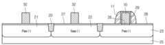
도 7을 참조하면, 상기 게이트 옥사이드(26)을 제거하고 로직 게이트 옥사이드(Logic Gate Oxide)(27)를 성장시킨다.Referring to FIG. 7, the
상기 로직 게이트 옥사이드(27) 성장 공정을 통하여 EEPROM 영역의 터널 옥사이드(Ternnel Oxide)(28)와 커플링 옥사이드(Coupling Oxide)(29)를 동시에 형성시키게 된다.Through the growth process of the
다른 실시예로, 상기 터널 옥사이드(28)와 커플링 옥사이드(29)를 먼저 형성시킨 후, 상기 로직 게이트 옥사이드(27)를 형성할 수 있다.In another embodiment, the
또, 반대로 상기 로직 게이트 옥사이드(27)를 성장시킨 후 상기 터널 옥사이드(28)와 커플링 옥사이드(29)를 성장시킬 수 있다.On the contrary, after the
도 8을 참조하면, 상기 반도체 기판(25)의 전면에 폴리 실리콘(30)을 증착하고 패턴 공정을 통해 로직 게이트 폴리(Logic Gate Poly)가 형성될 영역에만 포토 레지스트(31)를 남긴다. 즉 EEPROM이 형성될 영역에는 포토 레지스트(31)를 모두 제거한다.Referring to FIG. 8,
도 9를 참조하면, 에칭 공정을 통해 로직 게이트 폴리(Logic Gate Poly)(32)를 형성시킨다. 이때 EEPROM 영역 경우 패턴이 형성되어 있지 않기 때문에, 도 9에 도시된 바와 같이 제1게이트 폴리(10)의 둘레에 제2게이트 폴리(11)가 사이드월 스페이서와 같은 형태로 형성된다.Referring to FIG. 9, a
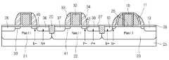
도 10을 참조하면, 불순물 주입을 통해 소스/드레인 확장영역(39,40,41,42)을 형성하고, 사이드월 스페이서(34)를 형성한다. 그리고, 불순물 주입을 통해 소스/드레인 영역(35,36,37,38,12,13)을 형성한다.Referring to FIG. 10, source /
이때 EEPROM 영역의 소스/드레인 영역(12,13)은 N-type 불순물을 주입하여 형성시킨다.In this case, the source /
본 발명에서는 제2게이트 폴리(11) 형성 후 불순물 이온이 주입되기 때문에, 제2게이트 폴리(11)의 하측으로는 직접적으로 불순물이 주입되지 않는다.In the present invention, since the impurity ions are implanted after the
도 11을 참조하면, CMOS 소자의 소스(35,37)/드레인(36,38)/게이트(32)에 실리사이드(Silicide)(43)를 형성시킨다. 이때 EEPROM 영역 경우 실리사이드 블록킹 레이어(Silicide Blocking Layer)(44)를 형성시켜 EEPROM 소자의 소스(12)/드레인(13)/제1게이트 폴리(10)/제2게이트 폴리(11)에 실리사이드가 형성되지 않도록 한다.Referring to FIG. 11,
다른 실시예로, 상기 실리사이드 블록킹 레이어(44)를 제1게이트 폴리(10)와 제2게이트 폴리(11)에만 형성하여, 상기 EEPROM 영역의 소스(11) 및 드레인(13)에 는 실리사이드가 형성되도록 할 수 있다.In another embodiment, the
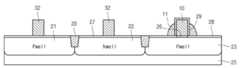
도 12과 도 13은 본 발명에서 실리사이드 형성 공정의 다른 실시예를 도시한 도면이다.12 and 13 illustrate another embodiment of a silicide forming process in the present invention.
도 12와 도 13을 참조하면, 로직 게이트 폴리(32)의 형성을 위한 에칭을 실시할 때 사이드월 형태의 제2게이트 폴리(11)가 제1게이트 폴리(10)의 높이 보다 낮은 높이로 형성될 수 있도록 에칭을 실시한다.12 and 13, when etching to form the
그리고, 사이드월 스페이서(34) 형성시 제2게이트 폴리(11)위에 사이드월 스페이서(34)가 형성되도록 한다.When the
다음으로 EEPROM 영역에 실리사이드 블록킹 레이어를 형성시키지 않음으로써 Logic NMOS/PMOS 소자 뿐만 아니라 EEPROM 소자의 제1게이트 폴리(10)와 소스(12)/드레인(13)에 실리사이드가 형성되도록 한다.Next, by not forming a silicide blocking layer in the EEPROM region, silicide may be formed not only in the Logic NMOS / PMOS device but also in the
한편, 상기 P형 불순물 이온과 N형 불순물 이온은 각각 N형 불순물 이온 및 P형 불순물이온이 주입될 수 있다. 이 경우, EEPROM을 PMOS 소자의 형태로 만들 수 있다.Meanwhile, N-type impurity ions and P-type impurity ions may be implanted into the P-type impurity ions and the N-type impurity ions, respectively. In this case, the EEPROM can be made in the form of a PMOS device.
본 발명의 경우 종래의 CMOS 소자 제조 공정에 포토 패턴(Photo Pattern) 한 공정만 추가하여 임베디드 비휘발성 메모리를 구현할 수 있어 기존 Floating Gate Embedded EEPROM에 비해 공정 구현이 매우 간단하며 제조 비용이 저렴할 뿐만 아니라 공정 개발 기간도 획기적으로 단축시킬 수 있다.In the case of the present invention, it is possible to implement an embedded nonvolatile memory by adding only a photo pattern process to a conventional CMOS device fabrication process, so that the process implementation is very simple and the manufacturing cost is low as well as the process compared to the existing floating gate embedded EEPROM. The development period can also be significantly shortened.
또한, 본 발명은 단위셀 면적을 종래의 Floating Gate EEPROM Cell 수준으로 매우 작게 만들 수 있어 적은 제조 비용으로 High Density EEPROM을 쉽게 구현할 수 있어 기존 Back-bone Standard Logic Process에 1Mb 이하의 MTP(Multi-Time Program)나 OTP(One-Time Program) EEPROM을 임베드 시키는데 적합하다.In addition, the present invention can make the unit cell area very small to the level of the conventional Floating Gate EEPROM Cell, it is possible to easily implement a high density EEPROM with a low manufacturing cost, MTP (Multi-Time less than 1Mb in the existing Back-bone Standard Logic Process) Suitable for embedding a program or one-time program (EPT) EEPROM.
또한, 본 발명의 제1게이트 폴리를 제2게이트 폴리가 완전히 감싸는 구조로 되어 있어 커플링 비(Coupling Ratio)를 매우 높게 만들 수 있어 프로그램(Program) / 소거(Erase) 동작시 인가되는 전압 효율을 높일 수 있다.In addition, the first gate poly of the present invention has a structure in which the second gate poly completely surrounds the coupling ratio, thereby making the coupling ratio very high, thereby improving voltage efficiency applied during program / erase operation. It can increase.
Claims (15)
Translated fromKoreanPriority Applications (2)
| Application Number | Priority Date | Filing Date | Title |
|---|---|---|---|
| KR1020060083859AKR100748003B1 (en) | 2006-08-31 | 2006-08-31 | Embedded nonvolatile memory and its manufacturing method |
| US11/848,670US7625797B2 (en) | 2006-08-31 | 2007-08-31 | Embedded NV memory and method of manufacturing the same |
Applications Claiming Priority (1)
| Application Number | Priority Date | Filing Date | Title |
|---|---|---|---|
| KR1020060083859AKR100748003B1 (en) | 2006-08-31 | 2006-08-31 | Embedded nonvolatile memory and its manufacturing method |
Publications (1)
| Publication Number | Publication Date |
|---|---|
| KR100748003B1true KR100748003B1 (en) | 2007-08-08 |
Family
ID=38602456
Family Applications (1)
| Application Number | Title | Priority Date | Filing Date |
|---|---|---|---|
| KR1020060083859AExpired - Fee RelatedKR100748003B1 (en) | 2006-08-31 | 2006-08-31 | Embedded nonvolatile memory and its manufacturing method |
Country Status (2)
| Country | Link |
|---|---|
| US (1) | US7625797B2 (en) |
| KR (1) | KR100748003B1 (en) |
Cited By (1)
| Publication number | Priority date | Publication date | Assignee | Title |
|---|---|---|---|---|
| KR20160071602A (en)* | 2014-12-12 | 2016-06-22 | 주식회사 윙코 | Dual poly non-volatile memory |
Families Citing this family (5)
| Publication number | Priority date | Publication date | Assignee | Title |
|---|---|---|---|---|
| US8119489B2 (en)* | 2008-03-28 | 2012-02-21 | United Microelectronics Corp. | Method of forming a shallow trench isolation structure having a polysilicon capping layer |
| JP6026914B2 (en)* | 2013-02-12 | 2016-11-16 | ルネサスエレクトロニクス株式会社 | Manufacturing method of semiconductor device |
| KR102227554B1 (en)* | 2014-11-18 | 2021-03-16 | 에스케이하이닉스 주식회사 | Antifuse OTP cell arry and method of opertating the same thereof |
| KR102212751B1 (en) | 2019-07-26 | 2021-02-04 | 주식회사 키 파운드리 | Non-Volatile Memory Device and Manufacturing Method of the same |
| TWI780776B (en)* | 2021-06-16 | 2022-10-11 | 鈺成投資股份有限公司 | How to write the memory multiple times |
Citations (3)
| Publication number | Priority date | Publication date | Assignee | Title |
|---|---|---|---|---|
| KR20050004145A (en)* | 2003-07-04 | 2005-01-12 | 가부시끼가이샤 도시바 | Nonvolatile semiconductor memory and manufacturing method for the same |
| KR20050039085A (en)* | 2003-10-23 | 2005-04-29 | 동부아남반도체 주식회사 | Embedded non volatile memory and fabrication method thereof |
| KR20050082954A (en)* | 2004-02-20 | 2005-08-24 | 삼성전자주식회사 | Non-volitile memory device having oxide charge storage layer |
Family Cites Families (4)
| Publication number | Priority date | Publication date | Assignee | Title |
|---|---|---|---|---|
| US5861347A (en)* | 1997-07-03 | 1999-01-19 | Motorola Inc. | Method for forming a high voltage gate dielectric for use in integrated circuit |
| KR100393205B1 (en)* | 2000-05-30 | 2003-07-31 | 삼성전자주식회사 | Memory merged logic semiconductor device of salicided dual gate structure including embedded memory of self-aligned contact structure and Method of manufacturing the same |
| US6831325B2 (en)* | 2002-12-20 | 2004-12-14 | Atmel Corporation | Multi-level memory cell with lateral floating spacers |
| KR100546691B1 (en)* | 2004-04-23 | 2006-01-26 | 동부아남반도체 주식회사 | Flash memory device, manufacturing method thereof and programming / erasing method |
- 2006
- 2006-08-31KRKR1020060083859Apatent/KR100748003B1/ennot_activeExpired - Fee Related
- 2007
- 2007-08-31USUS11/848,670patent/US7625797B2/ennot_activeExpired - Fee Related
Patent Citations (3)
| Publication number | Priority date | Publication date | Assignee | Title |
|---|---|---|---|---|
| KR20050004145A (en)* | 2003-07-04 | 2005-01-12 | 가부시끼가이샤 도시바 | Nonvolatile semiconductor memory and manufacturing method for the same |
| KR20050039085A (en)* | 2003-10-23 | 2005-04-29 | 동부아남반도체 주식회사 | Embedded non volatile memory and fabrication method thereof |
| KR20050082954A (en)* | 2004-02-20 | 2005-08-24 | 삼성전자주식회사 | Non-volitile memory device having oxide charge storage layer |
Cited By (2)
| Publication number | Priority date | Publication date | Assignee | Title |
|---|---|---|---|---|
| KR20160071602A (en)* | 2014-12-12 | 2016-06-22 | 주식회사 윙코 | Dual poly non-volatile memory |
| KR101668839B1 (en)* | 2014-12-12 | 2016-10-24 | 주식회사 윙코 | Dual poly non-volatile memory |
Also Published As
| Publication number | Publication date |
|---|---|
| US20080054335A1 (en) | 2008-03-06 |
| US7625797B2 (en) | 2009-12-01 |
Similar Documents
| Publication | Publication Date | Title |
|---|---|---|
| US8344443B2 (en) | Single poly NVM devices and arrays | |
| US7859043B2 (en) | Three-terminal single poly NMOS non-volatile memory cell | |
| JP6092315B2 (en) | Highly scalable single poly nonvolatile memory cell | |
| TWI502688B (en) | Non-volatile memory bit cell with a replacement control gate and an additional floating gate | |
| US7919368B2 (en) | Area-efficient electrically erasable programmable memory cell | |
| TWI649858B (en) | Non-volatile memory and manufacturing method thereof | |
| US20180277478A1 (en) | Semiconductor device | |
| EP2639816B1 (en) | Method of fabricating a single-poly floating-gate memory device | |
| KR100932134B1 (en) | Single polypyropyrom and preparation method thereof | |
| CN107527917B (en) | 1.5T depletion type SONOS non-volatile memory and manufacturing method thereof | |
| KR100748003B1 (en) | Embedded nonvolatile memory and its manufacturing method | |
| US8722496B1 (en) | Method for making embedded cost-efficient SONOS non-volatile memory | |
| US8344440B2 (en) | Three-terminal single poly NMOS non-volatile memory cell with shorter program/erase times | |
| US8334559B2 (en) | Semiconductor storage device and manufacturing method | |
| CN101005075A (en) | Non-volatile memory and its manufacturing method | |
| CN110739313B (en) | A kind of non-volatile memory cell, array and preparation method | |
| JP5196670B2 (en) | Method for erasing an EEPROM device | |
| TWI521683B (en) | Erasable programmable single-poly nonvolatile memory | |
| US8906762B2 (en) | Flash memory with P-type floating gate | |
| JP7245171B2 (en) | Semiconductor device and method of operation thereof | |
| KR100953348B1 (en) | Monopolyypyrom and process for preparing same | |
| JP3940477B2 (en) | Semiconductor device | |
| JP5236910B2 (en) | Nonvolatile semiconductor memory device | |
| US7888272B2 (en) | Methods for manufacturing memory and logic devices using the same process without the need for additional masks | |
| CN119446231A (en) | Multi-time programmable memory cell and storage device |
Legal Events
| Date | Code | Title | Description |
|---|---|---|---|
| A201 | Request for examination | ||
| PA0109 | Patent application | St.27 status event code:A-0-1-A10-A12-nap-PA0109 | |
| PA0201 | Request for examination | St.27 status event code:A-1-2-D10-D11-exm-PA0201 | |
| E701 | Decision to grant or registration of patent right | ||
| PE0701 | Decision of registration | St.27 status event code:A-1-2-D10-D22-exm-PE0701 | |
| GRNT | Written decision to grant | ||
| PR0701 | Registration of establishment | St.27 status event code:A-2-4-F10-F11-exm-PR0701 | |
| PR1002 | Payment of registration fee | St.27 status event code:A-2-2-U10-U11-oth-PR1002 Fee payment year number:1 | |
| PG1601 | Publication of registration | St.27 status event code:A-4-4-Q10-Q13-nap-PG1601 | |
| PR1001 | Payment of annual fee | St.27 status event code:A-4-4-U10-U11-oth-PR1001 Fee payment year number:4 | |
| FPAY | Annual fee payment | Payment date:20110719 Year of fee payment:5 | |
| PR1001 | Payment of annual fee | St.27 status event code:A-4-4-U10-U11-oth-PR1001 Fee payment year number:5 | |
| FPAY | Annual fee payment | Payment date:20120726 Year of fee payment:6 | |
| PR1001 | Payment of annual fee | St.27 status event code:A-4-4-U10-U11-oth-PR1001 Fee payment year number:6 | |
| PN2301 | Change of applicant | St.27 status event code:A-5-5-R10-R11-asn-PN2301 | |
| PN2301 | Change of applicant | St.27 status event code:A-5-5-R10-R14-asn-PN2301 | |
| L13-X000 | Limitation or reissue of ip right requested | St.27 status event code:A-2-3-L10-L13-lim-X000 | |
| U15-X000 | Partial renewal or maintenance fee paid modifying the ip right scope | St.27 status event code:A-4-4-U10-U15-oth-X000 | |
| LAPS | Lapse due to unpaid annual fee | ||
| PC1903 | Unpaid annual fee | St.27 status event code:A-4-4-U10-U13-oth-PC1903 Not in force date:20130803 Payment event data comment text:Termination Category : DEFAULT_OF_REGISTRATION_FEE | |
| PC1903 | Unpaid annual fee | St.27 status event code:N-4-6-H10-H13-oth-PC1903 Ip right cessation event data comment text:Termination Category : DEFAULT_OF_REGISTRATION_FEE Not in force date:20130803 | |
| P22-X000 | Classification modified | St.27 status event code:A-4-4-P10-P22-nap-X000 | |
| P22-X000 | Classification modified | St.27 status event code:A-4-4-P10-P22-nap-X000 | |
| P22-X000 | Classification modified | St.27 status event code:A-4-4-P10-P22-nap-X000 |