KR100747485B1 - A semiconductor device and a method of manufacturing the same - Google Patents
A semiconductor device and a method of manufacturing the sameDownload PDFInfo
- Publication number
- KR100747485B1 KR100747485B1KR1020057015937AKR20057015937AKR100747485B1KR 100747485 B1KR100747485 B1KR 100747485B1KR 1020057015937 AKR1020057015937 AKR 1020057015937AKR 20057015937 AKR20057015937 AKR 20057015937AKR 100747485 B1KR100747485 B1KR 100747485B1
- Authority
- KR
- South Korea
- Prior art keywords
- substrate
- flash memory
- chip
- memory card
- electrodes
- Prior art date
- Legal status (The legal status is an assumption and is not a legal conclusion. Google has not performed a legal analysis and makes no representation as to the accuracy of the status listed.)
- Expired - Fee Related
Links
Images


Classifications
- G—PHYSICS
- G06—COMPUTING OR CALCULATING; COUNTING
- G06K—GRAPHICAL DATA READING; PRESENTATION OF DATA; RECORD CARRIERS; HANDLING RECORD CARRIERS
- G06K19/00—Record carriers for use with machines and with at least a part designed to carry digital markings
- G06K19/06—Record carriers for use with machines and with at least a part designed to carry digital markings characterised by the kind of the digital marking, e.g. shape, nature, code
- G06K19/067—Record carriers with conductive marks, printed circuits or semiconductor circuit elements, e.g. credit or identity cards also with resonating or responding marks without active components
- G06K19/07—Record carriers with conductive marks, printed circuits or semiconductor circuit elements, e.g. credit or identity cards also with resonating or responding marks without active components with integrated circuit chips
Landscapes
- Engineering & Computer Science (AREA)
- Computer Hardware Design (AREA)
- Microelectronics & Electronic Packaging (AREA)
- Physics & Mathematics (AREA)
- General Physics & Mathematics (AREA)
- Theoretical Computer Science (AREA)
- Credit Cards Or The Like (AREA)
- Instrument Panels (AREA)
- Details Or Accessories Of Spraying Plant Or Apparatus (AREA)
- Application Of Or Painting With Fluid Materials (AREA)
Abstract
Translated fromKoreanDescription
Translated fromKorean도 1은 본 발명의 일 실시예인 반도체 장치 및 보조 기구의 사시도.1 is a perspective view of a semiconductor device and an auxiliary mechanism according to one embodiment of the present invention.
도 2의 (a)는 도 1의 반도체 장치의 표면측의 외관을 도시한 사시도.FIG. 2A is a perspective view showing the appearance of the surface side of the semiconductor device of FIG. 1; FIG.
도 2의 (b)는 그 반도체 장치의 이면측의 외관을 도시한 사시도.Fig. 2B is a perspective view showing the appearance of the back side of the semiconductor device.
도 3의 (a)는 도 1의 반도체 장치의 표면측의 평면도.3A is a plan view of the surface side of the semiconductor device of FIG.
도 3의 (b)는 도 3의 (a)의 반도체 장치의 측면도.(B) is a side view of the semiconductor device of (a) of FIG.
도 3의 (c)는 도 3의 (a)의 반도체 장치의 배면도.FIG. 3C is a rear view of the semiconductor device of FIG. 3A.
도 3의 (d)는 도 3의 (a)의 반도체 장치의 이면측의 평면도.(D) is a top view of the back surface side of the semiconductor device of FIG.
도 4의 (a)는 도 1의 반도체 장치의 길이 방향에서의 보조 기구 장착부의 주요부 확대 단면도.FIG. 4A is an enlarged cross-sectional view of an essential part of an auxiliary mechanism mounting unit in the longitudinal direction of the semiconductor device of FIG. 1.
도 4의 (b)는 도 1의 반도체 장치의 짧은 방향에서의 보조 기구 장착부의 주요부 확대 단면도.FIG. 4B is an enlarged cross-sectional view of an essential part of an auxiliary mechanism mounting portion in a short direction of the semiconductor device of FIG. 1.
도 5의 (a)는 도 3의 (a)의 A-A선의 단면도.(A) is sectional drawing of the A-A line | wire of (a) of FIG.
도 5의 (b)는 도 5의 (a)의 주요부 확대 단면도.FIG. 5B is an enlarged cross-sectional view of a main part of FIG. 5A. FIG.
도 6은 도 1의 반도체 장치의 베이스 기판의 평면도.6 is a plan view of a base substrate of the semiconductor device of FIG.
도 7의 (a)는 도 1의 보조 기초부의 표면측의 평면도.Fig. 7A is a plan view of the surface side of the auxiliary base of Fig. 1.
도 7의 (b)는 도 7의 (a)의 보조 기구의 측면도.Fig. 7B is a side view of the auxiliary mechanism of Fig. 7A.
도 7의 (c)는 도 7의 (a)의 보조 기구의 배면도.(C) is a rear view of the auxiliary mechanism of (a) of FIG.
도 7의 (d)는 도 7의 (a)의 보조 기구의 이면측의 평면도.Fig. 7D is a plan view of the back side of the auxiliary mechanism of Fig. 7A.
도 7의 (e)는 도 7의 (a)의 보조 기구의 갈고리부 및 지지부의 주요부 확대 단면도.Fig. 7E is an enlarged sectional view of the main part of the hook portion and the support portion of the auxiliary mechanism of Fig. 7A.
도 8의 (a)는 도 1의 반도체 장치 및 보조 기구의 표면의 평면도.8A is a plan view of the surface of the semiconductor device and auxiliary mechanism of FIG. 1;
도 8의 (b)는 도 8의 (a)의 측면도.(B) is a side view of FIG. 8 (a).
도 8의 (c)는 도 8의 (a)의 이면의 평면도.(C) is a top view of the back surface of (a) of FIG.
도 9의 (a)는 기존의 풀 사이즈의 반도체 장치의 표면의 평면도.9A is a plan view of the surface of a conventional full-size semiconductor device.
도 9의 (b)는 도 9의 (a)의 측면도.FIG. 9B is a side view of FIG. 9A.
도 9의 (c)는 도 9의 (a)의 이면의 평면도.(C) is a top view of the back surface of (a) of FIG.
도 10의 (a)는 도 8의 상태의 반도체 장치의 보조 기구 갈고리 장착부와, 보조 기구의 갈고리부와의 접합부의 주요부 확대 단면도.Fig. 10A is an enlarged cross sectional view of the main portion of the junction portion between the auxiliary mechanism hook attachment portion and the hook portion of the auxiliary mechanism in the semiconductor device shown in Fig. 8;
도 10의 (b)는 도 8의 상태의 반도체 장치의 보조 기구 장착부와, 보조 기구의 오목부와의 접합부의 주요부 확대 단면도.FIG. 10B is an enlarged cross-sectional view of an essential part of a junction between the auxiliary device mounting portion of the semiconductor device in the state of FIG.
도 11은 도 1의 반도체 장치의 일부재를 성형하기 위한 금형의 단면도.11 is a cross-sectional view of a mold for molding a part of the semiconductor device of FIG. 1.
도 12(a)∼(c)는 도 11의 주요부 확대 단면도.12 (a) to 12 (c) are enlarged cross-sectional views of main parts of FIG.
도 13의 (a)는 반도체 장치의 전체 평면도.13A is an overall plan view of a semiconductor device.
도 13의 (b)는 도 13의 (a)의 반도체 장치의 기판을 풀 사이즈의 반도체 장치에 내장하여 사용한 경우의 전체 평면도.FIG. 13B is an overall plan view of the case where the substrate of the semiconductor device of FIG. 13A is incorporated into a full-size semiconductor device and used. FIG.
도 14는 본 발명의 다른 실시예인 반도체 장치 및 보조 기구의 사시도.14 is a perspective view of a semiconductor device and an auxiliary mechanism according to another embodiment of the present invention.
도 15의 (a), (b)는 도 14의 반도체 장치의 표면측 및 이면측의 외관을 도시한 사시도.15A and 15B are perspective views showing the appearance of the front and back sides of the semiconductor device of FIG.
도 16의 (a)는 도 14의 반도체 장치의 표면측의 평면도.FIG. 16A is a plan view of the surface side of the semiconductor device of FIG.
도 16의 (b)는 도 16의 (a)의 반도체 장치의 측면도.FIG. 16B is a side view of the semiconductor device of FIG. 16A.
도 16의 (c)는 도 16의 (a)의 반도체 장치의 배면도.FIG. 16C is a rear view of the semiconductor device of FIG. 16A.
도 16의 (d)는 도 16의 (a)의 반도체 장치의 이면측의 평면도.(D) is a top view of the back surface side of the semiconductor device of FIG.
도 17의 (a)는 도 14의 반도체 장치 및 보조 기구의 표면의 평면도.17A is a plan view of the surface of the semiconductor device and auxiliary mechanism of FIG. 14;
도 17의 (b)는 도 17의 (a)의 측면도.FIG. 17B is a side view of FIG. 17A.
도 17의 (c)는 도 17의 (a)의 이면의 평면도.(C) is a top view of the back surface of (a) of FIG.
도 18은 본 발명의 또 다른 실시예인 반도체 장치의 이면측의 평면도.18 is a plan view of the back side of a semiconductor device according to another embodiment of the present invention.
도 19는 본 발명자가 검토한 반도체 장치의 베이스 기판의 표면의 평면도.Fig. 19 is a plan view of the surface of the base substrate of the semiconductor device examined by the inventor.
도 20은 도 19의 베이스 기판의 이면의 평면도.20 is a plan view of the rear surface of the base substrate of FIG. 19;
도 21은 본 발명자가 검토한 풀 사이즈의 반도체 장치용의 캡의 표면의 평면도.Fig. 21 is a plan view of the surface of a cap for a full-size semiconductor device examined by the inventor.
도 22는 도 21의 캡에서의 이면의 평면도.FIG. 22 is a plan view of the back side of the cap of FIG. 21; FIG.
도 23은 도 19 및 도 20에 도시한 베이스 기판을, 도 21 및 도 22의 캡의 홈에 설치한 후의 풀 사이즈의 반도체 장치의 이면의 평면도.FIG. 23 is a plan view of the rear surface of a full-size semiconductor device after the base substrate shown in FIGS. 19 and 20 is provided in the groove of the cap of FIGS. 21 and 22.
도 24는 본 발명의 일 실시예에서의 반도체 장치를 구성하는 베이스 기판의 표면의 평면도.24 is a plan view of the surface of a base substrate constituting a semiconductor device in one embodiment of the present invention;
도 25는 도 24의 베이스 기판에서의 이면의 평면도.25 is a plan view of the rear face of the base substrate of FIG. 24;
도 26은 도 24 및 도 25에 도시한 베이스 기판을 탑재하는 풀 사이즈의 반도체 장치용의 캠프에서의 표면의 평면도.FIG. 26 is a plan view of a surface of a camp for a full-size semiconductor device on which the base substrates shown in FIGS. 24 and 25 are mounted;
도 27은 도 26의 캡에서의 이면의 평면도.FIG. 27 is a plan view of the rear face of the cap of FIG. 26; FIG.
도 28은 도 24 및 도 25에 도시한 베이스 기판을, 도 26 및 도 27의 캡에 설치한 후의 풀 사이즈의 반도체 장치에서의 이면의 평면도.FIG. 28 is a plan view of the rear surface of a full-size semiconductor device after the base substrate shown in FIGS. 24 and 25 is provided in the cap of FIGS. 26 and 27.
도 29는 도 28의 A1-A1선의 단면도.29 is a cross-sectional view taken along a line A1-A1 in FIG. 28;
도 30은 도 23에 도시한 반도체 장치의 구부러짐 강도 시험의 결과의 설명도.30 is an explanatory diagram of results of bending strength tests of the semiconductor device illustrated in FIG. 23.
도 31은 도 23에 도시한 반도체 장치의 구부러짐 강도 시험의 결과의 설명도.FIG. 31 is an explanatory diagram of results of a bending strength test of the semiconductor device shown in FIG. 23; FIG.
도 32는 도 23에 도시한 반도체 장치의 구부러짐 강도 시험의 결과의 설명도.FIG. 32 is an explanatory diagram of results of a bending strength test of the semiconductor device shown in FIG. 23; FIG.
도 33은 본 발명의 일 실시예인 반도체 장치의 구부러짐 강도 시험의 결과의 설명도.33 is an explanatory diagram of results of a bending strength test of a semiconductor device of one embodiment of the present invention;
도 34는 본 발명의 일 실시예인 반도체 장치의 구부러짐 강도 시험의 결과의 설명도.34 is an explanatory diagram of results of a bending strength test of a semiconductor device of one embodiment of the present invention;
도 35는 본 발명의 일 실시예인 반도체 장치의 구부러짐 강도 시험의 결과의 설명도.35 is an explanatory diagram of results of a bending strength test of a semiconductor device of one embodiment of the present invention;
도 36은 본 발명의 일 실시예인 반도체 장치의 캡에서의 이면의 평면도.36 is a plan view of the back surface of the cap of the semiconductor device of one embodiment of the present invention.
도 37은 본 발명의 일 실시예인 반도체 장치의 주요부 확대 단면도.37 is an enlarged cross-sectional view of an essential part of a semiconductor device of one embodiment of the present invention;
도 38은, 도 26∼도 29 등에 도시한 반도체 장치의 캡을 성형하는 금형의 일례의 단면도.38 is a cross-sectional view of an example of a mold for molding a cap of the semiconductor device shown in FIGS. 26 to 29 and the like.
도 39는 본 발명의 일 실시예인 반도체 장치의 칩의 배치예를 도시한 베이스 기판의 표면의 평면도.39 is a plan view of the surface of a base substrate, showing an arrangement example of chips in a semiconductor device according to one embodiment of the present invention;
도 40은 본 발명의 일 실시예인 반도체 장치의 칩의 배치예를 도시한 베이스 기판의 표면의 평면도.40 is a plan view of the surface of a base substrate, showing an arrangement example of chips in a semiconductor device of one embodiment of the present invention;
도 41은 본 발명의 일 실시예인 반도체 장치의 조립 공정의 흐름도.41 is a flowchart of an assembly process of a semiconductor device of one embodiment of the present invention.
도 42는 도 41의 반도체 장치의 조립 공정 중에서의 베이스 기판의 표면의 평면도.42 is a plan view of the surface of the base substrate during the assembly process of the semiconductor device of FIG. 41;
도 43은 도 42에 계속되는 반도체 장치의 조립 공정 중에서의 베이스 기판의 표면의 평면도.43 is a plan view of the surface of the base substrate during the assembly process of the semiconductor device subsequent to FIG. 42;
도 44는 도 43에 계속되는 반도체 장치의 조립 공정 중에서의 베이스 기판의 표면의 평면도.44 is a plan view of the surface of the base substrate during the assembly process of the semiconductor device subsequent to FIG. 43;
도 45는 도 44에 계속되는 반도체 장치의 조립 공정 중에서의 베이스 기판의 표면의 평면도.45 is a plan view of the surface of the base substrate during the assembly process of the semiconductor device subsequent to FIG. 44;
도 46은 도 45에 계속되는 반도체 장치의 조립 공정 중에서의 베이스 기판의 표면의 평면도.46 is a plan view of the surface of the base substrate during the assembly process of the semiconductor device subsequent to FIG. 45;
도 47은 본 발명의 다른 실시예인 풀 사이즈의 반도체 장치에서의 이면의 평면도.47 is a plan view of the back side of a full size semiconductor device of another embodiment of the present invention.
도 48은 도 47의 영역 Z1의 확대 평면도.48 is an enlarged plan view of the region Z1 of FIG. 47.
도 49는 본 발명의 다른 실시예인 풀 사이즈의 반도체 장치에서의 이면의 평면도.49 is a plan view of the back side of a full size semiconductor device of another embodiment of the present invention.
도 50은 도 49의 영역 Z2의 확대 평면도.50 is an enlarged plan view of the region Z2 in FIG. 49.
도 51은 본 발명의 다른 실시예인 풀 사이즈의 반도체 장치에서의 이면의 평면도.51 is a plan view of the rear face of a full size semiconductor device of another embodiment of the present invention.
도 52는 본 발명의 다른 실시예인 하프 사이즈의 반도체 장치의 표면에서의 평면도.52 is a plan view of the surface of a half-size semiconductor device according to another embodiment of the present invention.
도 53은 도 52의 반도체 장치의 이면에서의 평면도.53 is a plan view from the back of the semiconductor device of FIG. 52;
도 54는 본 발명의 다른 실시예인 하프 사이즈의 반도체 장치의 이면에서의 평면도.54 is a plan view of the back surface of a half-size semiconductor device of another embodiment of the present invention.
도 55는 본 발명의 또 다른 실시예인 하프 사이즈의 반도체 장치의 이면에서의 평면도.Fig. 55 is a plan view of the back side of a half-size semiconductor device according to still another embodiment of the present invention.
도 56은 본 발명의 다른 실시예인 풀 사이즈의 반도체 장치의 단면도.56 is a sectional view of a full size semiconductor device of another embodiment of the present invention.
도 57은 도 56의 주요부 확대 단면도.FIG. 57 is an enlarged sectional view of an essential part of FIG. 56; FIG.
<도면의 주요 부분에 대한 부호의 설명><Explanation of symbols for the main parts of the drawings>
1: 메모리 카드1: memory card
2: 어댑터(보조 기구)2: adapter (auxiliary device)
3: 캡(케이스 본체)3: cap (case body)
4: 베이스 기판4: base substrate
5: 반도체 칩5: semiconductor chip
6: 본딩 와이어6: bonding wire
7, 9: 접속 단자7, 9: connection terminal
8: 테스트 패드8: test pad
10: 관통 홀10: through hole
11: 밀봉 수지11: sealing resin
본 발명은, 반도체 장치 및 그 제조 기술에 관한 것으로, 예를 들면 반도체 메모리 카드(이하, 단순히 메모리 카드)에 적용하기에 유효한 기술에 관한 것이다.BACKGROUND OF THE
멀티미디어 카드(미국 선 디스크사)나 SD 카드(파나소닉, 도시바, 선 디스크) 등과 같은 메모리 카드는, 그 내부의 반도체 메모리 칩에 정보를 기억하는 기억 장치의 하나이다. 이 메모리 카드에서는, 반도체 메모리 칩에 형성된 불휘발성 메모리에 대하여 정보를 직접적이고, 또한 전기적으로 액세스하는 것이기 때문에, 기계계의 제어가 없는 만큼, 다른 기억 장치에 비해 기입, 판독의 시간이 빠른 데다가, 기억 매체의 교환이 가능하다. 또한, 형상이 비교적 소형으로 가볍기 때문에, 주로 휴대형 퍼스널 컴퓨터, 휴대 전화 또는 디지털 카메라 등과 같은 운반 가능성이 요구되는 기기의 보조 기억 장치로서 사용되고 있다. 최근에는, 이 기기의 소형화가 진행되고 있으며, 그에 따라 메모리 카드의 한층 더 소형화가 요구되고 있다. 또한, 메모리 카드는 새로운 기술이기도 하고, 그 치수 상의 규격이 완전하게 통일되어 있지 않다.A memory card such as a multimedia card (US sun disk company) or an SD card (Panasonic, Toshiba, sun disk) or the like is one of memory devices for storing information in a semiconductor memory chip therein. In this memory card, since the information is directly and electrically accessed to the nonvolatile memory formed in the semiconductor memory chip, the time required for writing and reading is faster than that of other storage devices because there is no control of the mechanical system. Exchange of storage media is possible. In addition, since the shape is relatively small and light, it is mainly used as an auxiliary storage device for equipment that requires portability, such as a portable personal computer, a mobile phone or a digital camera. In recent years, miniaturization of this apparatus is progressing, and accordingly, further miniaturization of a memory card is calculated | required. In addition, the memory card is also a new technology, and its size standard is not completely unified.
그런데, 메모리 카드의 사이즈를 작게 하는 경우나 혹은 나라에 따라 사이즈가 다른 경우에는, 어떤 방법으로든, 기존의 메모리 카드와의 치수 상의 호환성을 유지하여, 기존의 메모리 카드 대응 기기에 대하여 사용할 수 있도록 하는 것이 중요한 과제가 된다.By the way, when the size of the memory card is reduced or the size is different depending on the country, it is possible to maintain the compatibility with the existing memory card in any way so that it can be used with existing memory card compatible devices. It is an important task.
본 발명의 목적은, 반도체 장치의 범용성을 높일 수 있는 기술을 제공하는 것에 있다.An object of the present invention is to provide a technique capable of increasing the versatility of a semiconductor device.
본 발명의 상기 및 그 밖의 목적과 새로운 특징은, 본 명세서의 기술 및 첨부 도면으로부터 분명해질 것이다.The above and other objects and novel features of the present invention will become apparent from the description and the accompanying drawings.
<발명의 개시><Start of invention>
본원에서 개시되는 발명 중, 대표적인 것의 개요를 간단히 설명하면 다음과 같다.Among the inventions disclosed herein, an outline of representative ones will be briefly described as follows.
즉, 본 발명은 반도체 칩을 내장하는 수지제의 케이스 본체의 평면 치수를 변환하기 위한 금속제의 보조 기구의 오목부를 끼움으로써, 상기 케이스 본체에 상기 보조 기구를 착탈 가능한 상태로 장착 가능한 단면 볼록형 장착부를 상기 케이스 본체에 설치한 것이다.That is, the present invention provides a cross-sectional convex mounting portion capable of attaching the auxiliary mechanism to the case body in a detachable state by inserting a recess of a metal auxiliary mechanism for converting the plane dimensions of the case body made of a resin containing a semiconductor chip. It is installed in the case body.
또한, 본 발명은 반도체 칩이 탑재된 기판의 부품 탑재면을 덮도록 피복한 수지제의 케이스 본체의 평면적의 절반 또는 그 이하의 면적의 기판을 갖는 것이 다.Moreover, this invention has a board | substrate of half or less of the plane area of the resin case main body which coat | covered the component mounting surface of the board | substrate with which the semiconductor chip was mounted.
또한, 본 발명은 하측 금형의 캐비티 깊이가 상측 금형의 캐비티 깊이보다도 큰 몰드 금형을 이용하여, 반도체 칩이 탑재된 기판의 부품 탑재면을 피복하기 위한 케이스 본체를 성형하는 공정을 포함하는 것이다.Moreover, this invention includes the process of shape | molding the case main body for covering the component mounting surface of the board | substrate with which the semiconductor chip was mounted using the mold mold whose cavity depth of a lower metal mold | die is larger than the cavity depth of an upper metal mold | die.
또한, 본 발명은 케이스 본체와, 상기 케이스 본체의 일면에 형성된 홈과, 상기 홈 내에 부품 탑재면을 향한 상태로 설치된 기판과, 상기 부품 탑재면에 탑재된 복수의 반도체 칩을 구비하고, 상기 홈 및 상기 기판에 있어서 상기 케이스 본체의 길이 방향을 따르는 길이는, 상기 케이스 본체의 길이 방향의 전체 길이보다도 짧아지도록 형성되어 있고, 상기 기판 및 상기 홈에 있어서 케이스 본체 중앙측에 위치하는 각부를 모따기한 것이다.In addition, the present invention includes a case main body, a groove formed on one surface of the case main body, a substrate provided in a state facing the component mounting surface in the groove, and a plurality of semiconductor chips mounted on the component mounting surface. And the length along the longitudinal direction of the case main body in the substrate is shorter than the total length in the longitudinal direction of the case main body, and the chamfered portions located at the center of the case main body in the substrate and the groove. will be.
이하의 실시예에서는 편의상 그 필요가 있을 때는, 복수의 섹션 또는 실시예로 분할하여 설명하지만, 특별히 명시한 경우를 제외하고, 이들은 상호 무관한 것이 아니며, 한쪽은 다른 쪽의 일부 또는 모든 변형예, 상세, 보충 설명 등의 관계에 있다.In the following embodiments, when necessary for the sake of convenience, the description is divided into a plurality of sections or embodiments, but unless otherwise specified, they are not related to each other, and one side is a part or all of the other modifications and details. , Supplementary explanations, etc.
또한, 이하의 실시예에서, 요소의 수 등(개수, 수치, 양, 범위 등을 포함)을 언급하는 경우, 특별히 명시한 경우 및 원리적으로 분명히 특정한 수에 한정되는 경우 등을 제외하고, 그 특정한 수에 한정되는 것이 아니며, 특정한 수 이상이든, 이하이든 무방하다.In addition, in the following examples, when referring to the number of elements and the like (including number, numerical value, amount, range, etc.), except for the case where it is specifically stated, and the principle is clearly limited to a specific number, etc. It is not limited to the number, It may be more than the specific number, or less.
또한, 이하의 실시예에서, 그 구성 요소(요소 스텝 등도 포함)는, 특별히 명 시한 경우 및 원리적으로 분명히 필수라고 생각되는 경우 등을 제외하고, 반드시 필수적인 것이 아닌 것은 물론이다.Incidentally, in the following embodiments, the components (including the element steps and the like) are not necessarily essential, except in the case where it is specifically stated and when it is deemed necessary in principle.
마찬가지로, 이하의 실시예에서 구성 요소 등의 형상, 위치 관계 등을 언급할 때는, 특별히 명시한 경우 및 원리적으로 분명히 그렇지 않다고 생각되는 경우 등을 제외하고, 실질적으로 그 형상 등에 근사하거나 또는 유사한 것 등을 포함하는 것으로 한다. 이것은, 상기 수치 및 범위에 대해서도 마찬가지다.Similarly, when referring to the shape, positional relationship, etc. of the component or the like in the following embodiments, substantially similar to or similar to the shape or the like, except in the case where it is specifically stated and when it is deemed obviously not in principle. It shall be included. This also applies to the above numerical values and ranges.
또한, 본 실시예를 설명하기 위한 전체 도면에서 동일 기능을 갖는 것은 동일한 부호를 붙여, 그 반복의 설명은 생략한다.In addition, in the whole figure for demonstrating this embodiment, the thing with the same function attaches | subjects the same code | symbol, and description of the repetition is abbreviate | omitted.
또한, 본 실시예에서 이용하는 도면에서는, 평면도에서도 도면을 보기 쉽게 하기 위해 해칭으로 표시하는 경우도 있다.In addition, in the drawing used by a present Example, even in plan view, in order to make drawing easy to see, it may display by hatching.
이하, 본 발명의 실시예를 도면에 기초하여 상세히 설명한다.Hereinafter, embodiments of the present invention will be described in detail with reference to the drawings.
(실시예 1)(Example 1)
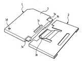
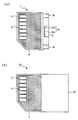
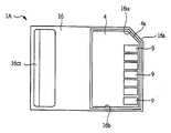
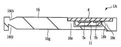
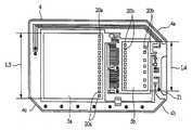
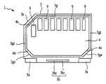
도 1은, 본 발명의 일 실시예인 반도체 장치 및 보조 기구의 사시도, 도 2 (a), (b)는, 도 1의 반도체 장치의 표면측 및 이면측의 외관을 도시한 사시도, 도 3의 (a)는 도 1의 반도체 장치의 표면측의 평면도, 도 3의 (b)는 (a)의 반도체 장치의 측면도, 도 3의 (c)는 (a)의 반도체 장치의 배면도, 도 3의 (d)는 (a)의 반도체 장치의 이면측의 평면도, 도 4의 (a)는 도 1의 반도체 장치의 길이 방향에서의 보조 기구 장착부의 주요부 확대 단면도, 도 4의 (b)는 도 1의 반도체 장치의 짧은 방향에서의 보조 기구 장착부의 주요부 확대 단면도, 도 5의 (a)는 도 3의 (a)의 반도체 장치의 짧은 방향(A-A 선)의 단면도, 도 5의 (b)는 도 5의 (a)의 주요부 확 대 단면도, 도 6은 이 반도체 장치의 베이스 기판의 평면도를 도시하고 있다.1 is a perspective view of a semiconductor device and an auxiliary mechanism according to an embodiment of the present invention, and FIGS. 2A and 2B are perspective views showing the appearance of the front and back sides of the semiconductor device of FIG. (a) is a top view of the surface side of the semiconductor device of FIG. 1, FIG. 3 (b) is a side view of the semiconductor device of (a), FIG. 3 (c) is a rear view of the semiconductor device of (a), and FIG. (D) is a top view of the back side of the semiconductor device of (a), FIG. 4 (a) is an enlarged sectional view of the main part of the auxiliary mechanism mounting portion in the longitudinal direction of the semiconductor device of FIG. 1, and (b) of FIG. An enlarged cross-sectional view of an essential part of the auxiliary mechanism mounting portion in the short direction of the semiconductor device of FIG. 1, FIG. 5A is a cross-sectional view of the short direction (AA line) of the semiconductor device in FIG. 3A, and FIG. An enlarged sectional view of an essential part of Fig. 5A, and Fig. 6 shows a plan view of the base substrate of this semiconductor device.
본 실시예의 반도체 장치는, 예를 들면 정보 기기 또는 통신 기기 등과 같은 전자 장치의 보조 기억 장치로서 사용 가능한 메모리 카드(1)이다. 이 메모리 카드(1)는, 예를 들면 평면 구형의 작은 박판으로 이루어지고, 그 외형 치수는 예를 들면 긴 변이 24㎜ 정도, 짧은 변이 18㎜ 정도, 두께가 1.4㎜ 정도이다. 이 상태로의 외형 치수이면, 예를 들면 휴대 전화나 디지털 카메라 등과 같은 소형의 전자 장치에 사용 가능하지만, 금속제의 어댑터(보조 기구 : 2)를 장착함으로써, 휴대형 퍼스널 컴퓨터 등과 같은 상대적으로 대형 전자 장치에도 사용 가능한 구조로 되어 있다. 또, 상기 대형 전자 장치에 그대로 사용 가능한 메모리 카드를 풀 사이즈의 메모리 카드라고 하고, 상기 소형 전자 장치에 사용 가능한 본 실시예의 메모리 카드(1)를 하프 사이즈의 메모리 카드라고도 한다.The semiconductor device of this embodiment is a
이 메모리 카드(1)의 외형을 형성하는 캡(케이스 본체 : 3)은, 예를 들면 경량화, 가공의 용이성 및 유연성을 도모하는 관점에서 ABS 수지나 PPE(Poly Phenylen Ether ; 폴리 페닐렌 에테르) 등과 같은 절연성을 갖는 수지로 이루어지며, 베이스 기판(4)에서 반도체 칩(이하, 단순히 칩 : 5a, 5a, 5b)이 실장된 부품 탑재면측을 덮도록 피복되어 있다. 캡(3)에서, 메모리 카드(1)의 배면측의 양 각부의 2 개소에는, 단면 볼록형 어댑터 장착부(3a)가 형성되어 있다. 이 어댑터 장착부(3a)는 어댑터(2)의 오목부(2a)가 끼워지는 곳이며, 캡(3)의 표면, 측면 및 이면을, 캡(3)에서의 어댑터 장착부(3a) 이외의 부분의 표면, 측면 및 이면보다도 어댑터(2)의 판두께만큼 우묵하게 들어가게 함으로써 형성되어 있다. 즉, 어댑터 장 착부(3a)는 그 두께가 메모리 카드(1)의 두께보다도 약간 얇도록 형성되어 있다.The cap (case body: 3) forming the outline of the
본 실시예에서는, 메모리 카드(1)의 캡(3)에 형성된 어댑터 장착부(3a)를 단면 볼록형으로 함으로써, 어댑터 장착부(3a)를 오목형으로 한 경우와 비교하여, 어댑터 장착부(3a)가 기계적인 강도를 2배 또는 그 이상으로 향상시킬 수 있게 된다.In this embodiment, the
어댑터 장착부(3a)를 단면 오목형으로 한 경우에는, 볼록부를 메모리 카드(1)의 두께 방향으로 2개 설치해야한다. 그러나, 메모리 카드(1)의 두께에는 상한이 있기 때문에, 그 각각의 볼록부의 두께를 그다지 확보할 수 없다. 캡(3)은 경량화, 가공의 용이성 및 유연성 등을 도모하는 관점으로부터 수지로 구성되어 있으므로, 어댑터 장착부를 구성하는 오목부 각각의 볼록부의 두께가 너무 얇으면 기계적 강도를 유지할 수 없다. 한편, 그 오목부 각각의 볼록부를 너무 두껍게 하면 오목부 자체의 형성이 곤란해진다. 이것에 비하여, 본 실시예와 같이 어댑터 장착부(3a)를 단면 볼록형으로 한 경우에는, 어댑터 장착부(3)를 메모리 카드, 1의 두께 방향으로 하나 설치하면 된다. 즉, 어댑터 장착부(3)를 오목부로 형성한 경우의 각각의 볼록부를 한 곳으로 통합하고, 상대적으로 두꺼운 볼록부를 형성할 수 있다. 여기서는, 단면 볼록형 어댑터 장착부(3a)의 두께의 절반(d1/2)을, 오목부 두께 d2와 동등할 때까지 두껍게 할 수 있다. 즉, Max(d1/2)=d2로 할 수 있다(도 3의 (a)∼(c), 도 4의 (a) 참조). 따라서, 어댑터 장착부(3a)를 비교적 두껍게 할 수 있으므로, 수지제의 캡(3)의 일부로 구성되는 어댑터 장착부(3a)라도 기계적인 강도를 확보할 수 있다. 또한, 어댑터 장착부(3a)는 단면 볼록형이기 때문에 형성도 용이하다. 또한, 어댑터(2)를 캡(3)과 동일한 수지로 형성한 경우를 고려하면, d1=d2의 같은 정도 강도를 확보하고, d1=d/3까지 얇게 할 수 있다.In the case where the
또한, 본 실시예에서는, 어댑터 장착부(3a)를 메모리 카드(1)의 배면측 양 각부의 2 개소에 설치함으로써, 메모리 카드(1)의 배면측의 길이 방향 양단부에 어댑터(2)가 확실히 끼워져 있으므로, 어댑터(2)를 메모리 카드(1)에 장착했을 때의 안정성을 향상시킬 수 있다.In addition, in this embodiment, the
또한, 본 실시예에서는, 캡(3)에서 상기 양 각부의 어댑터 장착부(3a, 3a)에 끼워진 곳, 즉 메모리 카드(1)의 배면측의 길이 방향 중앙은 메모리 카드(1)의 두께와 거의 동등하게 형성되어, 어댑터 장착부(3a)보다도 두껍게 되어 있다. 이에 따라, 메모리 카드(1)의 배면측을 메모리 카드(1)의 길이 방향을 따라 전부 얇게 한 경우와 비교하여, 캡(3)과 어댑터(2)와의 접합 개소에서의 기계적 강도를 향상시킬 수 있다.In the present embodiment, the
또한, 본 실시예에서는, 어댑터 장착부(3a)를 단면 볼록형으로 함으로써, 어댑터 장착부(3a)의 길이(메모리 카드(1)의 짧은 방향의 길이) L1, 즉 어댑터(2)의 오목부(2a)를 어댑터 장착부(3a)에 끼우는 방향의 길이로서, 그 오목부(2a)가 어댑터 장착부(3a)에 평면적으로 중첩되는 길이를 충분히 확보할 수 있다. 어댑터 장착부(3a)를 단면 오목형으로 한 경우에는, 상기한 바와 같이 그 오목부 각각의 볼록부를 강도를 확보하는 것을 고려하면, 상기 길이 L1을 너무 길게 할 수 없다. 이것에 비하여, 본 실시예에서는 어댑터 장착부(3a)의 두께를 확보할 수 있고, 어댑터 장착부(3a)의 기계적 강도를 확보할 수 있으므로, 상기 길이 L1을 어느 정도 길게 할 수 있다. 여기서는, 길이 L1은 어댑터 장착부(2a)의 두께 d1보다도 커지 고 있다. 즉, L1>d1로 할 수 있다. 이와 같이, 어댑터 장착부(3)의 길이 L1을 길게 함으로써, 메모리 카드(1)의 어댑터 장착부(3a)가 어댑터(2)의 오목부(2a)에서 확실히 억제할 수 있으므로, 메모리 카드(1)와 어댑터(2)와의 결합부에서의 강성을 확보할 수 있다. 따라서, 구부러짐 등에 기인하여 메모리 카드(1)와 어댑터(2)와의 결합부가 꺾이는 등의 문제점을 저감하거나 또는 방지할 수 있다.In addition, in this embodiment, by making the
또한, 본 실시예에서는 메모리 카드(1)의 표면과 이면에서 어댑터 장착부(3a)의 상태가 비대칭으로 되어 있다. 구체적으로는, 어댑터 장착부(3a)의 폭(메모리 카드(1)의 길이 방향의 길이) W1, W2가 비대칭이 되며, 그 각각의 폭 W1, W2의 치수가 다르다(도 3 참조). 여기서는, 예를 들면 표면측의 폭 W1이, 이면측의 폭 W2보다도 넓게 형성되어 있다. 이것은, 어댑터(2)의 장착 방향을 잘못하지 않도록 하기 위해서이다. 즉, 어댑터 장착부(3a)의 폭 W1, W2의 치수가 다르므로, 어댑터(2)의 장착 방향을 잘못하면 어댑터(2)를 장착할 수 없게 되어 있다. 이에 따라, 어댑터(2)의 장착 에러에 기인하여 메모리 카드(1)에 손상 또는 파괴가 생기는 것을 방지할 수 있다. 또한, 어댑터(2)의 장착 방향의 실수에 대하여 특별히 주의하지 않아도 되므로, 어댑터(2)를 메모리 카드(1)에 편하게 설치할 수 있음과 함께, 카드 장착 기기의 안정적인 취급이 가능해진다.In addition, in this embodiment, the state of the
또한, 본 실시예에서는, 메모리 카드(1)의 이면의 배면측 근방에서 메모리 카드(1)의 길이 방향 중앙에는 어댑터 갈고리 장착부(3b)가 형성되어 있다. 이 어댑터 갈고리 장착부(3b)는 어댑터(2)의 갈고리부(2b)를 걸어 두는 개소이며, 오목부(3b1)와 홈부(3b2)를 갖고 있다. 오목부(3b1)는 메모리 카드(1)의 배면에서 홈 부(3b2)에 걸쳐 캡(3)의 이면이 어댑터(2)의 판두께만큼 우묵하게 들어감으로써 형성되어 있다. 또한, 홈부(3b2)는 오목부(2b1)보다도 더 깊은 오목부로 형성되어 있다. 이 홈부(3b2) 내에, 어댑터(2)의 갈고리부(2b)가 들어감에 따라, 메모리 카드(1)와 어댑터(2)가 확실히 결합 고정되도록 되어 있다.In addition, in this embodiment, the adapter
또한, 메모리 카드(1)의 표면의 배면측 근방에서, 메모리 카드(1)의 길이 방향 중앙에는 카드 추출 홈(3c)이 형성되어 있다. 이 카드 추출 홈(3c)은 메모리 카드(1)를 상기 전자 장치로부터 추출할 때에, 그것을 보조하는 것이다. 즉, 그 카드 추출 홈(3c)에 손가락을 접촉한 상태로, 손가락을 캡(2)의 표면에 평행하게 당김으로써, 메모리 카드(1)를 상기 전자 장치로부터 인출 가능하게 되어 있다. 상기 메모리 카드(1) 이면의 홈부(2b2)의 깊이 d2는 메모리 카드(1)의 표면의 카드 추출 홈(2c)의 깊이 d3보다도 깊게 형성되어 있다(도 5의 (b) 참조).In the vicinity of the back side of the surface of the
또, 메모리 카드(1)의 전면측의 각은, 메모리 카드(1)의 장착 방향을 인식하기 쉽게 하는 등의 관점으로부터 절개되어 있다. 또한, 메모리 카드(1)의 캡(3)의 표면에서 메모리 카드(1)의 전면 근방측에는 메모리 카드(1)를 상기 전자 장치에 장착할 때의 삽입 방향을 나타내는 평면 삼각형 형상의 마크(3d)가 형성되어 있다.Moreover, the angle of the front side of the
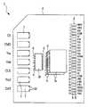
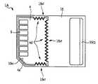
상기 메모리 카드(1)의 베이스 기판(4) 상에 실장된 2매의 칩(5a, 5a)은 동일한 외형 치수를 갖고, 동일기억 용량의 플래시 메모리(EEPROM)가 형성되어 있다. 이들 칩(5a, 5a)은 한쪽 상부에 다른 쪽을 정합시킨 상태로 베이스 기판(4) 상에 실장되어 있다. 하층의 칩(5a)은 베이스 기판(4) 상면에 접착제 등으로 접합되어 있고, 상층의 칩(5a)은 하층의 칩(5a)의 상면에 접착제 등으로 접합되어 있다. 한 편, 컨트롤러용 칩(5b)은 메모리용(1)의 칩(5a) 근방의 베이스 기판(4) 상에 실장되어 있고, 마찬가지로 접착제 등에 의해 베이스 기판(4)의 상면에 접합되어 있다. 이들 3매의 칩(5a, 5a, 5b)은 모두 그 주면(소자 형성면)을 위를 향한 상태로 베이스 기판(4)에 실장되어 있다.The two
플래시 메모리(EEPROM)가 형성된 2매의 칩(5a, 5a) 각각의 주면에는 그 1변을 따라 복수의 본딩 패드가 일렬로 형성되어 있다. 즉, 메모리용 칩(5a)은 소자 형성면의 주변부에 본딩 패드를 형성하고, 또한 이들 본딩 패드의 1변을 따라 일렬로 배치하는 한쪽 변 패드 방식을 채용하고 있다. 한편, 컨트롤러용 칩(5b)의 주면에는, 예를 들면 대향하는 두개의 긴 변을 따라 복수의 본딩 패드가 일렬씩 형성되어 있다.On the main surface of each of the two
2매의 칩(5a, 5a)은 상호 동일 방향을 향한 상태로 중첩되어 있고, 한쪽의 칩(5a)의 본딩 패드와 다른 쪽의 칩(5a)의 본딩 패드가 근접하여 배치되어 있다. 또한, 상층의 칩(5a)은, 그 일부가 하층의 칩(5a)의 1변에 평행한 방향(X 방향) 및 이것에 직교하는 방향(Y 방향)으로 어긋난 상태로 배치되어 있다.The two
상기 칩(5a, 5b)의 근방의 베이스 기판(4) 위에는 복수의 전극이 형성되어 있고, 각각의 칩(5a, 5a, 5b)의 본딩 패드와 대응하는 전극이 금(Au) 등으로 이루어지는 본딩 와이어(6)를 통해 전기적으로 접속되어 있다. 칩(5a)의 본딩 패드에는 상기 전극 및 전극에 전기적으로 접속된 베이스 기판(4)의 배선을 통해, 베이스 기판(4)의 일주면의 일단에 형성된 접속 단자(7) 및 타단에 형성된 테스트 패드(8)에 전기적으로 접속되어 있다. 접속 단자(7)는, 이 메모리 카드(1)를 상기 전자 기기에 장착할 때의 접속 단자로서 사용되고, 베이스 기판(4)의 하면의 외부 접속 단자(9)에 관통 홀(10)을 통해 전기적으로 접속되어 있다. 또한, 테스트 패드(8)는 이 메모리 카드(1)의 조립 공정 등에서, 전기적 특성을 측정하기 위해 사용된다. 이러한 칩(5a, 5b), 본딩 와이어(6) 및 베이스 기판(4)의 부품 탑재면의 대부분(접속 단자(7) 및 테스트 패드(8) 및 그 배치 영역의 주변을 제외)은, 예를 들면 에폭시계의 수지 등으로 이루어지는 밀봉 수지(11)로 덮도록 피복되어 있다.A plurality of electrodes are formed on the
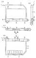
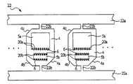
이어서, 상기 어댑터(2)에 대하여 설명한다. 도 7의 (a)는 어댑터(2)의 표면측의 평면도이고, 도 7의 (b)는 도 7의 (a)의 어댑터(2)의 측면도이며, 도 7의 (c)는 도 7의 (a)의 어댑터(2)의 전면도, 도 7의 (d)는 도 7의 (a)의 어댑터(2)의 이면측의 평면도, 도 7의 (e)는 도 7의 (a)의 어댑터(2)의 갈고리부(2b) 및 지지부(2c)의 주요부 확대 단면도를 도시하고 있다.Next, the
어댑터(2)는 수지 재료라도 형성 가능하지만, 강성이 더 높은데, 예를 들면 스테인레스, 티탄(Ti), 철(Fe) 또는 철을 포함하는 합금 등과 같은 금속판에 의해 구성되어 있다. 어댑터(2)의 재료로서 스테인레스를 선택한 경우에는 내부식성이 높으므로, 그 표면에 도금 등과 같은 표면 처리를 실시할 필요가 없다. 따라서, 형성이 용이하다. 또한, 비용을 저감시킬 수 있다. 한편, 어댑터(2)의 재료로서 철 등을 선택한 경우에는 그 표면에 도금 처리를 실시함으로써, 내부식성을 향상시킬 수 있다.The
또한, 어댑터(2)의 오목부(2a)는 어댑터(2)의 길이 방향의 양단이 단면 대략 U자 형상이 되도록 절곡시킴으로써 형성되어 있다. 이 때문에, 어댑터(2)는 그 두 께 방향으로 어느 정도의 빈 영역을 갖고 있다. 어댑터(2)를 중공형상으로 형성할 수도 있다.Moreover, the recessed
이와 같이, 본 실시예에서 어댑터(2)는 1매의 금속판을 절곡시키거나, 그 금속판에 홈(2d)이나 구멍(2e)을 형성함으로써 형성되어 있다. 즉, 정밀 가공이 필요한 금속의 절삭 기술 등을 이용하지 않는다. 또한, 부품 점수가 적다. 따라서, 어댑터(2)의 비용을 저감시킬 수 있다.Thus, in this embodiment, the
어댑터(2)에는, 그 전면으로부터 어댑터의 짧은 방향(도 7의 (a), 도 7의 (d)의 상하 방향)을 따라 그 짧은 방향의 도중 평면 위치까지 평행하게 연장되는 2개의 상기 홈(2d)이 띠형상으로 형성되어 있다. 이 2개의 홈(2d)에 평면적으로 끼워지는 부분(어댑터(2)의 길이 방향 중앙)에, 상기 지지부(2c)가 형성되어 있다. 지지부(2c)의 시단은, 어댑터(2)와 일체가 되어 접합되어 있다. 지지부(2c)의 타단에는, 상기 갈고리부(2a)가 일체로 형성되어 있다. 지지부(2c)는, 판 스프링(탄성체)으로서의 기능을 갖고 있으며, 평면적으로는 구형으로 형성되고, 또한 단면적으로는 어댑터(2)의 표면에서 이면을 향하여 점차로 절곡시키도록, 즉 휘어짐을 갖게 한 상태로 성형되어 있다. 이와 같이, 지지부(2c)에 휘어짐을 갖게 함으로써 탄성력의 향상과, 탄성체로서의 내구성의 향상을 도모하고 있다. 이와 같이, 지지부(2c)는 그 길이가 적절한 탄성을 갖게 하기 위한 길이로 설계되어 있는 것이 바람직하다.The
또한, 어댑터(2)의 배면측 근방에는, 구멍(2e)이 개구되어 있다. 상기 메모리 카드(1)에 어댑터(2)를 장착한 상태로, 이것을 전자 장치에 장착한 후, 그 메모 리 카드(1)를 전자 장치로부터 추출할 때에, 그 추출이 잘 이루어지지 않을 때에는, 이 구멍(2e)에 갈고리 혹은 공구를 걸어 메모리 카드(1)를 추출하면 된다. 구멍(2e)은 구멍 대신에 홈 등의 조임 형상이라도 가능하다.In addition, the
도 8은, 상기 메모리 카드(1)에 상기 어댑터(2)를 장착한 상태를 도시하고 있다. 도 8의 (a)는 그 메모리 카드(1) 및 어댑터(2)의 표면의 평면도, 도 8의 (b)는 도 8의 (a)의 측면도, 도 8의 (c)는 도 8의 (a)의 이면의 평면도를 각각 도시하고 있다. 또한, 도 9는, 비교를 위해 상기 풀 사이즈의 메모리 카드(50)를 도시하고 있다. 도 9의 (a)는 메모리 카드(50) 표면의 평면도, 도 9의 (b)는 그 측면도, 도 9의 (c)는 그 이면의 평면도를 각각 도시하고 있다. 또한, 도 10의 (a)는 메모리 카드(1)의 어댑터 갈고리 장착부(3b)와, 어댑터(2)의 갈고리부(2b)와의 접합부의 단면도를 도시하고, 도 10의 (b)는 메모리 카드(1)의 어댑터 장착부(3a)와, 어댑터(2)의 오목부(2a)와의 접합부의 단면도를 도시하고 있다.8 shows a state in which the
어댑터(2)는, 그 오목부(2a) 내에 메모리 카드(1)의 어댑터 장착부(3a)가 끼워지고, 또한 어댑터(2)의 지지부(2c) 선단의 갈고리부(2b)가 메모리 카드(1)의 어댑터 갈고리 장착부(3b)의 홈부(3b2) 내에 끼워진 상태로, 메모리 카드(1)에 장착되어 있다. 특히, 어댑터(2)의 지지부(2c)는 메모리 카드(1)의 표면측으로부터 이면측으로 들어가는 상태로 메모리 카드(1)에 장착되어 있다. 메모리 카드(1)에 어댑터(2)를 장착함으로써, 풀 사이즈의 메모리 카드(50)와 동등한 치수(예를 들면 32㎜×24㎜×1.4㎜)로 할 수 있다. 따라서, 상기 소형 전자 장치에 사용 가능한 하프 사이즈의 메모리 카드(1)를, 풀 사이즈의 메모리 카드(50)용 상기 대형 전자 장치에 사용할 수 있다. 즉, 하프 사이즈의 메모리 카드(1)의 범용성을 높일 수 있게 되어 있다.As for the
어댑터(2)의 갈고리부(2b)는, 도 10의 (a)의 상부 방향, 즉 캡(3)에 대향하는 방향으로 탄성력을 갖는 상태로, 메모리 카드(1)의 어댑터 갈고리 장착부(3a)의 홈부(3b2) 내에 확실히 끼워져 있다. 이에 따라, 메모리 카드(1)와 어댑터(2)를 확실하게 결합하는 것이 가능하게 되어 있다. 또한, 어댑터(2)의 오목부(2a)에는 메모리 카드(1)의 어댑터 장착부(3a)가 끼워진다. 이에 따라, 메모리 카드(1)와 어댑터(2)를 안정적으로 결합할 수 있게 되어 있다.The
메모리 카드(1)로부터 어댑터(2)를 착탈할 때는, 어댑터(2)의 지지부(2c)를 어댑터(2)의 표면측으로부터 이면의 방향으로 눌러, 지지부(2c)의 선단의 갈고리부(2b)를 메모리 카드(1)의 어댑터 갈고리 장착부(3b)로부터 분리하면 된다. 따라서, 한쪽 손으로도 간단히 어댑터(2)를 착탈할 수 있으며, 그 착탈 작업을 매우 용이하게 행할 수 있다. 이 때문에, 이 장착 시에 메모리 카드(1)의 표면에서 관찰되는 지지부(2c)의 길이는 사람의 손가락이 들어갈 정도가 바람직하다. 또, 지지부(2c)는 상기한 바와 같이 탄성을 갖고 있으므로, 어댑터(2)의 착탈 후에는 원래 형상으로 되돌아가게 되어 있다.When attaching and detaching the
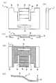
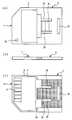
이어서, 상기 메모리 카드(1)의 캡(3)을 형성할 때에 이용하는 금형의 일례를 설명한다. 도 11은, 그 금형(15)의 단면도이고, 도 5와 동일한 개소의 단면도를 도시하고 있다. 또한, 도 12는, 도 11의 주요부 확대 단면도이고, 도 12(a)는 캡(3)의 배면측에서의 도 5의 (b)와 동일한 개소의 단면도, 도 12의 (b)는 캡(3)의 배면측에서의 어댑터 장착부(3a)에 대응하는 개소의 단면도, 도 12의 (c)는 캡(3)의 전면측에서의 도 5와 동일한 개소의 단면도를 도시하고 있다.Next, an example of the metal mold | die used when forming the
하형(15a)과 상형(15b)이 중첩된 부분에, 캡(3)을 성형하기 위한 캐비티(15c)가 형성되어 있다. 본 실시예에서는, 이 캐비티(15c)에 면하는 금형(15)(하형(15a) 및 상형(15b))의 각부의 각도 α1∼α11 등이 90°또는 그 이상으로 되어 있다(도 12 참조). 이에 따라, 캡(3)의 성형을 용이하게 할 수 있다. 만약, 상기 각부 α1∼α11 등이 90°보다 작으면, 캡(3)의 성형 후, 금형(15)으로부터 캡(3)을 박리하는 것이 어렵게 되어, 캡(3)을 1개씩 형성하거나, 특별한 금형 구조가 필요해지므로, 비용이 상승하게 된다. 이것에 비하여, 본 실시예에서는, 각도 α1∼α11 등을 90°또는 그 이상으로 함으로써, 그와 같은 문제점이 생기지 않으므로, 양산이 가능하게 되어있다. 또한, 특별한 금형 구조도 필요없다. 따라서, 메모리 카드(1)의 비용을 저감시킬 수 있다. 이러한 금형(15)으로 성형된 캡(3)의 표면, 측면 및 이면 각부의 각도는 90°또는 그 이상이 된다. 또한, 본 실시예에서는 캡(3)의 내측면을 형성하는 하형(15a)측에서의 캐비티(15c)의 깊이(거의 두께 d5+d6)가 캡(3)의 외측 표면을 형성하는 상형(15b) 측에서의 캐비티(15c)의 깊이(거의 두께 d7과 동등)보다도 깊게 되어 있다. 그리고, 두께 d6에 상당하는 부분에, 대부분이 하형(15a) 측에 수지 유입용 게이트가 형성된다. 하형(15a) 측의 캐비티(15c)의 깊이가 더 깊은 것은, 하형(15a) 측의 캐비티(15c) 내측(저면측)이 요철 및 단차가 더 많으며, 어느 정도의 용량이 없으면 수지를 잘 충전할 수 없기 때문이다. 또한, 두께 d5∼d7에서는, 두께 d6가 가장 치수가 크다. 이것은, 게이트에 서 캐비티(15c) 내에의 수지의 충전성을 향상시키기 위해서이다. 즉, 이 두께 d6이, 너무 얇으면 게이트를 통하여 캐비티(15c) 내에 수지를 유입시킬 수 없게 되기 때문이다. 여기서는, 두께 d5는 예를 들면 0.5㎜ 정도, 두께 d6은 예를 들면 0.6㎜ 정도, 두께 d7은 예를 들면 0.3㎜ 정도로 되어 있다.In the part where the lower mold |
본 실시예에서는, 이러한 금형(15)의 캐비티 내에 수지를 충전함으로써 캡(3)을 성형한 후, 그 캡(3)을 칩(5a, 5b)이 탑재된 베이스 기판(4)의 부품 탑재면을 덮도록 피복하고, 상기한 메모리 카드(1)를 제조한다.In the present embodiment, after the
이어서, 본 실시예의 반도체 장치의 조립 방법의 일례를 설명한다. 도 13은, 이것을 설명하기 위한 도면이며, 도 13의 (a)는 메모리 카드(1)의 전체 평면도, 도 13의 (b)는 메모리 카드(1)의 베이스 기판(4)을 풀 사이즈의 메모리 카드에 내장하여 사용한 경우의 전체 평면도를 각각 도시하고 있다. 해칭 표시된 부분이 베이스 기판(4)의 평면을 도시하고 있다.Next, an example of the assembly method of the semiconductor device of a present Example is demonstrated. FIG. 13 is a diagram for explaining this, FIG. 13A is an overall plan view of the
본 실시예에서는, 하프 사이즈의 메모리 카드(1)의 조립에 사용한 베이스 기판(4)(칩(5a) 등이 이미 실장된 상태의 베이스 기판(4))을, 풀 사이즈의 메모리 카드(1A)에 그대로 사용한다. 즉, 평면 사이즈가 다른 메모리 카드(1, 1A)의 부분을 공유시키도록 한다.In this embodiment, the base substrate 4 (
메모리 카드의 비용의 대부분은 베이스 기판(4)의 비용으로 차지되므로, 베이스 기판(4)의 비용을 저감시키는 것이 메모리 카드(1)의 비용을 저감시키는 데에 있어서 효과적이다. 그러나, 베이스 기판(4)을 하프 사이즈의 메모리 카드(1)와 풀 사이즈의 메모리 카드(1A)로 따로따로 제조한 경우, 각각 별개의 제조 공정, 제 조 장치 및 인원 등이 필요해지므로, 베이스 기판(4)의 비용의 증대를 초래하고, 메모리 카드의 비용이 비싸진다. 이것에 대하여, 메모리 카드(1, 1A)의 베이스 기판(4)을 공유시킴에 따라, 하프 사이즈와 풀 사이즈로 베이스 기판(4)의 제조 공정이나 제조 장치 혹은 인원을 별개로 설치할 필요가 없어지므로, 메모리 카드(1, 1A)의 비용을 대폭 저감시킬 수 있게 된다.Since most of the cost of the memory card is accounted for by the cost of the
이러한 조립 방법을 채용한 경우, 도 13의 (b)에 도시한 바와 같이 풀 사이즈의 메모리 카드(1A)에는 그 캡(16)의 평면적의 절반 또는 그 이하의 평면적의 베이스 기판(4)이 장착된다.In the case of adopting such an assembly method, as shown in Fig. 13B, the full-
(실시예 2)(Example 2)
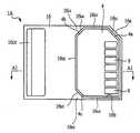
도 14는 본 발명의 다른 실시예인 반도체 장치 및 보조 기구의 사시도, 도 15의 (a), (b)는 도 14의 반도체 장치의 표면측 및 이면측의 외관을 도시한 사시도, 도 16의 (a)는 도 14의 반도체 장치의 표면측의 평면도, 도 16의 (b)는 도 16의 (a)의 반도체 장치의 측면도, 도 16의 (c)는 도 16의 (a)의 반도체 장치의 배면도, 도 16의 (d)는 도 16의 (a)의 반도체 장치의 이면측의 평면도, 도 17의 (a)는 도 14의 반도체 장치 및 보조 기구의 표면의 평면도, 도 17의 (b)는 도 17의 (a)의 측면도, 도 17의 (c)는 도 17의 (a)의 이면의 평면도를 각각 도시하고 있다.14 is a perspective view of a semiconductor device and an auxiliary mechanism according to another embodiment of the present invention; FIGS. 15A and 15B are perspective views showing the appearance of the front and back sides of the semiconductor device of FIG. a) is a plan view of the surface side of the semiconductor device of FIG. 14, FIG. 16B is a side view of the semiconductor device of FIG. 16A, and FIG. 16C is a view of the semiconductor device of FIG. 16D is a plan view of the back side of the semiconductor device of FIG. 16A, FIG. 17A is a plan view of the surfaces of the semiconductor device and the auxiliary mechanism of FIG. 14, and FIG. ) Is a side view of FIG. 17A, and FIG. 17C shows a plan view of the rear surface of FIG. 17A, respectively.
본 실시예는 메모리 카드(1)와 어댑터(2)와의 결합 개소의 형상이 상기 실시예 1과 다른 것외에는 상기 실시예 1과 동일하다. 즉, 메모리 카드(1)의 어댑터 장착부(3a) 측면이 메모리 카드(1) 측면과 동일 평면이 되도록 형성되어 있다. 즉, 어댑터 장착부(3a)의 측면 부분이 우묵하게 들어가지 않는다. 또한, 이 어댑터 장착부(3a)에 끼워지는 어댑터(2)의 오목부(2a)의 부분에는, 메모리 카드(1)의 측면에도 상기 어댑터 장착부(3a)의 측면 부분이 들어갈 수 있는 홈(2a1)이 부분적으로 형성되어 있다.The present embodiment is the same as that of the first embodiment except that the shape of the coupling portion between the
이러한 경우라도, 도 17에 도시한 바와 같이 메모리 카드(1)와 어댑터(2)와의 결합 측면에 요철이나 문제점을 발생시키지 않고 확실하게 한 상태로 메모리 카드(1)에 어댑터(2)를 장착할 수 있다.Even in such a case, as shown in FIG. 17, the
이러한 본 실시예에서도 상기 실시예 1과 마찬가지의 효과를 얻을 수 있다.In this embodiment as well, the same effects as in the first embodiment can be obtained.
(실시예 3)(Example 3)
도 18은 본 발명의 또 다른 실시예의 반도체 장치의 이면측의 평면도를 도시하고 있다. 본 실시예에서는, 메모리 카드(1)의 배면측에서 어댑터 장착부(3a)의 근방에 복수의 접속 단자(17)가 메모리 카드(1)의 길이 방향을 따라 규칙적으로 나열되어 배치되어 있다. 접속 단자(17)는 베이스 기판(4)의 이면측에 설치되어 있고, 베이스 기판(4)의 배선을 통하여 베이스 기판(4) 상에 형성된 메모리 회로와 전기적으로 접속되어 있다. 이 접속 단자(17)는 상기 메모리 회로의 테스트용 또는 기능 추가용의 단자이다.18 is a plan view of the back side of a semiconductor device of still another embodiment of the present invention. In this embodiment, a plurality of
(실시예 4)(Example 4)
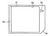
우선, 본 발명자가 검토한 기술에서 본 발명자가 처음으로 발견한 과제에 대하여 도 19∼도 23에 의해 설명한다.First, the subject which this inventor discovered for the first time by the technique examined by this inventor is demonstrated by FIGS. 19-23.
도 19 및 도 20은 상기 베이스 기판(4)의 표면(부품 탑재면) 및 이면(외부 접속 단자 형성면)의 평면도를 각각 도시하고 있다. 베이스 기판(4)은 평면 구형 으로 형성되어 있고, 그 하나의 각부 해당 개소는 각이 깍여 모따기부(제3 모따기부 : 4a)가 형성되어 있다. 모따기부(4a)는 메모리 카드의 전면 선단(장착단)에 형성된 인덱스용의 모따기에 따르도록 형성되어 있다.19 and 20 show plan views of the front surface (part mounting surface) and the rear surface (external connection terminal forming surface) of the
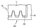
도 21 및 도 22는 본 발명자가 검토한 상기 풀 사이즈의 메모리 카드용 캡(제1 케이스 본체 : 16)의 표면 및 이면의 평면도를 각각 도시하고 있다. 이 캡(16)은, 상기 하프 사이즈용 캡(3)과 마찬가지의 수지 등에 의해 형성되어 있다. 캡(16)에서 메모리 카드의 전면측의 각부 한쪽에는, 상기 인덱스용 모따기부(제2 모따기부 : 16a)가 형성되어 있다. 이 모따기부(16a)는 풀 사이즈의 메모리 카드의 장착 방향을 인식하기 쉽게 하는 등의 관점에서 설치되어 있다.21 and 22 show plan views of the front and rear surfaces of the cap for the full-size memory card (first case main body 16) examined by the present inventors, respectively. The
또한, 캡(16)의 이면에서 상기 메모리 카드의 전면측에는 홈(16b)이 형성되어 있다. 이 홈(16b)은 베이스 기판(4)을 캡(16)에 설치하기 위한 홈이며, 캡(16)의 선단 근방에서 캡(16)의 길이 방향의 절반보다도 약간 짧은 위치까지 점유하도록 형성되어 있다. 홈(16b)의 평면적인 형상 및 치수는 베이스 기판(4)을 넣기 좋게 끼울 수 있도록 베이스 기판(4)과 동일 평면 형상으로, 또한 베이스 기판(4)보다도 약간 큰 평면 치수로 형성되어 있다. 따라서, 홈(16b)에서, 캡(16)의 전면측의 한쪽 각부는 캡(16)의 모따기부(16a)를 따르도록 각이 깍여 모따기부(16b1)가 형성되어 있다. 또한, 홈(16b)의 두개의 긴 변 중 캡(16)의 길이 방향 중앙측에 형성되어 있는 긴 변과, 홈(16b)의 두개의 짧은 변이 직각으로 교차하고 있다. 또, 홈(16b)의 영역내에서 외주에는 그 내측보다도 약간 두껍고, 또한 홈(16b)의 외측보다는 약간 얇은 단차부(16e)가 형성되어 있다. 이 단차부(16e)에 새겨진 복수 의 핀 자국(16f)은 캡(16)을 금형으로 성형한 후에 금형으로부터 추출할 때에 에젝터 핀이 접촉한 자국을 도시하고 있다.In addition, a
또한, 이 캡(16)의 표면 및 이면에서 배면측 근방에는, 카드 추출 홈(16c1, 16c2)이 형성되어 있다. 이 카드 추출 홈(16c1, 16c2)은, 상기 실시예 1에서 설명한 카드 추출 홈(3c)(도 1 등 참조)과 마찬가지의 기능을 갖는 홈이다. 이면측 홈부(16c2)의 깊이는 표면측의 카드 추출 홈(16c1)보다도 깊게 형성되어 있다. 이 카드 추출 홈(16c1, 16c2)은 어느 한쪽을 설치하기만 해도 된다. 또한, 캡(16)의 표면에서 전면 근방측에는 풀 사이즈의 메모리 카드를 상기 전자 장치에 장착할 때의 삽입 방향을 나타내는 평면 삼각형 형상의 마크(16d)가 형성되어 있다. 또한, 캡(16) 표면의 대부분의 부분은 평면각환의 장방형의 얕은 오목부(16g)가 형성되어 있다. 이 오목부(16g)는 메모리 카드의 분류 등을 표시하는 등, 다양한 정보를 기재하기 위한 시일 등을 접착하기 위한 것이다.Further, card extraction grooves 16c1 and 16c2 are formed in the vicinity of the back side on the front and rear surfaces of the
도 23은, 도 19 및 도 20에 도시한 베이스 기판(4)을, 도 21 및 도 22의 캡(16)의 홈(16b)에 설치한 후 풀 사이즈의 메모리 카드(1A)의 이면의 평면도를 도시하고 있다. 베이스 기판(4)은 캡(16)의 길이 방향의 거의 한쪽측 절반의 영역에 들어가기 좋게 설치되어 있다.FIG. 23 is a plan view of the rear surface of the full-
그런데, 본 발명자는 도 23에 도시한 풀 사이즈의 메모리 카드(1A)에 대하여 구부러짐 강도 시험을 행하였다. 이 구부러짐 강도 시험은, 예를 들면 다음과 같다. 우선, 메모리 카드(1A)의 이면을 시험대의 상면을 향한 상태로 메모리 카드(1A)를 시험대 위에 싣는다. 이 때, 메모리 카드(1A)의 길이 방향의 양단 근방의 2 개소에서, 메모리 카드(1A)의 이면과 시험대의 상면 사이에 지지 부재를 개재시켜, 메모리 카드(1A)의 이면과, 시험대의 상면 사이에 소정 치수의 간극이 형성되도록 한다. 이 상태로, 메모리 카드(1A)의 표면에서 길이 방향 중앙에 소정량의 하중을 가함으로써, 메모리 카드(1A)를 휘게 하여 파괴 강도를 평가한다.Incidentally, the present inventors conducted a bending strength test on the full-
본 발명자는 이 시험의 결과, 도 23에 도시한 바와 같은 메모리 카드(1A)는 풀 사이즈의 메모리 카드에서 베이스 기판과 캡과의 평면 치수가 같은 정도가 되는 구조의 것과 비교하여 구부러짐 강도가 약하고, 메모리 카드(1A)의 이면 중앙에서 캡(16)과 베이스 기판(4)과의 경계부(간극부)에서 베이스 기판(4)이 박리되거나, 캡(16)의 홈(16b)이 긴 변 중 캡(16)의 길이 방향 중앙측에 형성되어 있는 긴 변과 홈(16b)의 두개의 짧은 변이 직각으로 교차하는 부분을 기점으로 하여 캡(16)에 크랙이 생기기도 하는 등과 같은 문제점이 생기는 것을 처음으로 발견하였다.As a result of this test, the inventors of the present invention show that the
그래서, 본 실시예에서는 베이스 기판의 평면 치수가 캡의 평면 치수의 절반 정도가 되는 풀 사이즈의 메모리 카드에 있어서, 상기 구부러짐 강도가 향상하는 구조로 하였다. 구체적으로는 예를 들면 이하와 같다.Therefore, in the present embodiment, the bending strength is improved in the full size memory card in which the planar dimension of the base substrate is about half the planar dimension of the cap. Specifically, it is as follows, for example.
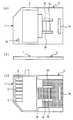
도 24 및 도 25는 본 실시예 4의 베이스 기판(4)의 표면(부품 탑재면) 및 이면(외부 접속 단자 형성면)의 평면도를 각각 도시하고 있다. 본 실시예 4의 베이스 기판(4)에서는 상기 모따기부(4a) 외에 두개의 각부 해당 개소의 각이 깍여 모따기부(제1 모따기부 : 4b, 4c)가 형성되어 있다. 이 모따기부(4b, 4c)는 모따기부(4a)보다는 작게 모따기되어 이루어지며, 상호 좌우 대칭이 되도록 동일한 크기 및 형상으로 형성되어 있다. 이 외에는 상기 실시예 1, 도 19 및 도 20 등에서 설 명한 것과 동일하다.24 and 25 show plan views of the front surface (part mounting surface) and the rear surface (external connection terminal formation surface) of the
도 26 및 도 27은, 도 24 및 도 25에 도시한 베이스 기판(4)을 탑재하는 풀 사이즈의 메모리 카드용의 캡(16)에서의 표면 및 이면(베이스 기판 장착면)의 평면도를 각각 도시하고 있다. 본 실시예 4의 캡(16)은 베이스 기판(4)을 장착하는 홈(제1 홈 : 16b)의 형상이 상기한 것과 다르다. 그 외의 구성은, 상기 실시예 1, 도 21 및 도 22에서 설명한 것과 동일하다. 즉, 본 실시예 4에서는 홈(16b)의 평면적인 형상 및 치수는, 도 24 및 도 25에 도시한 베이스 기판(4)을 들어가기 좋게 끼우는 것이 가능하도록 그 베이스 기판(4)과 동일 평면 형상으로, 또한 베이스 기판(4)보다도 약간 큰 평면 치수로 형성되어 있다. 따라서, 이 경우의 홈(16b)의 두개의 긴 변 중의 캡(16)의 길이 방향 중앙측에 형성되어 있는 긴 변(16b2)과, 홈(16b)의 두개의 짧은 변(16b3, 16b3)은 직각으로 교차하지 않으며, 그 본래 직교하는 부분은 각이 깍여 모따기부(제1 모따기부 : 16b4, 16b5)가 형성되어 있다. 즉, 홈(16b)은 그 긴 변(16b2) 및 짧은 변(16b3)의 상호간이, 이들에 대하여 비스듬히 교차하도록 배치된 모따기부(16b4, 16b5)를 통해 점차로 전환되도록 하는 구조로 되어 있다. 혹은 홈(16b)에서 캡(16)의 길이 방향 중앙측에 본래 형성되는 두개의 각부에 직각 이등변 삼각형 형상의 보강부(16h1, 16h2)가 직각부를 정합한 상태로 배치되어 있는 구조로 되어 있다. 이 모따기부(16b4, 16b5)는 모따기부(16a)보다는 작게 모따기되어 이루어지며, 상호 좌우 대칭이 되도록 동일한 크기 및 형상으로 형성되어 있다.26 and 27 show top views of the front and rear surfaces (base substrate mounting surface) of the
도 28은, 도 24 및 도 25에 도시한 베이스 기판(4)을, 도 26 및 도 27의 캡 (16)에 설치한 후의 풀 사이즈의 메모리 카드(1A)에서의 이면의 평면도를 나타내고, 도 29는 도 28의 A1-A1선의 단면도를 도시하고 있다. 본 실시예 4에서 베이스 기판(4)은 그 표면을 캡(16)의 이면의 홈(16b) 측을 향하며, 또한 베이스 기판(4)의 모따기부(4b, 4c)를 각각 홈(16b)의 모따기부(16b4, 16b5)로 대향시킨 상태로 홈(16b) 내에 장착되어 있다. 베이스 기판(4)은, 그 표면 외주부가 캡(16)의 홈(16b) 내에서의 단차부(16e)에 접촉한 상태로 지지되어 있다.FIG. 28 shows a plan view of the back surface of the full-
본 실시예 4에서는, 베이스 기판(4)과 홈(16b)과의 접촉 길이를 도 23에 도시한 경우보다도 길게 할 수 있으므로, 베이스 기판(4)과 캡(16)과의 접합 강도를 향상시킬 수 있다. 또한, 베이스 기판(4)에 모따기부(4b, 4c)를 설치하고, 또한 홈(16b)에 모따기부(16b4, 16b5)를 설치하여, 응력 집중하기 쉬운 직각부를 없앰으로써, 응력을 분산시킬 수 있다. 이들에 의해, 상기 구부러짐 강도 시험에 있어서, 베이스 기판(4)의 박리를 억제하거나 또는 방지할 수 있고, 또한 캡(16)에 크랙이 생기는 것을 억제하거나 또는 방지할 수 있다.In the fourth embodiment, since the contact length between the
또한, 상기 구부러짐 강도를 향상시키는 구조는, 다른 새로운 부재를 추가하는 것은 아니며, 베이스 기판(4)의 각부 및 캡(16)의 홈(16b)의 각부를 모따기하는 정도의 단순한 구조이며, 그 형성이 용이하다. 따라서, 생산성을 저해하지 않고 신뢰성이 높은 풀 사이즈의 메모리 카드(1A)를 제공할 수 있다.Moreover, the structure which improves the said bending strength does not add another new member, but is a simple structure of chamfering each part of the
또한, 본 실시예 4의 풀 사이즈의 메모리 카드(1A)는 정전 파괴 시험에서도 유리한 구조로 되어 있다. 이 정전 파괴 시험에서는, 메모리 카드(1A)를 시험 장치에 장착한 상태로, 배면측에서 정전기를 인가하는 것이다. 풀 사이즈의 메모리 카드에서, 베이스 기판과 캡과의 평면 치수가 같은 정도로 되는 구조에서는, 메모리 카드의 배면측의 근방까지 베이스 기판이 설치되어 있으므로, 메모리 카드의 배면측에서 전면측의 칩까지의 도전 경로의 거리가 짧다. 이것에 비하여, 본 실시예 4의 메모리 카드(1A)에서는, 그 배면에서 길이 방향은 거의 절반 정도까지는 절연성의 캡(16)으로 형성되어 있고, 그 배면측에서 전면측의 칩까지의 도전 경로의 거리가 길므로, 정전 파괴 시험에서 파괴가 생기기 어려운 구조로 되어 있다.In addition, the full
또한, 풀 사이즈의 메모리 카드(1A)에서, 베이스 기판(4)의 평면 치수가 캡(16)의 평면 치수의 절반 정도로 되어 있는 구조에서는 베이스 기판과 풀 사이즈의 캡과의 평면 치수가 같은 정도로 이루어지는 구조와 비교하여, 베이스 기판(4)의 면적 및 밀봉 수지(11)의 체적을 작게 할 수 있으므로, 풀 사이즈의 메모리 카드(1A)를 가볍게 할 수 있다. 특히, 본 실시예 4의 메모리 카드(1A)에서는 상기한 바와 같이 베이스 기판(4)의 각부를 더 모따기하고 있으므로, 경량화를 추진할 수 있다. 따라서, 풀 사이즈의 메모리 카드(1A)의 휴대성을 향상시킬 수 있게 된다.In the full
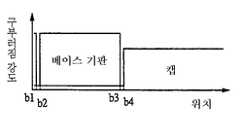
도 30∼도 32는, 도 23에 도시한 메모리 카드(1A)의 구부러짐 강도 시험의 결과의 설명도를 도시하고 있다. 이 구조의 메모리 카드(1A)에서는 캡(16)의 길이 방향의 거의 중앙에서의 베이스 기판(4)과 캡(16)과의 경계 개소(위치 b3, b4)에서 구부러짐 강도가 급격히 게다가 구형으로 크게 저하하고 있는 것을 알 수 있다. 또, 부호 b1∼b4는, 도 30∼도 32에서 상호간의 위치 관계를 알 수 있는 위치를 도시하고 있다.30 to 32 show explanatory diagrams of the results of the bending strength test of the
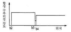
한편, 도 33∼도 35는 본 실시예 4의 도 28 등에 도시한 메모리 카드(1A)의 구부러짐 강도 시험의 결과의 설명도를 도시하고 있다. 본 실시예 4의 메모리 카드(1A)에서는 캡(16)의 길이 방향의 거의 중앙에서의 베이스 기판(4)과 캡(16)과의 경계 개소(위치 b5, b6, b4)에서 구부러짐 강도가 저하하여 비교적 완만함과 동시에, 그 최저값이 도 31 및 도 32의 경우보다도 높은 값으로 되어 있는 것을 알 수 있다. 즉, 풀 사이즈의 메모리 카드(1A)의 구부러짐 강도를 향상시킬 수 있다.33 to 35 show explanatory diagrams of the results of the bending strength test of the
이어서, 본 실시예 4의 풀 사이즈의 메모리 카드(1A)의 치수 상의 정의 등에 대하여 도 36 및 도 37에 의해 설명한다.Next, definitions and the like on the dimensions of the full-
도 36은 본 실시예 4의 캡(16)의 이면의 평면도를 도시하고 있다. 홈(16d)의 짧은 방향의 길이(즉, 거의 베이스 기판(4)의 짧은 방향의 치수) X1은, 캡(16)의 길이 방향에서의 전체 길이 X2의 절반보다도 작다(X1<X2/2). 이것은, 베이스 기판(4)을 풀 사이즈와 하프 사이즈와의 양방으로 사용 가능하게 하기 위해서이다. 즉, 폭 X1을 전체 길이 X2의 절반이나 그것보다 길게 하면, 그 베이스 기판을 상기 실시예 1에서 설명한 하프 사이즈의 메모리 카드(1)에 사용할 수 없게 되기 때문이다. 길이 X1은, 예를 들면 14.5㎜ 정도, 전체 길이 X2는 예를 들면 32㎜ 정도이다.36 shows a plan view of the back surface of the
또한, 본 실시예 4에서는 모따기부(16b4, 16b5)에서, 캡(16)의 길이 방향의 길이 X3과, 캡(16)의 짧은 방향의 길이 Y1을 동일하게 하고 있다(X3=Y1). 따라서, 각도θ는 45°정도이다. 이론적으로는 이 경우가 각부 영역에서의 구부러짐 강도를 전체적으로 향상시킬 수 있기 때문이다. 또한, 본 발명자의 검토에 따르면, Y1>X3에서도 구부러짐 강도 상의 좋은 결과를 얻을 수 있다. 길이 X3, Y1은 예를 들면 2㎜ 정도이다.In the fourth embodiment, the lengths X3 in the longitudinal direction of the
또한, 모따기부(16a)의 길이 L2는 길이 X3, Y1보다도 길다(L2>X3, Y1). 이것은, 길이 X3, Y1을 너무 크게 하면, 베이스 기판(4)의 면적이 작아져, 칩을 탑재할 수 없게 되기 때문이다. 길이 L2는, 예를 들면 5.66㎜ 정도이다.The length L2 of the chamfered
또한, 이 길이 X3, Y1은 두께 d8, d9, d10보다도 큰 (X3, Y1>d8, d9, d10). 이것은, 길이 X3, Y1이 두께 d8∼d10보다 작으면 모따기량이 너무 작고 상기 구부러짐 강도를 충분히 얻을 수 없기 때문이다. 두께 d8은, 예를 들면 1㎜ 정도, 두께 d9, d10은 예를 들면 0.6㎜ 정도이다.In addition, this length X3, Y1 is larger than thickness d8, d9, d10 (X3, Y1> d8, d9, d10). This is because when the lengths X3 and Y1 are smaller than the thicknesses d8 to d10, the chamfering amount is too small and the bending strength cannot be sufficiently obtained. Thickness d8 is about 1 mm, for example, and thickness d9 and d10 are about 0.6 mm, for example.
또한, 도 37은 본 실시예 4의 메모리 카드(1A)의 주요부 확대 단면도를 도시하고 있다. 메모리 카드(1A)의 총 두께는 캡(16)의 두께 d11에 상당한다. 이 두께 d11은 두께 d12와 동일하거나, 그 이상이다(d11≥d12). 두께 d12는 캡(16)의 표면에서 베이스 기판(4)의 이면까지의 두께이다. 상기한 치수 규정의 이유는, 이 두께 d12가 두께 dl1보다도 두꺼워지면 메모리 카드의 규격에 안 맞게 되기 때문이다. 깊이 d13은, 홈(16b)의 깊이를 도시하고 있다. 두께 d11은 예를 들면 1.4㎜ 정도이다. 두께 d12는 예를 들면 1.4㎜ 정도이거나 또는 그 이하이다. 깊이 d13은 예를 들면 1.04㎜ 정도, 두께 d14는 예를 들면 0.28㎜ 정도이다.37 shows an enlarged sectional view of the main part of the
이어서, 도 26∼도 29 등에 도시한 풀 사이즈용의 캡(16)의 형성할 때에 이용하는 금형의 일례를 도 38에 의해 설명한다. 도 38은, 그 금형(15)의 단면도이다. 그 구조는 상기 실시예 1의 도 11 및 도 12의 (a), (c)에서 설명한 것과 거의 동일하다. 다른 것은, 캐비티(15c)의 길이 방향의 길이가, 도 15에서 설명한 것보 다도 긴 것이다. 즉, 캐비티(15c)의 길이 방향의 거의 중앙에서 캡(16)의 배면부를 형성하는 부분까지의 길이가 도 11 및 도 12에서 도시한 보다도 길다.Next, an example of the metal mold | die used at the time of forming the
이어서, 본 실시예 4의 베이스 기판(4)에서의 칩의 배치예를 도 39 및 도 40에 의해 설명한다. 도 39 및 도 40은, 본 실시예 4에서의 베이스 기판(4)의 표면(부품 탑재면)의 평면도를 도시하고 있다.Next, examples of arrangement of chips in the
본 실시예 4에서는, 베이스 기판(4)의 표면에 하나의 메모리용 칩(5a) 및 하나의 컨트롤러용 칩(5b) 등이 탑재되어 있다. 이 두개의 칩(5a, 5b)은, 베이스 기판(4)의 길이 방향(즉, 복수의 외부 접속 단자(9)(도 25, 도 28 참조)가 배치되는 방향)을 따라 배열하여 배치되어 있다. 상대적으로 큰 메모리용 칩(5a)은 인덱스측의 모따기(4a)에서 먼 위치에 떨어져 배치되어 있다. 한편, 상대적으로 작은 컨트롤러용 칩(5b)은 인덱스측의 모따기부(4a)에 가까운 측에 배치되어 있다. 이러한 배치에 의해, 조밀하고 대용량인 메모리 카드를 실현할 수 있다.In the fourth embodiment, one
상기 메모리용 칩(5a)에는, 예를 들면 16M, 32 바이트의 메모리 용량의 메모리 회로가 형성되어 있다. 메모리용 칩(5a)이 컨트롤러용 칩(5b)보다도 정방형에 가까운 형상을 하고 있다. 메모리용 칩(5a)의 1변의 길이 L3은, 컨트롤러용 칩(5b)의 길이 방향으로 연장되는 1변의 길이 L4보다도 길게 형성되어 있다. 메모리용 칩(5a)의 주면에서 1변의 근방에는 그 1변을 따라 복수의 본딩 패드(20a)가 배치되어 있다. 메모리용 칩(5a)은 그 복수의 본딩 패드(20a)가 배치되어 있는 1변이, 베이스 기판(4)의 길이 방향 중앙측, 즉 컨트롤러용 칩(5b) 측에 배치되도록 탑재되어 있다. 이 본딩 패드(20a)는 본딩 와이어(6)를 통하여 베이스 기판(4)의 표면의 배선과 전기적으로 접속되어 있다.In the
한편, 컨트롤러용 칩(5b)의 주면에서, 두개의 긴 변의 근방에는 그 긴 변을 따라 복수의 본딩 패드(20b)가 배치되어 있다. 컨트롤러용 칩(5b)은 그 긴 변이 메모리용 칩(5a)의 복수의 본딩 패드(20a)가 배치되어 있는 1변에 대하여 거의 평행해지도록 베이스 기판(4)의 표면 상에 탑재되어 있다. 이 본딩 패드(20b)는 본딩 와이어(6)를 통하여 베이스 기판(4)의 표면의 배선과 전기적으로 접속되어 있다. 이러한 칩(5a, 5b)의 배치는, 상기 실시예 1∼3에도 적용할 수 있다.On the other hand, on the main surface of the
또, 베이스 기판(4)의 표면의 길이 방향의 선단측(모따기부(4a)가 형성된 측)에는, 금 도금 등에 의해 형성된 메탈층(21)이 형성되어 있다. 이 메탈층(21)은 칩(5a, 5b)을 밀봉할 때에 금형 게이트가 배치되는 부분이다. 즉, 밀봉 수지(11)(도 29 등 참조)를 형성할 때에는, 그 메탈층(21) 측으로부터 컨트롤러용 칩(5b)의 배치 영역을 통해 메모리용 칩(5a)의 배치 영역으로 수지가 흐르게 되어 있다.Moreover, the
이어서, 본 실시예 4의 반도체 장치의 조립 방법의 일례를 설명한다. 이 조립 공정은, 상기 실시예 1의 도 13에서 설명한 것과 동일하다. 여기서는, 그 조립 공정을 도 41의 흐름도에 따라 도 42∼도 46에 의해 설명한다. 또, 도 42∼도 46은 그 조립 공정 중에서의 베이스 기판(4)의 표면의 평면도이다.Next, an example of the assembly method of the semiconductor device of Example 4 is demonstrated. This assembling process is the same as that described in FIG. 13 of the first embodiment. Here, the assembling process will be described with reference to FIGS. 42 to 46 in accordance with the flowchart of FIG. 41. 42 to 46 are plan views of the surface of the
우선, 도 42에 도시한 바와 같은 베이스 기판 형성체(22)를 준비한다. 이 베이스 기판 형성체(22)의 프레임(22a)에는 이미 복수의 베이스 기판(4)이 각 베이스 기판(4)의 두개의 짧은 변 중앙에 접속된 미세한 연결부(22b)를 통해 접속되어 있다. 이 단계에서는, 프레임(22a), 연결부(22b) 및 베이스 기판(4)은 일체적으로 형성되어 있다. 또한, 베이스 기판(4)의 모따기부(4b, 4c)도 이미 형성되어 있다. 이어서, 도 43에 도시한 바와 같이 베이스 기판 형성체(22)의 각 베이스 기판(4)의 표면 상에 칩(5a, 5b)을 탑재한다(도 41의 공정 100). 이 때, 상대적으로 큰 메모리용 칩(5a)을 모따기부(4a)로부터 떨어진 곳에 탑재하고, 상대적으로 작은 컨트롤러용 칩(5b)을 모따기부(4a)에 가까운 곳에 탑재한다. 그 후, 베이스 기판(4) 및 칩(5a, 5b)의 배선, 전극(본딩 패드(20a, 20b)를 포함)의 표면을 청정화하기 위해, 예를 들면 플라즈마 클리닝 처리를 실시한다(도 41의 공정 101). 이 공정은, 얇게 형성되어 있는 금 도금층의 표면을 청정하게 함으로써, 이 공정에 계속되는 본딩 와이어 공정 시에 와이어와 금 도금층과의 접속 상태를 양호하게 하는 것을 주 목적으로 하고 있다.First, the base
이어서, 도 44에 도시한 바와 같이 각 베이스 기판(4)에서, 칩(5a, 5b)의 본딩 패드(20a, 20b)와 베이스 기판(4)의 배선이나 전극을 본딩 와이어(6)를 통하여 전기적으로 접속한다(도 41의 공정102). 이어서, 도 45에 도시한 바와 같이 각 베이스 기판(4)에서, 칩(5a, 5b) 및 본딩 와이어(6) 등을 트랜스퍼 몰드법에 의해 밀봉한다(도 41의 공정103). 상기 와이어 본딩 공정 후, 몰드 공정 전에 밀봉 수지(11)의 접착성을 향상시키는 관점에서 상기 클리닝 처리를 베이스 기판(4)에 실시해도 된다. 그 후, 도 46에 도시한 바와 같이 연결부(22b)를 절단함으로써, 베이스 기판(4)을 베이스 기판 형성체(22)로부터 분리한다(도 41의 공정104). 이와 같이 함으로서 베이스 기판(4)을 형성한다.Then, as shown in FIG. 44, in each
이어서, 풀 사이즈(FS)의 메모리 카드(1A)를 제조하는 경우에는, 상기 베이 스 기판(4)을 도 26 및 도 27에 도시한 캡(16)의 홈(16) 내에 설치하여 접착제 등으로 고정한다(도 41의 공정105A). 한편, 하프 사이즈(HS)(또는 레듀스 사이즈(RS))의 메모리 카드(1)를 제조하는 경우에는, 베이스 기판(4)을 상기 실시예 1의 도 1∼도 5 등에서 설명한 캡(3)의 이면의 홈(여기서의 홈의 평면 형상은, 도 27∼도 29에서 설명한 형상으로 형성되어 있음) 내에 설치하여 접착제 등으로 고정한다(도 41의 공정105B).Subsequently, in the case of manufacturing the full size
이와 같이 본 실시예에서는 하나의 베이스 기판(4)으로 풀 사이즈와 하프 사이즈의 2 종류의 메모리 카드(1, 1A)를 제조할 수 있다. 즉, 풀 사이즈와 하프 사이즈와의 메모리 카드(1, 1A)의 제조 공정 및 부재를 일부 공통화할 수 있으므로, 따로 제조한 경우와 비교하여 제조 공정의 간략화, 제조 시간의 단축 및 제조 비용의 저감이 가능해진다.As described above, in this embodiment, two types of
(실시예 5)(Example 5)
본 실시예 5에서는, 베이스 기판의 평면 치수가 캡의 평면 치수의 절반 정도가 되는 풀 사이즈의 메모리 카드에 있어서, 상기 구부러짐 강도를 향상시키는 구조의 변형예를 설명한다.In the fifth embodiment, a modification of the structure for improving the bending strength in a full-size memory card in which the planar dimension of the base substrate is about half the planar dimension of the cap will be described.
도 47은 본 실시예 5의 풀 사이즈의 메모리 카드(1A)에서의 이면의 평면도를 도시하고, 도 48은 도 47의 영역 Z1의 확대 평면도를 도시하고 있다. 본 실시예 5에서는, 베이스 기판(4)에서 풀 사이즈의 캡(16)의 길이 방향 중앙측에 위치하는 양 각부의 근방에 미세한 장방형 요철(4d)이 형성되고, 이것에 대응하는 캡(16)의 홈(16b)의 각부 근방에도 베이스 기판(4)의 미세한 요철(4d)에 잘 감압될 수 있도 록 미세한 장방형 요철(16b7)이 형성되어 있다. 이 미세한 요철(4d, 16b7)은, 도 47에서 좌우 대칭이 되도록 형성되어 있다. 이 외에는, 상기 실시예 1∼4에서 설명한 것과 동일하다. 상기 요철(4d, 16b7)은 홈(16b)의 긴 변(16b2) 및 이것에 대응하는 베이스 기판(4)의 긴 변측에 설치해도 된다.FIG. 47 shows a plan view of the back side of the full
본 실시예 5에서도, 상대적으로 강도가 약한 각부에서 베이스 기판(4)과 캡(16)과의 접촉 면적을 증대시킬 수 있으므로, 캡(16)의 크랙이나 베이스 기판(4)의 박리를 억제하거나 또는 방지할 수 있고, 상기 구부러짐 강도를 향상시킬 수 있게 되어 있다.Also in the fifth embodiment, since the contact area between the
(실시예 6)(Example 6)
본 실시예 6에서는, 베이스 기판의 평면 치수가 캡의 평면 치수의 절반 정도가 되는 풀 사이즈의 메모리 카드에 있어서, 상기 구부러짐 강도를 향상시키는 구조의 다른 변형예를 설명한다.In the sixth embodiment, another modification of the structure for improving the bending strength in a full-size memory card in which the planar dimension of the base substrate is about half the planar dimension of the cap will be described.
도 49는 본 실시예 6의 풀 사이즈의 메모리 카드(1A)에서의 이면의 평면도를 도시하고, 도 50은 도 49의 영역 Z2의 확대 평면도를 도시하고 있다. 본 실시예 6에서도 상기 실시예 5와 마찬가지로, 베이스 기판(4)의 각부 근방 및 그것에 대응하는 캡(16)의 홈(16b)의 각부 근방에 미세한 요철(4d, 16b7)이 형성되어 있다. 상기 실시예 5와 다른 것은, 각각의 미세한 요철(4d, 16b7) 측면에 테이퍼가 형성되어 있는 것이다. 이 경우, 베이스 기판(4)의 미세한 요철(4d)과, 캡(16)의 홈(16b)의 미세한 요철(4d)을 상기 실시예 5의 경우보다도 끼우기 쉽다. 이 외에는, 상기 실시예 1∼5에서 설명한 것과 동일하다. 상기 요철(4d, 16b7)은 홈(16b)의 긴 변(16b2) 및 이것에 대응하는 베이스 기판(4)의 긴 변측에 설치해도 된다.FIG. 49 shows a plan view of the back side of the full
(실시예 7)(Example 7)
본 실시예 7에서는, 베이스 기판의 평면 치수가 캡의 평면 치수의 절반 정도가 되는 풀 사이즈의 메모리 카드에 있어서, 상기 구부러짐 강도를 향상시키는 구조의 또 다른 변형예를 설명한다.In the seventh embodiment, a further modified example of the structure for improving the bending strength in a full-size memory card in which the planar dimension of the base substrate is about half the planar dimension of the cap will be described.
도 51은 본 실시예 7의 풀 사이즈의 메모리 카드(1A)에서의 이면의 평면도를도시하고 있다. 본 실시예 7에서는, 베이스 기판(4)에서 풀 사이즈의 캡(16)의 길이 방향 중앙측에 위치하는 긴 변 및 이것에 직교하는 짧은 변의 양 각부의 근방에 톱니 형상의 미세한 요철(4d)이 형성되고, 이것에 대응하는 캡(16)의 홈(16b)의 긴 변 및 짧은 변에도 베이스 기판(4)의 미세한 요철(4d)에 잘 끼울 수 있도록 톱니 형상의 미세한 요철(16b7)이 형성되어 있다. 이 외에는, 상기 실시예 1∼4에서 설명한 것과 동일하다. 그리고, 본 실시예 7에서도 상기 실시예 4∼6과 마찬가지의 구부러짐 강도 상의 효과를 얻을 수 있다.Fig. 51 shows a plan view of the back side of the full
(실시예 8)(Example 8)
본 실시예 8에서는, 상기 실시예 4에서 도 24 및 도 25 등에서 도시한 베이스 기판을 이용한 하프 사이즈의 메모리 카드에 대하여 설명한다.In the eighth embodiment, a half-size memory card using the base substrate shown in Figs. 24 and 25 in the fourth embodiment will be described.
도 52 및 도 53은, 본 실시예 8의 하프 사이즈의 메모리 카드(1)의 표면 및 이면의 평면도를 각각 도시하고 있다. 메모리 카드(1)의 캡(제2 케이스 본체 : 3)의 전면에서 한쪽 각부는 각이 깍여 상기 인덱스용 모따기부(3e)가 형성되어 있다. 이 모따기부(3e)는 메모리 카드(1)의 장착 방향을 인식하기 쉽게 하는 등의 관점에 서 설치되어 있다. 또한, 캡(3)의 표면에서 모따기부(3e) 측에는 메모리 카드(1)의 배면에서 전면을 향하여 연장되는 화살표 형상의 마크(3d2)가 형성되어 있다. 이 마크(3d2)는, 메모리 카드(1)를 상기 전자 장치에 장착할 때의 삽입 방향을 나타내는 것이다. 본 실시예 8의 하프 사이즈의 메모리 카드(1)에서는 그 짧은 방향의 선단을 전면으로 하여 전자 장치에 장착하지만, 일반적으로 메모리 카드는 그 길이 방향의 선단을 전면으로 하여 전자 장치에 장착하는 고정 관념이 있기 때문에, 잘못이 생기지 않도록 마크(3d2)를 크게 표시하고 있다. 또, 캡(3)의 표면에서 모따기부(3e)로부터 떨어진 영역에는, 평면 사각 형상이 얕은 홈(3f)이 형성되어 있다. 이 얕은 홈(3f)은 메모리 카드(1)의 기록 데이터의 내용 등을 표시하는 시일을 접착하는 영역이다.52 and 53 show plan views of the front and rear surfaces of the half-
또한, 본 실시예 8의 캡(3)의 이면에는 도 24 및 도 25에 도시한 베이스 기판(4)을 넣어 잘 끼워질 수 있도록 그 베이스 기판(4)과 동일 평면 형상으로, 또한 베이스 기판(4)보다도 약간 큰 평면 치수의 홈(제2 홈 : 3g)이 형성되어 있다. 따라서, 이 경우의 홈(3g)에서 메모리 카드(1)의 배면 근방측 긴 변(3g1)과, 홈(3g) 두개의 짧은 변(3g2, 3g2)은 직각으로 교차하지 않으며, 그 본래 직교하는 부분은 각이 깍여 모따기부(제1 모따기부 : 3g3, 3g4)가 형성되어 있다. 이 홈(3g)에 대한 구조(모따기부(3g3, 3g4)를 포함)는 상기 실시예 4에서 설명한 풀 사이즈의 캡(16)의 홈(16b)과 동일하다. 이에 따라, 베이스 기판(4)을 풀 사이즈에도 하프 사이즈에도 적용할 수 있다. 또한, 홈(3g)에의 베이스 기판(4)이 설치된 상태에도 상기 실시예 4에서 설명한 것과 동일하다. 또, 캡(3)의 이면에서의 상기 홈부 (3b2)는 메모리 카드(1)를 전자 장치로부터 추출할 때의 걸림 홈으로서도 기능한다.In addition, the
(실시예 9)(Example 9)
본 실시예 9에서는, 메모리 카드의 규격에 따라 이면의 외부 접속 단자(9)의 수가 바뀐 경우의 대응 예를 설명한다.In the ninth embodiment, a corresponding example in the case where the number of
도 54는, 본 실시예 9의 메모리 카드(1)에서의 외부 접속 단자(9)의 수를, SD 카드(파나소닉, 도시바, 선 디스크)의 외부 접속 단자의 수에 일치시킨 경우를 예시하고 있다. 메모리 카드(1)의 이면(베이스 기판(4)의 이면)에는, 모두 9개의 외부 접속 단자(9)가 배치되어 있다. 또한, 도 55는 본 실시예 9의 메모리 카드(1)에서의 외부 접속 단자(9)의 수를, IC 카드의 외부 접속 단자의 수에 일치시킨 경우를 예시하고 있다. 메모리 카드(1)의 이면(베이스 기판(4)의 이면)에는, 모두 13개의 외부 접속 단자(9)가 일부 2행으로 되어 배치되어 있다. 어떠한 경우에도 특별히 문제없이 대응할 수 있다.Fig. 54 exemplifies a case where the number of
(실시예 10)(Example 10)
본 실시예 10에서는, 베이스 기판의 평면 치수가 캡의 평면 치수의 절반 정도가 되는 풀 사이즈의 메모리 카드에 있어서, 상기 구부러짐 강도를 향상시키는 구조의 또 다른 변형예를 설명한다.In the tenth embodiment, another modified example of the structure for improving the bending strength in a full-size memory card in which the planar dimension of the base substrate is about half the planar dimension of the cap will be described.
도 56은 본 실시예 10의 풀 사이즈의 메모리 카드(1A)의 단면도를 도시하며, 도 57은 도 56의 주요부 확대 단면도를 도시하고 있다. 본 실시예 10에서는 캡(16)의 홈(16b)의 긴 변(16b2)에 차양부(16i)를 일체적으로 설치하였다. 차양부 (16i)는 긴 변(16b2)을 따라 연장되어도 좋고, 긴 변(16b2)의 일부에 분산하여 형성되어도 된다. 이와 같이 차양부(16i)를 설치함으로써(즉, 보강 부재를 설치함으로써), 홈(16b)의 긴 변(16b2)측의 측면에 오목부(16j)가 형성되어 있다. 그리고, 이 오목부(16j) 내에 베이스 기판(4)의 배면측의 일부를 끼움으로써, 베이스 기판(4)을 확실히 고정할 수 있는 구조로 되어 있다. 여기서는, 베이스 기판(4)을 오목부(16j)에 끼우기 위해, 베이스 기판(4)의 배면측의 일부는 하프 에칭되어 얇게 되어 있다. 이러한 구조로 함으로써, 상기 구부러짐 강도를 향상시킬 수 있으므로, 베이스 기판(4)의 박리나 캡(16)의 파괴를 억제하거나 또는 방지할 수 있다. 본 실시예 10의 구조를 채용한 경우에는, 홈(16b)에 모따기부(16b4, 16b5)를 설치하지 않아도 되지만, 모따기부(16b4, 16b5)를 설치함으로써 보다 구부러짐 강도를 향상시키는 것이 가능해진다. 또, 그 경우에 차양부(16i)를 그 모따기부(16b4, 16b5)의 개소에 설치해도 된다.FIG. 56 shows a sectional view of the full-
이상, 본 발명자에 의해 이루어진 발명을 실시예에 기초하여 구체적으로 설명했지만, 본 발명은 상기 실시예에 한정되는 것은 아니며, 그 요지를 일탈하지 않은 범위에서 여러가지 변경 가능한 것은 물론이다.As mentioned above, although the invention made by this inventor was demonstrated concretely based on the Example, this invention is not limited to the said Example, Of course, various changes are possible in the range which does not deviate from the summary.
예를 들면 어댑터의 지지부 형상이나 수는 상기 실시예에 한정되는 것이 아니라 다양하게 변경 가능하다.For example, the shape and number of the support portions of the adapter are not limited to the above embodiments but can be variously changed.
또한, 칩은 와이어 본딩 방식에 의한 접속 외에, 범프 전극을 사용한 접속 방식을 채용할 수도 있다.In addition, in addition to the connection by a wire bonding method, a chip | tip can employ | adopt the connection method using a bump electrode.
이상의 설명에서는 주로 본 발명자에 의해 이루어진 발명을 그 배경이 된 이 용 분야인 플래시 메모리(EEPROM)를 내장하는 메모리 카드에 적용한 경우에 대해 설명했지만, 그것에 한정되는 것이 아니라, 예를 들면 SRAM(Static Random Access Memory), FRAM(Ferroelectric Random Access Memory) 또는 MRAM (Magnetic Random Access Memory) 등과 같은 다른 메모리 회로를 내장하는 메모리 카드에도 적용할 수 있다. 또한, 메모리 회로를 갖지 않는 IC(Integrated circuit) 카드에도 적용할 수 있다.In the above description, the case in which the invention made mainly by the present inventors is applied to a memory card incorporating a flash memory (EEPROM), which is the background of the application, is not limited thereto. For example, SRAM (Static Random) is not limited thereto. The present invention can also be applied to memory cards incorporating other memory circuits such as Access Memory (FRAM), Ferroelectric Random Access Memory (FRAM) or Magnetic Random Access Memory (MRAM). It can also be applied to integrated circuit (IC) cards that do not have a memory circuit.
본 발명의 일 실시예에 의해 얻어지는 효과를 간단히 설명하면, 이하와 같다.The effect obtained by one embodiment of the present invention is briefly described as follows.
즉, 반도체 칩을 내장하는 케이스 본체의 일부에, 상기 케이스 본체의 평면 치수를 크게 하기 위한 금속제의 보조 기구의 오목부를 끼울 수 있는 단면 볼록형 장착부를 설치함으로써, 반도체 장치의 범용성을 높이는 것이 가능해진다.That is, it is possible to increase the versatility of the semiconductor device by providing a part of the case main body in which the semiconductor chip is incorporated, by providing a convex mounting portion in which a recess of the metal auxiliary mechanism for increasing the plane dimension of the case main body can be fitted.
또한, 기판 및 이것을 설치하는 케이스 본체의 홈에 있어서, 케이스 본체 중앙측에 위치하는 각부를 모따기함으로써, 반도체 장치의 구부러짐 강도를 향상시킬 수 있게 된다.In addition, in the grooves of the substrate and the case main body in which the substrate is provided, the bending strength of the semiconductor device can be improved by chamfering the respective portions located at the center of the case main body.
Claims (26)
Translated fromKoreanApplications Claiming Priority (2)
| Application Number | Priority Date | Filing Date | Title |
|---|---|---|---|
| JP2001103035AJP2002293170A (en) | 2001-04-02 | 2001-04-02 | Manufacturing method of multicolor instrument panel |
| JPJP-P-2001-00103035 | 2001-04-02 |
Related Parent Applications (1)
| Application Number | Title | Priority Date | Filing Date |
|---|---|---|---|
| KR1020027014021ADivisionKR100551658B1 (en) | 2001-04-02 | 2001-12-28 | Semiconductor device and manufacturing method thereof |
Publications (2)
| Publication Number | Publication Date |
|---|---|
| KR20050100704A KR20050100704A (en) | 2005-10-19 |
| KR100747485B1true KR100747485B1 (en) | 2007-08-08 |
Family
ID=18956152
Family Applications (12)
| Application Number | Title | Priority Date | Filing Date |
|---|---|---|---|
| KR1020057015940ACeasedKR20050102684A (en) | 2001-04-02 | 2001-12-28 | A semiconductor device and a method of manufacturing the same |
| KR1020057015932ACeasedKR20050102683A (en) | 2001-04-02 | 2001-12-28 | A semiconductor device and a method of manufacturing the same |
| KR1020057015942AExpired - Fee RelatedKR100743488B1 (en) | 2001-04-02 | 2001-12-28 | A semiconductor device and a method of manufacturing the same |
| KR1020057015931AExpired - Fee RelatedKR100551657B1 (en) | 2001-04-02 | 2001-12-28 | A semiconductor device and a method of manufacturing the same |
| KR1020057015928ACeasedKR20050096983A (en) | 2001-04-02 | 2001-12-28 | A semiconductor device and a method of manufacturing the same |
| KR1020057015935ACeasedKR20050098013A (en) | 2001-04-02 | 2001-12-28 | A semiconductor device and a method of manufacturing the same |
| KR1020057015934ACeasedKR20050100703A (en) | 2001-04-02 | 2001-12-28 | A semiconductor device and a method of manufacturing the same |
| KR1020057015927AExpired - Fee RelatedKR100551660B1 (en) | 2001-04-02 | 2001-12-28 | A semiconductor device and a method of manufacturing the same |
| KR1020057015926AExpired - Fee RelatedKR100551659B1 (en) | 2001-04-02 | 2001-12-28 | A semiconductor device and a method of manufacturing the same |
| KR1020057015937AExpired - Fee RelatedKR100747485B1 (en) | 2001-04-02 | 2001-12-28 | A semiconductor device and a method of manufacturing the same |
| KR1020057015930ACeasedKR20050096984A (en) | 2001-04-02 | 2001-12-28 | A semiconductor device and a method of manufacturing the same |
| KR1020057015933ACeasedKR20050100702A (en) | 2001-04-02 | 2001-12-28 | A semiconductor device and a method of manufacturing the same |
Family Applications Before (9)
| Application Number | Title | Priority Date | Filing Date |
|---|---|---|---|
| KR1020057015940ACeasedKR20050102684A (en) | 2001-04-02 | 2001-12-28 | A semiconductor device and a method of manufacturing the same |
| KR1020057015932ACeasedKR20050102683A (en) | 2001-04-02 | 2001-12-28 | A semiconductor device and a method of manufacturing the same |
| KR1020057015942AExpired - Fee RelatedKR100743488B1 (en) | 2001-04-02 | 2001-12-28 | A semiconductor device and a method of manufacturing the same |
| KR1020057015931AExpired - Fee RelatedKR100551657B1 (en) | 2001-04-02 | 2001-12-28 | A semiconductor device and a method of manufacturing the same |
| KR1020057015928ACeasedKR20050096983A (en) | 2001-04-02 | 2001-12-28 | A semiconductor device and a method of manufacturing the same |
| KR1020057015935ACeasedKR20050098013A (en) | 2001-04-02 | 2001-12-28 | A semiconductor device and a method of manufacturing the same |
| KR1020057015934ACeasedKR20050100703A (en) | 2001-04-02 | 2001-12-28 | A semiconductor device and a method of manufacturing the same |
| KR1020057015927AExpired - Fee RelatedKR100551660B1 (en) | 2001-04-02 | 2001-12-28 | A semiconductor device and a method of manufacturing the same |
| KR1020057015926AExpired - Fee RelatedKR100551659B1 (en) | 2001-04-02 | 2001-12-28 | A semiconductor device and a method of manufacturing the same |
Family Applications After (2)
| Application Number | Title | Priority Date | Filing Date |
|---|---|---|---|
| KR1020057015930ACeasedKR20050096984A (en) | 2001-04-02 | 2001-12-28 | A semiconductor device and a method of manufacturing the same |
| KR1020057015933ACeasedKR20050100702A (en) | 2001-04-02 | 2001-12-28 | A semiconductor device and a method of manufacturing the same |
Country Status (2)
| Country | Link |
|---|---|
| JP (1) | JP2002293170A (en) |
| KR (12) | KR20050102684A (en) |
Citations (8)
| Publication number | Priority date | Publication date | Assignee | Title |
|---|---|---|---|---|
| JPS63212595A (en)* | 1987-03-02 | 1988-09-05 | 三菱電機株式会社 | Substrate for semiconductor module manufacturing |
| JPH0195031A (en)* | 1987-10-06 | 1989-04-13 | Onoda Autoclaved Light Weight Concrete Co Ltd | Covering sheet fixing method for panel-type building material |
| JPH01184192A (en)* | 1988-01-20 | 1989-07-21 | Matsushita Electric Ind Co Ltd | Manufacturing method for IC card module |
| JPH02158146A (en)* | 1988-12-12 | 1990-06-18 | Matsushita Electric Ind Co Ltd | Manufacturing method for IC card module |
| JPH06318390A (en)* | 1993-03-11 | 1994-11-15 | Toshiba Corp | Ic memory card |
| JPH09286187A (en)* | 1996-04-22 | 1997-11-04 | Toppan Printing Co Ltd | IC card, intermediate for manufacturing IC card, and method for manufacturing IC card |
| JP2000011130A (en)* | 1998-03-26 | 2000-01-14 | Toshiba Corp | Storage device, card type storage device, and electronic device |
| JP2000148953A (en)* | 1998-11-16 | 2000-05-30 | Hitachi Ltd | Memory card |
Family Cites Families (1)
| Publication number | Priority date | Publication date | Assignee | Title |
|---|---|---|---|---|
| JPH1095031A (en)* | 1996-09-24 | 1998-04-14 | Dainippon Printing Co Ltd | Mold and method for molding information card and information card |
- 2001
- 2001-04-02JPJP2001103035Apatent/JP2002293170A/enactivePending
- 2001-12-28KRKR1020057015940Apatent/KR20050102684A/ennot_activeCeased
- 2001-12-28KRKR1020057015932Apatent/KR20050102683A/ennot_activeCeased
- 2001-12-28KRKR1020057015942Apatent/KR100743488B1/ennot_activeExpired - Fee Related
- 2001-12-28KRKR1020057015931Apatent/KR100551657B1/ennot_activeExpired - Fee Related
- 2001-12-28KRKR1020057015928Apatent/KR20050096983A/ennot_activeCeased
- 2001-12-28KRKR1020057015935Apatent/KR20050098013A/ennot_activeCeased
- 2001-12-28KRKR1020057015934Apatent/KR20050100703A/ennot_activeCeased
- 2001-12-28KRKR1020057015927Apatent/KR100551660B1/ennot_activeExpired - Fee Related
- 2001-12-28KRKR1020057015926Apatent/KR100551659B1/ennot_activeExpired - Fee Related
- 2001-12-28KRKR1020057015937Apatent/KR100747485B1/ennot_activeExpired - Fee Related
- 2001-12-28KRKR1020057015930Apatent/KR20050096984A/ennot_activeCeased
- 2001-12-28KRKR1020057015933Apatent/KR20050100702A/ennot_activeCeased
Patent Citations (8)
| Publication number | Priority date | Publication date | Assignee | Title |
|---|---|---|---|---|
| JPS63212595A (en)* | 1987-03-02 | 1988-09-05 | 三菱電機株式会社 | Substrate for semiconductor module manufacturing |
| JPH0195031A (en)* | 1987-10-06 | 1989-04-13 | Onoda Autoclaved Light Weight Concrete Co Ltd | Covering sheet fixing method for panel-type building material |
| JPH01184192A (en)* | 1988-01-20 | 1989-07-21 | Matsushita Electric Ind Co Ltd | Manufacturing method for IC card module |
| JPH02158146A (en)* | 1988-12-12 | 1990-06-18 | Matsushita Electric Ind Co Ltd | Manufacturing method for IC card module |
| JPH06318390A (en)* | 1993-03-11 | 1994-11-15 | Toshiba Corp | Ic memory card |
| JPH09286187A (en)* | 1996-04-22 | 1997-11-04 | Toppan Printing Co Ltd | IC card, intermediate for manufacturing IC card, and method for manufacturing IC card |
| JP2000011130A (en)* | 1998-03-26 | 2000-01-14 | Toshiba Corp | Storage device, card type storage device, and electronic device |
| JP2000148953A (en)* | 1998-11-16 | 2000-05-30 | Hitachi Ltd | Memory card |
Also Published As
| Publication number | Publication date |
|---|---|
| KR20050098013A (en) | 2005-10-10 |
| KR20050102683A (en) | 2005-10-26 |
| KR20050096983A (en) | 2005-10-06 |
| KR100743488B1 (en) | 2007-07-30 |
| KR20050100702A (en) | 2005-10-19 |
| KR20050102685A (en) | 2005-10-26 |
| KR20050100703A (en) | 2005-10-19 |
| KR20050096981A (en) | 2005-10-06 |
| KR20050096982A (en) | 2005-10-06 |
| JP2002293170A (en) | 2002-10-09 |
| KR100551657B1 (en) | 2006-02-13 |
| KR20050102684A (en) | 2005-10-26 |
| KR100551660B1 (en) | 2006-02-13 |
| KR20050096984A (en) | 2005-10-06 |
| KR20050100704A (en) | 2005-10-19 |
| KR100551659B1 (en) | 2006-02-13 |
| KR20050098964A (en) | 2005-10-12 |
Similar Documents
| Publication | Publication Date | Title |
|---|---|---|
| KR100551658B1 (en) | Semiconductor device and manufacturing method thereof | |
| KR20050037963A (en) | Ic card | |
| KR100747485B1 (en) | A semiconductor device and a method of manufacturing the same | |
| JP2006302278A (en) | Memory card | |
| JP3943571B2 (en) | Memory card | |
| JP3803362B2 (en) | Memory card | |
| JP2006236373A (en) | Memory card |
Legal Events
| Date | Code | Title | Description |
|---|---|---|---|
| A107 | Divisional application of patent | ||
| A201 | Request for examination | ||
| PA0104 | Divisional application for international application | St.27 status event code:A-0-1-A10-A16-div-PA0104 St.27 status event code:A-0-1-A10-A18-div-PA0104 | |
| PA0201 | Request for examination | St.27 status event code:A-1-2-D10-D11-exm-PA0201 | |
| P11-X000 | Amendment of application requested | St.27 status event code:A-2-2-P10-P11-nap-X000 | |
| P13-X000 | Application amended | St.27 status event code:A-2-2-P10-P13-nap-X000 | |
| PG1501 | Laying open of application | St.27 status event code:A-1-1-Q10-Q12-nap-PG1501 | |
| N231 | Notification of change of applicant | ||
| PN2301 | Change of applicant | St.27 status event code:A-3-3-R10-R11-asn-PN2301 St.27 status event code:A-3-3-R10-R13-asn-PN2301 | |
| E902 | Notification of reason for refusal | ||
| PE0902 | Notice of grounds for rejection | St.27 status event code:A-1-2-D10-D21-exm-PE0902 | |
| T11-X000 | Administrative time limit extension requested | St.27 status event code:U-3-3-T10-T11-oth-X000 | |
| E13-X000 | Pre-grant limitation requested | St.27 status event code:A-2-3-E10-E13-lim-X000 | |
| P11-X000 | Amendment of application requested | St.27 status event code:A-2-2-P10-P11-nap-X000 | |
| P13-X000 | Application amended | St.27 status event code:A-2-2-P10-P13-nap-X000 | |
| P11-X000 | Amendment of application requested | St.27 status event code:A-2-2-P10-P11-nap-X000 | |
| P13-X000 | Application amended | St.27 status event code:A-2-2-P10-P13-nap-X000 | |
| R18-X000 | Changes to party contact information recorded | St.27 status event code:A-3-3-R10-R18-oth-X000 | |
| E701 | Decision to grant or registration of patent right | ||
| PE0701 | Decision of registration | St.27 status event code:A-1-2-D10-D22-exm-PE0701 | |
| GRNT | Written decision to grant | ||
| PR0701 | Registration of establishment | St.27 status event code:A-2-4-F10-F11-exm-PR0701 | |
| PR1002 | Payment of registration fee | Fee payment year number:1 St.27 status event code:A-2-2-U10-U12-oth-PR1002 | |
| PG1601 | Publication of registration | St.27 status event code:A-4-4-Q10-Q13-nap-PG1601 | |
| R17-X000 | Change to representative recorded | St.27 status event code:A-5-5-R10-R17-oth-X000 | |
| PR1001 | Payment of annual fee | Fee payment year number:4 St.27 status event code:A-4-4-U10-U11-oth-PR1001 | |
| PN2301 | Change of applicant | St.27 status event code:A-5-5-R10-R11-asn-PN2301 | |
| PN2301 | Change of applicant | St.27 status event code:A-5-5-R10-R14-asn-PN2301 | |
| PR1001 | Payment of annual fee | Fee payment year number:5 St.27 status event code:A-4-4-U10-U11-oth-PR1001 | |
| FPAY | Annual fee payment | Payment date:20120724 Year of fee payment:6 | |
| PR1001 | Payment of annual fee | Fee payment year number:6 St.27 status event code:A-4-4-U10-U11-oth-PR1001 | |
| FPAY | Annual fee payment | Payment date:20130719 Year of fee payment:7 | |
| PR1001 | Payment of annual fee | Fee payment year number:7 St.27 status event code:A-4-4-U10-U11-oth-PR1001 | |
| FPAY | Annual fee payment | Payment date:20140721 Year of fee payment:8 | |
| PR1001 | Payment of annual fee | Fee payment year number:8 St.27 status event code:A-4-4-U10-U11-oth-PR1001 | |
| FPAY | Annual fee payment | Payment date:20150716 Year of fee payment:9 | |
| PR1001 | Payment of annual fee | Fee payment year number:9 St.27 status event code:A-4-4-U10-U11-oth-PR1001 | |
| R18-X000 | Changes to party contact information recorded | St.27 status event code:A-5-5-R10-R18-oth-X000 | |
| FPAY | Annual fee payment | Payment date:20160630 Year of fee payment:10 | |
| PR1001 | Payment of annual fee | Fee payment year number:10 St.27 status event code:A-4-4-U10-U11-oth-PR1001 | |
| LAPS | Lapse due to unpaid annual fee | ||
| PC1903 | Unpaid annual fee | Not in force date:20170803 Payment event data comment text:Termination Category : DEFAULT_OF_REGISTRATION_FEE St.27 status event code:A-4-4-U10-U13-oth-PC1903 | |
| PC1903 | Unpaid annual fee | Ip right cessation event data comment text:Termination Category : DEFAULT_OF_REGISTRATION_FEE Not in force date:20170803 St.27 status event code:N-4-6-H10-H13-oth-PC1903 |