KR100746140B1 - Array substrate for liquid crystal display device and manufacturing method thereof - Google Patents
Array substrate for liquid crystal display device and manufacturing method thereofDownload PDFInfo
- Publication number
- KR100746140B1 KR100746140B1KR1020000083762AKR20000083762AKR100746140B1KR 100746140 B1KR100746140 B1KR 100746140B1KR 1020000083762 AKR1020000083762 AKR 1020000083762AKR 20000083762 AKR20000083762 AKR 20000083762AKR 100746140 B1KR100746140 B1KR 100746140B1
- Authority
- KR
- South Korea
- Prior art keywords
- black matrix
- data line
- drain
- substrate
- forming
- Prior art date
- Legal status (The legal status is an assumption and is not a legal conclusion. Google has not performed a legal analysis and makes no representation as to the accuracy of the status listed.)
- Expired - Fee Related
Links
Images


Classifications
- G—PHYSICS
- G02—OPTICS
- G02F—OPTICAL DEVICES OR ARRANGEMENTS FOR THE CONTROL OF LIGHT BY MODIFICATION OF THE OPTICAL PROPERTIES OF THE MEDIA OF THE ELEMENTS INVOLVED THEREIN; NON-LINEAR OPTICS; FREQUENCY-CHANGING OF LIGHT; OPTICAL LOGIC ELEMENTS; OPTICAL ANALOGUE/DIGITAL CONVERTERS
- G02F1/00—Devices or arrangements for the control of the intensity, colour, phase, polarisation or direction of light arriving from an independent light source, e.g. switching, gating or modulating; Non-linear optics
- G02F1/01—Devices or arrangements for the control of the intensity, colour, phase, polarisation or direction of light arriving from an independent light source, e.g. switching, gating or modulating; Non-linear optics for the control of the intensity, phase, polarisation or colour
- G02F1/13—Devices or arrangements for the control of the intensity, colour, phase, polarisation or direction of light arriving from an independent light source, e.g. switching, gating or modulating; Non-linear optics for the control of the intensity, phase, polarisation or colour based on liquid crystals, e.g. single liquid crystal display cells
- G02F1/133—Constructional arrangements; Operation of liquid crystal cells; Circuit arrangements
- G02F1/136—Liquid crystal cells structurally associated with a semi-conducting layer or substrate, e.g. cells forming part of an integrated circuit
- G02F1/1362—Active matrix addressed cells
- G02F1/136209—Light shielding layers, e.g. black matrix, incorporated in the active matrix substrate, e.g. structurally associated with the switching element
- G—PHYSICS
- G02—OPTICS
- G02F—OPTICAL DEVICES OR ARRANGEMENTS FOR THE CONTROL OF LIGHT BY MODIFICATION OF THE OPTICAL PROPERTIES OF THE MEDIA OF THE ELEMENTS INVOLVED THEREIN; NON-LINEAR OPTICS; FREQUENCY-CHANGING OF LIGHT; OPTICAL LOGIC ELEMENTS; OPTICAL ANALOGUE/DIGITAL CONVERTERS
- G02F1/00—Devices or arrangements for the control of the intensity, colour, phase, polarisation or direction of light arriving from an independent light source, e.g. switching, gating or modulating; Non-linear optics
- G02F1/01—Devices or arrangements for the control of the intensity, colour, phase, polarisation or direction of light arriving from an independent light source, e.g. switching, gating or modulating; Non-linear optics for the control of the intensity, phase, polarisation or colour
- G02F1/13—Devices or arrangements for the control of the intensity, colour, phase, polarisation or direction of light arriving from an independent light source, e.g. switching, gating or modulating; Non-linear optics for the control of the intensity, phase, polarisation or colour based on liquid crystals, e.g. single liquid crystal display cells
- G02F1/133—Constructional arrangements; Operation of liquid crystal cells; Circuit arrangements
- G02F1/136—Liquid crystal cells structurally associated with a semi-conducting layer or substrate, e.g. cells forming part of an integrated circuit
- G02F1/1362—Active matrix addressed cells
- G02F1/136227—Through-hole connection of the pixel electrode to the active element through an insulation layer
- G—PHYSICS
- G02—OPTICS
- G02F—OPTICAL DEVICES OR ARRANGEMENTS FOR THE CONTROL OF LIGHT BY MODIFICATION OF THE OPTICAL PROPERTIES OF THE MEDIA OF THE ELEMENTS INVOLVED THEREIN; NON-LINEAR OPTICS; FREQUENCY-CHANGING OF LIGHT; OPTICAL LOGIC ELEMENTS; OPTICAL ANALOGUE/DIGITAL CONVERTERS
- G02F1/00—Devices or arrangements for the control of the intensity, colour, phase, polarisation or direction of light arriving from an independent light source, e.g. switching, gating or modulating; Non-linear optics
- G02F1/01—Devices or arrangements for the control of the intensity, colour, phase, polarisation or direction of light arriving from an independent light source, e.g. switching, gating or modulating; Non-linear optics for the control of the intensity, phase, polarisation or colour
- G02F1/13—Devices or arrangements for the control of the intensity, colour, phase, polarisation or direction of light arriving from an independent light source, e.g. switching, gating or modulating; Non-linear optics for the control of the intensity, phase, polarisation or colour based on liquid crystals, e.g. single liquid crystal display cells
- G02F1/133—Constructional arrangements; Operation of liquid crystal cells; Circuit arrangements
- G02F1/1333—Constructional arrangements; Manufacturing methods
- G02F1/1335—Structural association of cells with optical devices, e.g. polarisers or reflectors
- G02F1/133509—Filters, e.g. light shielding masks
- G02F1/133514—Colour filters
Landscapes
- Physics & Mathematics (AREA)
- Nonlinear Science (AREA)
- Engineering & Computer Science (AREA)
- Microelectronics & Electronic Packaging (AREA)
- Mathematical Physics (AREA)
- Chemical & Material Sciences (AREA)
- Crystallography & Structural Chemistry (AREA)
- General Physics & Mathematics (AREA)
- Optics & Photonics (AREA)
- Liquid Crystal (AREA)
- Thin Film Transistor (AREA)
Abstract
Translated fromKoreanDescription
Translated fromKorean도 1은 종래의 컬러 액정표시장치를 도시한 도면이고,1 is a view showing a conventional color liquid crystal display device,
도 2는 본 발명의 제 1 실시예에 따른 액정표시장치용 어레이기판의 일부를 개략적으로 도시한 평면도이고,2 is a plan view schematically showing a part of an array substrate for a liquid crystal display according to the first embodiment of the present invention,
도 3a 내지 도 3c는 도 2의 Ⅲ-Ⅲ`를 따라 절단하여, 공정순서에 따라 도시한 본 발명의 제 1 실시예에 따른 공정 단면도이고,Figs. 3A to 3C are sectional views of the process according to the first embodiment of the present invention, which are cut along the line III-III of Fig. 2,
도 4a 내지 도 4c는 도 2의 Ⅲ-Ⅲ`를 따라 절단하여, 공정순서에 따라 도시한 본 발명의 제 2 실시예에 따른 공정 단면도이다.
4A to 4C are sectional views of the process according to the second embodiment of the present invention, which are cut along III-III 'of FIG.
<도면의 주요부분에 대한 부호의 간단한 설명> BRIEF DESCRIPTION OF THE DRAWINGS FIG.
100 : 기판 115 : 데이터배선100: substrate 115: data wiring
117 : 화소전극 127 : 드레인 콘택홀117: pixel electrode 127: drain contact hole
132 : 제 1 보호층 134 : 저저항 절연막132: first protection layer 134: low resistance insulation film
136 : 제 2 보호층
136: second protective layer
본 발명은 액정표시장치(Liquid crystal display device)에 관한 것으로, 더 상세하게는 액정표시장치에 구성하는 블랙매트릭스(black matrix)형성방법에 관한 것이다.BACKGROUND OF THE INVENTION 1. Field of the Invention [0001] The present invention relates to a liquid crystal display device, and more particularly, to a black matrix forming method in a liquid crystal display device.
도 1은 일반적인 액정 패널을 개략적으로 도시한 도면이다.1 is a view schematically showing a general liquid crystal panel.
도시한 바와 같이, 액정표시장치는 블랙매트릭스(6)와 서브컬러필터(적, 녹, 청)(8)를 포함한 컬러필터(7)와 컬러필터 상에 투명한 공통전극(18)이 형성된 상부기판(5)과, 화소영역(P)과 화소영역 상에 형성된 화소전극(17)과 스위칭소자(T)를 포함한 어레이배선이 형성된 하부기판(22)으로 구성되며, 상기 상부기판(5)과 하부기판(22) 사이에는 액정(14)이 충진 되어있다.As shown in the figure, the liquid crystal display device includes a color filter 7 including a
상기 하부기판(22)은 어레이기판이라고도 하며, 스위칭 소자인 박막트랜지스터(T)가 매트릭스형태(matrix type)로 위치하고, 이러한 다수의 박막트랜지스터를 교차하여 지나가는 게이트배선(13)과 데이터배선(15)이 형성된다.The lower substrate 22 is also referred to as an array substrate and includes a
상기 화소영역(P)은 상기 게이트배선(13)과 데이터배선(15)이 교차하여 정의되는 영역이다. 상기 화소영역(P)상에 형성되는 화소전극(17)은 인듐-틴-옥사이드(indium-tin-oxide : ITO)와 같이 빛의 투과율이 비교적 뛰어난 투명도전성 금속을 사용한다.The pixel region P is defined by intersecting the
상기 블랙매트릭스(6)는 불투명하고 저 반사율 특성을 가진 금속을 증착하고 패턴하여 형성하거나, 감광성 불투명 수지를 도포한 후 패턴하여 형성한다.The
상기 액정패널의 동작을 설명하면, 상기 상부기판(5)에 형성된 공통전극(18)과, 상기 하부기판(22)에 형성된 화소전극(17)사이에 전압을 인가하여, 상기 두 기판 사이에 충진되는 액정(14)의 배열상태에 따른 빛의 투과량을 달리 함으로써 화상을 표시하는 것이다.A voltage is applied between the
이때, 하부 어레이기판(22)의 영역 중 신호배선(15)과 화소전극(17)의 사이는 서로 전기적인 영향이 미치지 않는 범위 내로 소정간격 이격하여 구성한다.At this time, the signal wiring 15 and the
상기 화소전극(17)과 신호배선(15)사이의 이격된 영역에 위치하는 액정은 상기 화소전극 상에 위치하는 액정과는 다른 동작을 하게 된다.The liquid crystal positioned in the spaced-apart region between the
따라서, 액정구동이 시작되면 상기 이격된 영역에서 빛샘 현상이 발생하게된다. 이러한 빛샘 현상을 외부로 보이지 않도록 차단하는 역할을 하는 것이 상기 블랙매트릭스(6)이다.Therefore, when liquid crystal driving is started, a light leakage phenomenon occurs in the spaced-apart region. The
블랙매트릭스(6)는 상부기판에 구성하기 때문에, 두 기판의 합착오차를 고려하여 합착마진을 두고 형성하는 것이 일반적이다.
Since the
그러나, 전술한 블랙매트릭스의 구성은 합착마진 만큼 액정패널의 개구율을 저하하는 문제가 있다.However, the above-described black matrix configuration has a problem that the aperture ratio of the liquid crystal panel is lowered by the cohesion margin.
따라서, 이와 같은 문제를 해결하기 위한 본 발명은, 상기 블랙매트릭스를 하부기판에 구성하는 방법을 제안하여, 개구율이 개선된 액정패널을 제작하는 것을 그 목적으로 한다.
Therefore, the present invention for solving such a problem is to propose a method of forming the black matrix on the lower substrate, and to produce a liquid crystal panel having an improved aperture ratio.
전술한 목적을 달성하기 위한 본 발명에 따른 액정표시장치용 어레이기판은 기판과; 상기 기판 상에 절연막을 개재하고, 수직으로 교차하여 화소 영역을 정의하는 게이트 배선 및 데이터 배선과; 상기 게이트 배선과 연결되는 게이트 전극과, 상기 데이터 배선과 연결되는 소스 극 및 드레인 전극과, 액티브층으로 구성된 박막트랜지스터와; 상기 박막트랜지스터와 데이터 배선을 덮으며, 상기 소스 및 드레인 전극과 데이터 배선의 일부를 노출하는 제 1 보호층과; 상기 데이터 배선과 박막트랜지스터의 제 1 보호층 상부에 구성되고, 상기 노출된 소스 및 드레인 전극과 데이터 배선과 접촉하는 불투명 저저항 절연막인 블랙매트릭스와; 상기 블랙매트릭스 상부에 형성되며, 상기 드레인 전극을 노출하는 드레인 콘택홀을 포함하는 제 2 보호층과; 상기 제 2 보호층 상부에 형성되며, 상기 드레인 콘택홀을 통해 상기 드레인 전극과 접촉하는 화소전극을 포함하는 액정표시장치용 어레이 기판.을 포함한다.According to an aspect of the present invention, there is provided an array substrate for a liquid crystal display, comprising: a substrate; A gate wiring and a data wiring interposing an insulating film on the substrate and crossing vertically to define a pixel region; A gate electrode connected to the gate wiring, a source electrode and a drain electrode connected to the data line, and an active layer; A first passivation layer covering the thin film transistor and the data line and exposing a part of the source and drain electrodes and a data line; A black matrix formed on the first protective layer of the data line and the thin film transistor, the black matrix being an opaque low resistance insulating film in contact with the exposed source and drain electrodes and the data line; A second passivation layer formed on the black matrix and including a drain contact hole exposing the drain electrode; And a pixel electrode formed on the second passivation layer and contacting the drain electrode through the drain contact hole.
상기 저저항 절연막은 컬러수지와 블랙수지와 아크릴계 수지와 사이클로 올레핀계 수지로 구성된 불투명 저저항 절연물질그룹 중 선택된 하나로 구성한다.The low resistance insulating film is formed of one selected from the group consisting of a color resin, a black resin, an opaque low resistance insulating material group composed of an acrylic resin and a cycloolefin resin.
상기 제 1 보호층과 제 2 보호층은 무기절연물질 또는 유기절연물질로 구성한다.The first protective layer and the second protective layer are made of an inorganic insulating material or an organic insulating material.
상기 저저항 절연막은 상기 소스 및 드레인 전극과 데이터배선과 접촉하여 구성한다.The low resistance insulating film is configured to be in contact with the source and drain electrodes and the data wiring.
다른 관점에서, 본 발명은 기판을 준비하는 단계와; 상기 기판 상에 절연막을 개재하고, 수직으로 교차하여 화소 영역을 정의하는 게이트 배선 및 데이터 배선을 형성하는 단계와; 상기 게이트 배선과 연결되는 게이트 전극과, 상기 데이터 배선과 연결되는 소스 극 및 드레인 전극과, 액티브층으로 구성된 박막트랜지스터를 형성하는 단계와; 상기 박막트랜지스터와 데이터 배선을 덮으며, 상기 소스 및 드레인 전극과 데이터 배선의 일부를 노출하는 제 1 보호층을 형성하는 단계와; 상기 데이터 배선과 박막트랜지스터의 제 1 보호층 상부에 구성되고, 상기 노출된 소스 및 드레인 전극과 데이터 배선과 접촉하는 불투명 저저항 절연막인 블랙매트릭스를 형성하는 단계와; 상기 블랙매트릭스 상부에, 상기 드레인 전극을 노출하는 드레인 콘택홀을 포함하는 제 2 보호층을 형성하는 단계와; 상기 제 2 보호층 상부에, 상기 드레인 콘택홀을 통해 상기 드레인 전극과 접촉하는 화소전극을 형성하는 단계를 포함하는 액정표시장치용 어레이기판 제조방법을 제공한다.In another aspect, the present invention provides a method comprising: preparing a substrate; Forming gate wirings and data wirings on the substrate with an insulating film interposed therebetween and intersecting vertically to define pixel regions; Forming a thin film transistor composed of a gate electrode connected to the gate wiring, a source electrode and a drain electrode connected to the data wiring, and an active layer; Forming a first protective layer covering the thin film transistor and the data line and exposing a part of the source and drain electrodes and a data line; Forming a black matrix on the data line and the first passivation layer of the thin film transistor, the black matrix being an opaque low resistance insulating film in contact with the exposed source and drain electrodes and the data line; Forming a second passivation layer on the black matrix, the passivation layer including a drain contact hole exposing the drain electrode; And forming a pixel electrode in contact with the drain electrode through the drain contact hole on the second passivation layer.
이하, 첨부한 도면을 참조하여 본 발명에 따른 바람직한 실시예를 설명하도록 한다.
Hereinafter, a preferred embodiment of the present invention will be described with reference to the accompanying drawings.
- 제 1 실시예 -- First Embodiment -
본 발명의 제 1 실시예는 전술한 바와 같이 하부기판에 블랙매트릭스를 형성하는 방법과, 상기 블랙매트릭스를 포함한 어레이기판 구조와, 제조방법에 관해 상세히 설명한다.The first embodiment of the present invention will be described in detail with respect to a method of forming a black matrix on a lower substrate, an array substrate structure including the black matrix, and a manufacturing method as described above.
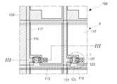
도 2와 도 3은 본 발명의 제 1 실시예에 따른 액정표시장치용 어레이기판의 일부 화소를 도시한 평면도와, 이를 Ⅲ-Ⅲ`을 따라 절단한 단면도이다.2 and 3 are a plan view showing some pixels of an array substrate for a liquid crystal display according to a first embodiment of the present invention, and sectional views thereof taken along line III-III '.
도시한 바와 같이, 기판(100)에 게이트배선(113)과 데이터배선(115)이 각각 매트릭스형태(matrix)로 교차하여 형성하고, 상기 게이트배선(113)과 데이터배선(115)의 교차지점에는 박막트랜지스터(T)를 형성한다. 상기 박막트랜지 스터(T)는 게이트전극(125), 액티브층(119), 소스전극(121), 드레인 전극(123)으로 구성한다.As shown in the drawing, a
상기 게이트배선(113)과 데이터배선(115)이 교차되어 정의되는 면적의 전면에는 화소전극(117)을 형성하고, 화소전극(117)은 콘택홀(127)을 통해 상기 드레인 전극(123)과 접촉하도록 한다.A
이와 같은 구성에서, 저 저항 불투명 절연막을 이용하여, 상기 게이트 배선(113)과 데이터 배선(115)과 박막트랜지스터(T)의 상부에, 상기 각 배선(113,115)과 화소 전극(117) 사이의 영역(K)까지 연장하여 블랙매트릭스 (저저항 절연막,134)을 형성한다.In this structure, a region between the
따라서, 빛샘 현상이 발생하는 영역인 각 배선(113, 115)과 화소전극(117)사이의 영역을 상기 블랙매트릭스(126)로 이미 차단하는 구조이기 때문에, 통상 합착 마진을 포함하여 패턴되는 블랙매트릭스를 형성한 종래의 액정표시장치에 비해 개구율을 더욱 확보할 수 있다.Therefore, since the region between the
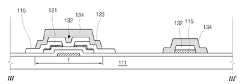
이하, 도 3a 내지 도 3c를 참조하여 전술한 바와 같은 어레이기판의 제작공정을 설명한다.Hereinafter, the fabrication process of the array substrate as described above with reference to Figs. 3A to 3C will be described.
도 3a 내지 도 3c는 도 2의 Ⅲ-Ⅲ`를 따라 절단하여 공정순서에 따라 도시한 공정 단면도이다.Figs. 3A to 3C are cross-sectional views of the process according to the order of cutting along III-III 'of Fig.
먼저, 도 3a에 도시한 바와 같이, 기판(100)상에 제 1 금속층을 형성하고 패턴하여, 게이트배선( 도 2의 113)과 게이트전극(125)을 형성한다. 이때, 상기 제 1 금속층은 알루미늄(Al), 알루미늄합금, 구리(Cu), 텅스텐(W), 몰리브덴(Mo), 크롬(Cr)으로 구성된 도전성 금속 그룹 중 하나를 선택하여 형성한다.First, as shown in Fig. 3A, a first metal layer is formed and patterned on a
다음으로, 상기 게이트전극(125)이 구성된 기판(100)의 전면에 질화 실리콘(SiNx) 또는 산화 실리콘(SiO2)을 증착하여 게이트 절연막(130)을 형성한다.Next, a gate
다음으로, 상기 게이트 전극(125)상부의 게이트 절연막(130)상에 순수 비정질 실리콘(a-Si:H)으로 형성한 액티브층(119)과 불순물 비정질 실리콘(n+ a-Si:H)으로 형성한 오믹콘택층(120)을 형성한다.Next, an
다음으로, 도 3b에 도시한 바와 같이, 상기 오믹콘택층(120)이 형성된 기판(100)의 전면에 제 2 금속층을 형성하고 패턴하여, 상기 게이트배선(113)과 교차하는 데이터배선(115)을 형성하고, 상기 데이터배선(115)에서 연장된 소스전극(121)과, 이와는 소정간격 이격된 드레인전극(123)을 형성한다.3B, a second metal layer is formed on the entire surface of the
다음으로, 상기 소스 및 드레인 전극(121,123)이 형성된 기판(100)의 전면에 전술한 무기절연 물질 중 선택된 하나를 증착하여 제 1 보호층(132)을 형성한다.Next, a selected one of the above-mentioned inorganic insulating materials is deposited on the entire surface of the
상기 제 1 보호층(132)은 하부의 액티브층(119)과 이후 공정에서 형성될 저저항 절연막이 접촉하는 것을 방지하는 역할을 한다.The
만약, 상기 액티브층(119)상에 제 1 보호층(132)이 존재하지 않는다면, 저저항 절연막과 접촉하는 액티브(119)층에 인가되는 문턱전압(Vth)의 값이 달라지므로, 게이트전극(125)에 전압을 인가하였을 경우, 상기 액티브층(119)의 표면에 전류가 흐르지 않거나 과도하게 흐르는 불량을 유발할 수 있다.If the first
다음으로, 상기 제 1 보호층(132)이 형성된 기판(100)의 전면에 컬러수지, 유기블랙매트릭스(블랙수지), 아크릴(Acryl)계 수지로 구성된 저저항 절연물질 그룹 중 선택된 하나를 도포하여 저저항 절연막(134)을 형성하고 패턴하여, 상기 데이터배선(115)과 박막트랜지스터(T)의 상부에 형성한다.Next, a selected one of a group of low-resistance insulating materials made of a color resin, an organic black matrix (black resin), and an acrylic resin is applied to the entire surface of the
이때, 상기 컬러필터 수지를 사용할 경우에는 상부기판(미도시)에 컬러필터를 구성하지 않는 대신 화소영역에 컬러필터 수지를 형성할 수도 있다.At this time, when the color filter resin is used, a color filter resin may be formed in a pixel region instead of forming a color filter on an upper substrate (not shown).
다음으로, 도 3c에 도시한 바와 같이, 상기 저저항 절연막(134)이 형성된 기판(100)의 상부에 전술한 바와 같은 유기 절연물질을 도포하여, 제 2 보호층(136)을 형성한다,Next, as shown in FIG. 3C, the organic insulating material as described above is applied to the upper portion of the
상기 제 2 보호층(136)은 아크릴(Acryl)계 수지와 벤조사이클로부텐(BCB)과 사이클로 올레핀(Cyclo-olefine)계열의 수지와 같은 유기절연막을 두텁게 증착하여 형성한다.The
다음으로, 상기 제 1 보호층(132)과 제 2 보호층(136)을 패턴하여, 상기 드레인 전극(123)의 일부를 노출하는 콘택홀(127)을 형성한다.Next, the
다음으로, 상기 패턴된 제 2 보호층(136)의 상부에 투명 도전성금속을 증착하고 패턴하여, 상기 드레인 전극(123)과 접촉하는 화소전극(117)을 형성한다.Next, a transparent conductive metal is deposited on the patterned
전술한 바와 같은 공정으로 본 발명에 따른 블랙매트릭스가 형성된 어레이기판을 제작할 수 있다.The array substrate on which the black matrix according to the present invention is formed can be manufactured by the process as described above.
전술한 바와 같은 구조는, 상부기판에 합착마진을 더한 별도의 블랙매트릭스를 구성할 필요가 없으므로, 액정패널의 개구율을 확보할 수 있는 구조이다.The structure as described above is a structure capable of securing the aperture ratio of the liquid crystal panel because there is no need to constitute a separate black matrix by adding the adhesion margin to the upper substrate.
그러나, 상기 저저항 절연막(134)과 하부 금속배선 사이에 기생용량이 발생 할 수 있으며, 이는 화질을 저하하는 원인이 될 수 있다.However, parasitic capacitance may be generated between the low
따라서, 전술한 제 1 예를 좀더 개선한 저저항막의 구조를 이하, 제 2 실시예에서 상세히 설명한다.
Therefore, the structure of the low resistance film which further improves the first example described above will be described in detail in the second embodiment.
- 실시예 2 -- Example 2 -
본 발명의 제 2 실시예에는 상기 저저항 절연막을 하부기판에 구성하되 상기 저저항 절연막과 하부 금속배선을 전기적으로 연결하여 등전위를 형성하는 구조를 제안한다.The second embodiment of the present invention proposes a structure in which the low resistance insulating film is formed on the lower substrate, and the low resistance insulating film and the lower metal wiring are electrically connected to form an equal potential.
이하, 도 4a 내지 도 4c를 참조하여, 본 발명의 제 2 실시예에 따른 어레이기판 제조공정을 설명한다.Hereinafter, an array substrate manufacturing process according to a second embodiment of the present invention will be described with reference to Figs. 4A to 4C.
도 4a 내지 도 4c는 도 2의 Ⅲ-Ⅲ`를 따라 절단하여 공정순서에 따라 도시한 공정 단면도이다.(제 1 실시예의 평면도와 동일하므로 도 2를 참조한다.)4A to 4C are cross-sectional views showing the process in accordance with the process sequence cut along III-III 'of FIG. 2. (See FIG. 2, which is the same as the plan view of the first embodiment.)
먼저, 도 4a에 도시한 바와 같이, 기판(100)상에 제 1 금속층을 형성하고 패턴하여, 게이트배선(도 2의 113)과 게이트전극(125)을 형성한다. 이때, 상기 제 1 금속층은 알루미늄(Al), 알루미늄합금, 구리(Cu), 텅스텐(W), 몰리브덴(Mo), 크롬(Cr)으로 구성된 도전성 금속 그룹 중 하나를 선택하여 형성한다.First, as shown in FIG. 4A, a first metal layer is formed on the
다음으로, 상기 게이트배선(113)이 구성된 기판(100)의 전면에 질화 실리콘(SiNx) 또는 산화 실리콘(SiO2)을 증착하여 게이트 절연막(130)을 형성한다.Next, a
다음으로, 상기 게이트 전극(125)상부의 게이트 절연막(130)상에 순수 비정 질 실리콘(a-Si:H)으로 형성한 액티브층(119)과 불순물 비정질 실리콘(n+ a-Si:H)으로 형성한 오믹콘택층(120)을 형성한다.Next, an
다음으로, 도 4b에 도시한 바와 같이, 상기 오믹콘택층(120)이 형성된 기판(100)의 전면에 제 2 금속층을 형성하고 패턴하여, 상기 게이트배선(도2의 113)과 교차하는 데이터배선(115)을 형성하고, 상기 데이터배선(115)에서 연장된 소스전극(121)과, 이와는 소정간격 이격된 드레인전극(123)을 형성한다.Next, as shown in FIG. 4B, a second metal layer is formed on the entire surface of the
다음으로, 상기 소스 및 드레인 전극(121,123)이 형성된 기판(100)의 전면에 전술한 무기절연 물질 중 선택된 하나를 증착하고 패턴하여, 상기 데이터배선(115)과 박막트랜지스터(T) 상부에만 제 1 보호층(132)을 형성한다.Next, a selected one of the above-mentioned inorganic insulating materials is deposited and patterned on the entire surface of the
즉, 제 2 보호층(136) 하부의 소스 및 드레인 전극(121, 123)의 일부(K1)를 노출하고, 상기 데이터배선의 측면(K2)을 노출한다.The portion K1 of the source and drain
다음으로, 상기 제 1 보호층(132)이 형성된 기판(100)의 전면에 컬러수지, 유기 블랙매트릭스, 아크릴계 수지로 구성된 저저항 절연물질 그룹 중 선택된 하나를 도포하여 저저항 절연막(134)을 형성한다.Next, a selected one of a group of low resistance insulating materials made of a color resin, an organic black matrix, and an acrylic resin is coated on the entire surface of the
이때, 상기 저저항 절연막(134)은, 상기 데이터배선(115)과 박막트랜지스터(T)의 상부에 구성하되, 상기 패턴된 제 1 보호층(132) 사이로 노출된 데이터배선(100)과 박막트랜지스터(T)의 금속전극에 접촉하여 구성한다.The low
상기 컬러필터 수지를 저저항 절연막으로 사용할 경우에는 상부기판에 컬러필터를 구성하지 않는 대신 화소영역 전체에 컬러필터 수지를 형성할 수도 있다.When the color filter resin is used as a low-resistance insulating film, a color filter resin may be formed on the entire pixel region instead of forming a color filter on the upper substrate.
이때, 상기 데이터 배선(115)에서는, 상기 저저항 절연막(134)이 상기 데이터배선(115) 상부에 패턴된 제 1 보호층(132)을 포함하여 상기 데이터배선(115)을 감싸는 구조로 형성한다.In this case, in the
이와 같이 하면 상기 저저항 절연막(134)과 하부의 금속배선이 접촉하여 등전위를 형성하는 구조가 되기 때문에, 상기 저저항 절연막(134)에 의해 발생할 수 있는 기생용량을 원천적으로 제거하는 구조임으로 화질이 저하되는 불량을 방지할 수 있다.In this case, since the low
다음으로, 도 4c에 도시한 바와 같이, 상기 저저항 절연막(134)이 형성된 기판(100)의 상부에 전술한 바와 같은 절연물질을 도포하여 제 2 보호층(136)을 형성한다,Next, as shown in FIG. 4C, a second
상기 제 2 보호층(136)은 아크릴(Acryl)계 수지(resin)와 벤조사이클로부텐(BCB)과 사이클로 올레핀(Cyclo olefine) 계열의 수지와 같은 유기절연막을 두텁게 증착하여 형성한다.The
다음으로, 상기 제 1 보호층(132)과 제 2 보호층(136)을 패턴하여, 상기 드레인 전극(125)의 일부를 노출하는 콘택홀(127)을 형성한다.Next, the
다음으로, 상기 패턴된 제 2 보호층(136)의 상부에 투명 도전성금속을 증착하고 패턴하여, 상기 드레인 전극(123)과 접촉하는 화소전극(117)을 형성한다.Next, a transparent conductive metal is deposited on the patterned
전술한 바와 같은 공정으로 본 발명의 제 2 실시예에 따른 어레이기판을 제작할 수 있다.
The array substrate according to the second embodiment of the present invention can be manufactured by the process as described above.
따라서, 전술한 바와 같은 본 발명에 따른 블랙매트릭스 형성방법은 아래와 같은 효과가 있다.Therefore, the method of forming a black matrix according to the present invention as described above has the following effects.
첫째, 저저항 절연막인 블랙매트릭스를 하부기판에 직접 형성하여, 합착마진을 고려할 필요가 없기 때문에 개구율을 개선하는 효과가 있다.First, since the black matrix as the low resistance insulating film is directly formed on the lower substrate, there is no need to consider the cohesion margin, and thus the aperture ratio is improved.
둘째, 상기 저저항 절연막을 하부의 금속배선과 연결하여 구성하기 때문에 상기 저저항 절연막과 하부 배선사이에 기생용량이 발생하지 않는다.Secondly, since the low-resistance insulating film is formed by connecting to the lower metal wiring, no parasitic capacitance is generated between the low-resistance insulating film and the lower wiring.
따라서, 크로스토크와 플리커 현상을 방지할 수 있기 때문에 화질이 저하되지 않는 효과가 있다.
Therefore, the crosstalk and the flicker phenomenon can be prevented, and the image quality is not deteriorated.
Claims (10)
Translated fromKoreanPriority Applications (2)
| Application Number | Priority Date | Filing Date | Title |
|---|---|---|---|
| KR1020000083762AKR100746140B1 (en) | 2000-12-28 | 2000-12-28 | Array substrate for liquid crystal display device and manufacturing method thereof |
| US10/015,894US6570631B2 (en) | 2000-12-28 | 2001-12-17 | Black matrix in liquid crystal display and method of fabricating the same |
Applications Claiming Priority (1)
| Application Number | Priority Date | Filing Date | Title |
|---|---|---|---|
| KR1020000083762AKR100746140B1 (en) | 2000-12-28 | 2000-12-28 | Array substrate for liquid crystal display device and manufacturing method thereof |
Publications (2)
| Publication Number | Publication Date |
|---|---|
| KR20020054608A KR20020054608A (en) | 2002-07-08 |
| KR100746140B1true KR100746140B1 (en) | 2007-08-03 |
Family
ID=19703760
Family Applications (1)
| Application Number | Title | Priority Date | Filing Date |
|---|---|---|---|
| KR1020000083762AExpired - Fee RelatedKR100746140B1 (en) | 2000-12-28 | 2000-12-28 | Array substrate for liquid crystal display device and manufacturing method thereof |
Country Status (2)
| Country | Link |
|---|---|
| US (1) | US6570631B2 (en) |
| KR (1) | KR100746140B1 (en) |
Families Citing this family (23)
| Publication number | Priority date | Publication date | Assignee | Title |
|---|---|---|---|---|
| JP3705264B2 (en)* | 2001-12-18 | 2005-10-12 | セイコーエプソン株式会社 | Display device and electronic device |
| KR100491143B1 (en) | 2001-12-26 | 2005-05-24 | 삼성에스디아이 주식회사 | Flat Panel Display with Black Matrix and Method for fabricating the Same |
| JP2003202593A (en)* | 2002-01-04 | 2003-07-18 | Fujitsu Display Technologies Corp | Liquid crystal display device substrate, liquid crystal display device having the same, and method of manufacturing the same |
| TWI277788B (en)* | 2002-05-13 | 2007-04-01 | Au Optronics Corp | Active matrix substrate of liquid crystal display device and method fabricating the same |
| TWI300508B (en)* | 2003-01-13 | 2008-09-01 | Toppoly Optoelectronics Corp | Liquid crystal display |
| US7164456B2 (en)* | 2003-04-08 | 2007-01-16 | Lg.Philips Lcd Co., Ltd | Liquid crystal display device and method of fabricating the same wherein having particular reflective electrode |
| KR101002332B1 (en)* | 2003-12-30 | 2010-12-17 | 엘지디스플레이 주식회사 | LCD and its manufacturing method |
| TWI322917B (en)* | 2004-03-02 | 2010-04-01 | Innolux Display Corp | Active matrix type liquid crystal display |
| US20050253917A1 (en)* | 2004-05-13 | 2005-11-17 | Quanyuan Shang | Method for forming color filters in flat panel displays by inkjetting |
| US20050255253A1 (en)* | 2004-05-13 | 2005-11-17 | White John M | Apparatus and methods for curing ink on a substrate using an electron beam |
| US7612373B2 (en)* | 2004-06-30 | 2009-11-03 | Lg Display Co., Ltd. | Liquid crystal display device and method of manufacturing liquid crystal display device with color filter layer on thin film transistor |
| TWI284246B (en)* | 2004-08-13 | 2007-07-21 | Au Optronics Corp | Pixel structure of a liquid crystal display and fabricating method thereof and liquid crystal display panel |
| GB2418062A (en)* | 2004-09-03 | 2006-03-15 | Seiko Epson Corp | An organic Field-Effect Transistor with a charge transfer injection layer |
| US20060159843A1 (en)* | 2005-01-18 | 2006-07-20 | Applied Materials, Inc. | Method of substrate treatment for manufacturing of color filters by inkjet printing systems |
| JP4772395B2 (en)* | 2005-06-24 | 2011-09-14 | 三菱電機株式会社 | Electro-optic display device and manufacturing method thereof |
| US7544723B2 (en)* | 2005-07-15 | 2009-06-09 | Applied Materials, Inc. | Blue printing ink for color filter applications |
| US20070015847A1 (en)* | 2005-07-15 | 2007-01-18 | Applied Materials, Inc. | Red printing ink for color filter applications |
| US7460267B2 (en)* | 2005-07-15 | 2008-12-02 | Applied Materials, Inc. | Green printing ink for color filter applications |
| KR100855782B1 (en)* | 2007-01-29 | 2008-09-01 | 비오이 하이디스 테크놀로지 주식회사 | Fs mode liquid crystal display device and manufacturing method thereof |
| JP6063766B2 (en)* | 2013-02-20 | 2017-01-18 | 株式会社ジャパンディスプレイ | Semiconductor device |
| CN103487982A (en) | 2013-08-19 | 2014-01-01 | 京东方科技集团股份有限公司 | Display device, array substrate, pixel structure and manufacturing method |
| KR102255379B1 (en)* | 2014-08-12 | 2021-05-26 | 삼성디스플레이 주식회사 | Display device and method of manufacturing the same |
| TWI694289B (en)* | 2019-02-20 | 2020-05-21 | 友達光電股份有限公司 | Display device |
Citations (4)
| Publication number | Priority date | Publication date | Assignee | Title |
|---|---|---|---|---|
| JPH09113889A (en)* | 1995-10-20 | 1997-05-02 | Kyocera Corp | Liquid crystal display |
| KR19980017194A (en)* | 1996-08-30 | 1998-06-05 | 구자홍 | Method for manufacturing substrate of liquid crystal display device and structure of substrate manufactured by the method |
| KR19980026562A (en)* | 1996-10-10 | 1998-07-15 | 구자홍 | LCD and its manufacturing method |
| KR20000048021A (en)* | 1998-12-10 | 2000-07-25 | 카네코 히사시 | Liquid crystal display device and manufacturing method thereof |
Family Cites Families (1)
| Publication number | Priority date | Publication date | Assignee | Title |
|---|---|---|---|---|
| US6211928B1 (en)* | 1996-03-26 | 2001-04-03 | Lg Electronics Inc. | Liquid crystal display and method for manufacturing the same |
- 2000
- 2000-12-28KRKR1020000083762Apatent/KR100746140B1/ennot_activeExpired - Fee Related
- 2001
- 2001-12-17USUS10/015,894patent/US6570631B2/ennot_activeExpired - Lifetime
Patent Citations (4)
| Publication number | Priority date | Publication date | Assignee | Title |
|---|---|---|---|---|
| JPH09113889A (en)* | 1995-10-20 | 1997-05-02 | Kyocera Corp | Liquid crystal display |
| KR19980017194A (en)* | 1996-08-30 | 1998-06-05 | 구자홍 | Method for manufacturing substrate of liquid crystal display device and structure of substrate manufactured by the method |
| KR19980026562A (en)* | 1996-10-10 | 1998-07-15 | 구자홍 | LCD and its manufacturing method |
| KR20000048021A (en)* | 1998-12-10 | 2000-07-25 | 카네코 히사시 | Liquid crystal display device and manufacturing method thereof |
Also Published As
| Publication number | Publication date |
|---|---|
| KR20020054608A (en) | 2002-07-08 |
| US6570631B2 (en) | 2003-05-27 |
| US20020085140A1 (en) | 2002-07-04 |
Similar Documents
| Publication | Publication Date | Title |
|---|---|---|
| KR100746140B1 (en) | Array substrate for liquid crystal display device and manufacturing method thereof | |
| KR100726132B1 (en) | Array substrate for liquid crystal display device and manufacturing method | |
| KR100857133B1 (en) | Array substrate for liquid crystal display device and manufacturing method thereof | |
| KR101177720B1 (en) | LCD and Method of fabricating of the same | |
| KR100638525B1 (en) | Manufacturing Method of Array Board for Color Liquid Crystal Display | |
| KR100884541B1 (en) | LCD and its manufacturing method | |
| KR100380142B1 (en) | Transflective liquid crystal display device | |
| KR100938887B1 (en) | Array substrate for liquid crystal display device and manufacturing method | |
| US5742365A (en) | Liquid crystal display device and method for manufacturing the same in which a light shielding layer is over the gate electrode or a gate electrode is in a trench | |
| US6842199B2 (en) | Array substrate for liquid crystal display device and the fabrication method of the same | |
| US6734049B2 (en) | Array substrate for liquid crystal display device and the fabrication method of the same | |
| US7167218B1 (en) | Liquid crystal display and method of manufacture | |
| KR100488936B1 (en) | LCD | |
| KR100930918B1 (en) | Array substrate for liquid crystal display device and manufacturing method | |
| KR101005552B1 (en) | Liquid crystal display substrate and manufacturing method thereof | |
| KR101189147B1 (en) | LCD and Method of fabricating of the same | |
| KR100719265B1 (en) | Array substrate for liquid crystal display device and manufacturing method | |
| KR101405367B1 (en) | Liquid crystal display device and manufacturing method thereof | |
| JP3982730B2 (en) | Method for manufacturing thin film transistor array substrate | |
| KR101262091B1 (en) | LCD and Method of fabricating of the same | |
| KR100333272B1 (en) | Liquid crystal display and method for fabricating the same | |
| KR101198216B1 (en) | LCD and Method of fabricating of the same | |
| KR101190044B1 (en) | LCD and Method of fabricating of the same | |
| KR100333984B1 (en) | Liquid crystal display and manufacturing method thereof | |
| KR101244387B1 (en) | LCD and Method of fabricating of the same |
Legal Events
| Date | Code | Title | Description |
|---|---|---|---|
| PA0109 | Patent application | St.27 status event code:A-0-1-A10-A12-nap-PA0109 | |
| PN2301 | Change of applicant | St.27 status event code:A-3-3-R10-R13-asn-PN2301 St.27 status event code:A-3-3-R10-R11-asn-PN2301 | |
| PG1501 | Laying open of application | St.27 status event code:A-1-1-Q10-Q12-nap-PG1501 | |
| A201 | Request for examination | ||
| PA0201 | Request for examination | St.27 status event code:A-1-2-D10-D11-exm-PA0201 | |
| R17-X000 | Change to representative recorded | St.27 status event code:A-3-3-R10-R17-oth-X000 | |
| D13-X000 | Search requested | St.27 status event code:A-1-2-D10-D13-srh-X000 | |
| D14-X000 | Search report completed | St.27 status event code:A-1-2-D10-D14-srh-X000 | |
| E902 | Notification of reason for refusal | ||
| PE0902 | Notice of grounds for rejection | St.27 status event code:A-1-2-D10-D21-exm-PE0902 | |
| AMND | Amendment | ||
| E13-X000 | Pre-grant limitation requested | St.27 status event code:A-2-3-E10-E13-lim-X000 | |
| P11-X000 | Amendment of application requested | St.27 status event code:A-2-2-P10-P11-nap-X000 | |
| P13-X000 | Application amended | St.27 status event code:A-2-2-P10-P13-nap-X000 | |
| E601 | Decision to refuse application | ||
| PE0601 | Decision on rejection of patent | St.27 status event code:N-2-6-B10-B15-exm-PE0601 | |
| AMND | Amendment | ||
| J201 | Request for trial against refusal decision | ||
| P11-X000 | Amendment of application requested | St.27 status event code:A-2-2-P10-P11-nap-X000 | |
| P13-X000 | Application amended | St.27 status event code:A-2-2-P10-P13-nap-X000 | |
| PJ0201 | Trial against decision of rejection | St.27 status event code:A-3-3-V10-V11-apl-PJ0201 | |
| PB0901 | Examination by re-examination before a trial | St.27 status event code:A-6-3-E10-E12-rex-PB0901 | |
| B701 | Decision to grant | ||
| PB0701 | Decision of registration after re-examination before a trial | St.27 status event code:A-3-4-F10-F13-rex-PB0701 | |
| GRNT | Written decision to grant | ||
| PR0701 | Registration of establishment | St.27 status event code:A-2-4-F10-F11-exm-PR0701 | |
| PR1002 | Payment of registration fee | St.27 status event code:A-2-2-U10-U11-oth-PR1002 Fee payment year number:1 | |
| PG1601 | Publication of registration | St.27 status event code:A-4-4-Q10-Q13-nap-PG1601 | |
| G170 | Re-publication after modification of scope of protection [patent] | ||
| PG1701 | Publication of correction | St.27 status event code:A-5-5-P10-P19-oth-PG1701 Patent document republication publication date:20080417 Republication note text:Request for Correction Notice (Document Request) Gazette number:1007461400000 Gazette reference publication date:20070803 | |
| PN2301 | Change of applicant | St.27 status event code:A-5-5-R10-R13-asn-PN2301 St.27 status event code:A-5-5-R10-R11-asn-PN2301 | |
| PR1001 | Payment of annual fee | St.27 status event code:A-4-4-U10-U11-oth-PR1001 Fee payment year number:4 | |
| R18-X000 | Changes to party contact information recorded | St.27 status event code:A-5-5-R10-R18-oth-X000 | |
| PR1001 | Payment of annual fee | St.27 status event code:A-4-4-U10-U11-oth-PR1001 Fee payment year number:5 | |
| R18-X000 | Changes to party contact information recorded | St.27 status event code:A-5-5-R10-R18-oth-X000 | |
| R18-X000 | Changes to party contact information recorded | St.27 status event code:A-5-5-R10-R18-oth-X000 | |
| PR1001 | Payment of annual fee | St.27 status event code:A-4-4-U10-U11-oth-PR1001 Fee payment year number:6 | |
| FPAY | Annual fee payment | Payment date:20130619 Year of fee payment:7 | |
| PR1001 | Payment of annual fee | St.27 status event code:A-4-4-U10-U11-oth-PR1001 Fee payment year number:7 | |
| FPAY | Annual fee payment | Payment date:20140630 Year of fee payment:8 | |
| PR1001 | Payment of annual fee | St.27 status event code:A-4-4-U10-U11-oth-PR1001 Fee payment year number:8 | |
| FPAY | Annual fee payment | Payment date:20150629 Year of fee payment:9 | |
| PR1001 | Payment of annual fee | St.27 status event code:A-4-4-U10-U11-oth-PR1001 Fee payment year number:9 | |
| FPAY | Annual fee payment | Payment date:20160630 Year of fee payment:10 | |
| PR1001 | Payment of annual fee | St.27 status event code:A-4-4-U10-U11-oth-PR1001 Fee payment year number:10 | |
| PR1001 | Payment of annual fee | St.27 status event code:A-4-4-U10-U11-oth-PR1001 Fee payment year number:11 | |
| PR1001 | Payment of annual fee | St.27 status event code:A-4-4-U10-U11-oth-PR1001 Fee payment year number:12 | |
| PC1903 | Unpaid annual fee | St.27 status event code:A-4-4-U10-U13-oth-PC1903 Not in force date:20190731 Payment event data comment text:Termination Category : DEFAULT_OF_REGISTRATION_FEE | |
| PC1903 | Unpaid annual fee | St.27 status event code:N-4-6-H10-H13-oth-PC1903 Ip right cessation event data comment text:Termination Category : DEFAULT_OF_REGISTRATION_FEE Not in force date:20190731 |