KR100745496B1 - Laminated coil - Google Patents
Laminated coilDownload PDFInfo
- Publication number
- KR100745496B1 KR100745496B1KR1020067013182AKR20067013182AKR100745496B1KR 100745496 B1KR100745496 B1KR 100745496B1KR 1020067013182 AKR1020067013182 AKR 1020067013182AKR 20067013182 AKR20067013182 AKR 20067013182AKR 100745496 B1KR100745496 B1KR 100745496B1
- Authority
- KR
- South Korea
- Prior art keywords
- coil
- conductor
- laminated
- nonmagnetic
- magnetic
- Prior art date
- Legal status (The legal status is an assumption and is not a legal conclusion. Google has not performed a legal analysis and makes no representation as to the accuracy of the status listed.)
- Active
Links
Images


Classifications
- H—ELECTRICITY
- H01—ELECTRIC ELEMENTS
- H01F—MAGNETS; INDUCTANCES; TRANSFORMERS; SELECTION OF MATERIALS FOR THEIR MAGNETIC PROPERTIES
- H01F17/00—Fixed inductances of the signal type
- H01F17/0006—Printed inductances
- H01F17/0013—Printed inductances with stacked layers
- H—ELECTRICITY
- H01—ELECTRIC ELEMENTS
- H01F—MAGNETS; INDUCTANCES; TRANSFORMERS; SELECTION OF MATERIALS FOR THEIR MAGNETIC PROPERTIES
- H01F3/00—Cores, Yokes, or armatures
- H01F3/10—Composite arrangements of magnetic circuits
- H01F3/14—Constrictions; Gaps, e.g. air-gaps
- H—ELECTRICITY
- H01—ELECTRIC ELEMENTS
- H01F—MAGNETS; INDUCTANCES; TRANSFORMERS; SELECTION OF MATERIALS FOR THEIR MAGNETIC PROPERTIES
- H01F5/00—Coils
- H01F5/003—Printed circuit coils
Landscapes
- Engineering & Computer Science (AREA)
- Power Engineering (AREA)
- Microelectronics & Electronic Packaging (AREA)
- Chemical & Material Sciences (AREA)
- Composite Materials (AREA)
- Coils Or Transformers For Communication (AREA)
- Particle Accelerators (AREA)
- Coils Of Transformers For General Uses (AREA)
Abstract
Description
Translated fromKorean본 발명은 적층 코일 특히, 우수한 직류 중첩 특성을 가지는 개자로형(開磁路型) 적층 코일에 관한 것이다.BACKGROUND OF THE INVENTION Field of the Invention The present invention relates to laminated coils, and in particular to open-loop laminated coils having excellent direct current superimposition characteristics.
종래부터, 적층 코일에 있어서는 자성체내에서 자기 포화가 생겨 급격히 인덕턴스 값이 저하되어버리는 것을 방지하기 위해 개자로형 적층 코일이 제안되어 있다. 특허문헌(1)에 기재되어 있는 바와 같이, 개자로형 적층 코일은 자성체층에 의해 형성된 적층 코일의 내부에 비자성체층을 형성하고 있다. 개자로형 적층 코일의 구조에서는 비자성체층의 부분으로부터 자속이 적층 코일의 외부로 누설되어 자성체내에서 자기 포화가 생기기 어려워진다. 그 결과, 직류 전류에 의한 인덕턴스의 저하가 작아져서 직류 중첩 특성이 향상된다.Background Art Conventionally, in order to prevent magnetic saturation from occurring in a magnetic body and the inductance value drops rapidly in a laminated coil, an individual-type laminated coil has been proposed. As described in Patent Literature (1), an individual-type laminated coil forms a nonmagnetic layer inside a laminated coil formed of a magnetic layer. In the structure of the self-opening laminated coil, magnetic flux leaks from the portion of the nonmagnetic layer to the outside of the laminated coil, making it difficult to generate magnetic saturation in the magnetic body. As a result, the fall of inductance by DC current becomes small, and DC superimposition characteristic improves.
그러나, 특허문헌(1)의 개자로형 적층 코일에서는 직류 중첩 특성은 우수하지만, 인덕턴스 특성이 나쁘다는 문제가 있었다. 즉, 비자성체층은 자속이 통과하는 위치에 형성되어 있으므로 자속이 차단되어 인덕턴스가 작아져버리는 것이다. 소망의 인덕턴스를 취득하기 위해 코일의 권수를 증가시킴으로써 인덕턴스를 크게 하는 것이 고려되지만, 코일의 권수를 증가시키면 직류 저항이 대폭 커져버린다.However, in the open-air type laminated coil of patent document (1), although the DC superposition characteristic was excellent, there existed a problem that the inductance characteristic was bad. That is, since the nonmagnetic layer is formed at a position through which the magnetic flux passes, the magnetic flux is blocked and the inductance is reduced. It is considered to increase the inductance by increasing the number of turns of the coil in order to obtain a desired inductance, but increasing the number of turns of the coil greatly increases the DC resistance.
특허문헌1: 일본 특허 공개 평1-35483호Patent Document 1: Japanese Patent Application Laid-open No. Hei 1-35483
따라서, 본 발명의 목적은 우수한 직류 중첩 특성을 가지고, 인덕턴스의 저하를 억제하며, 또한 직류 저항을 감소시킨 적층 코일을 제공하는 것에 있다.It is therefore an object of the present invention to provide a laminated coil having excellent direct current superimposition characteristics, suppressing the reduction of inductance and reducing the direct current resistance.
상기 문제점을 해결하기 위해 본 발명에 의한 적층 코일은 (a) 복수의 자성체층을 적층한 자성체부가 1층 이상의 비자성체층으로 이루어지는 비자성체부의 양쪽 주면(主面)에 형성된 적층체와, (b) 상기 적층체에 형성된 코일 도체를 나선상으로 접속한 코일을 구비하고, (c) 상기 적층체에 형성된 코일 도체 중 상기 비자성체부의 내부에 형성된 코일 도체 및 상기 비자성체부의 양쪽 주면에 형성된 코일 도체의 1개 이상의 코일 도체의 도체폭이 다른 코일 도체의 도체폭 보다도 넓은 것을 특징으로 한다.In order to solve the above problems, the laminated coil according to the present invention comprises: (a) a laminated body formed on both main surfaces of a nonmagnetic material portion in which a magnetic body portion in which a plurality of magnetic body layers are laminated is formed of at least one nonmagnetic layer, and (b) A coil having spirally connected coil conductors formed in the laminate, and (c) a coil conductor formed inside the nonmagnetic portion of the coil conductors formed in the laminate and coil conductors formed on both main surfaces of the nonmagnetic portion. A conductor width of at least one coil conductor is wider than that of other coil conductors.
비자성체부의 내부 및 비자성체부의 양쪽 주면(主面)에 형성된 코일 도체의 1개 이상의 코일 도체의 도체폭을 다른 코일 도체의 도체폭 보다도 넓게 함으로써, 직류 저항을 감소시킬 수 있다. 또한, 도체폭이 넓은 코일 도체를 비자성체부의 내부 및/또는 양쪽 주면에 형성함으로써 코일 도체의 도체폭을 넓게 해도 인덕턴스의 저하를 작게 할 수 있다.DC resistance can be reduced by making the conductor width of one or more coil conductors of the coil conductors formed on both the inner surface of the nonmagnetic portion and the main surface of the nonmagnetic portion larger than that of the other coil conductors. In addition, by forming a coil conductor having a wide conductor width inside and / or on both main surfaces of the nonmagnetic portion, the reduction in inductance can be reduced even if the conductor width of the coil conductor is widened.
즉, 일반적으로 코일 도체의 도체폭을 넓게 하면 도체폭이 넓은 코일 도체에 코일의 자속이 차단되고, 또한 코일의 내경이 좁아져서 코일의 자속이 통과하는 양이 적어지기 때문에 인덕턴스가 저하된다. 그러나, 비자성체부의 코일 도체의 도체폭을 넓게 해도 원래 비자성체부에 의해 코일의 자속이 차단되어 있었으므로, 코일 도체의 도체폭을 넓게 함으로써 더욱 차단되는 코일의 자속은 매우 적어진다. 또한, 코일 도체의 도체폭을 넓게 해도 자속을 차단하는 비자성체부에 있어서의 코일의 내경이 작아지므로, 자속을 통과시키는 자성체부의 코일의 내경이 작아지는 것에 비해 자속이 통과하는 양의 감소는 작아진다. 따라서, 코일 전체의 인덕턴스의 저하를 작게 할 수 있는 것이다.That is, in general, when the conductor width of the coil conductor is widened, the magnetic flux of the coil is blocked by the coil conductor having a wider conductor width, and the inner diameter of the coil is narrowed, so that the amount of magnetic flux passing through the coil decreases, thereby reducing the inductance. However, even if the conductor width of the coil conductor of the nonmagnetic portion is widened, the magnetic flux of the coil was originally blocked by the nonmagnetic portion, so that the magnetic flux of the coil further blocked by increasing the conductor width of the coil conductor is very small. In addition, even if the conductor width of the coil conductor is widened, the inner diameter of the coil in the nonmagnetic portion that blocks the magnetic flux becomes small, so that the decrease in the amount of the magnetic flux passes is small compared to that of the coil of the magnetic portion that allows the magnetic flux to pass. Lose. Therefore, the fall of the inductance of the whole coil can be made small.
본 발명에 의한 적층 코일은 상기 비자성체부의 내부에 형성된 코일 도체 및 상기 비자성체부의 양쪽 주면에 형성된 코일 도체의 도체폭을 다른 코일 도체의 도체폭 보다도 넓게 해도 좋다. 비자성체부의 내부 및 비자성체부의 양쪽 주면에 형성된 코일 도체의 도체폭을 넓게 함으로써, 도체폭이 넓은 코일 도체가 복수 형성되어 직류 저항을 대폭 감소시킬 수 있다.In the laminated coil according to the present invention, the conductor width of the coil conductor formed inside the nonmagnetic portion and the coil conductor formed on both main surfaces of the nonmagnetic portion may be wider than the conductor width of the other coil conductor. By widening the conductor widths of the coil conductors formed on both the inner surface of the nonmagnetic portion and on both main surfaces of the nonmagnetic portion, a plurality of coil conductors having a wide conductor width can be formed, thereby greatly reducing the DC resistance.
또한, 본 발명에 의한 적층 코일은 상기 도체폭이 넓은 코일 도체의 도체폭이 다른 코일 도체의 도체폭의 1.05 ∼ 2.14배인 것이 바람직하다. 이에 따라, 인덕턴스의 저하를 극력 억제하고, 또한 직류 저항을 대폭 감소시킨 적층 코일을 얻을 수 있다.Moreover, it is preferable that the laminated coil by this invention is 1.05-2.14 times the conductor width of the coil conductor from which the conductor width of the said coil conductor with wide conductor width differs. Thereby, the laminated coil which suppressed the fall of an inductance as much as possible and greatly reduced the DC resistance can be obtained.
또한, 본 발명에 의한 적층 코일은 상기 적층체의 내부에 상기 비자성체부가 복수 형성되어 있어도 좋다. 비자성체부를 적층체의 내부에 복수 형성함으로써 비자성체부로부터 적층 코일의 외부로 누설되는 자속의 양을 더욱 증가시킬 수 있고, 직류 중첩 특성을 향상시킬 수 있다.In the multilayer coil according to the present invention, a plurality of nonmagnetic portions may be formed inside the laminate. By forming a plurality of nonmagnetic parts inside the laminate, the amount of magnetic flux leaking from the nonmagnetic parts to the outside of the laminated coil can be further increased, and the direct current superimposition characteristic can be improved.
이와 같이 본 발명에 의하면, 비자성체부의 내부에 형성된 코일 도체 및 비자성체부의 양쪽 주면에 형성된 코일 도체 중 1개 이상의 코일 도체의 도체폭이 다른 코일 도체의 도체폭 보다도 넓으므로 우수한 직류 중첩 특성을 가지며, 인덕턴스의 저하를 억제하고, 또한 직류 저항을 감소시킨 적층 코일을 얻을 수 있다.As described above, according to the present invention, since the conductor width of one or more coil conductors among the coil conductors formed inside the non-magnetic portion and the coil conductors formed on both main surfaces of the non-magnetic portion is wider than that of the other coil conductors, it has excellent DC superposition characteristics. The laminated coil which suppressed the fall of inductance and reduced DC resistance can be obtained.
도 1은 본 발명의 실시예 1에 있어서의 적층 코일의 개략 단면도이다.BRIEF DESCRIPTION OF THE DRAWINGS It is a schematic sectional drawing of the laminated coil in Example 1 of this invention.
도 2는 본 발명의 실시예 1에 있어서의 적층 코일의 분해 사시도이다.Fig. 2 is an exploded perspective view of the laminated coil in the first embodiment of the present invention.
도 3은 종래예의 적층 코일의 개략 단면도이다.3 is a schematic cross-sectional view of a laminated coil of a conventional example.
도 4는 비교예 1의 적층 코일의 개략 단면도이다.4 is a schematic cross-sectional view of a laminated coil of Comparative Example 1. FIG.
도 5는 본 발명의 실시예 3에 있어서의 적층 코일의 개략 단면도이다.5 is a schematic cross-sectional view of a laminated coil in a third embodiment of the present invention.
도 6은 본 발명의 실시예 4에 있어서의 적층 코일의 개략 단면도이다.6 is a schematic cross-sectional view of a laminated coil in a fourth embodiment of the present invention.
도 7은 본 발명의 실시예 5에 있어서의 적층 코일의 개략 단면도이다.7 is a schematic cross-sectional view of a laminated coil in a fifth embodiment of the present invention.
도 8은 비교예 2의 적층 코일의 개략 단면도이다.8 is a schematic cross-sectional view of a laminated coil of Comparative Example 2. FIG.
이하, 본 발명에 의한 적층 코일의 실시예를 도면을 참조해서 설명한다.EMBODIMENT OF THE INVENTION Hereinafter, the Example of the laminated coil by this invention is described with reference to drawings.
(실시예 1)(Example 1)
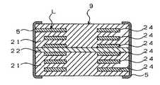
도 1은 본 발명의 실시예 1에 있어서의 적층 코일의 개략 단면도이다. 적층 코일은 자성체부(1) 및 비자성체부(2)로 이루어지는 적층체(9)와, 적층체(9)에 형성된 코일 도체(3, 4)를 나선상으로 접속한 코일(L)과, 외부 전극(5)으로 형성되어 있다. 자성체부(1)는 비자성체부(2)의 양쪽 주면에 형성되어 있다. 또한, 자성체부(1)는 복수의 자성체층으로 구성되어 있고, 비자성체부(2)는 1층의 비자성체층으로 구성되어 있다.BRIEF DESCRIPTION OF THE DRAWINGS It is a schematic sectional drawing of the laminated coil in Example 1 of this invention. The laminated coil includes a laminated
도 1에 도시한 바와 같이, 코일 도체(4)는 비자성체부(2)의 양쪽 주면에 형 성되어 있고, 다른 소정의 도체폭을 가지는 코일 도체(3) 보다도 도체폭이 넓게 되어있다. 코일 도체(4)의 도체폭이 넓기 때문에 적층 코일의 직류 저항은 저하된다.As shown in Fig. 1, the
또한, 도체폭이 넓은 코일 도체(4)가 비자성체부(2)의 양쪽 주면에 형성되어 있으므로 인덕턴스의 저하를 작게 할 수 있다. 즉, 일반적으로 코일 도체의 도체폭을 넓게 하면 도체폭이 넓은 코일 도체에 코일의 자속이 차단되고, 또한 코일의 내경이 좁아져서 코일의 자속이 통과하는 양이 적어지기 때문에 인덕턴스가 저하된다. 그러나, 실시예 1과 같이 비자성체부(2)의 양쪽 주면의 코일 도체(4)의 도체폭을 넓게 하더라도 원래 비자성체부(2)에 의해 코일(L)의 자속이 차단되어 있었으므로, 코일 도체(4)의 도체폭을 넓게 함으로써 더욱 차단되는 코일(L)의 자속은 매우 적어진다. 또한, 코일 도체(4)의 도체폭을 넓게 하더라도 자속을 차단하는 비자성체부(2)에 있어서의 코일(L)의 내경이 작아지므로, 자속을 통과시키는 자성체부(1)의 코일(L)의 내경이 작아지는 것에 비해 자속이 통과하는 양의 감소는 작아진다. 따라서, 코일(L) 전체의 인덕턴스의 저하를 매우 작게 할 수 있는 것이다.Moreover, since the
이어서, 적층 코일의 제조 방법에 대해서 도 2에 도시한 적층 코일의 분해 사시도를 이용해서 설명한다.Next, the manufacturing method of a laminated coil is demonstrated using the exploded perspective view of the laminated coil shown in FIG.
적층 코일의 제조 방법에 있어서는, 처음에 자성체 재료를 사용한 그린 시트(green sheet)(6) 및 비자성체 재료를 사용한 그린 시트(7)를 제작한다. 또한, 적층 코일 형성 후에는 자성체 그린 시트가 자성체층, 비자성체 그린 시트가 비자성체층이 된다.In the manufacturing method of a laminated coil, the
본 실시예 1에서는 자성체 재료로서 Ni-Cu-Zn계 재료를 사용했다. 우선, 산 화 제2철(Fe2O3) 48.0mol%, 산화 아연(ZnO) 20.0mol%, 산화 니켈(NiO) 23.0mol%, 산화 구리(CuO) 9.0mol%의 비율의 재료를 원료로 하여 볼 밀(ball mill)을 이용해서 습식 조합을 행한다. 얻어진 혼합물을 건조한 후 분쇄하고, 그 분말을 750℃에서 1시간 가소(假燒)한다. 이 분말에 바인더 수지와 가소제, 습윤제, 분산제를 첨가해서 볼 밀에 의해 혼합을 행하고, 그 후 탈포(脫泡)를 행하여 슬러리를 얻는다. 그리고, 이 슬러리를 박리성의 필름 상에 도포하고, 건조시킴으로써 소망의 막 두께의 자성체 그린 시트(6)를 제작한다.In Example 1, a Ni—Cu—Zn-based material was used as the magnetic material. First, the material was composed of 48.0 mol% of ferric oxide (Fe2 O3 ), 20.0 mol% of zinc oxide (ZnO), 23.0 mol% of nickel oxide (NiO), and 9.0 mol% of copper oxide (CuO). Wet combination is performed using a ball mill. The obtained mixture is dried and then ground, and the powder is calcined at 750 ° C. for 1 hour. Binder resin, a plasticizer, a wetting agent, and a dispersing agent are added to this powder, it mixes by a ball mill, and it defoases after that, and obtains a slurry. And this slurry is apply | coated on a peelable film and dried, and the magnetic
또한, 비자성체 재료로서 Cu-Zn계 재료를 사용했다. 산화 제2철(Fe2O3) 48.0mol%, 산화 아연(ZnO) 43.0mol%, 산화 구리(CuO) 9.0mol%의 비율을 원료로 해서 상기 자성체와 마찬가지의 방법에 의해 비자성체 그린 시트(7)를 제작한다. 한편, 각 그린 시트의 비 투자율은 자성체 그린 시트(6)가 130, 비자성체 그린 시트(7)가 1이다.Moreover, Cu-Zn type material was used as a nonmagnetic material. A nonmagnetic green sheet was prepared by the same method as the above magnetic material using a ratio of 48.0 mol% of ferric oxide (Fe2 O3 ), 43.0 mol% of zinc oxide (ZnO), and 9.0 mol% of copper oxide (CuO). 7) to produce. On the other hand, the specific magnetic permeability of each green sheet is 130 for the magnetic
이어서, 이상과 같이 해서 얻어진 각 그린 시트(6, 7)를 소정의 치수로 재단하고, 각 그린 시트(6, 7)의 적층 후에 나선상의 코일(L)이 형성되도록, 소정의 위치에 레이저 등의 방법에 의해 관통 구멍을 형성한다. 그리고, 자성체 그린 시트(6a) 및 비자성체 그린 시트(7) 상에 은 또는 은합금을 주성분으로 하는 도체 페이스트를 스크린 인쇄 등의 방법에 의해 도포함으로써 코일 도체(3, 4)를 형성한다. 한편, 코일 도체(3, 4)의 형성과 동시에 관통 구멍의 내부에 도전 페이스트를 충전함으로써 용이하게 접속용 비어 홀 도체(8)를 형성할 수 있다.Subsequently, each
여기에서, 비자성체 그린 시트(7)의 양쪽 주면에 위치하도록 폭이 넓은 코일 도체(4)를 형성한다. 본 실시예 1에서는 폭이 넓은 코일 도체(4)는 소성 후에 550㎛, 기타 코일 도체(3)의 도체폭은 350㎛가 되도록 형성했다. 폭이 넓은 코일 도체(4)를 비자성체 그린 시트(7)의 양쪽 주면에 형성함으로써 인덕턴스의 저하를 억제하고, 또한 직류 저항이 감소된 적층 코일을 얻을 수 있다.Here, the
그리고, 비자성체 그린 시트(7)의 양쪽 주면에 코일 도체(3)를 형성한 자성체 그린 시트(6a)를 적층하고, 상하에 코일 도체를 형성하고 있지 않은 외층용 자성체 그린 시트(6b)를 배치함으로써 적층체를 형성한다. 이 때, 비자성체 그린 시트(7)가 나선상의 코일(L)의 축심 방향의 대략 중앙에 위치하도록 적층함으로써 적층 코일의 외부로 누설되는 자속이 많아져 직류 중첩 특성을 향상시킬 수 있다.And the magnetic green sheet 6a which formed the
그 후, 적층체를 45℃, 1.Ot/㎠의 압력으로 압착하고, 다이서(dicer)나 길로틴 커터(guillotine cutter)에 의해 3.2×2.5×0.8mm의 치수로 재단함으로써 적층 코일의 미소성체를 얻는다. 그리고, 이 미소성체의 탈(脫)바인더 및 본소성(本燒成)을 행한다. 탈 바인더는 저 산소 분위기 중에 있어서 500℃에서 2시간 가열하고, 본 소성은 대기 분위기 중에 있어서 890℃에서 150분으로 소성한다. 최후에, 인출 전극이 노출되는 단부면에 침지법 등에 의해 주성분이 은인 전극 페이스트를 도포하고, 100℃에서 10분 건조한 후, 780℃에서 150분간을 베이킹(baking)한다. 이에 따라, 실시예 1의 적층 코일을 얻을 수 있다.Thereafter, the laminated body was pressed at 45 ° C. at a pressure of 1.Ot /
표 1는 상기에 의해 얻어진 실시예 1의 적층 코일의 효과를 확인하기 위해 행한 시험 결과를 나타낸다. 종래예는 도 3에 도시한 바와 같이, 자성체부(11) 및 비자성체부(12)에 형성된 코일 도체(13)의 도체폭이 모두 350㎛인 적층 코일이다. 또한, 비교예는 도 4에 도시한 바와 같이 자성체부(21) 및 비자성체부(22)에 형성된 코일 도체(24)의 도체폭이 모두 넓으며, 550㎛인 적층 코일이다. 또한, 모든 적층 코일에 있어서, 나선상 코일(L)의 권회수는 5.5턴(turn)이며, 적층 코일의 사이즈는 3.2mm×2.5mm×2.5mm이다.Table 1 shows the test results performed to confirm the effect of the laminated coil of Example 1 obtained above. As shown in Fig. 3, the conventional coil is a laminated coil in which the conductor widths of the
표 1로부터, 실시예 1의 적층 코일은 직류 저항이 감소하고, 인덕턴스의 저하가 작다는 것을 알 수 있다. 즉, 종래예의 직류 저항은 185mΩ인 것에 대해, 실시예 1의 직류 저항은 166mΩ이며, 직류 저항이 10% 감소되어 있다. 한편, 종래예의 인덕턴스는 2.0μH인 것에 대해, 실시예 1의 인덕턴스는 1.91μH이며, 4.5% 밖에 감소되어 있지 않다. 이것에 대해, 모든 코일 도체의 도체폭을 넓게 한 비교예에서는 직류 저항이 150mΩ과 18%감소되어 있지만, 인덕턴스가 1.56μH이며 저하가 22%로 크다. 이와 같이, 실시예 1에 있어서 코일 도체(4)의 도체폭을 넓게 해서 직류 저항을 감소시키면서도, 코일 도체(4)의 도체폭을 넓게 함에 의한 인덕턴스의 저하를 억제할 수 있었던 것은 도체폭이 넓은 코일 도체(4)를 자속을 차단하는 비자성체부(2)의 양쪽 주면에 형성한 것에 의한다.It can be seen from Table 1 that the laminated coil of Example 1 has a reduced DC resistance and a small decrease in inductance. That is, while the DC resistance of the conventional example is 185 mΩ, the DC resistance of Example 1 is 166 mΩ, and the DC resistance is reduced by 10%. On the other hand, while the inductance of the conventional example is 2.0 µH, the inductance of Example 1 is 1.91 µH, which is reduced by only 4.5%. On the other hand, in the comparative example in which the conductor widths of all the coil conductors were widened, the DC resistance was reduced by 150 m? And 18%. However, the inductance was 1.56 µH and the decrease was as large as 22%. As described above, in Example 1, the conductor width of the
이어서, 표 2에서는 비자성체부(2)의 양쪽 주면에 형성한 코일 도체(4)의 도체폭을 변화시킨 시료 1∼7의 평가 결과를 나타낸다. 시료 1∼7에서는 비자성체부(2)의 양쪽 주면에 형성된 코일 도체(4)의 도체폭을 357, 368, 450, 550, 650, 750, 850㎛로 다르게 해서 시작(試作)했다. 한편, 종래예는 도 3에 도시된 도체폭이 모두 동일한 350㎛인 적층 코일이다.Next, Table 2 shows the evaluation results of
시료 2∼6에서는 직류 저항이 감소하고, 인덕턴스 값도 바람직하다. 한편, 시료1(도체폭 비 1.02)에서는 직류 저항의 저하율이 1%미만으로 대단히 작았다. 또한, 시료7(도체폭 비 2.43)에서는 종래예와 비교한 인덕턴스 값의 감소율이 14.5%로 크게 감소되어버렸다.In
(실시예 2)(Example 2)
본 발명의 실시예 2에 있어서의 적층 코일의 구성은 도 1에 도시된 실시예 1에 있어서의 적층 코일의 구성과 같지만, 본 실시예 2에 있어서는 비자성체부(2)의 양쪽 주면에 위치하는 코일 도체(4)의 도체폭을 750㎛로 하고, 비자성체부(2)의 양쪽 주면에 위치하고 있지 않은 코일 도체(3)의 도체폭(3)을 350㎛로 했다. 한편, 이하의 표 3에서 나타내는 종래예는 도 3에 도시한 바와 같이 자성체부(11) 및 비자성체부(12)에 형성된 코일 도체(13)의 도체폭이 모두 350㎛인 적층 코일이다. 또한, 비교예 2는 도 8에 도시한 바와 같이 비자성체부(32)의 양쪽 주면에 형성되어 있지 않은[자성체부(31)의 내부에 형성된] 코일 도체(34)의 도체폭이 다른 코일 도체(33) 보다도 넓은 적층 코일이며, 도체폭이 넓은 코일 도체(34)의 도체폭은 750㎛이고, 다른 코일 도체(33)의 도체폭은 350㎛이다.Although the structure of the laminated coil in Example 2 of this invention is the same as the structure of the laminated coil in Example 1 shown in FIG. 1, in this Example 2, it is located in the both main surfaces of the
표(3)에 나타낸 바와 같이, 실시예 2의 적층 코일은 비자성체부(2)의 양쪽 주면에 위치하는 코일 도체(4)의 도체폭을 넓게 하고 있으므로, 종래예와 비교해서 직류 저항이 감소되어 있다. 그리고, 비교예 2의 적층 코일에 있어서도 실시예 2의 적층 코일과 동일한 턴 수 만큼의 코일 도체(34)의 도체폭을 넓게 하고 있으므로, 종래예와 비교해서 직류 저항이 저하되어 있다. 그러나, 실시예 2의 적층 코일의 인덕턴스는 1.79μH이며, 종래예와 비교해서 10% 정도 밖에 감소되어 있지 않는 것에 대해, 비교예 2의 적층 코일의 인덕턴스는 1.53μH이며, 종래예와 비교해서 23% 정도 감소되어 있다. 이와 같이, 실시예 2의 적층 코일이 인덕턴스의 저하를 억제할 수 있었던 것은 도체폭이 넓은 코일 도체(4)를 자속을 차단하는 비자성체부(2)의 양쪽 주면에 형성한 것에 의한다.As shown in Table (3), the laminated coil of Example 2 widens the conductor width of the
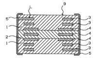
(실시예 3)(Example 3)
도 5에서 본 발명의 실시예 3에 있어서의 적층 코일의 개략 단면도를 도시한다. 한편, 도 5에 있어서는 도 1과 공통 또는 대응되는 부분에는 동일한 부호를 붙이고, 적당히 설명을 생략한다.In FIG. 5, schematic sectional drawing of the laminated coil in Example 3 of this invention is shown. 5, the same code | symbol is attached | subjected to the part common or corresponding to FIG. 1, and description is abbreviate | omitted suitably.
본 실시예 3의 적층 코일에 있어서, 코일 도체(4)는 비자성체부(2)의 내부에 형성되어 있고, 코일 도체(4)의 도체폭은 다른 코일 도체(3)의 도체폭 보다도 넓다. 또한, 본 실시예 3의 적층 코일도 실시예 1과 마찬가지로, 코일 도체를 형성한 그린 시트를 적층, 압착하고, 각 칩으로 재단한 후, 외부 전극을 형성하는 방법에 의해 제작하고 있다.In the laminated coil of the third embodiment, the
도체폭이 넓은 코일 도체(4)를 형성함으로써 직류 저항을 저감할 수 있다. 또한, 도체폭이 넓은 코일 도체(4)를 비자성체부(2)의 내부에 형성함으로써 인덕턴스의 저하를 작게 할 수 있다.The DC resistance can be reduced by forming the
(실시예 4)(Example 4)
도 6에서 본 발명의 실시예 4에 있어서의 적층 코일의 개략 단면도를 도시한다. 한편, 도 6에 있어서는 도 1과 공통 또는 대응되는 부분에는 동일한 부호를 붙이고, 그 설명을 생략한다.In FIG. 6, schematic sectional drawing of the laminated coil in Example 4 of this invention is shown. 6, the same code | symbol is attached | subjected to the part common or corresponding to FIG. 1, and the description is abbreviate | omitted.
본 실시예 4의 적층 코일에 있어서, 코일 도체(4)는 비자성체부(2)의 내부 및 비자성체부(2)의 양쪽 주면에 형성되어 있고, 코일 도체(4)의 도체폭은 다른 코일 도체(3)의 도체폭 보다도 넓다.In the laminated coil of the fourth embodiment, the
도체폭이 넓은 코일 도체(4)를 형성함으로써 직류 저항을 저감할 수 있다. 특히, 본 실시예 4에서는 도체폭이 넓은 코일 도체(4)를 3층에 걸쳐 형성하고 있으므로, 대폭 직류 저항을 저감할 수 있다. 또한, 도체폭이 넓은 코일 도체(4)를 비자성체부(2)의 내부 및 비자성체부(2)의 양쪽 주면에 형성함으로써 인덕턴스의 저하를 작게 할 수 있다.The DC resistance can be reduced by forming the
(실시예 5)(Example 5)
도 7에 본 발명의 실시예 5에 있어서의 적층 코일의 개략 단면도를 도시한다. 또한, 도 7에 있어서는 도 1과 공통 또는 대응되는 부분에는 동일한 부호를 붙이고, 그 설명을 생략한다.Fig. 7 shows a schematic cross-sectional view of the laminated coil in the fifth embodiment of the present invention. In addition, in FIG. 7, the same code | symbol is attached | subjected to the part common or corresponding to FIG. 1, and the description is abbreviate | omitted.
본 실시예 5의 적층 코일에 있어서, 적층체(9)의 내부에는 2개의 비자성체부(2)가 형성되어 있다. 그리고, 코일 도체(4)는 비자성체부(2)의 양쪽 주면에 형성되어 있고, 코일 도체(4)의 도체폭은 다른 코일 도체(3)의 도체폭 보다도 넓다.In the laminated coil of the fifth embodiment, two
적층체(9)의 내부에 2개의 비자성체부(2)가 형성되어 있으므로, 적층 코일의 외부로 누설되는 자속의 양을 증가시킬 수 있고, 직류 중첩 특성을 향상시킬 수 있다. 또한, 폭이 넓은 코일 도체(4)를 형성함으로써 직류 저항을 저감할 수 있다. 특히, 본 실시예 5에서는 도체폭이 넓은 코일 도체(4)를 4층에 걸쳐 형성하고 있으므로, 대폭 직류 저항을 저감할 수 있다. 또한, 도체폭이 넓은 코일 도체(4)를 비자성체(2)의 양쪽 주면에 형성함으로써 인덕턴스의 저하를 작게 할 수 있다.Since the two
(기타 실시예)(Other Examples)
또한, 본 발명의 적층 코일은 상기 실시예에 한정되는 것이 아니라, 그 요지의 범위내에서 다양하게 변경할 수 있다.In addition, the laminated coil of this invention is not limited to the said Example, It can change variously within the range of the summary.
예를 들면, 비자성체부의 양쪽 주면에 형성된 코일 도체의 한 쪽 코일 도체의 도체폭이 넓어도 좋다. 또한, 상기 비자성체부의 내부에 형성된 코일 도체 및 상기 비자성체부의 양쪽 주면에 형성된 코일 도체의 1개 이상의 코일 도체의 도체폭은 다른 주부분(主部分)의 코일 도체의 도체폭보다 넓으면 좋다.For example, the conductor width of one coil conductor of the coil conductor formed on both main surfaces of the nonmagnetic portion may be wide. In addition, the conductor width of one or more coil conductors of the coil conductor formed inside the nonmagnetic portion and the coil conductor formed on both main surfaces of the nonmagnetic portion may be wider than the conductor width of the coil conductor of the other main portion.
이상과 같이, 본 발명은 개자로형 적층 코일에 유용하며 특히, 우수한 직류 중첩 특성을 가지고, 인덕턴스의 저하를 억제하며, 또한 직류 저항을 감소시킬 수 있다는 점에서 우수하다.As described above, the present invention is useful for an individual-type laminated coil, and is particularly excellent in that it has excellent direct current superimposition characteristics, suppresses a decrease in inductance, and can also reduce direct current resistance.
Claims (5)
Translated fromKoreanApplications Claiming Priority (2)
| Application Number | Priority Date | Filing Date | Title |
|---|---|---|---|
| JP2005003180 | 2005-01-07 | ||
| JPJP-P-2005-00003180 | 2005-01-07 |
Publications (3)
| Publication Number | Publication Date |
|---|---|
| KR20070000419A KR20070000419A (en) | 2007-01-02 |
| KR20060136389A KR20060136389A (en) | 2007-01-02 |
| KR100745496B1true KR100745496B1 (en) | 2007-08-02 |
Family
ID=36647574
Family Applications (1)
| Application Number | Title | Priority Date | Filing Date |
|---|---|---|---|
| KR1020067013182AActiveKR100745496B1 (en) | 2005-01-07 | 2005-12-27 | Laminated coil |
Country Status (8)
| Country | Link |
|---|---|
| US (1) | US7719398B2 (en) |
| EP (1) | EP1710814B1 (en) |
| JP (1) | JP4201043B2 (en) |
| KR (1) | KR100745496B1 (en) |
| CN (1) | CN1906717B (en) |
| AT (1) | ATE395708T1 (en) |
| DE (1) | DE602005006736D1 (en) |
| WO (1) | WO2006073092A1 (en) |
Cited By (1)
| Publication number | Priority date | Publication date | Assignee | Title |
|---|---|---|---|---|
| KR20160138526A (en)* | 2015-02-19 | 2016-12-05 | 파나소닉 아이피 매니지먼트 가부시키가이샤 | Common mode noise filter |
Families Citing this family (49)
| Publication number | Priority date | Publication date | Assignee | Title |
|---|---|---|---|---|
| CN101390176B (en)* | 2006-01-31 | 2012-06-13 | 日立金属株式会社 | Laminated component and module using same |
| TWI319581B (en)* | 2006-08-08 | 2010-01-11 | Murata Manufacturing Co | Laminated coil component and method for manufacturing the same |
| JP4661746B2 (en)* | 2006-09-19 | 2011-03-30 | Tdk株式会社 | Multilayer inductor and manufacturing method thereof |
| JP4895193B2 (en)* | 2006-11-24 | 2012-03-14 | Fdk株式会社 | Multilayer inductor |
| KR100843422B1 (en)* | 2007-06-20 | 2008-07-03 | 삼성전기주식회사 | Stacked Inductors |
| JP4973996B2 (en)* | 2007-08-10 | 2012-07-11 | 日立金属株式会社 | Laminated electronic components |
| KR100905850B1 (en)* | 2007-08-20 | 2009-07-02 | 삼성전기주식회사 | Multilayer inductors |
| JP2009170446A (en)* | 2008-01-10 | 2009-07-30 | Murata Mfg Co Ltd | Electronic component and method of manufacturing the same |
| JP5262775B2 (en)* | 2008-03-18 | 2013-08-14 | 株式会社村田製作所 | Multilayer electronic component and manufacturing method thereof |
| JP5229317B2 (en)* | 2008-04-28 | 2013-07-03 | 株式会社村田製作所 | Multilayer coil component and manufacturing method thereof |
| CN102272868B (en)* | 2009-01-14 | 2014-06-04 | 株式会社村田制作所 | Electronic component and its manufacturing method |
| TWM365534U (en)* | 2009-05-08 | 2009-09-21 | Mag Layers Scient Technics Co | Improved laminated inductor sustainable to large current |
| CN101834050B (en)* | 2010-04-27 | 2011-12-28 | 深圳顺络电子股份有限公司 | Coil electric conductor device and manufacture method thereof |
| WO2011155241A1 (en)* | 2010-06-11 | 2011-12-15 | 株式会社村田製作所 | Electronic component |
| JP2012238841A (en) | 2011-04-27 | 2012-12-06 | Taiyo Yuden Co Ltd | Magnetic material and coil component |
| JP4906972B1 (en) | 2011-04-27 | 2012-03-28 | 太陽誘電株式会社 | Magnetic material and coil component using the same |
| CN103608876B (en)* | 2011-06-15 | 2017-08-15 | 株式会社村田制作所 | Laminated coil component and method of manufacturing the same |
| JP5032711B1 (en) | 2011-07-05 | 2012-09-26 | 太陽誘電株式会社 | Magnetic material and coil component using the same |
| JP5048155B1 (en)* | 2011-08-05 | 2012-10-17 | 太陽誘電株式会社 | Multilayer inductor |
| JP5881992B2 (en)* | 2011-08-09 | 2016-03-09 | 太陽誘電株式会社 | Multilayer inductor and manufacturing method thereof |
| JP5082002B1 (en) | 2011-08-26 | 2012-11-28 | 太陽誘電株式会社 | Magnetic materials and coil parts |
| KR20130023622A (en)* | 2011-08-29 | 2013-03-08 | 삼성전기주식회사 | Conductor pattern and electronic component having the same |
| JP5682548B2 (en)* | 2011-12-14 | 2015-03-11 | 株式会社村田製作所 | Multilayer inductor element and manufacturing method thereof |
| KR101332100B1 (en) | 2011-12-28 | 2013-11-21 | 삼성전기주식회사 | Stacked Inductors |
| CN102568778B (en)* | 2012-01-20 | 2015-07-22 | 深圳顺络电子股份有限公司 | Laminated power coil type device |
| KR101792273B1 (en)* | 2012-06-14 | 2017-11-01 | 삼성전기주식회사 | Multi-layered chip electronic component |
| KR101338139B1 (en)* | 2012-10-18 | 2013-12-06 | 정소영 | Power inductor |
| CN104756207B (en)* | 2012-11-01 | 2017-04-05 | 株式会社村田制作所 | Laminate-type inductor element |
| CN103035357A (en)* | 2012-12-03 | 2013-04-10 | 深圳顺络电子股份有限公司 | Stacked inductor |
| KR101983135B1 (en)* | 2012-12-27 | 2019-05-28 | 삼성전기주식회사 | Inductor and composition for manufacturing the gap layer of the same |
| CN204966206U (en)* | 2013-02-19 | 2016-01-13 | 株式会社村田制作所 | Inductance bridge and electronic equipment |
| JP5994933B2 (en) | 2013-05-08 | 2016-09-21 | 株式会社村田製作所 | Electronic components |
| JP6303123B2 (en)* | 2013-06-21 | 2018-04-04 | パナソニックIpマネジメント株式会社 | Common mode noise filter |
| KR20160053380A (en)* | 2014-11-04 | 2016-05-13 | 삼성전기주식회사 | Multilayer type inductor |
| JP2016139742A (en)* | 2015-01-28 | 2016-08-04 | 株式会社村田製作所 | Coil component |
| KR101652850B1 (en)* | 2015-01-30 | 2016-08-31 | 삼성전기주식회사 | Chip electronic component, manufacturing method thereof and board having the same |
| KR101659216B1 (en)* | 2015-03-09 | 2016-09-22 | 삼성전기주식회사 | Coil electronic component and manufacturing method thereof |
| KR102404313B1 (en)* | 2016-02-18 | 2022-06-07 | 삼성전기주식회사 | Coil component |
| KR102404332B1 (en)* | 2016-02-18 | 2022-06-07 | 삼성전기주식회사 | Coil component and manufacturing method for the same |
| KR101832608B1 (en)* | 2016-05-25 | 2018-02-26 | 삼성전기주식회사 | Coil electronic part and manufacturing method thereof |
| KR101843260B1 (en)* | 2016-05-30 | 2018-03-28 | 삼성전기주식회사 | Chip inductor and manufacturing method of the same |
| JP6830347B2 (en)* | 2016-12-09 | 2021-02-17 | 太陽誘電株式会社 | Coil parts |
| JP6729422B2 (en)* | 2017-01-27 | 2020-07-22 | 株式会社村田製作所 | Multilayer electronic components |
| JP6686991B2 (en)* | 2017-09-05 | 2020-04-22 | 株式会社村田製作所 | Coil parts |
| TW201914095A (en) | 2017-09-12 | 2019-04-01 | 華碩電腦股份有限公司 | Antenna module and electronic device including the same |
| FR3073662B1 (en)* | 2017-11-14 | 2022-01-21 | Arjo Wiggins Fine Papers Ltd | MULTILAYER INDUCTOR |
| JP7109979B2 (en)* | 2018-04-26 | 2022-08-01 | 矢崎総業株式会社 | substrate |
| GB2590331B (en)* | 2018-09-12 | 2022-11-02 | Multi Fineline Electronix Inc | Balanced, symmetrical coil |
| JP7686374B2 (en)* | 2020-02-27 | 2025-06-02 | Tdk株式会社 | Multilayer coil parts |
Family Cites Families (8)
| Publication number | Priority date | Publication date | Assignee | Title |
|---|---|---|---|---|
| JPS56155516A (en) | 1980-05-06 | 1981-12-01 | Tdk Corp | Laminated coil of open magnetic circuit type |
| JPH0536532A (en)* | 1991-08-01 | 1993-02-12 | Tdk Corp | Coil for high-frequency |
| JP3549286B2 (en) | 1995-06-15 | 2004-08-04 | Tdk株式会社 | Multilayer noise suppression components |
| JPH1197243A (en) | 1997-09-16 | 1999-04-09 | Tokin Corp | Electronic component and its manufacture |
| JP2001044037A (en) | 1999-08-03 | 2001-02-16 | Taiyo Yuden Co Ltd | Laminated inductor |
| JP3551876B2 (en)* | 2000-01-12 | 2004-08-11 | 株式会社村田製作所 | Manufacturing method of multilayer ceramic electronic component |
| JP3555598B2 (en)* | 2001-06-27 | 2004-08-18 | 株式会社村田製作所 | Multilayer inductor |
| JP2003092214A (en) | 2001-09-18 | 2003-03-28 | Murata Mfg Co Ltd | Laminated inductor |
- 2005
- 2005-12-27EPEP05822354Apatent/EP1710814B1/enactiveActive
- 2005-12-27KRKR1020067013182Apatent/KR100745496B1/enactiveActive
- 2005-12-27DEDE602005006736Tpatent/DE602005006736D1/enactiveActive
- 2005-12-27ATAT05822354Tpatent/ATE395708T1/ennot_activeIP Right Cessation
- 2005-12-27JPJP2006518492Apatent/JP4201043B2/enactiveActive
- 2005-12-27WOPCT/JP2005/023908patent/WO2006073092A1/enactiveIP Right Grant
- 2005-12-27CNCN2005800018930Apatent/CN1906717B/enactiveActive
- 2005-12-27USUS10/596,632patent/US7719398B2/enactiveActive
Cited By (3)
| Publication number | Priority date | Publication date | Assignee | Title |
|---|---|---|---|---|
| KR20160138526A (en)* | 2015-02-19 | 2016-12-05 | 파나소닉 아이피 매니지먼트 가부시키가이샤 | Common mode noise filter |
| KR101882603B1 (en)* | 2015-02-19 | 2018-07-26 | 파나소닉 아이피 매니지먼트 가부시키가이샤 | Common mode noise filter |
| US10636561B2 (en) | 2015-02-19 | 2020-04-28 | Panasonic Intellectual Property Management, Co., Ltd. | Common mode noise filter |
Also Published As
| Publication number | Publication date |
|---|---|
| KR20070000419A (en) | 2007-01-02 |
| JP4201043B2 (en) | 2008-12-24 |
| ATE395708T1 (en) | 2008-05-15 |
| EP1710814A4 (en) | 2007-08-22 |
| JPWO2006073092A1 (en) | 2008-06-12 |
| US7719398B2 (en) | 2010-05-18 |
| DE602005006736D1 (en) | 2008-06-26 |
| EP1710814A1 (en) | 2006-10-11 |
| EP1710814B1 (en) | 2008-05-14 |
| US20090184794A1 (en) | 2009-07-23 |
| CN1906717A (en) | 2007-01-31 |
| WO2006073092A1 (en) | 2006-07-13 |
| CN1906717B (en) | 2010-06-16 |
Similar Documents
| Publication | Publication Date | Title |
|---|---|---|
| KR100745496B1 (en) | Laminated coil | |
| KR20060136389A (en) | Laminated coil | |
| US7304557B2 (en) | Laminated coil | |
| JP5626834B2 (en) | Manufacturing method of open magnetic circuit type multilayer coil parts | |
| KR101319059B1 (en) | Electronic component and method for producing the same | |
| WO2010092730A1 (en) | Electronic component | |
| US9373435B2 (en) | Electronic component and method for manufacturing the same | |
| KR100881676B1 (en) | Laminated coil | |
| JP5029761B2 (en) | Multilayer inductor | |
| KR20080101771A (en) | Ferrite Paste and Manufacturing Method of Laminated Ceramic Parts | |
| US8143989B2 (en) | Multilayer inductor | |
| KR101339553B1 (en) | Non magnetic material for ceramic electronic parts, ceramic electronic part manufactured by using the same and a process thereof | |
| WO2009130935A1 (en) | Electronic part | |
| US8209849B2 (en) | Method for producing multilayer inductor | |
| US10319508B2 (en) | Electronic component | |
| JP2005167029A (en) | Laminated inductor | |
| WO2009147899A1 (en) | Electronic part and method for manufacturing the same | |
| KR20070032275A (en) | Laminated coil | |
| US12424380B2 (en) | Laminated coil component |
Legal Events
| Date | Code | Title | Description |
|---|---|---|---|
| A201 | Request for examination | ||
| P11-X000 | Amendment of application requested | St.27 status event code:A-2-2-P10-P11-nap-X000 | |
| P13-X000 | Application amended | St.27 status event code:A-2-2-P10-P13-nap-X000 | |
| PA0105 | International application | St.27 status event code:A-0-1-A10-A15-nap-PA0105 | |
| PA0201 | Request for examination | St.27 status event code:A-1-2-D10-D11-exm-PA0201 | |
| PG1501 | Laying open of application | St.27 status event code:A-1-1-Q10-Q12-nap-PG1501 | |
| E701 | Decision to grant or registration of patent right | ||
| PE0701 | Decision of registration | St.27 status event code:A-1-2-D10-D22-exm-PE0701 | |
| GRNT | Written decision to grant | ||
| PR0701 | Registration of establishment | St.27 status event code:A-2-4-F10-F11-exm-PR0701 | |
| PR1002 | Payment of registration fee | St.27 status event code:A-2-2-U10-U12-oth-PR1002 Fee payment year number:1 | |
| PG1601 | Publication of registration | St.27 status event code:A-4-4-Q10-Q13-nap-PG1601 | |
| PR1001 | Payment of annual fee | St.27 status event code:A-4-4-U10-U11-oth-PR1001 Fee payment year number:4 | |
| PR1001 | Payment of annual fee | St.27 status event code:A-4-4-U10-U11-oth-PR1001 Fee payment year number:5 | |
| PR1001 | Payment of annual fee | St.27 status event code:A-4-4-U10-U11-oth-PR1001 Fee payment year number:6 | |
| FPAY | Annual fee payment | Payment date:20130618 Year of fee payment:7 | |
| PR1001 | Payment of annual fee | St.27 status event code:A-4-4-U10-U11-oth-PR1001 Fee payment year number:7 | |
| FPAY | Annual fee payment | Payment date:20140707 Year of fee payment:8 | |
| PR1001 | Payment of annual fee | St.27 status event code:A-4-4-U10-U11-oth-PR1001 Fee payment year number:8 | |
| FPAY | Annual fee payment | Payment date:20150630 Year of fee payment:9 | |
| PR1001 | Payment of annual fee | St.27 status event code:A-4-4-U10-U11-oth-PR1001 Fee payment year number:9 | |
| PR1001 | Payment of annual fee | St.27 status event code:A-4-4-U10-U11-oth-PR1001 Fee payment year number:10 | |
| P22-X000 | Classification modified | St.27 status event code:A-4-4-P10-P22-nap-X000 | |
| PR1001 | Payment of annual fee | St.27 status event code:A-4-4-U10-U11-oth-PR1001 Fee payment year number:11 | |
| FPAY | Annual fee payment | Payment date:20180719 Year of fee payment:12 | |
| PR1001 | Payment of annual fee | St.27 status event code:A-4-4-U10-U11-oth-PR1001 Fee payment year number:12 | |
| PR1001 | Payment of annual fee | St.27 status event code:A-4-4-U10-U11-oth-PR1001 Fee payment year number:13 | |
| PR1001 | Payment of annual fee | St.27 status event code:A-4-4-U10-U11-oth-PR1001 Fee payment year number:14 | |
| PR1001 | Payment of annual fee | St.27 status event code:A-4-4-U10-U11-oth-PR1001 Fee payment year number:15 | |
| PR1001 | Payment of annual fee | St.27 status event code:A-4-4-U10-U11-oth-PR1001 Fee payment year number:16 | |
| PR1001 | Payment of annual fee | St.27 status event code:A-4-4-U10-U11-oth-PR1001 Fee payment year number:17 | |
| PR1001 | Payment of annual fee | St.27 status event code:A-4-4-U10-U11-oth-PR1001 Fee payment year number:18 | |
| PR1001 | Payment of annual fee | St.27 status event code:A-4-4-U10-U11-oth-PR1001 Fee payment year number:19 |