KR100744933B1 - A nitride semiconductor formed on a silicon substrate and a method of manufacturing the same - Google Patents
A nitride semiconductor formed on a silicon substrate and a method of manufacturing the sameDownload PDFInfo
- Publication number
- KR100744933B1 KR100744933B1KR1020030070984AKR20030070984AKR100744933B1KR 100744933 B1KR100744933 B1KR 100744933B1KR 1020030070984 AKR1020030070984 AKR 1020030070984AKR 20030070984 AKR20030070984 AKR 20030070984AKR 100744933 B1KR100744933 B1KR 100744933B1
- Authority
- KR
- South Korea
- Prior art keywords
- layer
- nitride semiconductor
- silicon substrate
- intermediate layer
- nitride
- Prior art date
- Legal status (The legal status is an assumption and is not a legal conclusion. Google has not performed a legal analysis and makes no representation as to the accuracy of the status listed.)
- Expired - Fee Related
Links
Images


Classifications
- H—ELECTRICITY
- H10—SEMICONDUCTOR DEVICES; ELECTRIC SOLID-STATE DEVICES NOT OTHERWISE PROVIDED FOR
- H10H—INORGANIC LIGHT-EMITTING SEMICONDUCTOR DEVICES HAVING POTENTIAL BARRIERS
- H10H20/00—Individual inorganic light-emitting semiconductor devices having potential barriers, e.g. light-emitting diodes [LED]
- H10H20/01—Manufacture or treatment
- H10H20/011—Manufacture or treatment of bodies, e.g. forming semiconductor layers
- H10H20/013—Manufacture or treatment of bodies, e.g. forming semiconductor layers having light-emitting regions comprising only Group III-V materials
- H10H20/0133—Manufacture or treatment of bodies, e.g. forming semiconductor layers having light-emitting regions comprising only Group III-V materials with a substrate not being Group III-V materials
- H10H20/01335—Manufacture or treatment of bodies, e.g. forming semiconductor layers having light-emitting regions comprising only Group III-V materials with a substrate not being Group III-V materials the light-emitting regions comprising nitride materials
- C—CHEMISTRY; METALLURGY
- C30—CRYSTAL GROWTH
- C30B—SINGLE-CRYSTAL GROWTH; UNIDIRECTIONAL SOLIDIFICATION OF EUTECTIC MATERIAL OR UNIDIRECTIONAL DEMIXING OF EUTECTOID MATERIAL; REFINING BY ZONE-MELTING OF MATERIAL; PRODUCTION OF A HOMOGENEOUS POLYCRYSTALLINE MATERIAL WITH DEFINED STRUCTURE; SINGLE CRYSTALS OR HOMOGENEOUS POLYCRYSTALLINE MATERIAL WITH DEFINED STRUCTURE; AFTER-TREATMENT OF SINGLE CRYSTALS OR A HOMOGENEOUS POLYCRYSTALLINE MATERIAL WITH DEFINED STRUCTURE; APPARATUS THEREFOR
- C30B25/00—Single-crystal growth by chemical reaction of reactive gases, e.g. chemical vapour-deposition growth
- C30B25/02—Epitaxial-layer growth
- C30B25/18—Epitaxial-layer growth characterised by the substrate
- C—CHEMISTRY; METALLURGY
- C30—CRYSTAL GROWTH
- C30B—SINGLE-CRYSTAL GROWTH; UNIDIRECTIONAL SOLIDIFICATION OF EUTECTIC MATERIAL OR UNIDIRECTIONAL DEMIXING OF EUTECTOID MATERIAL; REFINING BY ZONE-MELTING OF MATERIAL; PRODUCTION OF A HOMOGENEOUS POLYCRYSTALLINE MATERIAL WITH DEFINED STRUCTURE; SINGLE CRYSTALS OR HOMOGENEOUS POLYCRYSTALLINE MATERIAL WITH DEFINED STRUCTURE; AFTER-TREATMENT OF SINGLE CRYSTALS OR A HOMOGENEOUS POLYCRYSTALLINE MATERIAL WITH DEFINED STRUCTURE; APPARATUS THEREFOR
- C30B29/00—Single crystals or homogeneous polycrystalline material with defined structure characterised by the material or by their shape
- C30B29/10—Inorganic compounds or compositions
- C30B29/40—AIIIBV compounds wherein A is B, Al, Ga, In or Tl and B is N, P, As, Sb or Bi
- H—ELECTRICITY
- H01—ELECTRIC ELEMENTS
- H01L—SEMICONDUCTOR DEVICES NOT COVERED BY CLASS H10
- H01L21/00—Processes or apparatus adapted for the manufacture or treatment of semiconductor or solid state devices or of parts thereof
- H01L21/02—Manufacture or treatment of semiconductor devices or of parts thereof
- H01L21/02104—Forming layers
- H01L21/02365—Forming inorganic semiconducting materials on a substrate
- H01L21/02367—Substrates
- H01L21/0237—Materials
- H01L21/02373—Group 14 semiconducting materials
- H01L21/02381—Silicon, silicon germanium, germanium
- H—ELECTRICITY
- H01—ELECTRIC ELEMENTS
- H01L—SEMICONDUCTOR DEVICES NOT COVERED BY CLASS H10
- H01L21/00—Processes or apparatus adapted for the manufacture or treatment of semiconductor or solid state devices or of parts thereof
- H01L21/02—Manufacture or treatment of semiconductor devices or of parts thereof
- H01L21/02104—Forming layers
- H01L21/02365—Forming inorganic semiconducting materials on a substrate
- H01L21/02436—Intermediate layers between substrates and deposited layers
- H01L21/02439—Materials
- H01L21/02455—Group 13/15 materials
- H01L21/02458—Nitrides
- H—ELECTRICITY
- H01—ELECTRIC ELEMENTS
- H01L—SEMICONDUCTOR DEVICES NOT COVERED BY CLASS H10
- H01L21/00—Processes or apparatus adapted for the manufacture or treatment of semiconductor or solid state devices or of parts thereof
- H01L21/02—Manufacture or treatment of semiconductor devices or of parts thereof
- H01L21/02104—Forming layers
- H01L21/02365—Forming inorganic semiconducting materials on a substrate
- H01L21/02436—Intermediate layers between substrates and deposited layers
- H01L21/02494—Structure
- H01L21/02496—Layer structure
- H01L21/02505—Layer structure consisting of more than two layers
- H—ELECTRICITY
- H01—ELECTRIC ELEMENTS
- H01L—SEMICONDUCTOR DEVICES NOT COVERED BY CLASS H10
- H01L21/00—Processes or apparatus adapted for the manufacture or treatment of semiconductor or solid state devices or of parts thereof
- H01L21/02—Manufacture or treatment of semiconductor devices or of parts thereof
- H01L21/02104—Forming layers
- H01L21/02365—Forming inorganic semiconducting materials on a substrate
- H01L21/02436—Intermediate layers between substrates and deposited layers
- H01L21/02494—Structure
- H01L21/02513—Microstructure
- H—ELECTRICITY
- H01—ELECTRIC ELEMENTS
- H01L—SEMICONDUCTOR DEVICES NOT COVERED BY CLASS H10
- H01L21/00—Processes or apparatus adapted for the manufacture or treatment of semiconductor or solid state devices or of parts thereof
- H01L21/02—Manufacture or treatment of semiconductor devices or of parts thereof
- H01L21/02104—Forming layers
- H01L21/02365—Forming inorganic semiconducting materials on a substrate
- H01L21/02518—Deposited layers
- H01L21/02521—Materials
- H01L21/02538—Group 13/15 materials
- H01L21/0254—Nitrides
- H—ELECTRICITY
- H10—SEMICONDUCTOR DEVICES; ELECTRIC SOLID-STATE DEVICES NOT OTHERWISE PROVIDED FOR
- H10D—INORGANIC ELECTRIC SEMICONDUCTOR DEVICES
- H10D62/00—Semiconductor bodies, or regions thereof, of devices having potential barriers
- H10D62/80—Semiconductor bodies, or regions thereof, of devices having potential barriers characterised by the materials
- H10D62/85—Semiconductor bodies, or regions thereof, of devices having potential barriers characterised by the materials being Group III-V materials, e.g. GaAs
- H10D62/8503—Nitride Group III-V materials, e.g. AlN or GaN
Landscapes
- Engineering & Computer Science (AREA)
- Chemical & Material Sciences (AREA)
- Physics & Mathematics (AREA)
- Power Engineering (AREA)
- Microelectronics & Electronic Packaging (AREA)
- Computer Hardware Design (AREA)
- Manufacturing & Machinery (AREA)
- General Physics & Mathematics (AREA)
- Condensed Matter Physics & Semiconductors (AREA)
- Crystallography & Structural Chemistry (AREA)
- Materials Engineering (AREA)
- Organic Chemistry (AREA)
- Metallurgy (AREA)
- Inorganic Chemistry (AREA)
- General Chemical & Material Sciences (AREA)
- Chemical Kinetics & Catalysis (AREA)
- Led Devices (AREA)
- Chemical Vapour Deposition (AREA)
Abstract
Translated fromKoreanDescription
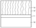
Translated fromKorean도 1a는 종래 기술에 의해 실리콘 기판 상에 질화물 반도체를 성장시키는 것을 나타낸 도면이며, 도 1b는 상기 도 1a에서 성장시킨 질화물 반도체 표면에 대한 SEM 사진이다.FIG. 1A is a view showing growth of a nitride semiconductor on a silicon substrate according to the prior art, and FIG. 1B is a SEM photograph of the nitride semiconductor surface grown in FIG. 1A.
도 2는 본 발명에 의해 실리콘 기판 상에 질화물 반도체를 성장시킨 것을 나타낸 도면이다.2 is a view showing a growth of a nitride semiconductor on a silicon substrate according to the present invention.
도 3a 및 도 3b는 실리콘 기판 상에 버퍼층 및 중간층을 형성시킨 것을 나타낸 도면 및 그 표면에 대한 SEM 사진이다.3A and 3B are views illustrating the formation of a buffer layer and an intermediate layer on a silicon substrate, and SEM images of surfaces thereof.
도 4a 및 도 4b는 실리콘 기판 상에 버퍼층, 중간층 및 평탄화층을 형성시킨 것을 나타낸 도면 및 그 표면에 대한 SEM 사진이다.4A and 4B are views showing the formation of a buffer layer, an intermediate layer, and a planarization layer on a silicon substrate, and SEM images of the surface thereof.
도 5a는 실리콘 기판 상에 버퍼층, 중간층, 평탄화층 및 질화물 반도체층을 형성시킨 것을 나타낸 도면이며, 도 5b 및 도 5c는 실리콘 기판 상에 버퍼층, 중간층, 평탄화층 및 질화물 반도체층을 형성시킨 뒤, 그 표면 및 단면에 대해 찍은 SEM 사진이다.5A is a view showing a buffer layer, an intermediate layer, a planarization layer, and a nitride semiconductor layer formed on a silicon substrate, and FIGS. 5B and 5C illustrate a buffer layer, an intermediate layer, a planarization layer, and a nitride semiconductor layer formed on a silicon substrate. It is a SEM photograph taken about the surface and the cross section.
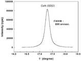
도 6a 및 도 6b는 종래 기술 및 본 발명에 의해 성장시킨 질화물 반도체의 구조에 대해 HRXRD(High Resolution X-Ray Diffraction) 분석을 한 그래프이다.6A and 6B are graphs of HRXRD (High Resolution X-Ray Diffraction) analysis of the structure of the nitride semiconductor grown by the prior art and the present invention.
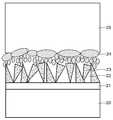
도 7은 본 발명에 의해 제조된 발광 소자의 구조를 나타낸 도면이다.7 is a view showing the structure of a light emitting device manufactured by the present invention.
< 도면의 주요 부분에 대한 부호의 설명 ><Description of Symbols for Main Parts of Drawings>
10, 20, 30, 70... Si 기판 11, 21, 31, 71... 버퍼층10, 20, 30, 70 ... Si substrate 11, 21, 31, 71 ... buffer layer
12, 25, 35, 75... 질화물 반도체층 13... 크랙(내부 결함)12, 25, 35, 75 ...
22, 32, 72... 보이드(void) 23, 33, 73... 중간층22, 32, 72
24, 34, 74... 평탄화층 25, 35, 75, 77... 질화물 반도체층24, 34, 74
76... 활성층 78, 79... 전극층76 ...
본 발명은 실리콘 기판 상에 질화물계 화합물 반도체 및 그 성장시키는 방법에 관한 것으로, 보다 상세하게는 실리콘 기판과 질화물계 화합물 반도체층 사이에 중간층을 성장시켜, 상기 실리콘 기판상에 형성되는 질화물계 화합물 반도체층의 격자 결함, 크랙(crack)의 발생을 저지하는 질화물 반도체 및 그 제조 방법에 관한 것이다.The present invention relates to a nitride compound semiconductor and a method for growing the same on a silicon substrate, and more particularly, a nitride compound semiconductor formed on the silicon substrate by growing an intermediate layer between the silicon substrate and the nitride compound semiconductor layer. The present invention relates to a nitride semiconductor that prevents lattice defects and cracks in a layer, and a method of manufacturing the same.
종래의 청녹색 발광 소자는 GaN 기판의 제조가 어려워서 사파이어 또는 SiC 기판을 이용하여, 그 상부에 화합물 반도체층을 형성시켜왔다. 그러나, 상기 사파이어 또는 SiC 기판을 사용하는 경우에는, 그 비용이 고가이며, 전기 전도도 및 열 전도도가 낮고, 대면적의 성장이 불가능하여 소자의 대량 생산이 어려운 단점이 있다. 또한, 그 자체로 절연체이기 때문에 광전자 특성을 지니는 소자에만 그 응용이 가능하여 광전 특성 및 전기 전자 복합 특성을 가지는 MEMS, NEMS 및 micro-OEIC 소자의 제작이 불가능하다. 이에 비해 실리콘(Si) 기판의 경우, 이러한 단점을 보완할 수 있어 최첨단 광전자 소자 이외의 다양한 소자의 기판으로 사용될 수 있다.Conventional blue-green light emitting devices have been difficult to manufacture GaN substrates, so that compound semiconductor layers have been formed thereon using sapphire or SiC substrates. However, in the case of using the sapphire or SiC substrate, the cost is expensive, the electrical conductivity and the thermal conductivity is low, the large-area growth is impossible, the mass production of the device is difficult. In addition, since it is an insulator itself, the present invention can be applied only to devices having optoelectronic properties, and thus it is impossible to manufacture MEMS, NEMS, and micro-OEIC devices having photoelectric properties and electric / electronic composite properties. On the other hand, in the case of a silicon (Si) substrate, this disadvantage can be compensated for and can be used as a substrate for various devices other than the state-of-the-art optoelectronic devices.
그러나, 상기와 같은 장점에도 불구하고 상기 Si 기판 상에 GaN 와 같은 Ⅲ 족 질화물계 반도체층을 형성시키는 경우 문제가 발생한다. 즉, Si 기판과 GaN 사이의 열전달 계수(thermal expansion coefficient)의 차이(GaN:5.59×10⁻⁶/K, Si:3.59×10⁻⁶/K)로 인하여 고온에서 성장을 시킨 후 냉각시 인장 응력(tensile stress)이 발생하여 성장된 GaN층 내에 결정 결함, 전위, 크랙 등이 발생된다. 특히, 이러한 크랙은 결정의 내부 구조를 취약하게 하여 결국 소자 특성을 악화시키게 되어 Si 기판을 3족 질화물 반도체 성장에 사용하는 것이 어렵게 된다.However, in spite of the above advantages, a problem occurs when forming a group III nitride semiconductor layer such as GaN on the Si substrate. In other words, due to the difference in thermal expansion coefficient (GaN: 5.59 × 10⁻⁶ / K, Si: 3.59 × 10⁻⁶ / K) between the Si substrate and GaN, the tensile stress during cooling after growth at high temperature (tensile stress) occurs and crystal defects, dislocations, cracks, and the like occur in the grown GaN layer. In particular, such cracks weaken the internal structure of the crystals and eventually deteriorate device characteristics, making it difficult to use Si substrates for growth of group III nitride semiconductors.
이러한 단점을 보완하기 위한 노력으로 저온 AlN 버퍼층 성장(LT-AlN : A. Watanabe et al., J. Cryst. Growth 128. 391(1993)), 저온 GaN 버퍼층 성장(LT-GaN : H. Ishikawa et al,. J. Cryst. Growth 189/190, 178 (1998)), 조성이 다른 버퍼층을 연속적으로 다수 반복적으로 성장시켜 초격자(super lattice)를 형성하여 크랙을 줄이는 등의 시도가 있었으나, 크랙의 완전한 제어는 불가능하다.In an effort to compensate for these shortcomings, low temperature AlN buffer layer growth (LT-AlN: A. Watanabe et al., J. Cryst. Growth 128. 391 (1993)), low temperature GaN buffer layer growth (LT-GaN: H. Ishikawa et. al, J. Cryst.Growth 189/190, 178 (1998)), attempting to reduce cracks by forming super lattice by repeatedly growing a large number of buffer layers of different compositions in succession. Full control is not possible.
또한, ELOG이나 PENDO와 같은 ex situ 방법(Y. Kawaguchi et al., Jpn. J. Appl. Phys. 37, L966 (1998))이 시도되었으나 크랙 형성의 완전한 제어가 불가능하고, 또한 소자의 제조 공정이 복잡해져 비용면에서도 불리한 단점이 있다.In addition, ex situ methods such as ELOG or PENDO (Y. Kawaguchi et al., Jpn. J. Appl. Phys. 37, L966 (1998)) have been attempted but complete control of crack formation is not possible and also the manufacturing process of the device. This complexity is disadvantageous in terms of cost.
도 1a에서는 종래 기술에 의해 Si 기판 상에 Ⅲ 족 질화물계 반도체층을 형 성시킨 것을 나타내었다. 즉, Si 기판(10) 상에 버퍼층(buffer layer : 완충층)(11)을 형성시키고, 상기 버퍼층(11)상에 고온에서 GaN(12)을 형성시켰다. 이러한 버퍼층(11)은 상기 Si 기판(10) 및 GaN(12)의 열전도 및 결정 구조를 고려한 물질이 선택되어 GaN(12)을 보다 안정적으로 성장시키기 위해 사용되었다. 그러나, 이러한 경우에도 상기 GaN(12) 내부에 발생하는 격자 결함, 전위(dislocation) 및 크랙(13)의 완전한 제어가 어렵게 된다. 이를 도 1b에 나타내었다. 도 1b는 상기 도 1a와 같이 형성시킨 GaN(12)의 표면에 대한 SEM 사진이다. 도면을 참조하며, 그 표면에 수많은 결정 결함(13)들이 생겨난 것을 알 수 있다. 이러한 결정 결함은 결과적으로 완성된 반도체 소자의 성질을 악화시키는 원인이 된다.In FIG. 1A, a group III nitride semiconductor layer is formed on a Si substrate by a conventional technique. That is, a
본 발명에서는 상기 문제점을 해결하기 위하여, 제조 공정 도중 Si 기판과 질화물 반도체 사이에 발생할 수 있는 인장응력(tensile stress)을 감소시키거나 소멸시킴으로써 상기 질화물 반도체 내부의 결정 결함, 전위 또는 크랙의 발생을 크게 감소시킨 질화물 반도체 및 그 제조 방법을 제공하는 것을 목적으로 한다.In order to solve the above problems, the present invention greatly reduces the occurrence of crystal defects, dislocations or cracks in the nitride semiconductor by reducing or eliminating tensile stress that may occur between the Si substrate and the nitride semiconductor during the manufacturing process. It is an object to provide a reduced nitride semiconductor and a method of manufacturing the same.
본 발명에서는 상기 목적을 달성하기 위하여,In the present invention, to achieve the above object,
실리콘 기판;Silicon substrates;
상기 실리콘 기판 상에 형성되며 보이드(void)를 함유한 중간층;An intermediate layer formed on the silicon substrate and containing a void;
상기 중간층 상에 형성된 평탄화층; 및A planarization layer formed on the intermediate layer; And
상기 평탄화층 상에 형성된 질화물 반도체층;을 포함하는 실리콘 기판 상에 형성된 질화물 반도체를 제공한다.It provides a nitride semiconductor formed on a silicon substrate comprising a; nitride semiconductor layer formed on the planarization layer.
본 발명에 있어서, 상기 기판 및 상기 중간층 사이에 형성된 버퍼층을 더 포함하는 것이 바람직하다.In the present invention, it is preferable to further include a buffer layer formed between the substrate and the intermediate layer.
본 발명에 있어서, 상기 중간층, 평탄화층 및 질화물 반도체층은 Ⅲ족 질화물계 화합물 반도체 물질을 포함한다.In the present invention, the intermediate layer, the planarization layer and the nitride semiconductor layer include a group III nitride compound semiconductor material.
본 발명에 있어서, 상기 평탄화층은 약 100nm 내지 500nm의 두께로 형성되는 것이 바람직하다.In the present invention, the planarization layer is preferably formed to a thickness of about 100nm to 500nm.
또한, 본 발명에서는In the present invention,
실리콘 기판;Silicon substrates;
상기 실리콘 기판 상에 형성되며 보이드(void)를 함유한 중간층;An intermediate layer formed on the silicon substrate and containing a void;
상기 중간층 상에 형성된 평탄화층;A planarization layer formed on the intermediate layer;
상기 평탄화층 상에 형성된 제 1질화물 반도체층;A first nitride semiconductor layer formed on the planarization layer;
상기 제 1질화물 반도체층의 일부위에 순차적으로 형성된 활성층, 제 2질화물 반도체층, 제 1전극층; 및An active layer, a second nitride semiconductor layer, and a first electrode layer sequentially formed on a portion of the first nitride semiconductor layer; And
상기 제 1질화물 반도체층의 상기 활성층이 형성되지 않은 부위에 형성된 제 2전극층을 포함하는 발광소자를 제공한다.Provided is a light emitting device including a second electrode layer formed on a portion where the active layer of the first nitride semiconductor layer is not formed.
또한, 본 발명에서는 실리콘 기판 상에 질화물계 반도체의 형성 방법에 있어서,Moreover, in this invention, in the method of forming a nitride type semiconductor on a silicon substrate,
(가) 실리콘 기판 상에 보이드(void)가 포함된 중간층을 형성시키는 단계;(A) forming an intermediate layer containing voids on the silicon substrate;
(나) 상기 중간층 상에 평탄화층을 형성시키는 단계; 및(B) forming a planarization layer on the intermediate layer; And
(다) 상기 평탄화층 상에 질화물계 반도체층을 형성시키는 단계;를 포함하는 실리콘 기판 상의 질화물 반도체 제조 방법을 제공한다.(C) forming a nitride-based semiconductor layer on the planarization layer provides a method for manufacturing a nitride semiconductor on a silicon substrate.
본 발명에 있어서, 실리콘 기판 및 중간층 사이에 버퍼층을 형성하는 단계;를 더 포함하는 것이 바람직하다.In the present invention, it is preferable to further include; forming a buffer layer between the silicon substrate and the intermediate layer.
본 발명에 있어서, 상기 (가) 단계는 섭씨 약 700도 내지 900도에서 이루어지고, 상기 (나) 단계는 섭씨 약 500도 내지 700도에서 이루어지며, 상기 (다) 단계는 섭씨 약 900도 내지 1200도에서 이루어질 수 있다.In the present invention, the (a) step is performed at about 700 degrees to 900 degrees Celsius, the (b) step is performed at about 500 degrees to 700 degrees Celsius, and the (c) step is about 900 degrees Celsius to It can be made at 1200 degrees.
상기 평탄화층은 약 100 내지 500nm의 두께로 형성되며, 상기 단계들은 MOCVD 공정에 의해 이루어질 수 있다.The planarization layer is formed to a thickness of about 100 to 500nm, the steps may be made by a MOCVD process.
이하, 도면을 참조하면서 본 발명에 의한 실기콘 기판 상에 형성시킨 질화물계 반도체에 대해 보다 상세히 설명하기로 한다. 도 2는 본 발명에 의해 Si 기판 상에 성장시킨 질화물 반도체를 나타낸 도면이다. 도 2를 참조하면, Si 기판(20) 상에 버퍼층(21)이 형성되어 있으며, 상기 버퍼층(21) 상에 보이드(22)를 포함하는 중간층(23)이 형성된다. 그리고, 상기 보이드(22)를 포함하는 중간층(23) 상에 평탄화층(24)이 형성되며, 마지막으로 상기 평탄화층(24) 상에 질화물계 화합물(25)이 형성된 구조를 가진다.Hereinafter, the nitride-based semiconductor formed on the silicon substrate according to the present invention with reference to the drawings will be described in more detail. 2 shows a nitride semiconductor grown on a Si substrate according to the present invention. Referring to FIG. 2, a
본 발명에 있어서, 상기 버퍼층(21)은 상기 질화물 반도체 물질(25), 예를 들어 GaN이 상기 Si 기판(20)에 대한 젖음(wetting)성이 부족하기 때문에 이를 보완하기 위해서 형성시킨 것이다. 여기서 젖음성이란, 한 물질(기지 물질) 상부에 다른 물질을 형성시키는 경우, 얼마나 일정한 면밀도를 가지고 형성되는가를 나타낸 것으로 젖음성이 부족한 경우에는 기지 물질 상에서 특정 부위에만 성장이 일어나기 때문에 평탄화가 쉽지 않게 된다. 일반적으로 Si 기판(20) 상에 GaN과 같은 질화물계 화합물을 바로 형성시킬 때, 그들 사이에 완충층의 역할을 하는 버퍼층(21)을 형성시킨다. 이러한 버퍼층(21)은 한정되지 않으며, 형성되는 화합물 반도체의 종류에 따라 선택될 수 있다.In the present invention, the
상기 버퍼층(21) 상에는 보이드(22)를 포함하는 중간층(23)이 형성되어 있다. 상기 중간층(23)은 Ⅲ족 질화물계 물질로 이루어진다. 상기 중간층(23)은 보이드(22)를 포함하고 있으며, 이는 인위적으로 상기 중간층(23)의 형성 조건을 조절하여 이루어진 것이다.The
상기 중간층(23) 상에는 평탄화층(24)이 형성된다. 평탄화층(24) 역시, 상기 중간층(23)과 마찬가지로 질화물 반도체 물질로 이루어진다. 이러한 평탄화층(24)은 그 상부에 형성될 질화물 반도체층(25)이 고른 분포의 안정한 상태로 형성되기 위한 것으로 그 하부에 형성된 중간층(23)과는 달리 상대적으로 큰 보이드(22)를 포함하지는 않으나, 미소한 크기의 보이드가 포함될 수 있다.The
상기 평탄화층(24) 상에 질화물 반도체층(25)이 형성되어 있다. 이와 같이 형성시킨 구조의 질화물 반도체는 도 1a의 종래 기술에 의한 질화물 반도체와는 달리, 질화물 반도체층(25)이 결정 결함, 전위(dislocation) 및 크랙 등의 발생이 억제된다. 이는 상기 중간층(23) 내에 형성된 보이드(22)가 Si 기판(20)과 질화물 반도체층(25) 사이에서 발생될 수 있는 인장응력를 감소시키고, 상기 버퍼층(23) 및 상기 평탄화층(24)이 완충적인 역할을 하기 때문에 질화물 반도체층(25)이 매우 안정적으로 성장할 수 있는 것이다.The
상기와 같은 구조의 Si 기판 상에 형성된 질화물계 반도체의 형성 방법을 설명하면 다음과 같다.Referring to the method of forming the nitride-based semiconductor formed on the Si substrate of the above structure as follows.
먼저, Si 기판(20) 상에 버퍼층(21)을 형성시킨다. 상기 버퍼층(21)은 상기 Si 기판(20)에 대한 젖음성을 향상시키기 위한 것으로, 상기 버퍼층(21)을 구성하는 물질에 따라 적절한 두께로 성장시킨다.First, the
다음으로, 상기 버퍼층(21) 상부에 보이드(22)를 포함하는 중간층(23)을 형성시킨다. 상기 중간층(23)은 Ⅲ족 질화물계 물질로 이루어진다. 상기 중간층(23)을 구성하는 물질이 GaN인 경우에는 섭씨 약 700도 내지 섭씨 약 900도 사이의 온도에서 형성시키는 것이 바람직하다. 이 경우, 상기 중간층(23)은 상기 Si 기판(20)에 대한 젖음성이 부족한 관계로 도 2에 나타낸 바와 같이, 피라미드 형상으로 성장된다. 또한, 그 표면은 굴곡이 매우 심하여 거칠기(roughness)가 매우 큰 상태로 성장된다. 따라서, 상기 중간층(23)의 내부에 다수의 보이드(22)가 형성된다.Next, an
다음으로, 상기 중간층(23) 상부에 평탄화층(24)을 형성시킨다. 상기 평탄화층(24)은 Ⅲ족 질화물계 물질을 포함하여 형성된다. 상기 평탄화층(24)을 구성하는 물질이 GaN인 경우에는 섭씨 약 500도 내지 섭씨 약 700도 사이의 온도에서 형성시키는 것이 바람직하다. 이때, 상기 평탄화층(24)의 두께는 약 100 내지 500nm로 성장시키며, 보다 바람직하게는 약 200 내지 400nm의 두께로 성장시킨다. 상기 중간층(23) 상에 이러한 평탄화층(24)을 성장시킴에 따라 그 표면이 굴곡이 점차 사라지게 되며, 최종적으로 평탄화된 표면을 얻을 수 있다.Next, the
마지막으로, 상기 평탄화층(24) 상부에 질화물 반도체층(25)을 형성시킨다. 상기 질화물 반도체층(25)은 그 용도에 따라 형성 두께를 조절할 수 있으며, 일반적으로 수 ㎛로 성장시킨다. 상기 질화물 반도체층(25)을 구성하는 물질이 GaN인 경우에 성장 온도는 섭씨 약 900도 내지 1200도로 유지하는 것이 바람직하다. 이와 같이 성장된 질화물 반도체층(25)은 Si 기판(20) 사이의 계면에서 형성된 인장 응력이 그 사이에 형성된 중간층(23) 내부의 보이드(22)에 의해 감소되어, 상기 공정 후 냉각하는 과정에서 발생하는 결정 결함, 전위(dislocation) 또는 크랙을 억제할 수 있다.Finally, the
상기와 같은 방법에 의해 본 발명에 의한 실기콘 기판 상에 질화물 반도체를 MOCVD(Metal-Organic Chemical Vapor Deposition) 공정으로 형성시키는 과정에 대해 단계별로 SEM 사진을 촬영하였다.SEM photographs were taken step by step for the formation of the nitride semiconductor on the silicon substrate according to the present invention by the method as described above by the MOCVD (Metal-Organic Chemical Vapor Deposition) process.
도 3a 및 도 3b를 참조하면, Si 기판(30) 상에 GaN(35)을 형성시키기 전에 상기 GaN(35)의 상기 Si 기판(30)에 대한 젖음성을 향상시키기 위한 버퍼층(31)을 형성시킨다. 다음으로 섭씨 약 800 도에서 중간층(33)으로 GaN을 성장시킨다. 성장시킨 두께는 약 300nm이다. 이 경우, 중간층(33)으로 성장시킨 GaN은 상기 Si 기판(31)에 대한 젖음성이 부족해서 에피탁샬 성장은 어렵게 되어 도 3a에 나타낸 바와 같은 피라미드형 구조를 나타내며 표면 거칠기가 매우 심한 형태를 나타낸다. 따라서 중간층(33) 내부에 보이드(32)가 형성된다.Referring to FIGS. 3A and 3B, before forming
도 3b에서는 이와 같이 중간층(33)을 성장시킨 뒤, 그 표면에 대해 촬영한 SEM 사진을 나타낸 것이다. 사진에 나타낸 바와 같이, 중간층(33) 표면은 매우 거칠게 되며, 어두운 부분으로 나타난 보이드의 밀도가 매우 높은 것을 알 수 있다. 그리고, 상기 중간층(33)까지 형성시킨 뒤, 그 단면에 대해 찍은 SEM 사진을 도 3c에 나타내었다. 도 3c를 참조하면, 기판(31) 상에 형성시킨 보이드(32)를 포함하는 중간층(33)이 다른 층보다 밝은 형태로 인식할 수 있다.In FIG. 3B, after the
다음으로 도 4a에 나타낸 바와 같이, 상기 중간층(33) 상부에 평탄화층(34)으로 GaN을 성장시킨다. 이때의 온도는 상기 중간층(33) 성장 온도 보다 낮은 섭씨 약 560 도 정도이며, 그 두께는 약 300nm 정도이다. 상기 중간층(33)의 형성 온도보다 낮은 온도에서 형성되는 평탄화층(34)은 그 하부의 중간층(33)내에 형성된 ㅂ보이드(32)를 완전히 채우지 않은 상태에서 성장한다. 이와 같이 성장시키는 평탄화층(34)의 표면에 대해 촬영한 SEM 사진을 도 4b에 나타내었다. 도 4b를 참조하면, 보이드(32)를 포함한 중간층(33) 상에 평탄화층(34)이 점차 성장해가는 것을 살펴볼 수 있다. 즉, 상기 평탄화층(34)이 그 도포된 면적을 넓혀 가면서 상기 중간층(33) 상부를 덮으면서 평탄화되어 가는 것이다.Next, as shown in FIG. 4A, GaN is grown to the
마지막으로 도 5a에 나타낸 바와 같이, 상기 평탄화층(34) 상부에 질화물 반도체층(35)을 형성시킨다. 이때의 성장 온도는 고온인 섭씨 약 1050 도였으며, 성장 두께도 수 ㎛였다. 질화물 반도체층(35)을 형성시킨 뒤, 그 표면에 대해 촬영한 SEM 사진을 도 5b에 나타내었으며, 본 발명에 의해 크랙의 형성이 억제되었음을 알 수 있다. 상기 중간층(33)에 형성된 보이드(32)의 영향으로 질화물 반도체층(35) 내부의 인장응력은 이완되어 안정된 구조를 나타내게 된다. 그리고, 상기 질화물 반도체층(35)을 형성시킨 뒤, 그 단면에 대한 SEM 사진을 촬영하였다. 이를 도 5c에 나타내었다. 도 5c를 참조하면, 상기 도 3c와 같이 명확하게 관찰되지는 않으나, 실리콘 기판(30)과 질화물 반도체층(35) 사이에 보이드(32)가 형성된 중간층(33)을 확인할 수 있다.Finally, as shown in FIG. 5A, the
상기한 과정을 거쳐 제조된 구조에 대한 분석을 위하여, HRXRD(High Resolution X-Ray Diffraction : 고분해능 X-ray 회절)실험을 실시하여, 상기 도 1a의 종래 기술에 의한 반도체 구조와 비교하였다. 이를 도 6a 및 도 6b에 나타내었다. 도 6a 및 도 6b를 참조하면, 종래 기술에 의해 성장된 GaN의 (002) 방향의 X-ray 회절 강도는 5800cps(도 6a)이며, 본 발명에 의해 성장된 GaN의 (002) 방향의 X-ray 회절 강도는 8200cps(도 6b)이다. 그리고, FWHM(Full Width Half Maximum) 값도 종래 기술인 도 6a의 경우 1155arcsec이고, 본 발명인 도 6b의 경우 690arcsec로서 본 발명에 의해 성장된 GaN의 결정 성장이 종래 기술에 비해 매우 안정적으로 이루어져 결정성이 향상되는 것을 알 수 있다.In order to analyze the structure manufactured through the above process, HRXRD (High Resolution X-Ray Diffraction) experiment was performed and compared with the semiconductor structure according to the prior art of FIG. 1A. This is shown in Figures 6a and 6b. 6A and 6B, the X-ray diffraction intensity in the (002) direction of GaN grown by the prior art is 5800 cps (FIG. 6A), and the X- in the (002) direction of GaN grown by the present invention. The ray diffraction intensity is 8200 cps (FIG. 6B). Also, the Full Width Half Maximum (FWHM) value is 1155 arcsec in the case of FIG. 6A, and 690 arcsec in the case of FIG. 6B, and the crystal growth of GaN grown by the present invention is more stable than in the prior art. It can be seen that the improvement.
도 7은 본 발명에 의한 질화물 반도체를 발광 소자에 응용한 실시예를 나타낸다. 이를 설명하면 다음과 같다. 기판(70) 상에 버퍼층(71)이 형성되어 있으며, 상기 버퍼층(71) 상에 보이드(72)를 포함하는 중간층(73)이 형성된다. 그리고, 상기 중간층(73) 상에 평탄화층(74)이 형성되며, 상기 평탄화층(74) 상에 안정화된 질화물계 화합물(75)이 형성된다. 여기서, 상기 질화물계 화합물이 n-type으로 형성된 경우, 상기 n-질화물계 화합물층(75) 상부의 일 부위에 활성층(76), p-질화물계 화합물층(77) 및 p-전극층(78)이 순차적으로 형성된다. 그리고, 상기 n-질화물계 화합물층(75) 상부의 상기 활성층이 형성되지 않은 부위에 n-전극층(79)이 형성된다. 상기 보이드(72)를 포함하는 중간층(73) 상에 크랙이 없고 격자 결함 및 전위 밀도가 감소되어 결정성이 향상된 질화물계 화합물 반도체층들을 형성시킴으로써 고성능, 고수율의 질화물계 화합물 반도체 소자를 구현할 수 있다.7 shows an embodiment in which the nitride semiconductor according to the present invention is applied to a light emitting device. This is described as follows. A
상기한 설명에서 많은 사항이 구체적으로 기재되어 있으나, 그들은 발명의 범위를 한정하는 것이라기보다, 바람직한 실시예의 예시로서 해석되어야 한다. 본 발명의 범위는 설명된 실시예에 의하여 정하여 질 것이 아니고 특허 청구범위에 기재된 기술적 사상에 의해 정하여져야 한다.While many details are set forth in the foregoing description, they should be construed as illustrative of preferred embodiments, rather than to limit the scope of the invention. The scope of the invention should not be defined by the described embodiments, but should be determined by the technical spirit described in the claims.
본 발명에 의하면, 제조 공정 도중 Si 기판과 질화물 반도체 사이에 발생할 수 있는 인장응력을 이완하여 상기 질화물 반도체 내부의 결정 결함, 전위 또는 크랙의 발생을 크게 감소시킨 질화물 반도체를 제공할 수 있다.According to the present invention, it is possible to provide a nitride semiconductor which greatly reduces the occurrence of crystal defects, dislocations or cracks in the nitride semiconductor by relaxing tensile stress that may occur between the Si substrate and the nitride semiconductor during the manufacturing process.
이에 의해, 1) 저가의 Si 기판을 기술적인 불이익 없이 사용할 수 있으므로 제조 비용이 감소하고, 2) 대면적의 Si 기판을 사용할 수 있으므로 제조 비용이 감소하고, 3) 전기 전도도 및 열전도도가 우수한 Si 기판을 사용함으로써 소자의 정전 내압 향상 및 내열 특성이 향상되어 신뢰도와 수명이 증가하고, 4) 광전 특성 및 전기 전자 복합 특성을 지닌 최첨단 정보 광전 소자로의 응용 가능성이 커지게 된다.As a result, 1) low-cost Si substrates can be used without technical penalties, thereby reducing manufacturing costs; 2) large-area Si substrates can be used to reduce manufacturing costs; and 3) Si with excellent electrical and thermal conductivity. The use of the substrate improves the electrostatic breakdown voltage and heat resistance of the device, thereby increasing reliability and lifespan.
Claims (16)
Translated fromKoreanPriority Applications (4)
| Application Number | Priority Date | Filing Date | Title |
|---|---|---|---|
| KR1020030070984AKR100744933B1 (en) | 2003-10-13 | 2003-10-13 | A nitride semiconductor formed on a silicon substrate and a method of manufacturing the same |
| US10/949,469US20050077512A1 (en) | 2003-10-13 | 2004-09-27 | Nitride semiconductors on silicon substrate and method of manufacturing the same |
| JP2004297529AJP2005123619A (en) | 2003-10-13 | 2004-10-12 | Nitride semiconductor formed on silicon substrate and manufacturing method thereof |
| CNB2004100850229ACN100452449C (en) | 2003-10-13 | 2004-10-13 | Nitride semiconductors on silicon substrate and method of manufacturing the same |
Applications Claiming Priority (1)
| Application Number | Priority Date | Filing Date | Title |
|---|---|---|---|
| KR1020030070984AKR100744933B1 (en) | 2003-10-13 | 2003-10-13 | A nitride semiconductor formed on a silicon substrate and a method of manufacturing the same |
Publications (2)
| Publication Number | Publication Date |
|---|---|
| KR20050035565A KR20050035565A (en) | 2005-04-19 |
| KR100744933B1true KR100744933B1 (en) | 2007-08-01 |
Family
ID=34420627
Family Applications (1)
| Application Number | Title | Priority Date | Filing Date |
|---|---|---|---|
| KR1020030070984AExpired - Fee RelatedKR100744933B1 (en) | 2003-10-13 | 2003-10-13 | A nitride semiconductor formed on a silicon substrate and a method of manufacturing the same |
Country Status (4)
| Country | Link |
|---|---|
| US (1) | US20050077512A1 (en) |
| JP (1) | JP2005123619A (en) |
| KR (1) | KR100744933B1 (en) |
| CN (1) | CN100452449C (en) |
Cited By (4)
| Publication number | Priority date | Publication date | Assignee | Title |
|---|---|---|---|---|
| WO2010027230A3 (en)* | 2008-09-08 | 2010-07-08 | 서울대학교 산학협력단 | Structure of thin nitride film and formation method thereof |
| KR101020473B1 (en) | 2008-11-26 | 2011-03-08 | 한국광기술원 | Light emitting device and manufacturing method |
| US8466472B2 (en) | 2010-12-17 | 2013-06-18 | Samsung Electronics Co., Ltd. | Semiconductor device, method of manufacturing the same, and electronic device including the semiconductor device |
| KR101466037B1 (en)* | 2011-12-15 | 2014-11-28 | 서울대학교산학협력단 | Substrate for semiconductor device, nitride thin film structure using the same and method of forming the same |
Families Citing this family (27)
| Publication number | Priority date | Publication date | Assignee | Title |
|---|---|---|---|---|
| JP4826703B2 (en)* | 2004-09-29 | 2011-11-30 | サンケン電気株式会社 | Plate-like substrate for use in forming semiconductor elements |
| WO2009128646A2 (en)* | 2008-04-16 | 2009-10-22 | Lumigntech Co., Ltd. | Semiconductor substrate and method for manufacturing the same |
| KR101046144B1 (en)* | 2008-10-21 | 2011-07-01 | 삼성엘이디 주식회사 | Gallium nitride film production method and nitride-based heterojunction field effect transistor manufacturing method |
| KR101047617B1 (en)* | 2009-05-21 | 2011-07-07 | 엘지이노텍 주식회사 | Semiconductor light emitting device and manufacturing method thereof |
| WO2010143778A1 (en) | 2009-06-10 | 2010-12-16 | 서울옵토디바이스주식회사 | Semiconductor substrate, fabrication method thereof, semiconductor device and fabrication method thereof |
| US8860183B2 (en) | 2009-06-10 | 2014-10-14 | Seoul Viosys Co., Ltd. | Semiconductor substrate, semiconductor device, and manufacturing methods thereof |
| US8481411B2 (en) | 2009-06-10 | 2013-07-09 | Seoul Opto Device Co., Ltd. | Method of manufacturing a semiconductor substrate having a cavity |
| KR101087901B1 (en) | 2009-08-11 | 2011-11-30 | 한국광기술원 | Nitride semiconductor light emitting device and manufacturing method |
| JP5847083B2 (en) | 2009-08-26 | 2016-01-20 | ソウル バイオシス カンパニー リミテッドSeoul Viosys Co.,Ltd. | Method for manufacturing light emitting device |
| KR101082788B1 (en)* | 2009-10-16 | 2011-11-14 | 한국산업기술대학교산학협력단 | High Quality Non-polar/Semi-polar Semiconductor Device on Porous Nitride Semiconductor and Manufacturing Method thereof |
| JP5570838B2 (en) | 2010-02-10 | 2014-08-13 | ソウル バイオシス カンパニー リミテッド | Semiconductor substrate, manufacturing method thereof, semiconductor device and manufacturing method thereof |
| CN102376830B (en)* | 2010-08-19 | 2015-07-08 | 展晶科技(深圳)有限公司 | Light emitting diode and manufacturing method thereof |
| US20130200391A1 (en)* | 2010-09-28 | 2013-08-08 | North Carolina State University | Gallium nitride based structures with embedded voids and methods for their fabrication |
| KR20120032329A (en)* | 2010-09-28 | 2012-04-05 | 삼성전자주식회사 | Semiconductor device |
| KR101638975B1 (en)* | 2010-10-26 | 2016-07-12 | 삼성전자주식회사 | Nitride-based semiconductor substrate having hollow member pattern and method of fabricating the same |
| US20120105385A1 (en)* | 2010-11-02 | 2012-05-03 | Qualcomm Mems Technologies, Inc. | Electromechanical systems apparatuses and methods for providing rough surfaces |
| KR20120079393A (en)* | 2011-01-04 | 2012-07-12 | (주)세미머티리얼즈 | A method for manufacturing semiconductor light emitting device |
| KR101761309B1 (en)* | 2011-04-19 | 2017-07-25 | 삼성전자주식회사 | GaN film structure, method of fabricating the same and semiconductor device including the same |
| KR101773091B1 (en)* | 2011-05-20 | 2017-08-30 | 엘지이노텍 주식회사 | A light emitting device and a method of fabricating the same |
| US20140158976A1 (en) | 2012-12-06 | 2014-06-12 | Sansaptak DASGUPTA | Iii-n semiconductor-on-silicon structures and techniques |
| WO2015025631A1 (en)* | 2013-08-21 | 2015-02-26 | シャープ株式会社 | Nitride semiconductor light-emitting element |
| KR102122846B1 (en)* | 2013-09-27 | 2020-06-15 | 서울바이오시스 주식회사 | Method for growing nitride semiconductor, method of making template for fabricating semiconductor and method of making semiconductor light-emitting device using the same |
| CN103928583B (en)* | 2014-04-29 | 2017-06-13 | 中国科学院上海微系统与信息技术研究所 | A kind of preparation method of GaN single crystal self-supported substrate |
| US9337023B1 (en)* | 2014-12-15 | 2016-05-10 | Texas Instruments Incorporated | Buffer stack for group IIIA-N devices |
| US11699586B2 (en)* | 2019-08-13 | 2023-07-11 | Enkris Semiconductor, Inc. | Method of manufacturing nitride semiconductor substrate |
| CN113508467A (en)* | 2021-03-30 | 2021-10-15 | 英诺赛科(苏州)科技有限公司 | Group III-nitride semiconductor devices on patterned substrates |
| US12324179B2 (en)* | 2021-12-16 | 2025-06-03 | Wolfspeed, Inc. | Group III-nitride high-electron mobility transistors with a buried metallic conductive material layer and process for making the same |
Citations (4)
| Publication number | Priority date | Publication date | Assignee | Title |
|---|---|---|---|---|
| JP2001223165A (en) | 2000-02-10 | 2001-08-17 | Hitachi Cable Ltd | Nitride semiconductor and manufacturing method thereof |
| JP2002175985A (en)* | 2000-12-05 | 2002-06-21 | Hitachi Cable Ltd | Method for manufacturing nitride semiconductor epitaxial wafer and nitride semiconductor epitaxial wafer |
| JP2003046199A (en) | 2001-07-27 | 2003-02-14 | Canon Inc | Fabrication method and structure of II-VI device using porous membrane |
| JP2003086508A (en) | 2001-09-12 | 2003-03-20 | Canon Inc | Compound semiconductor layer substrate, method of manufacturing the same, and device manufactured on the substrate |
Family Cites Families (15)
| Publication number | Priority date | Publication date | Assignee | Title |
|---|---|---|---|---|
| US5523589A (en)* | 1994-09-20 | 1996-06-04 | Cree Research, Inc. | Vertical geometry light emitting diode with group III nitride active layer and extended lifetime |
| JPH0992882A (en)* | 1995-09-25 | 1997-04-04 | Mitsubishi Electric Corp | Semiconductor light emitting device and manufacturing method thereof |
| US6677619B1 (en)* | 1997-01-09 | 2004-01-13 | Nichia Chemical Industries, Ltd. | Nitride semiconductor device |
| CN1964094B (en)* | 1997-01-09 | 2012-03-14 | 日亚化学工业株式会社 | Nitride semiconductor device |
| US5927995A (en)* | 1997-04-09 | 1999-07-27 | Hewlett-Packard Company | Reduction of threading dislocations by amorphization and recrystallization |
| JP3257442B2 (en)* | 1997-04-09 | 2002-02-18 | 松下電器産業株式会社 | Method for producing gallium nitride crystal |
| JP3930161B2 (en)* | 1997-08-29 | 2007-06-13 | 株式会社東芝 | Nitride-based semiconductor device, light-emitting device, and manufacturing method thereof |
| US6294159B1 (en)* | 1998-10-09 | 2001-09-25 | Colgate Palmolive Company | Volumizing hair care compositions |
| JP3592553B2 (en)* | 1998-10-15 | 2004-11-24 | 株式会社東芝 | Gallium nitride based semiconductor device |
| JP3786544B2 (en)* | 1999-06-10 | 2006-06-14 | パイオニア株式会社 | Nitride semiconductor device manufacturing method and device manufactured by the method |
| JP2000357820A (en)* | 1999-06-15 | 2000-12-26 | Pioneer Electronic Corp | Gallium nitride based semiconductor light emitting device and method of manufacturing the same |
| JP4432180B2 (en)* | 1999-12-24 | 2010-03-17 | 豊田合成株式会社 | Group III nitride compound semiconductor manufacturing method, group III nitride compound semiconductor device, and group III nitride compound semiconductor |
| JP4595198B2 (en)* | 2000-12-15 | 2010-12-08 | ソニー株式会社 | Semiconductor light emitting device and method for manufacturing semiconductor light emitting device |
| JP3886341B2 (en)* | 2001-05-21 | 2007-02-28 | 日本電気株式会社 | Method for manufacturing gallium nitride crystal substrate and gallium nitride crystal substrate |
| TWI303909B (en)* | 2002-11-25 | 2008-12-01 | Nichia Corp | Ridge waveguide semiconductor laser diode |
- 2003
- 2003-10-13KRKR1020030070984Apatent/KR100744933B1/ennot_activeExpired - Fee Related
- 2004
- 2004-09-27USUS10/949,469patent/US20050077512A1/ennot_activeAbandoned
- 2004-10-12JPJP2004297529Apatent/JP2005123619A/enactivePending
- 2004-10-13CNCNB2004100850229Apatent/CN100452449C/ennot_activeExpired - Fee Related
Patent Citations (4)
| Publication number | Priority date | Publication date | Assignee | Title |
|---|---|---|---|---|
| JP2001223165A (en) | 2000-02-10 | 2001-08-17 | Hitachi Cable Ltd | Nitride semiconductor and manufacturing method thereof |
| JP2002175985A (en)* | 2000-12-05 | 2002-06-21 | Hitachi Cable Ltd | Method for manufacturing nitride semiconductor epitaxial wafer and nitride semiconductor epitaxial wafer |
| JP2003046199A (en) | 2001-07-27 | 2003-02-14 | Canon Inc | Fabrication method and structure of II-VI device using porous membrane |
| JP2003086508A (en) | 2001-09-12 | 2003-03-20 | Canon Inc | Compound semiconductor layer substrate, method of manufacturing the same, and device manufactured on the substrate |
Cited By (6)
| Publication number | Priority date | Publication date | Assignee | Title |
|---|---|---|---|---|
| WO2010027230A3 (en)* | 2008-09-08 | 2010-07-08 | 서울대학교 산학협력단 | Structure of thin nitride film and formation method thereof |
| KR101101780B1 (en)* | 2008-09-08 | 2012-01-05 | 서울대학교산학협력단 | Nitride thin film structure and its formation method |
| US8847362B2 (en) | 2008-09-08 | 2014-09-30 | Snu R&Db Foundation | Structure of thin nitride film and formation method thereof |
| KR101020473B1 (en) | 2008-11-26 | 2011-03-08 | 한국광기술원 | Light emitting device and manufacturing method |
| US8466472B2 (en) | 2010-12-17 | 2013-06-18 | Samsung Electronics Co., Ltd. | Semiconductor device, method of manufacturing the same, and electronic device including the semiconductor device |
| KR101466037B1 (en)* | 2011-12-15 | 2014-11-28 | 서울대학교산학협력단 | Substrate for semiconductor device, nitride thin film structure using the same and method of forming the same |
Also Published As
| Publication number | Publication date |
|---|---|
| KR20050035565A (en) | 2005-04-19 |
| US20050077512A1 (en) | 2005-04-14 |
| CN1607683A (en) | 2005-04-20 |
| CN100452449C (en) | 2009-01-14 |
| JP2005123619A (en) | 2005-05-12 |
Similar Documents
| Publication | Publication Date | Title |
|---|---|---|
| KR100744933B1 (en) | A nitride semiconductor formed on a silicon substrate and a method of manufacturing the same | |
| US7811902B2 (en) | Method for manufacturing nitride based single crystal substrate and method for manufacturing nitride based light emitting diode using the same | |
| CN100380588C (en) | Preparation method of gallium nitride layer | |
| US6403451B1 (en) | Methods of fabricating gallium nitride semiconductor layers on substrates including non-gallium nitride posts | |
| US8475588B2 (en) | Wafer structure and epitaxial growth method for growing the same | |
| CN100382244C (en) | Buffer structure for modifying silicon substrate | |
| CN101978470B (en) | Method for manufacturing a layer of gallium nitride or aluminum nitride | |
| US9252012B2 (en) | Method of fabricating a nitride substrate | |
| JP2004508268A (en) | Method of forming a defect-free, crack-free epitaxial film on a mismatched substrate | |
| US20140001438A1 (en) | Semiconductor devices and methods of manufacturing the same | |
| KR100865600B1 (en) | Gallium nitride semiconductor structure and method for manufacturing same, and semiconductor structure and method for manufacturing same | |
| US9685589B2 (en) | Optoelectronic component with a layer structure | |
| EP2362412B1 (en) | Method of growing nitride semiconductor | |
| JP6165884B2 (en) | Semiconductor laminate and method for producing semiconductor laminate | |
| KR19990016925A (en) | Baline single crystal manufacturing method | |
| An et al. | Heteroepitaxial Growth of High‐Quality GaN Thin Films on Si Substrates Coated with Self‐Assembled Sub‐micrometer‐sized Silica Balls | |
| CN114892264A (en) | Gallium nitride substrate, gallium nitride single crystal layer and method for producing the same | |
| JP2003178977A (en) | Semiconductor crystal and manufacturing method thereof | |
| Chang et al. | A GeSi-buffer structure for growth of high-quality GaAs epitaxial layers on a Si substrate | |
| JP7479707B2 (en) | III-N semiconductor structure and method for producing same | |
| JP7207588B1 (en) | III-nitride semiconductor wafer and manufacturing method thereof | |
| KR101466037B1 (en) | Substrate for semiconductor device, nitride thin film structure using the same and method of forming the same | |
| WO2023119916A1 (en) | Nitride semiconductor substrate and method for manufacturing nitride semiconductor substrate | |
| JP2023092416A (en) | Nitride semiconductor substrate and method for manufacturing nitride semiconductor substrate | |
| KR19990049361A (en) | GAN single crystal manufacturing method |
Legal Events
| Date | Code | Title | Description |
|---|---|---|---|
| PA0109 | Patent application | St.27 status event code:A-0-1-A10-A12-nap-PA0109 | |
| R18-X000 | Changes to party contact information recorded | St.27 status event code:A-3-3-R10-R18-oth-X000 | |
| N231 | Notification of change of applicant | ||
| PN2301 | Change of applicant | St.27 status event code:A-3-3-R10-R13-asn-PN2301 St.27 status event code:A-3-3-R10-R11-asn-PN2301 | |
| R18-X000 | Changes to party contact information recorded | St.27 status event code:A-3-3-R10-R18-oth-X000 | |
| PG1501 | Laying open of application | St.27 status event code:A-1-1-Q10-Q12-nap-PG1501 | |
| R17-X000 | Change to representative recorded | St.27 status event code:A-3-3-R10-R17-oth-X000 | |
| A201 | Request for examination | ||
| PA0201 | Request for examination | St.27 status event code:A-1-2-D10-D11-exm-PA0201 | |
| D13-X000 | Search requested | St.27 status event code:A-1-2-D10-D13-srh-X000 | |
| D14-X000 | Search report completed | St.27 status event code:A-1-2-D10-D14-srh-X000 | |
| E902 | Notification of reason for refusal | ||
| PE0902 | Notice of grounds for rejection | St.27 status event code:A-1-2-D10-D21-exm-PE0902 | |
| P11-X000 | Amendment of application requested | St.27 status event code:A-2-2-P10-P11-nap-X000 | |
| P13-X000 | Application amended | St.27 status event code:A-2-2-P10-P13-nap-X000 | |
| R18-X000 | Changes to party contact information recorded | St.27 status event code:A-3-3-R10-R18-oth-X000 | |
| E701 | Decision to grant or registration of patent right | ||
| PE0701 | Decision of registration | St.27 status event code:A-1-2-D10-D22-exm-PE0701 | |
| GRNT | Written decision to grant | ||
| PR0701 | Registration of establishment | St.27 status event code:A-2-4-F10-F11-exm-PR0701 | |
| PR1002 | Payment of registration fee | St.27 status event code:A-2-2-U10-U11-oth-PR1002 Fee payment year number:1 | |
| PG1601 | Publication of registration | St.27 status event code:A-4-4-Q10-Q13-nap-PG1601 | |
| G170 | Re-publication after modification of scope of protection [patent] | ||
| PG1701 | Publication of correction | St.27 status event code:A-5-5-P10-P19-oth-PG1701 Patent document republication publication date:20080418 Republication note text:Request for Correction Notice (Document Request) Gazette number:1007449330000 Gazette reference publication date:20070801 | |
| P22-X000 | Classification modified | St.27 status event code:A-4-4-P10-P22-nap-X000 | |
| PN2301 | Change of applicant | St.27 status event code:A-5-5-R10-R11-asn-PN2301 | |
| PN2301 | Change of applicant | St.27 status event code:A-5-5-R10-R14-asn-PN2301 | |
| PR1001 | Payment of annual fee | St.27 status event code:A-4-4-U10-U11-oth-PR1001 Fee payment year number:4 | |
| PR1001 | Payment of annual fee | St.27 status event code:A-4-4-U10-U11-oth-PR1001 Fee payment year number:5 | |
| R18-X000 | Changes to party contact information recorded | St.27 status event code:A-5-5-R10-R18-oth-X000 | |
| PN2301 | Change of applicant | St.27 status event code:A-5-5-R10-R11-asn-PN2301 | |
| PR1001 | Payment of annual fee | St.27 status event code:A-4-4-U10-U11-oth-PR1001 Fee payment year number:6 | |
| PN2301 | Change of applicant | St.27 status event code:A-5-5-R10-R14-asn-PN2301 | |
| FPAY | Annual fee payment | Payment date:20130701 Year of fee payment:7 | |
| PR1001 | Payment of annual fee | St.27 status event code:A-4-4-U10-U11-oth-PR1001 Fee payment year number:7 | |
| R18-X000 | Changes to party contact information recorded | St.27 status event code:A-5-5-R10-R18-oth-X000 | |
| FPAY | Annual fee payment | Payment date:20140630 Year of fee payment:8 | |
| PR1001 | Payment of annual fee | St.27 status event code:A-4-4-U10-U11-oth-PR1001 Fee payment year number:8 | |
| FPAY | Annual fee payment | Payment date:20150630 Year of fee payment:9 | |
| PR1001 | Payment of annual fee | St.27 status event code:A-4-4-U10-U11-oth-PR1001 Fee payment year number:9 | |
| LAPS | Lapse due to unpaid annual fee | ||
| PC1903 | Unpaid annual fee | St.27 status event code:A-4-4-U10-U13-oth-PC1903 Not in force date:20160726 Payment event data comment text:Termination Category : DEFAULT_OF_REGISTRATION_FEE | |
| PC1903 | Unpaid annual fee | St.27 status event code:N-4-6-H10-H13-oth-PC1903 Ip right cessation event data comment text:Termination Category : DEFAULT_OF_REGISTRATION_FEE Not in force date:20160726 | |
| R18-X000 | Changes to party contact information recorded | St.27 status event code:A-5-5-R10-R18-oth-X000 | |
| P22-X000 | Classification modified | St.27 status event code:A-4-4-P10-P22-nap-X000 |