KR100743330B1 - Barrier applications for aluminum planarization - Google Patents
Barrier applications for aluminum planarizationDownload PDFInfo
- Publication number
- KR100743330B1 KR100743330B1KR1020000062088AKR20000062088AKR100743330B1KR 100743330 B1KR100743330 B1KR 100743330B1KR 1020000062088 AKR1020000062088 AKR 1020000062088AKR 20000062088 AKR20000062088 AKR 20000062088AKR 100743330 B1KR100743330 B1KR 100743330B1
- Authority
- KR
- South Korea
- Prior art keywords
- metal layer
- layer
- barrier
- deposited
- substrate
- Prior art date
- Legal status (The legal status is an assumption and is not a legal conclusion. Google has not performed a legal analysis and makes no representation as to the accuracy of the status listed.)
- Expired - Fee Related
Links
Images


Classifications
- H—ELECTRICITY
- H01—ELECTRIC ELEMENTS
- H01L—SEMICONDUCTOR DEVICES NOT COVERED BY CLASS H10
- H01L21/00—Processes or apparatus adapted for the manufacture or treatment of semiconductor or solid state devices or of parts thereof
- H01L21/02—Manufacture or treatment of semiconductor devices or of parts thereof
- H01L21/04—Manufacture or treatment of semiconductor devices or of parts thereof the devices having potential barriers, e.g. a PN junction, depletion layer or carrier concentration layer
- H01L21/18—Manufacture or treatment of semiconductor devices or of parts thereof the devices having potential barriers, e.g. a PN junction, depletion layer or carrier concentration layer the devices having semiconductor bodies comprising elements of Group IV of the Periodic Table or AIIIBV compounds with or without impurities, e.g. doping materials
- H01L21/20—Deposition of semiconductor materials on a substrate, e.g. epitaxial growth solid phase epitaxy
- H—ELECTRICITY
- H01—ELECTRIC ELEMENTS
- H01L—SEMICONDUCTOR DEVICES NOT COVERED BY CLASS H10
- H01L21/00—Processes or apparatus adapted for the manufacture or treatment of semiconductor or solid state devices or of parts thereof
- H01L21/70—Manufacture or treatment of devices consisting of a plurality of solid state components formed in or on a common substrate or of parts thereof; Manufacture of integrated circuit devices or of parts thereof
- H01L21/71—Manufacture of specific parts of devices defined in group H01L21/70
- H01L21/768—Applying interconnections to be used for carrying current between separate components within a device comprising conductors and dielectrics
- H01L21/76838—Applying interconnections to be used for carrying current between separate components within a device comprising conductors and dielectrics characterised by the formation and the after-treatment of the conductors
- H01L21/76841—Barrier, adhesion or liner layers
- H01L21/76843—Barrier, adhesion or liner layers formed in openings in a dielectric
- H—ELECTRICITY
- H01—ELECTRIC ELEMENTS
- H01L—SEMICONDUCTOR DEVICES NOT COVERED BY CLASS H10
- H01L21/00—Processes or apparatus adapted for the manufacture or treatment of semiconductor or solid state devices or of parts thereof
- H01L21/02—Manufacture or treatment of semiconductor devices or of parts thereof
- H01L21/04—Manufacture or treatment of semiconductor devices or of parts thereof the devices having potential barriers, e.g. a PN junction, depletion layer or carrier concentration layer
- H01L21/18—Manufacture or treatment of semiconductor devices or of parts thereof the devices having potential barriers, e.g. a PN junction, depletion layer or carrier concentration layer the devices having semiconductor bodies comprising elements of Group IV of the Periodic Table or AIIIBV compounds with or without impurities, e.g. doping materials
- H01L21/28—Manufacture of electrodes on semiconductor bodies using processes or apparatus not provided for in groups H01L21/20 - H01L21/268
- H01L21/283—Deposition of conductive or insulating materials for electrodes conducting electric current
- H01L21/285—Deposition of conductive or insulating materials for electrodes conducting electric current from a gas or vapour, e.g. condensation
- H01L21/28506—Deposition of conductive or insulating materials for electrodes conducting electric current from a gas or vapour, e.g. condensation of conductive layers
- H01L21/28512—Deposition of conductive or insulating materials for electrodes conducting electric current from a gas or vapour, e.g. condensation of conductive layers on semiconductor bodies comprising elements of Group IV of the Periodic Table
- H01L21/2855—Deposition of conductive or insulating materials for electrodes conducting electric current from a gas or vapour, e.g. condensation of conductive layers on semiconductor bodies comprising elements of Group IV of the Periodic Table by physical means, e.g. sputtering, evaporation
- H—ELECTRICITY
- H01—ELECTRIC ELEMENTS
- H01L—SEMICONDUCTOR DEVICES NOT COVERED BY CLASS H10
- H01L21/00—Processes or apparatus adapted for the manufacture or treatment of semiconductor or solid state devices or of parts thereof
- H01L21/02—Manufacture or treatment of semiconductor devices or of parts thereof
- H01L21/04—Manufacture or treatment of semiconductor devices or of parts thereof the devices having potential barriers, e.g. a PN junction, depletion layer or carrier concentration layer
- H01L21/18—Manufacture or treatment of semiconductor devices or of parts thereof the devices having potential barriers, e.g. a PN junction, depletion layer or carrier concentration layer the devices having semiconductor bodies comprising elements of Group IV of the Periodic Table or AIIIBV compounds with or without impurities, e.g. doping materials
- H01L21/28—Manufacture of electrodes on semiconductor bodies using processes or apparatus not provided for in groups H01L21/20 - H01L21/268
- H01L21/283—Deposition of conductive or insulating materials for electrodes conducting electric current
- H01L21/285—Deposition of conductive or insulating materials for electrodes conducting electric current from a gas or vapour, e.g. condensation
- H01L21/28506—Deposition of conductive or insulating materials for electrodes conducting electric current from a gas or vapour, e.g. condensation of conductive layers
- H01L21/28512—Deposition of conductive or insulating materials for electrodes conducting electric current from a gas or vapour, e.g. condensation of conductive layers on semiconductor bodies comprising elements of Group IV of the Periodic Table
- H01L21/28556—Deposition of conductive or insulating materials for electrodes conducting electric current from a gas or vapour, e.g. condensation of conductive layers on semiconductor bodies comprising elements of Group IV of the Periodic Table by chemical means, e.g. CVD, LPCVD, PECVD, laser CVD
- H—ELECTRICITY
- H01—ELECTRIC ELEMENTS
- H01L—SEMICONDUCTOR DEVICES NOT COVERED BY CLASS H10
- H01L21/00—Processes or apparatus adapted for the manufacture or treatment of semiconductor or solid state devices or of parts thereof
- H01L21/70—Manufacture or treatment of devices consisting of a plurality of solid state components formed in or on a common substrate or of parts thereof; Manufacture of integrated circuit devices or of parts thereof
- H01L21/71—Manufacture of specific parts of devices defined in group H01L21/70
- H01L21/768—Applying interconnections to be used for carrying current between separate components within a device comprising conductors and dielectrics
- H01L21/76838—Applying interconnections to be used for carrying current between separate components within a device comprising conductors and dielectrics characterised by the formation and the after-treatment of the conductors
- H01L21/76877—Filling of holes, grooves or trenches, e.g. vias, with conductive material
Landscapes
- Engineering & Computer Science (AREA)
- Microelectronics & Electronic Packaging (AREA)
- Condensed Matter Physics & Semiconductors (AREA)
- General Physics & Mathematics (AREA)
- Manufacturing & Machinery (AREA)
- Computer Hardware Design (AREA)
- Physics & Mathematics (AREA)
- Power Engineering (AREA)
- Chemical & Material Sciences (AREA)
- Chemical Kinetics & Catalysis (AREA)
- General Chemical & Material Sciences (AREA)
- Internal Circuitry In Semiconductor Integrated Circuit Devices (AREA)
- Electrodes Of Semiconductors (AREA)
- Physical Vapour Deposition (AREA)
- Chemical Vapour Deposition (AREA)
Abstract
Translated fromKoreanDescription
Translated fromKorean도 1은 배리어/웨팅(wetting)층 및 CVD Al층이 있는 본 발명에 따른 반도체 기판 콘택의 개략도;1 is a schematic representation of a semiconductor substrate contact in accordance with the present invention having a barrier / wetting layer and a CVD Al layer;
도 2는 배리어/웨팅층 및 혼합된 CVD/PVD Al층이 있는 본 발명에 따른 반도체 기판 콘택의 개략도;2 is a schematic representation of a semiconductor substrate contact in accordance with the present invention having a barrier / wetting layer and a mixed CVD / PVD Al layer;
도 3은 본 발명의 PVD 공정을 수행하기에 적절한 IMP-PVD 챔버의 개략적 단면도;3 is a schematic cross-sectional view of an IMP-PVD chamber suitable for carrying out the PVD process of the present invention;
도 4는 본 발명의 CVD 증착 공정을 수행하기에 적절한 CVD 챔버의 개략적 부분 단면도;4 is a schematic partial cross-sectional view of a CVD chamber suitable for carrying out the CVD deposition process of the present invention;
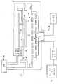
도 5는 본 발명에 따라 차후 금속화를 위해 일체식으로 구성된 CVD/PVD 시스템을 나타내는 도면;5 shows an CVD / PVD system integrally configured for subsequent metallization in accordance with the present invention;
도 6은 본 발명의 공정을 적절히 제어할 수 있는 컴퓨터 프로그램의 계층적 제어 구조를 나타내는 간략화된 블록도.6 is a simplified block diagram illustrating a hierarchical control structure of a computer program capable of appropriately controlling the process of the present invention.
*도면의 주요 부분에 대한 부호의 설명** Description of the symbols for the main parts of the drawings *
12 : 유전체층14 : 비아12
16 : 배리어/웨팅층 18 : 벽16 barrier /
22 : Al층24 : CVD/PVD 층22: Al layer 24: CVD / PVD layer
본 발명은 반도체 장치를 제조하기 위한 금속화 공정에 관한 것이다. 보다 상세하게는, 콘택 배리어층을 증착하는 방법에 관한 것이다.The present invention relates to a metallization process for manufacturing a semiconductor device. More specifically, it relates to a method of depositing a contact barrier layer.
서브-하프 미크론(sub-half micron)의 멀티레벨 금속화는 집적회로(IC)의 차세대 초고밀도 집적회로(VLSI)의 주요 기술중 하나로 대표된다. 콘택, 비아, 라인 및 트렌치를 포함하는 멀티레벨 상호접속부의 형상화된 구조물(feature)의 신뢰성 있는 형성은 VLSI의 성공 및 각각의 기판 및 다이 상에서 집적도를 증가시키기 위한 계속적인 노력에 있어 중요하다. 회로 밀도가 증가함에 따라, 형상화된 구조물(feature)의 폭은 0.50㎛ 이하로 감소되는 반면, 유전체층의 두께는 대체로 일정하게 유지되어, 형상화된 구조물의 어스펙트비, 즉 높이 대 폭이 증가하게 된다. 화학적 기상 증착(CVD) 및 물리적 기상 증착(PVD)과 같은 다양한 종래의 증착 공정은 기판상에 형성되는 형상화된 구조물의 어스펙트비가 2:1을 초과하는 경우, 특히 어스펙트비가 4:1에 이르는 경우에는 사용이 불가능하다.Multilevel metallization of sub-half microns is represented as one of the key technologies of the next generation ultra high density integrated circuit (VLSI) of integrated circuit (IC). Reliable formation of shaped features of multilevel interconnects, including contacts, vias, lines and trenches, is critical to the success of VLSI and ongoing efforts to increase the density on each substrate and die. As the circuit density increases, the width of the shaped features is reduced to 0.50 μm or less, while the thickness of the dielectric layer remains substantially constant, increasing the aspect ratio, ie height to width, of the shaped structures. . Various conventional deposition processes, such as chemical vapor deposition (CVD) and physical vapor deposition (PVD), have aspect ratios of more than 2: 1 for shaped structures formed on a substrate, especially when the aspect ratio reaches 4: 1. In this case, it is not available.
높은 어스펙트비의 형상화된 구조물 속에 금속을 함유한 균일한 층을 증착시키는 경우, 금속을 함유한 층이 형상화된 구조물의 측벽 상에 증착되어 형상화된 구조물을 완전히 채우기 전에 결국 형상화된 구조물 폭방향으로 집중되게 된다는 문제점이 있다. 부분적으로 채워진 형상화된 구조물이 커버되는 경우, 형상화된 구조물내에 증착된 물질 속에는 보이드 및 불연속성이 형성된다. 상기 보이드 및 불연속성은 신뢰성 없는 전기적 콘택, 상호접속부, 및 다른 회로의 형상화된 구조물을 야기할 수 있다.In the case of depositing a uniform layer containing metal in a high aspect ratio shaped structure, the metal containing layer is deposited on the sidewall of the shaped structure and eventually in the shape of the shaped structure width before it completely fills the shaped structure. There is a problem of concentration. When the partially filled shaped structure is covered, voids and discontinuities are formed in the material deposited in the shaped structure. The voids and discontinuities can lead to unreliable electrical contacts, interconnects, and shaped structures of other circuits.
형상화된 구조물에 형성되는 보이드를 감소시키는데 사용되는 방법 중 하나는 높은 온도(예를 들어, >350℃)에서 어닐링에 의해 금속을 평탄화시키는 것이다. 기판상에 연속하는 웨팅(wetting)층의 형성은 고온에서의 성공적인 평탄화에 있어 중요하다. 그러나 고온에서의 평탄화는 배리어/라이너(liner) 층들을 통해 주변 유전체 물질 속으로 금속의 확산을 야기시킬 수 있다. 결과적으로, 고온 공정은 기판의 콘택 레벨에서는 사용되지 않는다.One method used to reduce voids formed in shaped structures is to planarize the metal by annealing at high temperatures (eg,> 350 ° C). The formation of a continuous wetting layer on the substrate is important for successful planarization at high temperatures. However, planarization at high temperatures can cause diffusion of the metal through the barrier / liner layers into the surrounding dielectric material. As a result, high temperature processes are not used at the contact level of the substrate.
컨포멀한(conformal) 금속 박막이 차후의 물리적 기상 증착 및 저온(예를 들어, <550℃)에서 행해지는 평탄화 기술에 있어서 바람직한 웨팅층이란 것이 개시되어 있다. 이러한 공정은 Applied Materials, Inc. 에 양도된 "Low Temperature Integrated Metallization Process and Apparatus"란 제목으로, Mosely 등에 의해 1999년 3월 2일 발행된 미국 특허 5,877,087호에 보다 상세히 개시되어 있다.It is disclosed that a conformal metal thin film is a preferred wetting layer for subsequent physical vapor deposition and planarization techniques performed at low temperatures (eg, <550 ° C.). This process is performed by Applied Materials, Inc. US Patent No. 5,877,087, issued March 2, 1999 to Mosely et al., Entitled “Low Temperature Integrated Metallization Process and Apparatus”.
Mosely 등은 먼저 얇은 내화 금속층을 증착시킨 다음, 이어서 증착되는 PVD 금속을 위한 컨포멀한 웨팅층을 제공하기 위해 낮은 온도에서 CVD 금속층을 증착시키는 단계를 제시하였다. PVD 금속은 금속의 융점 온도 이하의 온도로 앞서 형성된 CVD 금속층 위에 증착된다. 형성되는 CVD/PVD 금속층은 대체로 형상화된 구조물에 보이드가 없다. 내화 금속층은 금속이 확산하기 쉬운 유전체층의 하부층 속으로 CVD 또는 PVD 금속층에 의한 확산에 대해 배리어로 제공된다. 전형적으로 내화 금속은 티타늄(Ti), 티타늄 질화물, 또는 이들 물질의 조합물과 같은 물질을 포함한다. CVD 및 PVD 층들은 종래에는 알루미늄(Al) 및 구리가 도핑된 알루미늄이었다. 그러나 하부 티타늄(Ti) 내화 금속층 위로 알루미늄의 증착은 티타늄 트리-알루미나이드(TiAl3) 형성에 문제를 나타낸다. Ti는 Al과 결합하여 절연체인 TiAl3를 형성하는 경향이 있어, 도전성 형상화된 구조물의 성능을 손상시킨다.Mosely et al. Proposed first depositing a thin refractory metal layer and then depositing a CVD metal layer at low temperature to provide a conformal wetting layer for the deposited PVD metal. PVD metal is deposited on the previously formed CVD metal layer at a temperature below the melting point temperature of the metal. The CVD / PVD metal layer formed is generally voids in the shaped structure. The refractory metal layer serves as a barrier against diffusion by the CVD or PVD metal layer into the underlying layer of the dielectric layer where the metal is likely to diffuse. Refractory metals typically include materials such as titanium (Ti), titanium nitride, or combinations of these materials. CVD and PVD layers were conventionally aluminum (Al) and copper doped aluminum. However, deposition of aluminum over the underlying titanium (Ti) refractory metal layer presents a problem for the formation of titanium tri-aluminate (TiAl3 ). Ti tends to combine with Al to form TiAl3 , an insulator, impairing the performance of conductive shaped structures.
TiAl3형성을 방지하기 위한 한가지 방법은 티타늄 질화물(TiN)층의 증착으로 Ti층의 증착을 행하는 것이다. 상부 TiN층은 Al과 결합되도록 사용가능한 Ti의 양을 감소시켜, TiAl3의 형성을 최소화시킨다. 추가로, TiN층은 티타늄과 알루미늄 모두와 양호한 결합을 제공하는 양호한 중간 "아교접착(glue)"층이나, 티타늄 질화물은 알루미늄과 상호작용하지는 않는다. Ti/TiN/Al의 시퀀스 증착은 TiAl3의 형성을 감소시키는 것으로 나타났지만, 상기 시퀀스는 Al과의 임의의 상호작용을 방지하기 위해 TiN층이 Ti층을 대부분 커버하도록 요구된다. 불행히도, 금속화 스택에서 추가적 층의 포함은 형상화된 구조물 사이즈를 더 감소시킨다. 금속화 스택의 두께를 최소화하기 위한 시도로, 매우 얇은층의 TiN층을 Ti층 상에 증착시킨다. 그러나 이러한 얇은 TiN층은 연속성이 적어 TiAl3의 형성을 방지하는데 덜 효과적이다.One way to prevent TiAl3 formation is to deposit a Ti layer by depositing a titanium nitride (TiN) layer. The upper TiN layer reduces the amount of Ti available to bond with Al, thereby minimizing the formation of TiAl3 . In addition, the TiN layer is a good intermediate "glue" layer that provides good bonding with both titanium and aluminum, but titanium nitride does not interact with aluminum. Although sequence deposition of Ti / TiN / Al has been shown to reduce the formation of TiAl3 , the sequence requires that the TiN layer cover most of the Ti layer to prevent any interaction with Al. Unfortunately, the inclusion of additional layers in the metallization stack further reduces the shaped structure size. In an attempt to minimize the thickness of the metallization stack, a very thin layer of TiN is deposited on the Ti layer. However, this thin TiN layer has less continuity and is less effective in preventing the formation of TiAl3 .
Ti/TiN 배리어층의 조합에 의해 배리어층 두께가 증가하는 것을 방지하는 또 다른 방법으로는 하부 Ti층이 없을 때 배리어층으로서 TiN을 사용하는 것이다. 그러나 TiN 배리어층은 작고, 높은 어스펙트비의 형상화된 구조물에서 덜 컨포멀한 배리어층을 형성할 수 있어, 증착되는 금속화 스택의 층들 사이에 확산을 방지하는데 비효과적일 수 있는 물리적 기상 증착에 의해 종래방식대로 증착된다.Another way to prevent the barrier layer thickness from increasing by a combination of Ti / TiN barrier layers is to use TiN as the barrier layer when there is no lower Ti layer. However, the TiN barrier layer can form a less conformal barrier layer in a small, high aspect ratio shaped structure, thereby preventing physical vapor deposition, which may be ineffective in preventing diffusion between the layers of the metallized stack being deposited. By the conventional method.
알루미늄 및 구리와 같은 전도성 금속에 대해 배리어층으로서 티타늄 및/또는 티타늄 질화물이 사용되는 다층 금속화 공정에서는 주목할만한 문제점이 발생한다. Mosely 등에 의해 개시된 평탄화 공정과 같은 고온(예를 들어 >350℃) 공정에서, 알루미늄은 Ti, Ti/TiN 또는 TiN 배리어층의 조합물로 확산될 수 있다. 금속이 콘택 레벨에 증착되는 경우, 전도성 금속은 배리어층으로 확산될 수 있고 하부 실리콘 및 주변 산화물들과 반응할 수 있다. 알루미늄 및 상기 알루미늄과 비교할 때 낮은 저항성, 높은 전자이동 저항성, 및 높은 전류 보유력으로 인해 사용되는 구리의 하부 실리콘 및 주변 산화물로의 확산은 인접한 층들의 전자 장치 특성 및 층들 사이의 전도성 경로를 변경시킬 수 있어, 전체 회로의 신뢰성을 감소시키고 장치 고장을 야기할 수 있는 단락 회로를 형성할 수 있다.A notable problem arises in multilayer metallization processes where titanium and / or titanium nitride are used as barrier layers for conductive metals such as aluminum and copper. In high temperature (eg> 350 ° C.) processes, such as the planarization process disclosed by Mosely et al., Aluminum may be diffused into a combination of Ti, Ti / TiN or TiN barrier layers. When the metal is deposited at the contact level, the conductive metal can diffuse into the barrier layer and react with the underlying silicon and surrounding oxides. Due to the low resistivity, high electromigration resistance, and high current retention compared to aluminum and aluminum, diffusion of copper into underlying silicon and surrounding oxides can alter the electronic device properties of the adjacent layers and the conductive paths between the layers. Thus, it is possible to form a short circuit that can reduce the reliability of the entire circuit and cause device failure.
따라서, 금속화 공정, 특히 높은 어스펙트비의 서브-하프 미크론의 콘택 및 알루미늄 및 구리와 같은 전도성 금속이 있는 비아를 채우고 평탄화시키는 공정에서는 신뢰성 있는 배리어층 설계안이 여전히 요구되고 있다.Thus, there is still a need for reliable barrier layer designs in metallization processes, particularly in the process of filling and planarizing high aspect ratio sub-half micron contacts and vias with conductive metals such as aluminum and copper.
본 발명의 실시예는 기판상에 전도성 형상화된 구조물을 형성하는 공정을 제공한다. 본 발명의 일면에서, 얇은 배리어층이 기판상에 형성되고 이어서 상기 배리어층 위로 화학적 기상 증착(CVD)에 의해 증착되는 얇고 컨포멀한 금속층이 형성된다. 배리어층은 두께가 약 2000Å 미만, 바람직하게는 약 5Å 내지 1000Å 사이이다. 컨포멀한 금속층은 두께가 약 200Å 내지 1미크론이며, 형상화된 구조물의 상부를 밀폐시키는 두께 미만의 두께가 바람직하다. 다음 금속층이 물리적 기상 증착에 의해 개구부를 거의 채울 수 있도록 약 660℃ 이하의 온도에서 컨포멀한 금속층 위로 증착된다. 다음 PVD 금속층과 컨포멀한 CVD 금속층이 약 250℃ 내지 약 450℃ 사이의 온도에서 어닐링 처리될 수 있다. 컨포멀한 CVD 금속층과 PVD 금속층은 일반적으로 금속 도체로, 바람직하게는 알루미늄(Al), 구리(Cu), 및 이들의 조합물이다. 배리어/웨팅층은 티타늄(Ta), 티타늄 질화물(TaNx), 텅스텐(W), 또는 텅스텐 질화물(WNx)의 그룹에서 선택된 물질 및 이들의 조합물로 구성된다. 바람직하게 공정은 통합된 공정 시스템에서 순차적으로 수행된다.Embodiments of the present invention provide a process for forming a conductive shaped structure on a substrate. In one aspect of the invention, a thin barrier layer is formed on a substrate and then a thin conformal metal layer is deposited over the barrier layer by chemical vapor deposition (CVD). The barrier layer has a thickness of less than about 2000 microns, preferably between about 5 microns and 1000 microns. The conformal metal layer has a thickness of about 200 kPa to 1 micron, preferably less than the thickness that seals the top of the shaped structure. The metal layer is then deposited over the conformal metal layer at a temperature of about 660 ° C. or less to substantially fill the opening by physical vapor deposition. The PVD metal layer and the conformal CVD metal layer may then be annealed at a temperature between about 250 ° C and about 450 ° C. The conformal CVD metal layer and the PVD metal layer are generally metal conductors, preferably aluminum (Al), copper (Cu), and combinations thereof. The barrier / wetting layer consists of a material selected from the group of titanium (Ta), titanium nitride (TaNx), tungsten (W), or tungsten nitride (WNx) and combinations thereof. Preferably the processes are performed sequentially in an integrated process system.
본 발명의 또 다른 면에서, 기판은 PVD 및 CVD 공정 챔버 모두를 포함하는 일체식 공정 시스템에서 행해지는 금속화 공정으로 생산된다. 기판은 반도체 기판, 상기 반도체 기판에 형성되며 내부에 개구부가 형성되며 반도체 기판과 연결되는 유전체층, 개구부의 표면 위에 형성되는 배리어/웨팅층을 포함하며, 배리어/웨팅층은 Ta, TaNx, W, WNx 그룹에서 선택된 물질, 및 이들의 조합물을 포함한다. 배리어층은 바람직하게는 약 2000Å 미만, 보다 바람직하게는 약 5Å 내지 1000Å의 두께를 갖는다. 다음, 화학적 기상 증착된 Al, Cu, 및 이들의 조합물과 같은 금속층이 배리어/웨팅층 상에 형성된다. 마지막으로, 화학적 기상 증착된 컨포멀한 금속층 위에 물리적 기상 증착 또는 전기도금에 의해 금속층이 증착된다. 물리적 기상 증착된 금속층은 약 400℃ 이하의 온도에서 증착되어 CVD 및 PVD 증착된 금속층이 개구부 속으로 흘러 그안에 보이드를 형성하지 않고 상호접속부를 형성할 수 있다. PVD 금속층은 바람직하게 Al, Cu 그룹에서 선택된 물질 및 이들의 조합물을 포함한다.In another aspect of the invention, the substrate is produced in a metallization process performed in an integrated process system including both PVD and CVD process chambers. The substrate includes a semiconductor substrate, a dielectric layer formed in the semiconductor substrate and having an opening formed therein, and a barrier / wetting layer formed on a surface of the opening, wherein the barrier / wetting layer includes Ta, TaNx, W, and WNx. Materials selected from the group, and combinations thereof. The barrier layer preferably has a thickness of less than about 2000 GPa, more preferably about 5 GPa to 1000 GPa. Next, metal layers such as chemical vapor deposited Al, Cu, and combinations thereof are formed on the barrier / wetting layer. Finally, the metal layer is deposited by physical vapor deposition or electroplating on the chemical vapor deposited conformal metal layer. The physical vapor deposited metal layer may be deposited at a temperature of about 400 ° C. or less such that the CVD and PVD deposited metal layers flow into the openings to form interconnects without forming voids therein. The PVD metal layer preferably comprises a material selected from Al, Cu groups and combinations thereof.
본 발명의 또 다른 면은 컴퓨터에 의해 판독되고 실행되는 경우, 챔버에서 플라즈마를 발생시키는 단계, 챔버에 위치된 타겟에 바이어스를 제공하는 단계, 코일에 바이어스를 제공하는 단계, 및 기판상에 물질을 증착하는 단계 동안 약 0.5mTorr 내지 약 100mTorr 사이의 챔버 압력을 유지하는 단계를 포함하는 프로그램 프로덕트를 제공한다. 프로그램 프로덕트는 약 200W 내지 약 24kW 사이의 RF 바이어스를 코일에 제공하며, 약 200W 내지 약 24kW 사이의 바이어스를 타겟에 제공한다. 프로그램 프로덕트는 약 0W 내지 1000W 사이의 바이어스를 기판에 제공하는 단계를 더 포함할 수 있다. 챔버에 위치된 타겟은 Ta, TaN, W, WN 그룹에서 선택된 물질 및 이들의 조합물이 바람직하다.Another aspect of the invention provides a method of generating plasma in a chamber, providing a bias to a target located in the chamber, providing a bias to a coil, and when performing a material on a substrate when read and executed by a computer. A program product comprising maintaining a chamber pressure between about 0.5 mTorr and about 100 mTorr during the deposition step. The program product provides an RF bias between about 200 W and about 24 kW to the coil and a bias between about 200 W and about 24 kW to the target. The program product may further comprise providing a bias between about 0W and 1000W to the substrate. The target located in the chamber is preferably a material selected from the group Ta, TaN, W, WN and combinations thereof.
이러한 방식으로 상기 열거된 본 발명의 특징, 장점 및 목적이 달성되며, 상기 내용을 간략히 요약한 본 발명의 상세한 설명을 참조로 이를 더욱더 이해할 수 있을 것이며, 첨부된 도면에 설명되는 실시예를 참조할 수 있다.In this way, the features, advantages, and objects of the invention enumerated above are achieved, and a more detailed understanding of the invention may be obtained by reference to the detailed description of the invention which is briefly summarized above, and with reference to the embodiments described in the accompanying drawings. Can be.
그러나 주목할 것은 첨부된 도면은 본 발명의 단지 전형적 실시예를 나타내는 것으로 본 발명의 범위를 한정하는 것은 아니며, 본 발명에 대해 동등한 다른 효과적인 실시예를 적용할 수 있다.It should be noted, however, that the appended drawings illustrate only typical embodiments of the invention and are not intended to limit the scope of the invention, and other equally effective embodiments may be applied to the invention.
일반적으로 본 발명은 낮은 공정 온도에서 증착될 수 있는 높은 어스펙트비의 서브-미크론 개구부의 개선된 비아 충전을 위한 효과적인 배리어층을 제공한다. 또한, 본 발명은 콘택, 비아, 라인 또는 다른 형상화된 구조물을 포함하는 높은 어스펙트비의 개구부를 약 660℃ 이하의 온도에서 금속화를 위한 방법을 제공한다. 특히, 본 발명은 바람직하게는 PVD 알루미늄(PVD Al) 또는 CVD 구리(CVD Cu)의 전도성 금속의 제 1 층, 및 바람직하게는 PVD 알루미늄(PVD Al) 또는 PVD 구리(PVD Cu)의 전도성 금속의 제 2 층을 적용하여 높은 어스펙트비의 개구부를 충진시키기 위한 개선된 스텝 커버리지를 제공한다. 얇은 CVD층은 유전체층의 디웨팅(dewetting) 또는 CVD 및/또는 PVD 금속층 보다 융점이 크고 절연체 보다 CVD 금속층 사용으로 유전체를 사용하는 것보다 큰 웨팅을 제공하는 전도성 금속이 포함된 얇은 배리어/웨팅층의 증착에 의해 유전체층으로의 확산을 방지한다. 탄탈(Ta), 티타늄 질화물(TaNx), 텅스텐(W), 텅스텐 질화물(WNx), 및 이들의 조합물과 같은 배리어층은 인접한 유전체 물질 속으로 알루미늄 또는 구리의 확산을 방지하는데 바람직하다.In general, the present invention provides an effective barrier layer for improved via filling of high aspect ratio sub-micron openings that can be deposited at low process temperatures. The present invention also provides a method for metallization of high aspect ratio openings, including contacts, vias, lines or other shaped structures, at temperatures below about 660 ° C. In particular, the invention preferably comprises a first layer of conductive metal of PVD aluminum (PVD Al) or CVD copper (CVD Cu), and preferably of a conductive metal of PVD aluminum (PVD Al) or PVD copper (PVD Cu). The second layer is applied to provide improved step coverage for filling high aspect ratio openings. The thin CVD layer is a thin barrier / wetting layer containing a conductive metal that provides a dewetting of the dielectric layer or a wetting point greater than that of the CVD and / or PVD metal layer and provides a wetting greater than the use of the dielectric by using the CVD metal layer over the insulator. Deposition is prevented by diffusion into the dielectric layer. Barrier layers such as tantalum (Ta), titanium nitride (TaNx), tungsten (W), tungsten nitride (WNx), and combinations thereof are desirable to prevent the diffusion of aluminum or copper into adjacent dielectric materials.
도 1은 상부에 패턴화된 유전체층(12)이 형성되고 내부에 비아(14)가 형성된 기판(10)의 개략도이다. 탄탈 또는 탄탈 질화물과 같은 물질의 얇은 배리어/웨팅층(16)이 비아(14)의 벽(18)과 바닥 레벨(20)을 포함하는 유전체층(12)의 표면 전체를 거의 커버하는 기판상에 일정하게 증착된다. 일반적으로 얇은 탄탈층(16)은 약 2000Å 미만의 두께, 바람직하게는 약 5Å 내지 약 1000Å 사이, 보다더 바람직하게는 약 100Å 내지 약 400Å 사이의 두께를 갖는다. 컨포멀한 CVD Al층(22)은 콘택 또는 비아의 상부를 브리지(bridge) 또는 밀폐시키는 두께를 초과하지 않는 두께로 일반적으로는 약 2000Å 내지 약 1미크론, 바람직하게는 하프-미크론 형상화된 구조물에 대해 약 2000Å 미만의 두께로 배리어/웨팅층(16) 상에 증착된다. 컨포멀한 CVD Al 층(22)은 시드층, 또는 차후 증착되는 금속층에 대한 웨팅층으로서 작용한다.1 is a schematic diagram of a
도 2는 상부에 PVD층(23)을 형성하기 위해 CVD Al 또는 Cu층(22) 위로 증착되는 PVD Al 또는 Cu층을 나타내는 기판(10)의 개략도이다. 혼합된 CVD/PVD층(24)은 PVD층이 CVD층 위로 증착되어 CVD층과 합쳐져 생성될 수 있다. 혼합된 층(24)의 상부표면(26)은 대체로 평탄하다. PVD층은 일정 도판트를 함유할 수 있고 증착에 따라 PVD 물질이 CVD 물질과 혼합될 수 있어 도판트가 PVD/CVD 혼합층(24)을 곳곳에 분산될 수 있다. 도판트는 알루미늄층 내의 구리일 수 있고, 구리층 내의 알루미늄 또는 주석(Sn)일 수 있다.2 is a schematic diagram of a
배리어/웨팅층은 CVD층에 양호한 웨팅을 제공하기 때문에, PVD 증착 동안 기판 온도는 알루미늄의 융점(660℃)을 초과하는 것을 요구하지 않으며, 약 660℃ 이하의 온도에서 행해질 수 있고 바람직하게는 약 400℃ 이하 온도에서 행해진다. 낮은 금속화 공정 온도는 금속층과 배리어층 사이에서 압출성형(extrusion) 및 확산 문제를 적게 야기시키는 공정의 금속층에서 스트레스를 적게 나타낸다. 또한, 개선된 배리어층은 유전체층과 하부 기판 속으로 금속층으로 인한 잠재적인 확산을 최소화시키는 확산에 대해 높은 열 안정성 및 고저항을 제공한다.Since the barrier / wetting layer provides good wetting for the CVD layer, the substrate temperature during PVD deposition does not require exceeding the melting point of aluminum (660 ° C.), and can be done at temperatures of about 660 ° C. or less and preferably about It is performed at 400 degrees C or less temperature. Low metallization process temperatures result in less stress in the metal layer of the process which results in less extrusion and diffusion problems between the metal layer and the barrier layer. In addition, the improved barrier layer provides high thermal stability and high resistance to diffusion that minimizes potential diffusion due to the metal layer into the dielectric layer and the underlying substrate.
바람직하게, 금속화 공정은 CVD 및 PVD 공정 챔버 모두를 포함하고 있는 일체식 공정 시스템에서 행해진다. 일단 기판이 진공 분위기 속으로 도입되면, 증착 단계들 사이에서 산화층을 형성하지 않고 비아 및 콘택의 금속화가 행해진다. 이는 기판이 CVD 및 PVD 증착층의 증착을 거치기 위해 하나의 공정 시스템으로부터 또 다른 시스템으로 전송될 필요가 없기 때문이다. 따라서, 연속 배리어/CVD/PVD는 산화를 방지한다는 장점을 제공하며, 기판상에 형성된 형상화된 구조물들의 전기 저항성을 증가시키는 산화물을 형성하지 않고 단계들 사이에 공기 중에 노출될 수 있다.Preferably, the metallization process is done in an integrated process system that includes both CVD and PVD process chambers. Once the substrate is introduced into a vacuum atmosphere, metallization of vias and contacts is performed without forming an oxide layer between deposition steps. This is because the substrate does not need to be transferred from one process system to another to undergo deposition of CVD and PVD deposition layers. Thus, continuous barrier / CVD / PVD offers the advantage of preventing oxidation and can be exposed to air between steps without forming oxides that increase the electrical resistance of shaped structures formed on the substrate.
본 발명의 평탄화 및 비아 충진 공정은 바람직하게 표면 장력의 효과로 인해 각각의 융점 이하 온도에서 흐를 수 있다고 입증된 알루미늄 및 구리를 혼합한다. 이들의 낮은 융점 및 흐름 특성으로 인해, Al 및 Cu는 고온에서 하부 유전체층에 양호한 커버리지 또는 점착성을 갖지 않는다. Al 및 Cu는 금속의 웨팅 및 커버리지를 개선시키기 위해 사용되는 종래의 티타늄(Ti) 및 티타늄 질화물(TiN) 배리어/웨팅층을 통해 확산될 수 있다. 따라서, 본 발명은 개선된 평탄화 및 비아 충진을 위하여 Al 및 Cu의 흐름 특성을 바람직하게 사용하기 위해 확산에 대해 높은 열적 안정성 및 저항성을 갖는 배리어/웨팅층을 확산으로 혼합한다.The planarization and via filling processes of the present invention preferably mix aluminum and copper which have proven to flow at temperatures below their respective melting points due to the effect of surface tension. Due to their low melting point and flow characteristics, Al and Cu do not have good coverage or adhesion to the underlying dielectric layer at high temperatures. Al and Cu can be diffused through conventional titanium (Ti) and titanium nitride (TiN) barrier / wetting layers used to improve the wetting and coverage of the metal. Accordingly, the present invention mixes diffusion barrier / wetting layers with high thermal stability and resistance to diffusion in order to preferably use the flow properties of Al and Cu for improved planarization and via filling.
확산에 대해 높은 열적 안정성 및 저항성을 갖는 양호하고 컨포멀한 커버리지를 갖는 바람직한 배리어/웨팅층은 탄탈(Ta), 탄탈 질화물(TaNx), 텅스텐(W), 텅스텐 질화물(WNx), 또는 이들의 조합물을 포함한다. 알루미늄 및 구리와 함께 양호한 점착성을 갖고, 약 2985℃의 융점 온도를 갖는 탄탈(Ta), 및 약 3400℃의 융점 온도를 갖는 텅스텐(W)이 배리어/웨팅 물질로 바람직하며 이는 이들이 알루미늄 또는 구리보다 융점이 높고 열적 안정성이 높기 때문이다. Ta 및 W는 질산 탄탈 질화물(TaNx) 및 텅스텐 질화물(WNx)로서 또한 증착될 수 있으며, 질산층은 Ta 및 W 위로 개선된 확산 및 웨팅 특성을 가질 수 있다.Preferred barrier / wetting layers with good and conformal coverage with high thermal stability and resistance to diffusion are tantalum (Ta), tantalum nitride (TaNx), tungsten (W), tungsten nitride (WNx), or combinations thereof. Contains water. Tantalum (Ta) having good adhesion with aluminum and copper, having a melting point temperature of about 2985 ° C., and tungsten (W) having a melting point temperature of about 3400 ° C. are preferred as barrier / wetting materials, which are more preferred than aluminum or copper. This is because the melting point is high and the thermal stability is high. Ta and W may also be deposited as tantalum nitrate (TaNx) and tungsten nitride (WNx), and the nitrate layer may have improved diffusion and wetting properties over Ta and W.
배리어/웨팅층들은 화학적 기상 증착(CVD), 물리적 기상 증착(PVD), 또는 이온화된 금속 플라즈마(IMP) PVD로 공지된 고/중간 밀도 플라즈마 CVD에 의해 증착될 수 있다. 배리어/웨팅 물질은 약 2000Å 미만의 두께, 바람직하게는 약 5Å 내지 약 1000Å 사이, 보다더 바람직하게는 약 100Å 내지 약 400Å 사이로 증착된다. 배리어/웨팅층의 증착은 패턴화된 유전체층 위로 연속적인 막을 형성하도록 높은 어스펙트비의 형상화된 구조물 표면상에 얇고 컨포멀한 막을 증착할 수 있는, 이온화 금속 플라즈마(IMP) 증착 기술에 의해 행해지는 것이 바람직하다. W 및 WNx 층 또한 높은 어스펙트비의 형상화된 구조물에서 컨포멀한 막을 제공하는 IMP PVD에 의해 증착될 수 있다. 본 발명의 배리어 물질의 사용은 Ti/TiN 배리어층 구성이 1-단계 증착 공정을 요구함에 따라 개별 웨팅층을 증착시킬 필요성을 제거하여 기판 처리량을 증가시킨다.Barrier / wetting layers may be deposited by high / medium density plasma CVD known as chemical vapor deposition (CVD), physical vapor deposition (PVD), or ionized metal plasma (IMP) PVD. The barrier / wetting material is deposited to a thickness of less than about 2000 microns, preferably between about 5 microns and about 1000 microns, even more preferably between about 100 microns and about 400 microns. Deposition of the barrier / wetting layer is performed by an ionized metal plasma (IMP) deposition technique that can deposit a thin, conformal film on a high aspect ratio shaped structure surface to form a continuous film over a patterned dielectric layer. It is preferable. W and WNx layers may also be deposited by IMP PVD, which provides a conformal film in high aspect ratio shaped structures. The use of the barrier material of the present invention increases substrate throughput by eliminating the need to deposit individual wetting layers as the Ti / TiN barrier layer configuration requires a one-step deposition process.
도 3은 IMP 챔버(40)의 개략적 단면도이다. IMP VectraTM 챔버로 공지된 IMP 공정 챔버는 캘리포니아 산타 클라라의 Applied Material, Inc.에서 시판한다. 또한, IMP 챔버는 Applied Material, Inc. 에서 시판하는 EnduraTM 플랫폼에 포함될 수 있다. IMP 공정은 스퍼터된 물질이 통과됨에 따라 스퍼터된 타겟 물질의 이온화를 야기시키는 표준 PVD 공정보다 고압력의 플라즈마, 고밀도 플라즈마(HDP)를 제공한다. HDP-PVD 이온화는 높은 어스펙트비의 형상화된 구조물에서도 층을 컨포멀하게 증착시키고 바이어스된 기판 표면에 거의 직교하는 방향으로 스퍼터된 물질들이 부착되도록 한다. 챔버(40)는 측벽(101), 리드(102), 및 바닥부(103)를 포함한다. 리드(102)는 증착되는 물질의 타겟(105)을 지지하는 타겟 후면판(104)을 포함한다. 타겟(105)은 바람직하게 증착되는 전도성 물질, 보다 바람직하게는 탄탈 및 탈탈에 대한 텅스텐, 탄탈 질화물, 텅스텐 및 텅스텐 질화물 증착물로 구성된다.3 is a schematic cross-sectional view of the
챔버(40) 내의 개구부(108)는 챔버(40)에 대해 챔버로 기판(10)을 전송하고 회수할 수 있는 로봇(도시되지 않음)의 액서스를 제공하며, 기판(10)은 챔버(40)에 수용되고 기판 지지체(112) 상에 위치된다. 기판 지지체(112)는 챔버에 스퍼터되는 물질층을 증착시키기 위해 기판(10)을 지지하며 일반적으로 접지된다. 기판 지지체(112)는 상기 기판 지지체(112)를 높이고 낮추는 리프트 모터(114)에 장착되며, 기판(10)이 그 위에 배치된다. 리프트 모터(118)에 연결된 리프트 플레이트(116)가 챔버(40)에 장착되고 기판 지지체(112)에 장착된 핀(120a, 120b)을 상승 및 하강시킨다. 핀(120a, 120b)은 기판 지지체(112)의 표면에서 표면으로 기판(10)을 상승시키고 하강시킨다.Opening 108 in
코일(122)이 기판 지지체(112)와 타겟(105) 사이에 장착되고 타겟(105)과 기판(10) 사이에 플라즈마를 발생시키고 유지하는 것을 돕기 위해 챔버(40)에 유도 결합된 자계를 제공한다. 코일(122)은 타겟과 기판(10) 사이의 위치로 인해 스퍼터되며 바람직하게는 타겟(105)과 유사한 구성물로 구성된다. 예를 들어, 코일(122)은 구리 및 인으로 구성될 수 있다. 코일(122)의 도핑 퍼센트는 원하는 층 조성물에 따라 타겟 도핑 퍼센트와 비교되어 변경될 수 있고 관련 도핑 퍼센트를 변화시킴으로써 실험적으로 결정된다. 코일(122)에 공급되는 전력은 스퍼터되는 물질을 이온화시키는 플라즈마의 밀도를 높인다. 다음 이온화된 물질은 기판(10)을 향하게 되어 기판상에 증착된다.A
차폐물(124)이 스퍼터되는 물질로부터 챔버 측벽(101)을 차폐시키기 위해 챔버(40)에 위치된다. 또한, 차폐물(124)은 코일 지지체(126)에 의해 코일(122)을 지지한다. 코일 지지체(126)는 차폐물(124)과 챔버(40)로부터 코일(122)을 전기적으로 절연시키며 코일과 유사한 물질로 구성될 수 있다. 클램프 링(128)이 코일(122)과 기판 지지체(112) 사이에 장착되어 기판(10)이 클램프 링(128)의 하부와 결합되도록 공정 위치로 상승되는 경우, 스퍼터되는 물질로부터 기판의 외부 엣지 및 후방을 차폐한다. 소정의 챔버 구성에서는, 차폐물(124)은 기판이 전송될 수 있도록 차폐물(124) 아래로 하강되는 경우 클램프 링(128)을 지지한다.A
이러한 형태의 스퍼터링 챔버에 3개의 전원 장치가 사용된다. 전원 장치(130)는 타겟(105)에 바람직한 DC 전력을 인가하여 처리 가스가 플라즈마를 형성하도록 야기시키며, 또한 RF 전력이 사용될 수 있다. 타겟 후면판(104) 뒤에 배치된 자석(106a, 106b)은 자석(105)에 인접한 전자 밀도를 증가시켜, 타겟에서의 이온화를 증가시켜 스퍼터링 효율을 증가시키게 된다. 자석(106a, 106b)은 타겟 면과 일반적으로 평행한 자계 라인을 발생시켜, 타겟 부근의 전자는 스퍼터링을 위한 가스 원자의 이온화 및 충돌 가능성을 증가시켜 스피닝 궤도에 트랩된다. 전원 장치(132), 바람직하게 RF 전원 장치가 플라즈마 밀도를 증가시키기 위해 코일(122)에 전력을 공급한다. 또 다른 전원 장치(134), 전형적으로는 DC 전원 장치는 플라즈마와 관련하여 기판 지지체(112)를 바이어스시켜 기판(10)을 향해 이온화되어 스퍼터된 물질의 방향성 흡인력을 제공한다.Three power supplies are used for this type of sputtering chamber. The
아르곤 또는 헬륨과 같은 불활성 가스 또는 질소와 같은 반응성 가스의 처리 가스는 각각 질량 흐름 제어기(142,144)에 의해 측정됨에 따라 가스 소스(138,140)로부터 가스 인입구(136)를 통해 챔버(40)로 공급된다. 진공 펌프(146)는 챔버(40)를 배기시켜 챔버(40)에 원하는 압력을 유지하기 위해 배기 포트(148)에서 챔버(40)와 연결된다.Process gas of an inert gas such as argon or helium or a reactive gas such as nitrogen is supplied from the
일반적으로 제어기(141)는 전원 장치들, 리프트 모터, 가스 주입을 위한 질량 흐름 제어기, 진공 펌프의 기능 및 다른 챔버와 관련된 부품 기능을 제어한다. 제어기(141)는 처리 가스가 플라즈마를 형성하고 타겟 물질을 스퍼터링하도록 타겟(105)에 연결된 전원 장치(130)를 제어한다. 또한, 제어기(141)는 플라즈마 밀도를 증가시키고 스퍼터된 물질을 이온화시키기 위해 코일(122)에 연결된 전원 장치(132)를 제어한다. 또한, 제어기(141)는 기판 표면에서 이온화되고 스퍼터된 물질의 방향성 흡입력을 제공하도록 전원 장치(134)를 제어한다. 제어기(141)는 바람직한 실시예에서는 하드 디스크 드라이브인 메모리에 저장된 시스템 제어 소프트웨어를 실행시키며, 아날로그 및 디지털 입력/출력 보드, 인터페이스 보드, 및 스텝퍼 모터 제어기 보드(도시되지 않음)를 포함할 수 있다. 일반적으로 광학 및/또는 자석 센서(도시되지 않음)가 이동식 기계 어셈블리의 위치를 이동시키고 결정하기 위해 사용된다.
탄탈, 탄탈 질화물, 텅스텐, 및 텅스텐 질화물의 IMP 증착을 위한 예시적 공정 단계는 캘리포니아 산타 클라라의 Applied Materials, Inc. 에서 시판하는 IMP VectraTM챔버로 공지된 이온 금속 플라즈마(IMP) 챔버에서 200mm 웨이퍼에 대해 행해진다. 헬륨 또는 아르곤과 같은 불활성 가스가 약 0.5 mTorr 내지 약 100 mTorr, 보다 바람직하게는 약 20 mTorr 내지 약 50 mTorr의 챔버 압력을 생성하기 위해 충분한 비율로 챔버에 주입된다. 200mm 기판에 대해, 지지 부재에 공급되는 전력 레벨은 타겟 및 코일에서의 전력이 약 0W 내지 500W, 바람직하게는 약 1kW 내지 약 3kW가 바람직하며 보다 바람직하게는 기판 전력은 약 300W이다. 기판 지지체의 전력 밀도는 바람직하게 약 0.5W/㎠ 내지 약 1.6W/㎠이며, 보다 바람직하게는 1.0W/㎠이다. 300mm 기판에 대해, 지지 부재에 공급되는 전력 레벨은 바람직하게 약 500W 내지 1000W이고 보다 바람직하게는 750W이고 전력 밀도는 약 0.7W/㎠ 내지 1.4W/㎠, 보다 바람직하게는 약 1.0W/㎠이다. IMP-PVD 챔버에서의 타겟은 약 200 와트(W) 내지 약 24 킬로와트(kW) 및 약 20V 내지 약 2400V로 DC-바이어스되고, 바람직하게 DC-바이어스는 약 1kW 내지 약 3kW 사이 및 약 100V 내지 약 300V사이이다. 바람직하게 코일은 200W 내지 약 24kW 사이, 보다 바람직하게는 약 1kW 내지 약 3kW 사이로 RF-바이어스된다.Exemplary process steps for IMP deposition of tantalum, tantalum nitride, tungsten, and tungsten nitride are described in Applied Materials, Inc., Santa Clara, California. On an 200 mm wafer in an ion metal plasma (IMP) chamber known as the IMP Vectra™ chamber available from. An inert gas such as helium or argon is injected into the chamber at a sufficient rate to produce a chamber pressure of about 0.5 mTorr to about 100 mTorr, more preferably about 20 mTorr to about 50 mTorr. For 200 mm substrates, the power level supplied to the support member is preferably between about 0 W and 500 W, preferably between about 1 kW and about 3 kW, with power at the target and coil being more preferably about 300 W. The power density of the substrate support is preferably about 0.5 W / cm 2 to about 1.6 W / cm 2, more preferably 1.0 W / cm 2. For 300 mm substrates, the power level supplied to the support member is preferably about 500 W to 1000 W, more preferably 750 W and a power density of about 0.7 W / cm 2 to 1.4 W / cm 2, more preferably about 1.0 W / cm 2. . The target in the IMP-PVD chamber is DC-biased from about 200 watts (W) to about 24 kilowatts (kW) and from about 20 V to about 2400 V, preferably the DC-bias is between about 1 kW to about 3 kW and from about 100 V to about Between 300V. Preferably the coil is RF-biased between 200W and about 24kW, more preferably between about 1kW and about 3kW.
기판은 약 10℃ 내지 약 400℃ 사이의 온도, 바람직하게는 약 300℃ 이하로 유지된다. 탄탈 질화물 또는 텅스텐 질화물과 같은 질산화 배리어막의 증착을 위해서, 일반적으로 처리 가스는 아르곤과 같은 불활성 가스 및 질소와 같은 질산화 가스를 포함하며, 아르곤은 탄탈 또는 텅스텐 타겟에 충격을 가하는 플라즈마 이온을 위한 주요 가스 소스로서의 기능을 하며 질소는 기판상에 증착되는 탄탈 또는 텅스텐 질화막을 형성하기 위해 타겟으로부터 스퍼터된 원자(텅스텐)와 반응한다.The substrate is maintained at a temperature between about 10 ° C and about 400 ° C, preferably about 300 ° C or less. For the deposition of nitridation barrier films such as tantalum nitride or tungsten nitride, the process gas generally includes an inert gas such as argon and a nitric oxide gas such as nitrogen, and argon is the primary gas for plasma ions that impact the tantalum or tungsten targets. It functions as a source and nitrogen reacts with atoms sputtered from the target (tungsten) to form a tantalum or tungsten nitride film deposited on the substrate.
다음 CVD Al, Cu층, 또는 다른 전도성 금속이 비아의 상부를 교락시키지(bridging) 않고 비아 구조상에 컨포멀한 웨팅층을 형성하기 위해 배리어층 상에 증착된다. CVD Al 및 Cu는 그 위에 차후 증착되는 PVD Al 또는 Cu층의 수용을 위해 배리어/웨팅층 위로 컨포멀한 웨팅층을 제공한다. 부가적으로, 전기도금 및/또는 무전해(electroless) 증착과 같은 전기화학적 증착 공정이 웨팅층 위로 전도성층을 증착시키는데 사용될 수 있다.A CVD Al, Cu layer, or other conductive metal is then deposited on the barrier layer to form a conformal wetting layer on the via structure without bridging the top of the via. CVD Al and Cu provide a conformal wetting layer over the barrier / wetting layer for receipt of PVD Al or Cu layers subsequently deposited thereon. Additionally, electrochemical deposition processes such as electroplating and / or electroless deposition can be used to deposit conductive layers over the wetting layer.
CVD Al 또는 Cu는 다양한 조건하에서 증착될 수 있으나, 전형적인 공정은 약 180℃ 내지 약 265℃ 사이의 기판 온도 및 약 20Å/sec 내지 약 130Å/sec 사이의 증착비를 필요로 한다. 바람직하게, 화학 기상 증착된 컨포멀한 금속층은 약 200Å 내지 약 1 미크론 사이의 두께를 갖으나, 형상화된 구조물, 특히 서브-미크론의 높은 어스펙트 비를 갖는 형상화된 구조물 상부를 밀폐시키는 두께 미만의 두께를 갖는 것이 더 바람직하다. CVD Al 또는 Cu 증착은 약 1 mTorr 내지 약 80 mTorr 사이의 챔버 압력에서 행해질 수 있고, 보다 바람직하게 챔버 압력은 약 25 Torr이다.CVD Al or Cu may be deposited under a variety of conditions, but typical processes require a substrate temperature between about 180 ° C. and about 265 ° C. and a deposition ratio between about 20 μs / sec and about 130 μs / sec. Preferably, the chemical vapor deposited conformal metal layer has a thickness of between about 200 microns and about 1 micron, but less than a thickness that closes the top of the shaped structure, particularly the shaped structure with a high aspect ratio of sub-micron. It is more preferred to have a thickness. CVD Al or Cu deposition may be performed at a chamber pressure between about 1 mTorr and about 80 mTorr, more preferably the chamber pressure is about 25 Torr.
CVD Al은 종래의 CVD 공정에 의해 증착될 수 있으나, CVD Al을 위한 바람직한 증착 반응은 수소 가스(H2)와 디메틸 알루미늄 수소화물(DMAH)의 반응을 필요로 한다. CVD Cu층은 공지된 임의의 CVD Cu 공정 또는 Cu+2(hfac)2 및 Cu+2(fod)2(fod는 헵타플로오르 디메틸 옥탄디에네(heptafluoro dimethyl octanediene)의 약자이다)를 포함하는 전구체 가스에 의해 증착될 수 있으나, 바람직한 공정은 캐리어 가스로서 아르곤과 함께 휘발성 액체 복합물 Cu+1hfac, TMVS(hfac는 헥사플로오르 아세틸아세토네이트 음이온(hexafluoro acetylacetonate anion)의 약자이고 TMVS는 트리메틸비닐실란(trimethylvinylsilane)의 약자이다)를 사용한다. 상기 복합물은 대기 중에서 액체이기 때문에, 현재 반도체 제조에서 사용되는 표준 CVD 버블러 전조 배송 시스템에서 활용될 수 있다. TMVS 및 Cu+2(hfac)2 모두는 챔버로부터 배기되는 증착 반응의 휘발성 부산물이다. 휘발성 액체 복합물 Cu+1hfac, TMVS는 바람직하게 열 보조 공정으로, 열 또는 플라즈마 보조 공정을 통해 Cu를 증착하는데 사용된다. 플라즈마 강화 공정에서의 기판 온도는 바람직하게 약 100 내지 약 400℃인 반면, 열 공정에는 약 50 내지 약 300℃ 사이, 더 바람직하게는 약 170℃이다. 바람직하게는, 화학적 기상 증착된 컨포멀한 금속층은 약 200Å 내지 약 1 미크론 사이의 두께를 갖는다. 가장 바람직하게 화학적 기상 증착된 컨포멀한 금속층은 비아 또는 콘택, 특히 서브-미크론 형상화된 구조물에서 상부를 밀폐시키는 두께를 초과하지 않는 두께를 갖는다.CVD Al can be deposited by conventional CVD processes, but the preferred deposition reaction for CVD Al requires the reaction of hydrogen gas (H2 ) with dimethyl aluminum hydride (DMAH). The CVD Cu layer can be any known CVD Cu process or precursor comprising Cu+2 (hfac)2 and Cu+2 (fod)2 (fod stands for heptafluoro dimethyl octanediene). The preferred process is volatile liquid complex Cu+1 hfac, TMVS (hfac stands for hexafluoro acetylacetonate anion and TMVS is trimethylvinylsilane) with argon as carrier gas. trimethylvinylsilane). Since the composite is a liquid in the atmosphere, it can be utilized in standard CVD bubbler precursor delivery systems currently used in semiconductor manufacturing. Both TMVS and Cu+2 (hfac)2 are volatile by-products of the deposition reaction exiting the chamber. Volatile liquid composite Cu+1 hfac, TMVS is preferably used for the deposition of Cu via a heat or plasma assisted process, as a heat assisted process. The substrate temperature in the plasma intensification process is preferably about 100 to about 400 ° C., while the thermal process is between about 50 to about 300 ° C., more preferably about 170 ° C. Preferably, the chemical vapor deposited conformal metal layer has a thickness between about 200 microns and about 1 micron. Most preferably the chemical vapor deposited conformal metal layer has a thickness that does not exceed the thickness that encloses the top in vias or contacts, especially sub-micron shaped structures.
도 4는 본 발명의 CVD 증착 공정을 수행하기에 적합한 CVD 증착 챔버(38)의 개략적 부분 단면도이다. CVD 증착 챔버(38)는 주변 측벽(62) 및 실링(64)을 포함한다. 챔버(38)는 챔버속으로 운반되는 처리 가스를 분사시키기 위한 처리 가스 분배기(66)를 포함한다. 질량 흐름 제어기 및 기상 동작 밸브는 증착 챔버(38)속으로 처리 가스의 흐름을 제어하는데 사용된다. 가스 분배기(66)는 전형적으로 기판(10) 위에 또는 기판(10) 주변 부근에 장착된다. 지지 부재(68)는 증착 챔버(38)에서 기판을 지지하도록 제공된다. 기판은 챔버(38)의 측벽(62)에 있는 기판 로딩 인입구를 통해 챔버(38) 속으로 주입되어 지지체(68) 상에 위치된다. 지지체(68)는 지지 리프트 벨로즈(bellows)(70)에 의해 상승되거나 하강될 수 있어 기판과 가스 배분기(66) 사이의 갭이 조절된다. 지지체(68)에서의 홀을 통해 삽입되는 리프트 핑거를 포함하는 리프트 핑거 어셈블리(72)는 챔버(38) 안팎으로 기판의 전송을 용이하게 하기 위해 지지체 위로 기판을 상승 및 하강시키는데 사용될 수 있다. 다음 가열 히터(74)가 챔버에 제공되어 기판을 신속히 가열시킨다. 기판의 신속한 가열 및 냉각 공정은 생산량을 증가시키고, 동일 챔버내에서 상이한 온도에서 동작하는 연속적인 공정 사이에서 신속한 사이클링을 허용하는데 바람직하다. 일반적으로 기판(10) 온도는 지지체(68)의 온도로부터 짐작된다.4 is a schematic partial cross-sectional view of a
기판은 수평한 구멍난 배리어 플레이트(78) 위의 공정 영역(76)에서 처리된다. 배리어 플레이트(78)는 챔버(38)로부터 소모되는 처리 가스를 배기시키기 위한 배기 시스템(82)과 유체적으로 연통되는 배기 홀(80)을 포함한다. 전형적인 배기 시스템(82)은 약 10 mTorr의 최소 진공을 달성할 수 있는 회전 베인(vane) 진공 펌프(도시되지 않음)를 포함하며, 부산물 가스를 세정하기 위한 세정 시스템을 선택적으로 포함한다. 챔버(38)에서의 압력은 기판의 측면에서 감지되며 배기 시스템(82)에서의 트로틀 밸브를 조절함으로써 조절된다.The substrate is processed in the
플라즈마 발생기(84)는 플라즈마 강화 화학적 기상 증착 공정을 위한 챔버(38)의 공정 영역(95)에서 플라즈마를 발생시키기 위해 제공된다. 플라즈마 발생기(84)는 (i) 증착 챔버를 둘러싸는 인덕터 코일(도시되지 않음)에 유도적으로 RF 전류를 인가함으로써, (ii) 챔버에서 처리 전극에 용량적으로 RF 전류를 인가함으로써, 또는 (iii) 유도적으로 용량적으로 챔버벽 또는 다른 전극을 접지시킴으로써 플라즈마를 발생시킬 수 있다. DC 또는 RF는 공정 영역(76)에서 플라즈마를 발생시키기 위해 증착 챔버 속으로 유도 결합 에너지로 인덕터 코일(도시되지 않음)에 인가될 수 있다. RF 전류가 사용되는 경우, RF 전류 주파수는 약 400KHZ 내지 16MHZ이고, 보다 바람직하게는 13.56MHZ이다. 선택적으로, 알루미늄 산화물 또는 석영으로 구성된 가스 차단 또는 플라즈마 포커스 링(도시되지 않음)이 처리 가스 또는 기판 주변의 플라즈마 흐름을 견제하는데 사용될 수 있다.
기판상에 CVD Al 또는 Cu 웨팅층의 증착이 이루어지고, 기판은 CVD 및 PVD 금속층의 융점 온도 이하의 온도에서 PVD Al 또는 Cu 층이 증착되는 PVD 챔버로 전송된다. PVD Al층은 약 660℃ 이하의 기판 온도로 증착되고; PVD Cu층은 약 550℃ 이하의 기판 온도로 증착된다. 바람직하게, PVD Al층 및 Cu층은 약 400℃ 이하의 기판 온도로 증착된다. 금속층은 알루미늄에 대해서는 약 400℃에서 그리고 구리에 대해서는 약 200℃에서 PVD 증착 공정 동안 고형 금속층으로서 견고히 적소에 남아있는 배리어/웨팅층에 흐름이 시작된다. 본 발명의 탄탈 및 다른 배리어/웨팅 조성물이 양호한 웨팅 특성을 갖고 있기 때문에, CVD 금속은 약 400℃에서의 디웨팅을 방지한다. 따라서, 탄탈과 같은 배리어/웨팅층의 증착은 알루미늄 또는 구리가 배리어층으로 확산될 가능성을 감소시키는 알루미늄 및 구리의 융점 이하 온도에서 금속층의 평탄화를 달성할 수 있다.Deposition of a CVD Al or Cu wetting layer is performed on the substrate, and the substrate is transferred to a PVD chamber where the PVD Al or Cu layer is deposited at a temperature below the melting temperature of the CVD and PVD metal layers. The PVD Al layer is deposited at a substrate temperature of about 660 ° C. or less; The PVD Cu layer is deposited at a substrate temperature of about 550 ° C. or less. Preferably, the PVD Al layer and the Cu layer are deposited at a substrate temperature of about 400 ° C. or less. The metal layer begins to flow to the barrier / wetting layer which remains firmly in place as the solid metal layer during the PVD deposition process at about 400 ° C. for aluminum and at about 200 ° C. for copper. Since tantalum and other barrier / wetting compositions of the present invention have good wetting properties, CVD metals prevent dewetting at about 400 ° C. Thus, deposition of a barrier / wetting layer, such as tantalum, can achieve planarization of the metal layer at temperatures below the melting point of aluminum and copper, reducing the likelihood of aluminum or copper diffusion into the barrier layer.
기판 개구부의 금속화를 위한 본 발명의 방법은 기판 표면을 예비세정하는 단계, 스퍼터된 원자가 이온화되는 고밀도 플라즈마의 IMP PVD 공정, 또는 조준된 PVD 공정을 사용하여 탄탈 또는 탄탈 질화물과 같은 배리어층을 증착하는 단계, CVD 공정을 사용하여 배리어층 위로 전도성 금속을 증착하는 단계, PVD 금속층 및 CVD 금속층이 차후 개구부를 채우도록 약 660℃ 이하의 온도에서 스퍼터링 챔버에서 PVD 금속을 증착하는 순차적인 단계를 포함한다. 선택적으로, 형성된 금속화 스택은 금속화 스택 표면의 반사성을 감소시키기 위해 PVD TiN 비반사 코팅("ARC")의 증착과 같은 또 다른 처리를 거쳐 금속화 스택의 포토리소그라픽 성능을 개선시킬 수 있다. 추가로, 스택은 화학적 기계적 연마(CMP)에 의해 처리될 수 있다.The method of the present invention for metallization of substrate openings deposits a barrier layer such as tantalum or tantalum nitride using a preliminary cleaning of the substrate surface, an IMP PVD process of a high density plasma in which sputtered atoms are ionized, or an aimed PVD process. Depositing a conductive metal over the barrier layer using a CVD process, and sequential depositing the PVD metal in the sputtering chamber at a temperature of about 660 ° C. or less such that the PVD metal layer and the CVD metal layer subsequently fill the openings. . Optionally, the formed metallized stack may be subjected to another treatment, such as the deposition of a PVD TiN antireflective coating (“ARC”), to improve the photolithographic performance of the metallized stack to reduce the reflectivity of the metallized stack surface. . In addition, the stack can be processed by chemical mechanical polishing (CMP).
본 발명의 공정은 PVD 및 CVD 챔버 모두를 갖는 멀티챔버 공정 장치 또는 클러스터 툴에서 행해지는 것이 바람직하지만, 공정들은 그와 연결된 PVD 또는 CVD 챔버를 갖는 개별 시스템에서 행해질 수도 있다. 본 발명의 CVD 및 PVD 공정을 수행하기에 적합한 멀티챔버 공정 장치(35)의 개략을 도 5에 도시하였다. 장치는 캘리포니아 산타 클라라 Applied Materials, Inc. 에서 상업적으로 시판하는 ENDURAⓡ이다. 유사한 스테이지 진공 기판 처리 시스템이 본 명세서에서 참조로하는 1993년 2월 16일 공개된, Tepman 등에 의해 "Staged-Vacuum Substrate Processing System and Method"란 제목의 미국 특허 5,186,718에 개시되어 있다. 본 명세서에서 도시된 장치의 특정 실시예는 반도체 기판과 같은 평면형 기판을 처리하는데 적합하며, 본 발명에서는 도시를 위해 제공된 것으로, 발명의 범주내에서 사용되는 것은 아니다.Although the process of the present invention is preferably performed in a multichamber process apparatus or cluster tool having both PVD and CVD chambers, the processes may be performed in a separate system having a PVD or CVD chamber connected thereto. A schematic of a
장치(35)는 스퍼터링과 같은 PVD 공정을 수행하기 위해 적어도 1개의 밀폐된 PVD 증착 챔버(36)를 포함하는 상호접속부된 공정 챔버의 클러스터를 포함한다. PVD 챔버(36)는 기판을 면하는 스퍼터링 물질의 스퍼터링 타겟을 포함한다. 타겟은 챔버와 전기적으로 절연되고 스퍼터링 플라즈마를 생성하기 위한 처리 전극으로서의 역할을 한다. 스퍼터링 공정 동안, 아르곤 또는 크세논과 같은 스퍼터링 가스가 챔버(36) 속으로 주입된다. DC 바이어스가 스퍼터링 타겟에 인가되고, 챔버에 배치된 기판 지지 부재는 전기적으로 접지된다. 챔버(36)에서의 전계는 기판상에 물질을 증착시키는 타겟을 스퍼터링하는 스퍼터링 플라즈마를 형성하기 위해 스퍼터링 가스를 이온화시킨다. 스퍼터링 공정에서, 플라즈마는 스퍼터링 타겟에 약 100 내지 20,000 와트, 바람직하게는 약 100 내지 약 10,000와트의 전력 레벨의 DC 또는 RF 전압을 인가함으로써 발생된다.
본 발명에 있어, 장치(35)는 바람직하게 컨포멀한 PVD Al 또는 Cu층을 증착하기 위한 PVD 챔버(36) 및 CVD Al 또는 Cu층을 증착하기 위한 CVD 챔버(38)를 포함한다. 장치(35)는 IMP PVD 챔버(40) 또는 탄탈/탄탈 질화물(Ta/TaN)과 같은 본 발명의 배리어층을 증착하기 위한 또다른 배리어/웨팅층 챔버, 금속화 스택의 포토리소그라픽 성능을 개선시키는 금속화 스택의 반사성을 감소시키는 TiN 비반사 코팅(ARC)층을 증착하기 위한 PVD TiN ARC 챔버(41), 오염물을 제거하기 위한 2개의 예비세정 챔버(42)(Applied Materials에서 시판하는 예비세정 Ⅱ 챔버), 2개의 디가스(degas) 챔버(44), 및 2개의 로드록 챔버(46)를 포함한다. 장치(35)는 전송 로봇(49,51)을 포함하는 2개의 전송 챔버(48,50), 및 전송 챔버(48,50)를 분리시키는 2개의 쿨다운 챔버(52)를 포함한다. 장치(35)는 컴퓨터 프로그래 프로덕트(141)로 마이크로프로세서 제어기(54)를 프로그래밍함으로써 자동화 처리된다. 그러나 공정은 각각의 챔버, 또는 상기 챔버의 조합에 의해 작동될 수 있다.In the present invention, the
제어 시스템Control system
도 6을 참조로, 본 발명의 공정은 캘리포니아, Synenergy Microsystems에서 상업적으로 시판하는, 예로 68400 마이크로프로세서와 같은 주변 제어 부품을 갖춘 메모리 시스템에 포함되는 중앙 처리 장치(CPU)를 포함하는 종래의 컴퓨터 시스템에서 구동되는 컴퓨터 프로그램 프로덕트(141)를 사용하여 행해질 수 있다. 컴퓨터 프로그램 코드는 예를 들어 68000 어셈블리 언어, C, C++ 또는 파스칼과 같은 종래의 컴퓨터 판독가능 프로그래밍 언어로 기록될 수 있다. 적절한 프로그램 코드는 종래의 텍스트 에디터를 사용하여 단일 파일, 또는 다중 파일로 기록되고, 컴퓨터의 메모리 시스템과 같은 컴퓨터 유저블 미디엄에 저장 또는 기재된다. 기록된 코드 텍스트가 하이 레벨 언어인 경우, 코드는 컴파일되어, 컴파일러 코드가 예비컴파일된 윈도우 라이브러리 루틴의 목표 코드와 링크된다. 링크되어 컴파일된 목적 코드를 실행시키기 위해서, 시스템 사용자는 목적 코드를 불러내어 컴퓨터 시스템은 메모리에서 코드를 로드시키게 되어 CPU를 판독하고 프로그램에서 인식되는 업무를 수행하기 위해 코드를 실행시킨다.Referring to FIG. 6, a process of the present invention includes a conventional computer system including a central processing unit (CPU) included in a memory system with peripheral control components such as a 68400 microprocessor, commercially available from Synenergy Microsystems, California. It can be done using a
도 6은 컴퓨터 프로그램(141)의 계층적인 제어 구조의 블록도를 나타낸다. 사용자는 공정 선택기 서브루틴(142) 속에 공정 세트 및 공정 챔버수를 기록한다. 공정 세트는 특정 공정 챔버에서 특정 공정을 실행하기 위해 필요한 공정 파라미터의 세트를 미리결정하여 예정된 세트의 수에 의해 식별된다. 공정 파라미터는 예를 들어, 공정 가스 조성 및 유속, 온도, 압력, 냉각 가스 압력과 같은 플라즈마 조건, 및 챔버 벽 온도와 같은 공정 조건에 관한 것이다.6 shows a block diagram of a hierarchical control structure of
공정 시퀀서 서브루틴(143)은 식별된 공정 챔버 및 공정 선택 서브루틴(142)으로부터 공정 파라미터의 세트를 수용하고, 다양한 공정 챔버의 동작을 제어하는 프로그램 코드를 포함한다. 멀티 사용자는 공정 세트 수와 공정 챔버 수를 기록하거나, 또는 멀티 공정 세트 수와 공정 챔버 수를 기록할 수 있어, 시퀀서 서브루틴(143)이 원하는 시퀀스에서 선택된 공정을 예정할 수 있도록 동작한다. 바람직하게 시퀀서 서브루틴(143)은, (i) 챔버가 사용되는 경우를 결정하기 위해 공정 챔버의 작동을 모니터링하는 단계, (ii) 사용되는 챔버에서 어떤 공정이 행해지는지를 결정하는 단계, (iii) 공정 챔버의 유용성 및 실행되는 공정 타입에 근거하여 원하는 공정을 실행하는 단계를 수행하도록 하는 프로그램 코드를 포함한다. 공정 챔버를 모니터링하는 종래의 방법으로 풀링(polling)이 사용될 수 있다. 실행될 공정이 예정되면, 시퀀서 서브루틴(143)은 선택된 공정을 위한 원하는 공정 조건, 또는 각각 특정 사용자 기록 요청의 "에이지(age)" 또는 우선순위를 계획하여 결정하도록 포함되는 것이 바람직한 시스템 프로그래머와 관련한 다른 요인과 비교하여 사용되는 공정 챔버의 현재 조건을 고려하도록 설계할 수 있다.
일단 시퀀서 서브루틴(143)이 다음에 실행될 공정 챔버 및 공정 세트 조합을 결정되면, 시퀀서 서브루틴(143)은 시퀀서 서브루틴(143)에 의해 결정된 공정 세트에 따라 상이한 공정 챔버에서 다수의 공정 업무를 제어하는 챔버 매니저 서브루틴(114A-C)에 특정 공정 세트 파라미터를 통과시킴으로써 공정 세트를 실행시킨다. 예를 들어, 챔버 매니저 서브루틴(144A)은 개시된 공정 챔버(38)내에서 CVD 공정 작업을 제어하기 위한 프로그램 코드를 포함한다. 또한 챔버 매니저 서브루틴(144)은 다양한 챔버 컴포넌트 서브루틴 또는 프로그램 코드 모듈의 실행을 제어하며, 챔버 컴포넌트의 동작 제어는 선택된 공정 세트를 실행하는 데 있어 요구된다. 챔버 컴포넌트 서브루틴 예로는 기판 위치결정 서브루틴(145), 처리 가스 제어 서브루틴(146), 압력 제어 서브루틴(147), 히터 제어 서브루틴(148), 및 플라즈마 제어 서브루틴(149)이 있다.Once the
동작시에, 챔버 매니저 서브루틴(144A)은 실행되는 특정 공정 세트 따라 공정 컴포넌트 서브루틴을 선택적으로 예정하거나 호출한다. 챔버 매니저 서브루틴(144A)은 시퀀서 서브루틴(143)이 다음에 실행되는 공정 챔버 및 공정 세트를 예정하는 방법과 유사하게 공정 컴포넌트 서브루틴을 예정한다. 일반적으로, 챔버 매니저 서브루틴(144A)은 다양한 챔버 요소를 모니터링하는 단계, 실행되는 공정 세트를 위한 공정 파라미터에 기초하여 동작하는데 요구되는 부품을 결정하는 단계, 및 상기 모니터링 및 결정 단계에 대응하여 챔버 컴포넌트 서브루틴을 실행시키는 단계를 포함한다.In operation,
가정 예(Hypothetical Example)Hypothetical Example
이하 가정되는 예는 기판상의 콘택 레벨에서 형상화된 구조물을 형성하는 방법을 설명한다. 탄탈 질화물층은 형상화된 구조물의 알루미늄 충전을 위한 배리어층으로 사용된다.The hypothesized example below describes a method of forming a shaped structure at a contact level on a substrate. Tantalum nitride layers are used as barrier layers for aluminum filling of shaped structures.
기판상에 하프-미크론의 형상화된 구조물는 이하의 본 발명에 의해 채워질 수 있다. 하프-미크론 형상화된 구조물을 포함하는 기판 표면은 임의의 산화물 또는 다른 오염물을 포함하는 약 100Å 내지 400Å의 물질을 제거하기 위해 예비세정된다. 그 다음 기판은 탄탈 타겟을 갖는 IMP-PVD TaN 챔버에 위치되며, 아르곤 및 질소를 포함하는 플라즈마가 부딪쳐 기판상에 약 400Å의 컨포멀한 탄탈 질화물층이 증착된다. 그 다음 기판은 CVD 챔버로 전송되며 약 1500Å의 컨포멀한 알루미늄층이 배리어층에 증착된다. 다음 기판은 350℃ 이하에서 약 4000Å의 벌크형(bulk) 알루미늄을 증착시키기 위해 알루미늄 타겟을 갖는 PVD Al 챔버로 전송된다. 알루미늄층(컨포멀하고 커다란)이 어닐링 챔버에서 가열처리된다. 어닐링 동안 기판 온도는 약 450℃ 이하로 유지된다.The half-micron shaped structure on the substrate can be filled by the following invention. The substrate surface comprising the half-micron shaped structure is precleaned to remove material between about 100 kV and 400 kV including any oxides or other contaminants. The substrate is then placed in an IMP-PVD TaN chamber with a tantalum target, where a plasma containing argon and nitrogen strikes to deposit a layer of conformal tantalum nitride on the substrate. The substrate is then transferred to a CVD chamber and a conformal aluminum layer of about 1500 microns is deposited on the barrier layer. The substrate is then transferred to a PVD Al chamber with an aluminum target to deposit about 4000 mm of bulk aluminum below 350 ° C. An aluminum layer (conformal and large) is heated in the annealing chamber. The substrate temperature is maintained below about 450 ° C. during the annealing.
본 발명의 실시예에 관해 설명되어있으나, 발명의 또 다른 실시예들을 본 발명의 기본 범주에서 이탈하지 않고 고안할 수 있다. 본 발명의 범주는 이하 청구항으로 한정된다.While embodiments of the invention have been described, other embodiments of the invention can be devised without departing from the basic scope of the invention. The scope of the invention is defined by the claims below.
본 발명은 낮은 온도에서 특히 기판상의 특정한 콘택 레벨의 높은 어스펙트비의 미크론 이하 개구부에서 개선된 비아 충진을 위한 효과적인 배리어층을 제공한다.The present invention provides an effective barrier layer for improved via filling at low temperatures, especially at high aspect ratio sub-micron openings at specific contact levels on a substrate.
Claims (41)
Translated fromKoreanApplications Claiming Priority (2)
| Application Number | Priority Date | Filing Date | Title |
|---|---|---|---|
| US09/425,082US6207558B1 (en) | 1999-10-21 | 1999-10-21 | Barrier applications for aluminum planarization |
| US09/425,082 | 1999-10-21 |
Publications (2)
| Publication Number | Publication Date |
|---|---|
| KR20010040149A KR20010040149A (en) | 2001-05-15 |
| KR100743330B1true KR100743330B1 (en) | 2007-07-26 |
Family
ID=23685069
Family Applications (1)
| Application Number | Title | Priority Date | Filing Date |
|---|---|---|---|
| KR1020000062088AExpired - Fee RelatedKR100743330B1 (en) | 1999-10-21 | 2000-10-21 | Barrier applications for aluminum planarization |
Country Status (6)
| Country | Link |
|---|---|
| US (2) | US6207558B1 (en) |
| EP (1) | EP1094503A3 (en) |
| JP (1) | JP2001237314A (en) |
| KR (1) | KR100743330B1 (en) |
| SG (1) | SG92749A1 (en) |
| TW (1) | TW526583B (en) |
Families Citing this family (55)
| Publication number | Priority date | Publication date | Assignee | Title |
|---|---|---|---|---|
| US6429120B1 (en)* | 2000-01-18 | 2002-08-06 | Micron Technology, Inc. | Methods and apparatus for making integrated-circuit wiring from copper, silver, gold, and other metals |
| JP3351383B2 (en)* | 1999-04-21 | 2002-11-25 | 日本電気株式会社 | Method for manufacturing semiconductor device |
| JP2001057359A (en)* | 1999-08-17 | 2001-02-27 | Tokyo Electron Ltd | Plasma processing device |
| KR100338112B1 (en)* | 1999-12-22 | 2002-05-24 | 박종섭 | Method of forming a copper wiring in a semiconductor device |
| KR100330163B1 (en)* | 2000-01-06 | 2002-03-28 | 윤종용 | A Method of Forming Tungsten Contact Plug in A Semiconductor Devices |
| US7211512B1 (en)* | 2000-01-18 | 2007-05-01 | Micron Technology, Inc. | Selective electroless-plated copper metallization |
| US7262130B1 (en)* | 2000-01-18 | 2007-08-28 | Micron Technology, Inc. | Methods for making integrated-circuit wiring from copper, silver, gold, and other metals |
| US6420262B1 (en)* | 2000-01-18 | 2002-07-16 | Micron Technology, Inc. | Structures and methods to enhance copper metallization |
| US6376370B1 (en) | 2000-01-18 | 2002-04-23 | Micron Technology, Inc. | Process for providing seed layers for using aluminum, copper, gold and silver metallurgy process for providing seed layers for using aluminum, copper, gold and silver metallurgy |
| US6528180B1 (en) | 2000-05-23 | 2003-03-04 | Applied Materials, Inc. | Liner materials |
| US6342448B1 (en)* | 2000-05-31 | 2002-01-29 | Taiwan Semiconductor Manufacturing Company | Method of fabricating barrier adhesion to low-k dielectric layers in a copper damascene process |
| US6674167B1 (en)* | 2000-05-31 | 2004-01-06 | Micron Technology, Inc. | Multilevel copper interconnect with double passivation |
| US6423629B1 (en)* | 2000-05-31 | 2002-07-23 | Kie Y. Ahn | Multilevel copper interconnects with low-k dielectrics and air gaps |
| US6511912B1 (en)* | 2000-08-22 | 2003-01-28 | Micron Technology, Inc. | Method of forming a non-conformal layer over and exposing a trench |
| TW512180B (en)* | 2000-09-21 | 2002-12-01 | Promos Technologies Inc | Method for maintaining the cleanness of a vacuum chamber of physical vapor deposition system |
| US6486064B1 (en)* | 2000-09-26 | 2002-11-26 | Lsi Logic Corporation | Shallow junction formation |
| US7172497B2 (en)* | 2001-01-05 | 2007-02-06 | Asm Nutool, Inc. | Fabrication of semiconductor interconnect structures |
| US6953392B2 (en)* | 2001-01-05 | 2005-10-11 | Asm Nutool, Inc. | Integrated system for processing semiconductor wafers |
| US20040259348A1 (en)* | 2001-02-27 | 2004-12-23 | Basol Bulent M. | Method of reducing post-CMP defectivity |
| TWI222154B (en)* | 2001-02-27 | 2004-10-11 | Asm Nutool Inc | Integrated system for processing semiconductor wafers |
| US20020192948A1 (en)* | 2001-06-15 | 2002-12-19 | Applied Materials, Inc. | Integrated barrier layer structure for copper contact level metallization |
| US20030008243A1 (en)* | 2001-07-09 | 2003-01-09 | Micron Technology, Inc. | Copper electroless deposition technology for ULSI metalization |
| US20040089421A1 (en)* | 2002-02-15 | 2004-05-13 | Komandur Srinivasan M. | Distributed control system for semiconductor manufacturing equipment |
| US6736929B2 (en)* | 2002-02-15 | 2004-05-18 | Nutool, Inc. | Distributed control system for semiconductor manufacturing equipment |
| JP2003318395A (en)* | 2002-04-19 | 2003-11-07 | Hitachi Ltd | Method for manufacturing semiconductor device |
| US6716733B2 (en)* | 2002-06-11 | 2004-04-06 | Applied Materials, Inc. | CVD-PVD deposition process |
| US6846380B2 (en)* | 2002-06-13 | 2005-01-25 | The Boc Group, Inc. | Substrate processing apparatus and related systems and methods |
| US6803309B2 (en)* | 2002-07-03 | 2004-10-12 | Taiwan Semiconductor Manufacturing Co., Ltd | Method for depositing an adhesion/barrier layer to improve adhesion and contact resistance |
| KR100460066B1 (en)* | 2002-07-19 | 2004-12-04 | 주식회사 하이닉스반도체 | Method for fabricating semiconductor device |
| US7138719B2 (en)* | 2002-08-29 | 2006-11-21 | Micron Technology, Inc. | Trench interconnect structure and formation method |
| KR100457843B1 (en)* | 2002-09-18 | 2004-11-18 | 삼성전자주식회사 | Method for forming a contact |
| KR100480632B1 (en)* | 2002-11-16 | 2005-03-31 | 삼성전자주식회사 | Method for forming metal wiring layer of semiconductor device |
| US6977217B1 (en) | 2002-12-03 | 2005-12-20 | Cypress Semiconductor Corporation | Aluminum-filled via structure with barrier layer |
| US6794753B2 (en)* | 2002-12-27 | 2004-09-21 | Lexmark International, Inc. | Diffusion barrier and method therefor |
| US20040214417A1 (en)* | 2003-03-11 | 2004-10-28 | Paul Rich | Methods of forming tungsten or tungsten containing films |
| CN100352011C (en)* | 2003-03-25 | 2007-11-28 | 富士通株式会社 | Semiconductor device manufacturing equipment and semiconductor device manufacturing method |
| US20040221959A1 (en)* | 2003-05-09 | 2004-11-11 | Applied Materials, Inc. | Anodized substrate support |
| US8372205B2 (en)* | 2003-05-09 | 2013-02-12 | Applied Materials, Inc. | Reducing electrostatic charge by roughening the susceptor |
| US7220665B2 (en) | 2003-08-05 | 2007-05-22 | Micron Technology, Inc. | H2 plasma treatment |
| KR100583637B1 (en)* | 2003-08-19 | 2006-05-26 | 삼성전자주식회사 | Tungsten Contact Forming Method and Tungsten Contact Forming Equipment in Semiconductor Devices |
| JPWO2005055298A1 (en)* | 2003-12-03 | 2007-08-23 | 東京エレクトロン株式会社 | Plasma processing apparatus and multi-chamber system |
| US7180193B2 (en)* | 2004-04-13 | 2007-02-20 | Taiwan Semiconductor Manufacturing Company, Ltd. | Via recess in underlying conductive line |
| US7323230B2 (en)* | 2004-08-02 | 2008-01-29 | Applied Materials, Inc. | Coating for aluminum component |
| US7732056B2 (en) | 2005-01-18 | 2010-06-08 | Applied Materials, Inc. | Corrosion-resistant aluminum component having multi-layer coating |
| US7550055B2 (en)* | 2005-05-31 | 2009-06-23 | Applied Materials, Inc. | Elastomer bonding of large area sputtering target |
| US20070012557A1 (en)* | 2005-07-13 | 2007-01-18 | Applied Materials, Inc | Low voltage sputtering for large area substrates |
| US8173228B2 (en)* | 2006-01-27 | 2012-05-08 | Applied Materials, Inc. | Particle reduction on surfaces of chemical vapor deposition processing apparatus |
| KR100764739B1 (en)* | 2006-05-10 | 2007-10-08 | 삼성전자주식회사 | Method of forming a semiconductor device |
| DE102007035837A1 (en)* | 2007-07-31 | 2009-02-05 | Advanced Micro Devices, Inc., Sunnyvale | Semiconductor device with a grain orientation layer |
| JP5651298B2 (en)* | 2008-10-24 | 2015-01-07 | シチズン時計マニュファクチャリング株式会社 | Plasma-assisted reactive thin film forming apparatus and thin film forming method using the same |
| US9269615B2 (en)* | 2012-07-20 | 2016-02-23 | Globalfoundries Inc. | Multi-layer barrier layer for interconnect structure |
| US8728931B2 (en)* | 2012-07-20 | 2014-05-20 | GlobalFoundries, Inc. | Multi-layer barrier layer for interconnect structure |
| US8772158B2 (en) | 2012-07-20 | 2014-07-08 | Globalfoundries Inc. | Multi-layer barrier layer stacks for interconnect structures |
| US8623758B1 (en) | 2012-10-22 | 2014-01-07 | Globalfoundries Inc. | Subtractive metal multi-layer barrier layer for interconnect structure |
| CN105112976A (en)* | 2015-07-31 | 2015-12-02 | 深圳市星火辉煌系统工程有限公司 | Surface micro-arc modification process for CVD tool |
Citations (1)
| Publication number | Priority date | Publication date | Assignee | Title |
|---|---|---|---|---|
| KR19990023960A (en)* | 1997-08-29 | 1999-03-25 | 야스카와 히데아키 | Semiconductor device and manufacturing method thereof |
Family Cites Families (60)
| Publication number | Priority date | Publication date | Assignee | Title |
|---|---|---|---|---|
| DE374591C (en)* | 1921-05-29 | 1923-04-28 | Gersham Bowmar | Piston with a vacuum chamber arranged in the cavity of the piston body |
| US5259881A (en) | 1991-05-17 | 1993-11-09 | Materials Research Corporation | Wafer processing cluster tool batch preheating and degassing apparatus |
| US5010032A (en) | 1985-05-01 | 1991-04-23 | Texas Instruments Incorporated | Process for making CMOS device with both P+ and N+ gates including refractory metal silicide and nitride interconnects |
| JPS639925A (en) | 1986-06-30 | 1988-01-16 | Nec Corp | Manufacture of semiconductor device |
| JPS6373660A (en) | 1986-09-17 | 1988-04-04 | Fujitsu Ltd | Semiconductor device |
| US4951601A (en) | 1986-12-19 | 1990-08-28 | Applied Materials, Inc. | Multi-chamber integrated process system |
| JPS63176031A (en) | 1987-01-16 | 1988-07-20 | Stanley Electric Co Ltd | optical communication equipment |
| FR2610142B1 (en) | 1987-01-23 | 1989-05-26 | Lami Philippe | METHOD FOR FORMING METALLIC PASSAGE HOLES OF UNEQUAL HEIGHTS |
| US4960732A (en) | 1987-02-19 | 1990-10-02 | Advanced Micro Devices, Inc. | Contact plug and interconnect employing a barrier lining and a backfilled conductor material |
| US4784973A (en) | 1987-08-24 | 1988-11-15 | Inmos Corporation | Semiconductor contact silicide/nitride process with control for silicide thickness |
| US4926237A (en) | 1988-04-04 | 1990-05-15 | Motorola, Inc. | Device metallization, device and method |
| US4994410A (en) | 1988-04-04 | 1991-02-19 | Motorola, Inc. | Method for device metallization by forming a contact plug and interconnect using a silicide/nitride process |
| US4938996A (en) | 1988-04-12 | 1990-07-03 | Ziv Alan R | Via filling by selective laser chemical vapor deposition |
| FR2634317A1 (en) | 1988-07-12 | 1990-01-19 | Philips Nv | METHOD FOR MANUFACTURING SEMICONDUCTOR DEVICE HAVING AT LEAST ONE CONTACT LEVEL THROUGH SMALL DIMENSION CONTACT OPENINGS |
| JPH0226051A (en) | 1988-07-14 | 1990-01-29 | Seiko Epson Corp | Manufacture of semiconductor device |
| US4920072A (en) | 1988-10-31 | 1990-04-24 | Texas Instruments Incorporated | Method of forming metal interconnects |
| US4920073A (en) | 1989-05-11 | 1990-04-24 | Texas Instruments, Incorporated | Selective silicidation process using a titanium nitride protective layer |
| US5186718A (en) | 1989-05-19 | 1993-02-16 | Applied Materials, Inc. | Staged-vacuum wafer processing system and method |
| US5102827A (en) | 1989-05-31 | 1992-04-07 | At&T Bell Laboratories | Contact metallization of semiconductor integrated-circuit devices |
| JPH038359A (en) | 1989-06-06 | 1991-01-16 | Fujitsu Ltd | Manufacturing method of semiconductor device |
| US5240505A (en) | 1989-08-03 | 1993-08-31 | Mitsubishi Denki Kabushiki Kaisha | Method of an apparatus for forming thin film for semiconductor device |
| US5028565A (en) | 1989-08-25 | 1991-07-02 | Applied Materials, Inc. | Process for CVD deposition of tungsten layer on semiconductor wafer |
| ATE137357T1 (en) | 1989-09-26 | 1996-05-15 | Canon Kk | METHOD FOR PRODUCING A DEPOSITED LAYER USING ALKYLALUMINUM HYDRIDE AND METHOD FOR PRODUCING A SEMICONDUCTOR COMPONENT |
| JPH0727880B2 (en) | 1989-11-10 | 1995-03-29 | 株式会社東芝 | Method for manufacturing semiconductor device |
| US5043299B1 (en) | 1989-12-01 | 1997-02-25 | Applied Materials Inc | Process for selective deposition of tungsten on semiconductor wafer |
| US5478780A (en) | 1990-03-30 | 1995-12-26 | Siemens Aktiengesellschaft | Method and apparatus for producing conductive layers or structures for VLSI circuits |
| US5043300A (en) | 1990-04-16 | 1991-08-27 | Applied Materials, Inc. | Single anneal step process for forming titanium silicide on semiconductor wafer |
| JP2513900B2 (en) | 1990-05-08 | 1996-07-03 | 富士通株式会社 | Method for manufacturing semiconductor device |
| US5091339A (en) | 1990-07-23 | 1992-02-25 | Microelectronics And Computer Technology Corporation | Trenching techniques for forming vias and channels in multilayer electrical interconnects |
| US5023201A (en) | 1990-08-30 | 1991-06-11 | Cornell Research Foundation, Inc. | Selective deposition of tungsten on TiSi2 |
| US5080933A (en) | 1990-09-04 | 1992-01-14 | Motorola, Inc. | Selective deposition of polycrystalline silicon |
| US5032233A (en) | 1990-09-05 | 1991-07-16 | Micron Technology, Inc. | Method for improving step coverage of a metallization layer on an integrated circuit by use of a high melting point metal as an anti-reflective coating during laser planarization |
| US5250465A (en) | 1991-01-28 | 1993-10-05 | Fujitsu Limited | Method of manufacturing semiconductor devices |
| US5143867A (en) | 1991-02-13 | 1992-09-01 | International Business Machines Corporation | Method for depositing interconnection metallurgy using low temperature alloy processes |
| US5147819A (en) | 1991-02-21 | 1992-09-15 | Micron Technology, Inc. | Semiconductor metallization method |
| US5250467A (en) | 1991-03-29 | 1993-10-05 | Applied Materials, Inc. | Method for forming low resistance and low defect density tungsten contacts to silicon semiconductor wafer |
| JP2533414B2 (en) | 1991-04-09 | 1996-09-11 | 三菱電機株式会社 | Wiring connection structure of semiconductor integrated circuit device and manufacturing method thereof |
| US5292558A (en) | 1991-08-08 | 1994-03-08 | University Of Texas At Austin, Texas | Process for metal deposition for microelectronic interconnections |
| DE69226411T2 (en) | 1991-09-30 | 1998-12-24 | At & T Corp., New York, N.Y. | Manufacture of a conductive area in electronic devices |
| US5312774A (en) | 1991-12-05 | 1994-05-17 | Sharp Kabushiki Kaisha | Method for manufacturing a semiconductor device comprising titanium |
| US5300813A (en) | 1992-02-26 | 1994-04-05 | International Business Machines Corporation | Refractory metal capped low resistivity metal conductor lines and vias |
| US5371042A (en) | 1992-06-16 | 1994-12-06 | Applied Materials, Inc. | Method of filling contacts in semiconductor devices |
| US5240739A (en) | 1992-08-07 | 1993-08-31 | Micron Technology | Chemical vapor deposition technique for depositing titanium silicide on semiconductor wafers |
| CA2082771C (en) | 1992-11-12 | 1998-02-10 | Vu Quoc Ho | Method for forming interconnect structures for integrated circuits |
| JPH0722339A (en) | 1993-07-05 | 1995-01-24 | Toshiba Corp | Thin film formation method |
| US5427666A (en) | 1993-09-09 | 1995-06-27 | Applied Materials, Inc. | Method for in-situ cleaning a Ti target in a Ti + TiN coating process |
| US5384284A (en) | 1993-10-01 | 1995-01-24 | Micron Semiconductor, Inc. | Method to form a low resistant bond pad interconnect |
| US5585308A (en) | 1993-12-23 | 1996-12-17 | Sgs-Thomson Microelectronics, Inc. | Method for improved pre-metal planarization |
| US5439731A (en) | 1994-03-11 | 1995-08-08 | Cornell Research Goundation, Inc. | Interconnect structures containing blocked segments to minimize stress migration and electromigration damage |
| JP3400078B2 (en) | 1994-04-13 | 2003-04-28 | 富士写真フイルム株式会社 | Image reading device |
| JPH0810693A (en) | 1994-06-30 | 1996-01-16 | Dainippon Screen Mfg Co Ltd | Drying of resist film and device thereof |
| US5534462A (en) | 1995-02-24 | 1996-07-09 | Motorola, Inc. | Method for forming a plug and semiconductor device having the same |
| US5877087A (en)* | 1995-11-21 | 1999-03-02 | Applied Materials, Inc. | Low temperature integrated metallization process and apparatus |
| JPH1064902A (en) | 1996-07-12 | 1998-03-06 | Applied Materials Inc | Aluminum film forming method and film forming apparatus |
| US6001420A (en) | 1996-09-23 | 1999-12-14 | Applied Materials, Inc. | Semi-selective chemical vapor deposition |
| TW358964B (en)* | 1996-11-21 | 1999-05-21 | Applied Materials Inc | Method and apparatus for improving sidewall coverage during sputtering in a chamber having an inductively coupled plasma |
| US6110828A (en) | 1996-12-30 | 2000-08-29 | Applied Materials, Inc. | In-situ capped aluminum plug (CAP) process using selective CVD AL for integrated plug/interconnect metallization |
| US6139697A (en)* | 1997-01-31 | 2000-10-31 | Applied Materials, Inc. | Low temperature integrated via and trench fill process and apparatus |
| US6139905A (en)* | 1997-04-11 | 2000-10-31 | Applied Materials, Inc. | Integrated CVD/PVD Al planarization using ultra-thin nucleation layers |
| US5985759A (en)* | 1998-02-24 | 1999-11-16 | Applied Materials, Inc. | Oxygen enhancement of ion metal plasma (IMP) sputter deposited barrier layers |
- 1999
- 1999-10-21USUS09/425,082patent/US6207558B1/ennot_activeExpired - Lifetime
- 2000
- 2000-10-18SGSG200005988Apatent/SG92749A1/enunknown
- 2000-10-19TWTW089122003Apatent/TW526583B/ennot_activeIP Right Cessation
- 2000-10-20EPEP00309252Apatent/EP1094503A3/ennot_activeWithdrawn
- 2000-10-21KRKR1020000062088Apatent/KR100743330B1/ennot_activeExpired - Fee Related
- 2000-10-23JPJP2000361936Apatent/JP2001237314A/ennot_activeWithdrawn
- 2001
- 2001-02-14USUS09/784,709patent/US6368880B2/ennot_activeExpired - Fee Related
Patent Citations (1)
| Publication number | Priority date | Publication date | Assignee | Title |
|---|---|---|---|---|
| KR19990023960A (en)* | 1997-08-29 | 1999-03-25 | 야스카와 히데아키 | Semiconductor device and manufacturing method thereof |
Non-Patent Citations (1)
| Title |
|---|
| 한국 특허공개공보 101999023960호 |
Also Published As
| Publication number | Publication date |
|---|---|
| US6207558B1 (en) | 2001-03-27 |
| TW526583B (en) | 2003-04-01 |
| US6368880B2 (en) | 2002-04-09 |
| SG92749A1 (en) | 2002-11-19 |
| EP1094503A2 (en) | 2001-04-25 |
| EP1094503A3 (en) | 2002-01-02 |
| JP2001237314A (en) | 2001-08-31 |
| KR20010040149A (en) | 2001-05-15 |
| US20010005629A1 (en) | 2001-06-28 |
Similar Documents
| Publication | Publication Date | Title |
|---|---|---|
| KR100743330B1 (en) | Barrier applications for aluminum planarization | |
| US6432819B1 (en) | Method and apparatus of forming a sputtered doped seed layer | |
| US6660135B2 (en) | Staged aluminum deposition process for filling vias | |
| US6562715B1 (en) | Barrier layer structure for copper metallization and method of forming the structure | |
| US20030017695A1 (en) | Reliability barrier integration for Cu application | |
| US6139697A (en) | Low temperature integrated via and trench fill process and apparatus | |
| EP1094504A2 (en) | PVD-IMP tungsten and tungsten nitride as a liner, barrier, and/or seed layer | |
| US6797620B2 (en) | Method and apparatus for improved electroplating fill of an aperture | |
| US5801098A (en) | Method of decreasing resistivity in an electrically conductive layer | |
| US7781327B1 (en) | Resputtering process for eliminating dielectric damage | |
| EP1771592A1 (en) | Method and apparatus of plasma processing. | |
| US6200433B1 (en) | IMP technology with heavy gas sputtering | |
| US6528180B1 (en) | Liner materials | |
| US20020093101A1 (en) | Method of metallization using a nickel-vanadium layer | |
| KR100365061B1 (en) | Semiconductor device and semiconductor device manufacturing method | |
| US20020192948A1 (en) | Integrated barrier layer structure for copper contact level metallization | |
| US6268284B1 (en) | In situ titanium aluminide deposit in high aspect ratio features | |
| WO2002018653A2 (en) | Method for depositing nitride layers |
Legal Events
| Date | Code | Title | Description |
|---|---|---|---|
| PA0109 | Patent application | St.27 status event code:A-0-1-A10-A12-nap-PA0109 | |
| PG1501 | Laying open of application | St.27 status event code:A-1-1-Q10-Q12-nap-PG1501 | |
| R18-X000 | Changes to party contact information recorded | St.27 status event code:A-3-3-R10-R18-oth-X000 | |
| R18-X000 | Changes to party contact information recorded | St.27 status event code:A-3-3-R10-R18-oth-X000 | |
| R18-X000 | Changes to party contact information recorded | St.27 status event code:A-3-3-R10-R18-oth-X000 | |
| A201 | Request for examination | ||
| P11-X000 | Amendment of application requested | St.27 status event code:A-2-2-P10-P11-nap-X000 | |
| P13-X000 | Application amended | St.27 status event code:A-2-2-P10-P13-nap-X000 | |
| PA0201 | Request for examination | St.27 status event code:A-1-2-D10-D11-exm-PA0201 | |
| E902 | Notification of reason for refusal | ||
| PE0902 | Notice of grounds for rejection | St.27 status event code:A-1-2-D10-D21-exm-PE0902 | |
| E13-X000 | Pre-grant limitation requested | St.27 status event code:A-2-3-E10-E13-lim-X000 | |
| P11-X000 | Amendment of application requested | St.27 status event code:A-2-2-P10-P11-nap-X000 | |
| P13-X000 | Application amended | St.27 status event code:A-2-2-P10-P13-nap-X000 | |
| E701 | Decision to grant or registration of patent right | ||
| PE0701 | Decision of registration | St.27 status event code:A-1-2-D10-D22-exm-PE0701 | |
| GRNT | Written decision to grant | ||
| PR0701 | Registration of establishment | St.27 status event code:A-2-4-F10-F11-exm-PR0701 | |
| PR1002 | Payment of registration fee | St.27 status event code:A-2-2-U10-U11-oth-PR1002 Fee payment year number:1 | |
| PG1601 | Publication of registration | St.27 status event code:A-4-4-Q10-Q13-nap-PG1601 | |
| PN2301 | Change of applicant | St.27 status event code:A-5-5-R10-R13-asn-PN2301 St.27 status event code:A-5-5-R10-R11-asn-PN2301 | |
| PR1001 | Payment of annual fee | St.27 status event code:A-4-4-U10-U11-oth-PR1001 Fee payment year number:4 | |
| PR1001 | Payment of annual fee | St.27 status event code:A-4-4-U10-U11-oth-PR1001 Fee payment year number:5 | |
| FPAY | Annual fee payment | Payment date:20120628 Year of fee payment:6 | |
| PR1001 | Payment of annual fee | St.27 status event code:A-4-4-U10-U11-oth-PR1001 Fee payment year number:6 | |
| FPAY | Annual fee payment | Payment date:20130628 Year of fee payment:7 | |
| PR1001 | Payment of annual fee | St.27 status event code:A-4-4-U10-U11-oth-PR1001 Fee payment year number:7 | |
| LAPS | Lapse due to unpaid annual fee | ||
| PC1903 | Unpaid annual fee | St.27 status event code:A-4-4-U10-U13-oth-PC1903 Not in force date:20140721 Payment event data comment text:Termination Category : DEFAULT_OF_REGISTRATION_FEE | |
| PC1903 | Unpaid annual fee | St.27 status event code:N-4-6-H10-H13-oth-PC1903 Ip right cessation event data comment text:Termination Category : DEFAULT_OF_REGISTRATION_FEE Not in force date:20140721 |