KR100741821B1 - Light emitting diode module - Google Patents
Light emitting diode moduleDownload PDFInfo
- Publication number
- KR100741821B1 KR100741821B1KR1020060017628AKR20060017628AKR100741821B1KR 100741821 B1KR100741821 B1KR 100741821B1KR 1020060017628 AKR1020060017628 AKR 1020060017628AKR 20060017628 AKR20060017628 AKR 20060017628AKR 100741821 B1KR100741821 B1KR 100741821B1
- Authority
- KR
- South Korea
- Prior art keywords
- thin film
- metal thin
- led
- circuit pattern
- led module
- Prior art date
- Legal status (The legal status is an assumption and is not a legal conclusion. Google has not performed a legal analysis and makes no representation as to the accuracy of the status listed.)
- Expired - Fee Related
Links
Images


Classifications
- F—MECHANICAL ENGINEERING; LIGHTING; HEATING; WEAPONS; BLASTING
- F21—LIGHTING
- F21K—NON-ELECTRIC LIGHT SOURCES USING LUMINESCENCE; LIGHT SOURCES USING ELECTROCHEMILUMINESCENCE; LIGHT SOURCES USING CHARGES OF COMBUSTIBLE MATERIAL; LIGHT SOURCES USING SEMICONDUCTOR DEVICES AS LIGHT-GENERATING ELEMENTS; LIGHT SOURCES NOT OTHERWISE PROVIDED FOR
- F21K9/00—Light sources using semiconductor devices as light-generating elements, e.g. using light-emitting diodes [LED] or lasers
- H—ELECTRICITY
- H01—ELECTRIC ELEMENTS
- H01L—SEMICONDUCTOR DEVICES NOT COVERED BY CLASS H10
- H01L25/00—Assemblies consisting of a plurality of semiconductor or other solid state devices
- H01L25/03—Assemblies consisting of a plurality of semiconductor or other solid state devices all the devices being of a type provided for in a single subclass of subclasses H10B, H10D, H10F, H10H, H10K or H10N, e.g. assemblies of rectifier diodes
- H01L25/04—Assemblies consisting of a plurality of semiconductor or other solid state devices all the devices being of a type provided for in a single subclass of subclasses H10B, H10D, H10F, H10H, H10K or H10N, e.g. assemblies of rectifier diodes the devices not having separate containers
- H01L25/075—Assemblies consisting of a plurality of semiconductor or other solid state devices all the devices being of a type provided for in a single subclass of subclasses H10B, H10D, H10F, H10H, H10K or H10N, e.g. assemblies of rectifier diodes the devices not having separate containers the devices being of a type provided for in group H10H20/00
- H01L25/0753—Assemblies consisting of a plurality of semiconductor or other solid state devices all the devices being of a type provided for in a single subclass of subclasses H10B, H10D, H10F, H10H, H10K or H10N, e.g. assemblies of rectifier diodes the devices not having separate containers the devices being of a type provided for in group H10H20/00 the devices being arranged next to each other
- H—ELECTRICITY
- H01—ELECTRIC ELEMENTS
- H01L—SEMICONDUCTOR DEVICES NOT COVERED BY CLASS H10
- H01L2224/00—Indexing scheme for arrangements for connecting or disconnecting semiconductor or solid-state bodies and methods related thereto as covered by H01L24/00
- H01L2224/01—Means for bonding being attached to, or being formed on, the surface to be connected, e.g. chip-to-package, die-attach, "first-level" interconnects; Manufacturing methods related thereto
- H01L2224/42—Wire connectors; Manufacturing methods related thereto
- H01L2224/47—Structure, shape, material or disposition of the wire connectors after the connecting process
- H01L2224/48—Structure, shape, material or disposition of the wire connectors after the connecting process of an individual wire connector
- H01L2224/4805—Shape
- H01L2224/4809—Loop shape
- H01L2224/48091—Arched
- H—ELECTRICITY
- H01—ELECTRIC ELEMENTS
- H01L—SEMICONDUCTOR DEVICES NOT COVERED BY CLASS H10
- H01L2224/00—Indexing scheme for arrangements for connecting or disconnecting semiconductor or solid-state bodies and methods related thereto as covered by H01L24/00
- H01L2224/73—Means for bonding being of different types provided for in two or more of groups H01L2224/10, H01L2224/18, H01L2224/26, H01L2224/34, H01L2224/42, H01L2224/50, H01L2224/63, H01L2224/71
- H01L2224/732—Location after the connecting process
- H01L2224/73251—Location after the connecting process on different surfaces
- H01L2224/73265—Layer and wire connectors
- H—ELECTRICITY
- H05—ELECTRIC TECHNIQUES NOT OTHERWISE PROVIDED FOR
- H05K—PRINTED CIRCUITS; CASINGS OR CONSTRUCTIONAL DETAILS OF ELECTRIC APPARATUS; MANUFACTURE OF ASSEMBLAGES OF ELECTRICAL COMPONENTS
- H05K1/00—Printed circuits
- H05K1/02—Details
- H05K1/03—Use of materials for the substrate
- H05K1/05—Insulated conductive substrates, e.g. insulated metal substrate
- H05K1/056—Insulated conductive substrates, e.g. insulated metal substrate the metal substrate being covered by an organic insulating layer
- H—ELECTRICITY
- H05—ELECTRIC TECHNIQUES NOT OTHERWISE PROVIDED FOR
- H05K—PRINTED CIRCUITS; CASINGS OR CONSTRUCTIONAL DETAILS OF ELECTRIC APPARATUS; MANUFACTURE OF ASSEMBLAGES OF ELECTRICAL COMPONENTS
- H05K3/00—Apparatus or processes for manufacturing printed circuits
- H05K3/10—Apparatus or processes for manufacturing printed circuits in which conductive material is applied to the insulating support in such a manner as to form the desired conductive pattern
- H05K3/20—Apparatus or processes for manufacturing printed circuits in which conductive material is applied to the insulating support in such a manner as to form the desired conductive pattern by affixing prefabricated conductor pattern
- H05K3/202—Apparatus or processes for manufacturing printed circuits in which conductive material is applied to the insulating support in such a manner as to form the desired conductive pattern by affixing prefabricated conductor pattern using self-supporting metal foil pattern
- H—ELECTRICITY
- H10—SEMICONDUCTOR DEVICES; ELECTRIC SOLID-STATE DEVICES NOT OTHERWISE PROVIDED FOR
- H10H—INORGANIC LIGHT-EMITTING SEMICONDUCTOR DEVICES HAVING POTENTIAL BARRIERS
- H10H20/00—Individual inorganic light-emitting semiconductor devices having potential barriers, e.g. light-emitting diodes [LED]
- H10H20/80—Constructional details
- H10H20/85—Packages
- H10H20/8506—Containers
- H—ELECTRICITY
- H10—SEMICONDUCTOR DEVICES; ELECTRIC SOLID-STATE DEVICES NOT OTHERWISE PROVIDED FOR
- H10H—INORGANIC LIGHT-EMITTING SEMICONDUCTOR DEVICES HAVING POTENTIAL BARRIERS
- H10H20/00—Individual inorganic light-emitting semiconductor devices having potential barriers, e.g. light-emitting diodes [LED]
- H10H20/80—Constructional details
- H10H20/85—Packages
- H10H20/858—Means for heat extraction or cooling
Landscapes
- Engineering & Computer Science (AREA)
- Microelectronics & Electronic Packaging (AREA)
- Physics & Mathematics (AREA)
- Optics & Photonics (AREA)
- General Engineering & Computer Science (AREA)
- Power Engineering (AREA)
- Condensed Matter Physics & Semiconductors (AREA)
- General Physics & Mathematics (AREA)
- Computer Hardware Design (AREA)
- Led Device Packages (AREA)
Abstract
Translated fromKoreanDescription
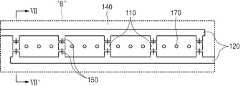
Translated fromKorean도 1은 본 발명의 제1 실시예에 따른 발광 다이오드 모듈의 구조를 나타낸 개략도.1 is a schematic diagram showing the structure of a light emitting diode module according to a first embodiment of the present invention;
도 2는 도 1의 "A" 부분을 확대하여 나타낸 부분 확대도.FIG. 2 is an enlarged view of a portion “A” of FIG. 1 enlarged. FIG.
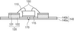
도 3은 도 2의 Ⅲ-Ⅲ'선을 따라 잘라 나타낸 단면도.3 is a cross-sectional view taken along the line III-III ′ of FIG. 2.
도 4는 제1 실시예의 제1 변형예에 따른 발광 다이오드 모듈의 구조를 나타낸 도면.4 is a diagram showing the structure of a light emitting diode module according to a first modification of the first embodiment;
도 5는 제1 실시예의 제2 변형예에 따른 발광 다이오드 모듈의 구조를 나타낸 개략도.5 is a schematic view showing the structure of a light emitting diode module according to a second modification of the first embodiment;
도 6은 도 5의 "B" 부분을 확대하여 나타낸 부분 확대도.FIG. 6 is an enlarged view of a portion “B” of FIG. 5 enlarged. FIG.
도 7은 도 6의 Ⅶ-Ⅶ'선을 따라 잘라 나타낸 단면도.7 is a cross-sectional view taken along the line VII-VII ′ of FIG. 6.
도 8은 제1 실시예에 따른 제3 변형예에 따른 발광 다이오드 모듈의 구조를 나타낸 단면도.8 is a cross-sectional view illustrating a structure of a light emitting diode module according to a third modification example according to the first embodiment.
도 9는 본 발명의 제2 실시예에 따른 발광 다이오드 모듈의 구조를 나타낸 도면.9 is a view showing the structure of a light emitting diode module according to a second embodiment of the present invention.
<도면의 주요 부분에 대한 부호의 설명><Explanation of symbols for main parts of the drawings>
100 : 모듈 110 : LED100: module 110: LED
115 : 접착층 120 : 회로 패턴115: adhesive layer 120: circuit pattern
121 : 도전막 122 : 절연 패턴121: conductive film 122: insulating pattern
130 : 전원 공급부 140 : 금속 박막130: power supply unit 140: metal thin film
140a : 제1 금속 박막 140b : 제2 금속 박막140a: first metal
150 : 와이어 160 : 방열판150: wire 160: heat sink
170 : 구멍 200 : LED 패키지170: hole 200: LED package
본 발명은 발광 다이오드를 이용하여 문자 등을 구현하는 전광판 내지는 표시 장치 등에 적용되는 발광 다이오드 모듈에 관한 것으로, 보다 상세하게는 평탄면 이외의 표시면 상에 대한 전광 표시를 할 수 있는 가요성을 가진 발광 다이오드 모듈에 관한 것이다.BACKGROUND OF THE INVENTION 1. Field of the Invention The present invention relates to a light emitting diode module applied to an electronic display board or a display device that implements letters and the like using light emitting diodes. It relates to a light emitting diode module.
발광 다이오드(Light Emitting Diode, 이하, LED라 한다)는, 전류를 흘리면 발광하는 다이오드로서 반도체의 pn 접합면에 소수 캐리어를 주입시키면 전자가 보다 높은 에너지 준위(level)로 여기하고, 다시 안정된 상태로 되돌아 올 때 가지고 있던 에너지가 빛의 파장대를 가진 전자파로 되어 방사되는 발광 소자를 말한다.A light emitting diode (LED) is a diode that emits light when a current flows, and when a minority carrier is injected into a pn junction surface of a semiconductor, electrons are excited to a higher energy level, and are then stabilized again. It refers to a light emitting device in which the energy it has when it comes back is emitted as an electromagnetic wave having a wavelength band of light.
최근 LED는 비약적인 반도체 기술의 발전에 힘입어, 저휘도의 범용제품에서 탈피하여, 고휘도, 고품질의 제품 생산이 가능해졌다. 또한, 고특성의 청색(blue)과 백색(white) 다이오드의 구현이 현실화됨에 따라서, LED는 차세대 조명원 및 각종의 표시 장치 등으로 그 응용가치가 확대되고 있다.In recent years, thanks to the rapid development of semiconductor technology, LEDs have escaped from general-purpose products with low brightness, enabling production of high-brightness and high-quality products. In addition, as the realization of the blue and white diodes having high characteristics is realized, LEDs are expanding their application value to next-generation lighting sources and various display devices.
이와 같은 LED를 단수 또는 복수로 접합시켜 일정한 크기로 만든 것을 LED 모듈이라 하고, 이는 각종의 표시 장치 및 화상장치의 전광판 등을 구성한다.A single or plural such LEDs are bonded to each other to form a predetermined size, which is called an LED module, which constitutes a display panel of various display devices and image devices.
기존의 LED 모듈은, PCB(인쇄회로기판) 상이나 각질의 보형물 등에 삽입 또는 장착된 것을 다시 주 PCB 상에 장착하여 제작되거나, LED를 일정한 크기의 PCB 상에 배치, 장착하여, 다시 이들 LED를 제어할 수 있는 드라이버(driver)를 장착하여 하나의 모듈을 제작한 후 외부 케이스를 통해 모듈을 고정하여 각각의 모듈을 콘트롤러(controller)와 케이블로 결선하여 제작한다.Existing LED module is manufactured by mounting on the PCB (Printed Circuit Board) or keratinous implant, etc. on the main PCB, or placing and mounting the LED on a PCB of a certain size, and controlling these LEDs again. After installing one driver to make one module, fix the module through the outer case and connect each module with controller and cable.
그런데, 상술한 기존의 LED 모듈은, LED를 단수 또는 복수로 접합시켜 일정한 크기로 형성함으로써, 각종의 표시 장치 및 화상장치의 전광판 등에 적용시킬 수 있었으나, PCB 또는 외부 케이스에 의하여 평면 또는 다각형의 형태로 제작되지 않으므로, 모서리, 모퉁이, 기둥, 곡선 유리 등에는 설치가 어려운 문제가 있다. 즉, 기존의 LED 모듈은, 이들이 적용된 각종의 표시 장치 및 화상장치의 전광판 등의 설치 장소에 있어서 제한적이며, 굴곡이 있는 곡면에 설치시, 전체적인 표시 품질이 저하되는 문제가 있다.By the way, the above-described conventional LED module can be applied to a variety of display devices and electronic display panels of the display device by bonding the LEDs in a singular or plural form to a certain size, but in the form of a flat or polygonal shape by a PCB or an external case. Since it is not made of, there is a problem that is difficult to install, such as corners, corners, columns, curved glass. That is, the existing LED module is limited in the installation place such as the display panel of the various display devices and the image device to which they are applied, and there is a problem that the overall display quality is lowered when installed on the curved curved surface.
또한, 기존의 LED 모듈은, LED를 단수 또는 복수로 접합시켜 제작된 것이기 때문에, 각각의 LED로부터 발생하는 열을 더욱 효율적으로 외부로 방출시킬 필요가 있다.In addition, since a conventional LED module is manufactured by joining a single or plural LEDs, it is necessary to more efficiently release heat generated from each LED to the outside.
따라서, 상기 LED 모듈의 열방출 효율을 향상시킬 수 있는 LED 모듈 관련 기술의 개발이 계속적으로 요구되고 있다.Therefore, there is a continuous demand for the development of LED module related technology that can improve the heat dissipation efficiency of the LED module.
따라서, 본 발명의 목적은 상기와 같은 문제점을 해결하기 위하여, 단수 또는 복수의 LED를 소정의 회로 패턴이 형성된 굴곡이 가능한 연질의 금속 박막에 장착하여, 설치 장소의 제약을 최소화하고, 열방출 효율을 향상시킬 수 있는 LED 모듈을 제공하는 데 있다.Accordingly, an object of the present invention is to install the singular or plural LEDs on a flexible metal thin film having a predetermined circuit pattern formed therein, in order to solve the above problems, to minimize the constraint of the installation site, heat emission efficiency To provide an LED module that can improve the.
상기한 목적을 달성하기 위해, 본 발명은, 가요성을 가지는 금속 박막과, 상기 금속 박막 상에 상기 금속 박막과 절연되도록 인쇄된 회로 패턴과, 상기 회로 패턴이 형성되지 않은 금속 박막 상에 실장된 단수 또는 복수의 LED와, 상기 LED와 회로 패턴의 통전을 위한 와이어 및 상기 LED 상에 형성된 형광체를 포함하는 LED 모듈을 제공한다.In order to achieve the above object, the present invention provides a flexible metal thin film, a circuit pattern printed on the metal thin film to be insulated from the metal thin film, and a metal thin film on which the circuit pattern is not formed. Provided is an LED module including a singular or plural LED, a wire for energizing the LED and a circuit pattern, and a phosphor formed on the LED.
상기한 목적을 달성하기 위한 또 다른 본 발명은, 가요성을 가지는 금속 박막과, 상기 금속 박막 상에 상기 금속 박막과 절연되도록 인쇄된 회로 패턴 및 상기 회로 패턴과 전기적으로 연결되도록 상기 금속 박막 상에 실장된 단수 또는 복수의 LED 패키지를 포함하는 LED 모듈을 제공한다. 이때, 상기 LED 패키지는, 한 쌍의 리드 단자로 형성된 리드프레임과, 상기 리드프레임의 일부가 내측에 수용되도록 합성수지재로 형성된 패키지와, 상기 패키지 내부의 리드프레임 상에 실장된 LED 및 상기 패키지 내부에 충진되어 상기 LED를 보호하는 몰딩재를 포함하여 이루어진 것이 바람직하다.Yet another aspect of the present invention is to provide a metal thin film having flexibility, a circuit pattern printed to be insulated from the metal thin film on the metal thin film, and on the metal thin film to be electrically connected to the circuit pattern. Provided is an LED module including one or more mounted LED packages. In this case, the LED package, a lead frame formed of a pair of lead terminals, a package formed of a synthetic resin material so that a portion of the lead frame is received inside, the LED mounted on the lead frame inside the package and the package inside It is preferably made to include a molding material filled in to protect the LED.
또한, 상기 본 발명의 LED 모듈에서, 상기 금속 박막 상에 상기 금속 박막과 절연되도록 인쇄된 회로 패턴은, 회로 패턴과 동일한 형상으로 이루어진 절연 패턴이 형성된 제1 금속 박막과, 상기 절연 패턴 상에 형성된 도전막 및 상기 도전막과 절연되도록 상기 제1 금속 박막 상에 형성된 제2 금속 박막을 포함하여 이루어진 것이 바람직하다.Further, in the LED module of the present invention, the circuit pattern printed on the metal thin film to be insulated from the metal thin film, the first metal thin film having an insulating pattern formed of the same shape as the circuit pattern and formed on the insulating pattern It is preferable to include a conductive film and a second metal thin film formed on the first metal thin film to be insulated from the conductive film.
또한, 상기 본 발명의 LED 모듈에서, 상기 제1 및 제2 금속 박막은, 반사도 및 방열 특성을 우수하게 하기 위해 구리, 알루미늄, 니켈 및 이들의 합금 중 어느 하나로 형성되어 있는 것이 바람직하다.In addition, in the LED module of the present invention, the first and the second metal thin film is preferably formed of any one of copper, aluminum, nickel and alloys thereof in order to excellent reflectivity and heat dissipation characteristics.
또한, 상기 본 발명의 LED 모듈에서, 상기 LED에서 발생하는 열을 더욱 효과적으로 방출시키기 위하여 상기 회로 패턴이 인쇄되지 않은 금속 박막의 일면에 형성된 가요성을 가지는 방열판을 더 포함하는 것이 바람직하다. 이때, 상기 방열판은, 구리, 알루미늄, 니켈 및 이들의 합금 중 어느 하나로 형성되는 것이 바람직하다.In addition, in the LED module of the present invention, it is preferable to further include a heat sink having flexibility formed on one surface of the metal thin film that the circuit pattern is not printed in order to more effectively release the heat generated from the LED. At this time, the heat sink is preferably formed of any one of copper, aluminum, nickel and alloys thereof.
또한, 상기 본 발명의 LED 모듈에서, 상기 방열판은, 도금법을 사용하여 형성하는 것이 가능하다.In the LED module of the present invention, the heat sink can be formed using a plating method.
또한, 상기 본 발명의 LED 모듈에서, 상기 가요성을 가지는 금속 박막은, 회 로 패턴이 형성되지 않은 부분에 소정 간격 이격되게 형성된 단수 또는 복수의 구멍을 더 포함하여 열방출 효율을 향상시키는 것이 바람직하다.In the LED module of the present invention, the flexible metal thin film may further include a single or a plurality of holes formed at predetermined intervals in a portion where the circuit pattern is not formed to improve heat dissipation efficiency. Do.
이하 첨부한 도면을 참고로 하여 본 발명의 실시예에 대하여 본 발명이 속하는 기술 분야에서 통상의 지식을 가진 자가 용이하게 실시할 수 있도록 상세히 설명한다.Hereinafter, exemplary embodiments of the present invention will be described in detail with reference to the accompanying drawings so that those skilled in the art may easily implement the present invention.
도면에서 여러 층 및 영역을 명확하게 표현하기 위하여 두께를 확대하여 나타내었다. 명세서 전체를 통하여 유사한 부분에 대해서는 동일한 도면 부호를 병기하였다.In the drawings, the thickness of layers, films, panels, regions, etc., are exaggerated for clarity. Like reference numerals designate like parts throughout the specification.
이제 본 발명의 실시예에 따른 LED 모듈에 대하여 도면을 참고로 하여 상세하게 설명한다.Now with reference to the drawings for the LED module according to an embodiment of the present invention will be described in detail.
[[실시예Example 1] One]
먼저, 도 1 내지 도 3을 참고하여 본 발명의 제1 실시예에 따른 LED 모듈에 대하여 상세히 설명한다.First, the LED module according to the first embodiment of the present invention will be described in detail with reference to FIGS. 1 to 3.
도 1은 본 발명의 제1 실시예에 따른 발광 다이오드 모듈의 구조를 나타낸 개략도이고, 도 2는 도 1의 "A" 부분을 확대하여 나타낸 부분 확대도이다.FIG. 1 is a schematic view showing a structure of a light emitting diode module according to a first embodiment of the present invention, and FIG. 2 is an enlarged view showing a portion "A" of FIG.
도 1 및 도 2를 참조하면, 본 발명의 제1 실시예에 따른 LED 모듈(100)은, 가요성을 가지는 금속 박막(140)과, 상기 금속 박막(140) 상에 이와 절연되도록 인쇄되어 회로 패턴(120)과, 상기 회로 패턴(120)이 형성되지 않은 상기 금속 박막 (140) 상에 실장된 단수 또는 복수의 LED(110) 및 상기 LED(110) 상에 형성된 형광체(도시하지 않음)를 포함하여 이루어져 있다. 이때, 상기 LED(110)와 회로 패턴(120)은, 와이어(150)를 통해 전기적으로 연결되어 있다.1 and 2, the
여기서 미설명한 도면부호 130은, 상기 회로 패턴(120)에 전원을 공급하기 위한 전원 공급부를 지칭한다.
이와 같이, 본 발명에 따른 LED 모듈(100)은, 종래 LED 모듈을 이루는 단단한 PCB 기판이 아닌 가요성을 가지는 금속 박막(140)으로 이루어져 있으므로, 전체적인 표시 품질의 저하 없이 모서리, 모퉁이, 기둥, 곡선유리 등과 같은 다양한 곡면을 가진 장소에 설치할 수 있다.As described above, since the
그러면, 이하, 도 3을 참조하여 제1 실시예에 따른 LED 모듈에 대하여 보다 상세히 설명한다. 도 3은 도 2의 Ⅲ-Ⅲ'선을 따라 잘라 나타낸 단면도이다.Next, the LED module according to the first embodiment will be described in more detail with reference to FIG. 3. 3 is a cross-sectional view taken along line III-III ′ of FIG. 2.
도 3에 도시한 바와 같이, 상기 금속 박막(140)은, 제1 금속 박막(140a)과 제2 금속 박막(140b)이 순차 적층되어 이루어져 있다. 이때, 상기 제1 및 제2 금속 박막(140a, 140b)은, LED 모듈 구동시, 각각의 LED(110)에서 발생되는 열을 외부로 용이하게 방출시키기 위하여 방열 특성이 우수한 금속, 예를 들어, 알루미늄, 니켈 및 이들의 합금 등으로 이루어지는 것이 바람직하다.As shown in FIG. 3, the metal
또한, 상기 제1 금속 박막(140a) 상에는 LED 모듈을 구동하기 위한 회로 패턴(120)이 상기 제1 금속 박막(140a)과 절연되도록 형성되어 있다. 보다 상세하게, 상기 회로 패턴(120)은, 우선, 상기 제1 금속 박막(140a) 상에 회로와 동일한 형상으로 이루어진 소정 높이의 절연 패턴(122)이 형성되어 있고, 그 위에 도전막(121) 이 형성되어 있으며, 이에 따라, 상기 절연 패턴(122)을 통해 상기 도전막(121)을 제1 금속 박막(140a)과 전기적으로 절연하는 것이 가능하다.In addition, the
그리고, 상기 제1 금속 박막(140a) 상에 제2 금속 박막(140b)이 형성되어 있으며, 이 또한, 상기 회로 패턴(120)을 이루는 도전막(121)과 절연되도록 형성되어 있다.In addition, a second metal
특히, 본 발명에 따른 상기 제2 금속 박막(140b)은, 방열 특성뿐만 아니라 반사도 또한 높은 금속으로 이루어지는 것이 바람직하다. 이는 상기 제2 금속 박막(140b) 상에 실장된 LED(110)에서 발광하는 광이 발광면이 아닌 그 이외의 면, 즉 제2 금속 박막(140b)으로 흡수 및 산란되어 소멸되는 것을 방지하기 위함이다. 따라서, 본 발명에 따른 LED 모듈은, 방열 효과를 향상시킬 수 있을 뿐만 아니라 광 효율 또한 향상시킬 수 있으므로, 이들이 적용된 각종의 표시 장치 및 화상장치의 전광판 등의 휘도를 향상시켜 표시 품질을 개선하는 것이 가능하다.In particular, the second metal
또한, 상기 제2 금속 박막(140b) 상에 실장된 LED(110)은, 열전도율이 높은 투명 접착층(115)을 통해 고정되는 것이 바람직하다.In addition, the
상기 접착층(115)으로 제2 금속 박막(140b) 상에 고정된 LED(110)는 와이어(150)를 통해 인접한 회로 패턴(120), 즉 한 쌍의 전극과 각각 전기적으로 연결되어 있다.The
그러면, 이하, 본 발명의 제1 실시예에 따른 LED 모듈의 변형예에 대하여, 도 4 내 내지 도 8을 참조하여 설명하기로 한다. 다만, 제1 실시예의 구성 중 제1 실시예와 동일한 부분에 대한 설명은 생략하고, 제1 실시예에서 달라지는 구성에 대해서만 상술하기로 한다.Next, a modified example of the LED module according to the first embodiment of the present invention will be described with reference to FIGS. 4 to 8. However, the description of the same parts as the first embodiment of the configuration of the first embodiment will be omitted, and only the configuration different from the first embodiment will be described in detail.
변형예Variant 1 One
우선, 도 4를 참조하여 본 발명의 제1 실시예에 따른 LED 모듈의 제1 변형예에 대하여 상세히 설명한다. 도 4는 제1 실시예의 제1 변형예에 따른 발광 다이오드 모듈의 구조를 나타낸 도면이다.First, a first modification of the LED module according to the first embodiment of the present invention will be described in detail with reference to FIG. 4. 4 is a view showing the structure of a light emitting diode module according to a first modification of the first embodiment.
도 4에 도시한 바와 같이, 제1 변형예에 따른 LED 모듈은, 제1 실시예에 따른 LED 모듈과 대부분의 구성이 동일하고, 다만, 상기 회로 패턴(120)이 인쇄되지 않은 금속 박막(140)의 일면에 가요성을 가지고 형성된 가용성 방열판(160)을 더 포함한다는 점에서만 제1 실시예와 다르다.As shown in FIG. 4, the LED module according to the first modification has the same configuration as that of the LED module according to the first embodiment, except that the
이때, 상기 방열판(160)은, 방열 효율을 향상시키기 위한 것으로, 방열 특성이 우수한 금속, 예를 들어, 구리, 알루미늄, 니켈 및 이들의 합금 등과 같은 금속으로 형성되는 것이 바람직하다.In this case, the
상기 방열판(160)은, 접착층(도시하지 않음)을 통해 접착하거나, 도금법을 사용하여 형성하는 것이 가능하다.The
이러한 제1 변형예는 제1 실시예에서와 동일한 작용 및 효과를 얻을 수 있을 뿐 아니라, 제1 실시예에 비하여 방열판(160)를 더 포함하고 있기 때문에 방열판(160)에 의해 LED 모듈 구동시, LED(110)에서 발생하는 열을 외부로 용이하게 방출시킬 수 있다는 점에서 제1 실시예보다 더욱 우수한 열방출 효과를 얻을 수 있다.This first modification not only obtains the same operation and effect as in the first embodiment, but also further includes a
변형예Variant 2 2
도 5 내지 도 7을 참조하여 본 발명의 제1 실시예에 따른 LED 모듈의 제2 변형예에 대하여 상세히 설명한다. 도 5는 제1 실시예의 제2 변형예에 따른 발광 다이오드 모듈의 구조를 나타낸 개략도이고, 도 6은 도 5의 "B" 부분을 확대하여 나타낸 부분 확대도이고, 도 7은 도 6의 Ⅶ-Ⅶ'선을 따라 잘라 나타낸 단면도이다.A second modified example of the LED module according to the first embodiment of the present invention will be described in detail with reference to FIGS. 5 to 7. FIG. 5 is a schematic view showing the structure of a light emitting diode module according to a second modification of the first embodiment, FIG. 6 is an enlarged view showing a portion “B” of FIG. 5, and FIG. This is a cross-sectional view taken along the line VII '.
도 5 내지 도 7을 참조하면, 제2 변형예에 따른 LED 모듈은, 제1 실시예에 따른 LED 모듈과 대부분의 구성이 동일하고, 다만, 상기 가요성을 가지는 금속 박막(140) 중 회로 패턴(120)이 형성되지 않은 부분에 소정 간격 이격되게 형성된 단수 또는 복수의 구멍(170)을 더 포함한다는 점에서만 제1 실시예와 다르다.5 to 7, the LED module according to the second modified example has the same configuration as that of the LED module according to the first embodiment, but the circuit pattern of the metal
한편, 도 7에서는 상기 구멍(170)은, 상기 LED(110)가 실장된 부분에도 형성된 상태를 도시하였으나, 이 부분에서는 LED(110)의 특성 및 공정 조건에 따라 상기 구멍(170)을 형성하지 않을 수도 있다.Meanwhile, in FIG. 7, the
또한, 상기 본 발명의 LED 모듈에서, 상기 가요성을 가지는 금속 박막은, 회로 패턴이 형성되지 않은 부분에 소정 간격 이격되게 형성된 단수 또는 복수의 구멍(170)을 더 포함하여 열방출 효율을 향상시키는 것이 바람직하다. 이때, 상기 구멍(170)의 개수 및 간격은 공정 조건에 따라 변경 가능하다.In addition, in the LED module of the present invention, the flexible metal thin film further includes a single or a plurality of
이러한 제2 변형예 또한, 제1 실시예에서와 동일한 작용 및 효과를 얻을 수 있을 뿐 아니라, 제1 변형예와 마찬가지로, 상기 구멍(170)에 의해 LED 모듈 구동시, LED(110)에서 발생하는 열을 외부로 용이하게 방출시킬 수 있다는 점에서 제1 실시예보다 더욱 우수한 열방출 효과를 얻을 수 있다.This second modification can also obtain the same operation and effect as in the first embodiment, and like the first modification, when the LED module is driven by the
변형예Variant 3 3
도 8을 참조하여 본 발명의 제1 실시예에 따른 LED 모듈의 제3 변형예에 대하여 상세히 설명한다. 도 8은 제1 실시예에 따른 제3 변형예에 따른 발광 다이오드 모듈의 구조를 나타낸 단면도이다.A third modification of the LED module according to the first embodiment of the present invention will be described in detail with reference to FIG. 8. 8 is a cross-sectional view illustrating a structure of a light emitting diode module according to a third modification example according to the first embodiment.
도 8을 참조하면, 제3 변형예에 따른 LED 모듈은, 제1 변형예에 따른 LED 모듈과 대부분의 구성이 동일하고, 다만, 상기 가요성을 가지는 금속 박막(140) 중 회로 패턴(120)이 형성되지 않은 부분에 소정 간격 이격되게 형성된 단수 또는 복수의 구멍(170)을 더 포함한다는 점에서만 제1 변형예와 다르다.Referring to FIG. 8, the LED module according to the third modified example has the same configuration as that of the LED module according to the first modified example, except that the
한편, 상기 금속 박막(140)과 방열판(160)은, 모두 구멍(170)을 가지고 있으나, 이는 필요에 따라 어느 하나에만 형성할 수 있다. 즉, LED 모듈의 공정 조건에 따라, 구멍의 개수와 간격 및 형성 위치는 조절 가능하다.Meanwhile, although the metal
[[실시예Example 2] 2]
도 9를 참고하여 본 발명의 제2 실시예에 따른 LED 모듈에 대하여 상세히 설명한다. 다만, 제1 실시예의 구성 중 제1 실시예와 동일한 부분에 대한 설명은 생략하고, 제1 실시예에서 달라지는 구성에 대해서만 상술하기로 한다.An LED module according to a second embodiment of the present invention will be described in detail with reference to FIG. 9. However, the description of the same parts as the first embodiment of the configuration of the first embodiment will be omitted, and only the configuration different from the first embodiment will be described in detail.
도 9는 본 발명의 제2 실시예에 따른 발광 다이오드 모듈의 구조를 나타낸 도면이다.9 is a view showing the structure of a light emitting diode module according to a second embodiment of the present invention.
도 9를 참조하면, 본 발명의 제2 실시예에 따른 LED 모듈(100)은, 제1 실시예에 따른 LED 모듈과 대부분의 구성이 동일하고, 다만, 상기 가요성을 가지는 금속 박막(140) 상에 실장된 LED(110)가 와이어(150)를 통해 회로 패턴(120)과 전기적으로 연결되어 있는 것(도 2 참조)이 아니라, LED 패키지(200)를 금속 박막(140)에 실장하여 회로 패턴(120)과 직접적으로 연결되도록 하는 점에서 제1 실시예와 다르다.Referring to FIG. 9, the
상기 표면 실장형 패키지(200)는, 한 쌍의 리드 단자로 형성된 리드프레임(210)과, 상기 리드프레임(210)의 일부가 내측에 수용되도록 합성수지재로 형성된 패키지(230)와, 상기 패키지(230) 내부의 리드프레임(210) 상에 실장된 LED(110) 및 상기 패키지(230) 내부에 충진되어 상기 LED(110)를 보호하는 몰딩재(220)를 포함하여 이루어진 것이 바람직하다. 이때, 몰딩재(220)는, 색 재현율이 높은 형광체로 이루어지는 것이 바람직하다.The
이와 같이, 제2 실시예에 따른 LED 모듈은, 표면 실장형 패키지(200) 내부에 색 재현율이 높은 형광체로 이루어진 몰딩재(220)를 포함하고 있으므로, LED(110)이 실장된 금속 박막(140) 상에 형광체(도시하지 않음)를 별도로 형성해야 하는 제1 실시예에 비하여 공정을 단순화할 수 있으며, 그로 인해 제조 공정 상의 오염 등을 방지하여 LED 모듈의 신뢰성을 향상시킬 수 있다.As described above, since the LED module according to the second embodiment includes a
한편, 제2 실시예는, 앞서 설명한 제1 실시예의 제1 내지 제3 변형예가 적용 가능하며, 이와 동일한 작용 및 효과를 얻을 수 있다.On the other hand, in the second embodiment, the first to third modified examples of the first embodiment described above can be applied, and the same effects and effects can be obtained.
이상에서 본 발명의 바람직한 실시예에 대하여 상세하게 설명하였지만, 당해 기술 분야에서 통상의 지식을 가진 자라면 이로부터 다양한 변형 및 균등한 타 실시예가 가능하다는 점을 이해할 수 있을 것이다. 따라서, 본 발명의 권리 범위는 이에 한정되는 것은 아니고 다음의 청구범위에서 정의하고 있는 본 발명의 기본 개념을 이용한 당업자의 여러 변형 및 개량 형태 또한 본 발명의 권리범위에 속하는 것이다.Although the preferred embodiments of the present invention have been described in detail above, those skilled in the art will understand that various modifications and equivalent other embodiments are possible therefrom. Accordingly, the scope of the present invention is not limited thereto, and various modifications and improvements of those skilled in the art using the basic concept of the present invention as defined in the following claims also fall within the scope of the present invention.
상기한 바와 같이, 본 발명은, 단수 또는 복수의 LED를 소정의 회로 패턴이 형성된 굴곡이 가능한 연질의 금속 박막에 장착하여 LED 모듈을 형성함으로써, 이를 이용하여 형성된 각종 표시 장치 및 전광판 등의 설치 장소의 제약을 최소화할 수 있다.As described above, the present invention, by mounting a single or a plurality of LEDs on a flexible metal thin film having a predetermined circuit pattern is formed to form an LED module, the installation location of various display devices and display plates formed using the same Can minimize the constraints.
또한, 상기 금속 박막이 열전도율이 우수한 금속으로 이루어져 있으므로, LED에서 발생하는 열의 방출 효율을 향상시켜 LED 모듈의 수명을 최대화시킬 수 있다.In addition, since the metal thin film is made of a metal having excellent thermal conductivity, it is possible to maximize the life of the LED module by improving the efficiency of heat emission from the LED.
Claims (10)
Translated fromKoreanPriority Applications (3)
| Application Number | Priority Date | Filing Date | Title |
|---|---|---|---|
| KR1020060017628AKR100741821B1 (en) | 2006-02-23 | 2006-02-23 | Light emitting diode module |
| US11/644,951US20070194398A1 (en) | 2006-02-23 | 2006-12-26 | Light emitting diode module |
| US12/642,122US20100096661A1 (en) | 2006-02-23 | 2009-12-18 | Light emitting diode module |
Applications Claiming Priority (1)
| Application Number | Priority Date | Filing Date | Title |
|---|---|---|---|
| KR1020060017628AKR100741821B1 (en) | 2006-02-23 | 2006-02-23 | Light emitting diode module |
Publications (1)
| Publication Number | Publication Date |
|---|---|
| KR100741821B1true KR100741821B1 (en) | 2007-07-23 |
Family
ID=38427332
Family Applications (1)
| Application Number | Title | Priority Date | Filing Date |
|---|---|---|---|
| KR1020060017628AExpired - Fee RelatedKR100741821B1 (en) | 2006-02-23 | 2006-02-23 | Light emitting diode module |
Country Status (2)
| Country | Link |
|---|---|
| US (2) | US20070194398A1 (en) |
| KR (1) | KR100741821B1 (en) |
Cited By (2)
| Publication number | Priority date | Publication date | Assignee | Title |
|---|---|---|---|---|
| KR101136054B1 (en) | 2009-09-04 | 2012-04-18 | 파라곤 세미컨덕터 라이팅 테크놀로지 컴퍼니 리미티드 | Led package structure for increasing heat-dissipating effect and light-emitting efficiency and method for manufacturing the same |
| KR101308805B1 (en) | 2009-06-23 | 2013-09-13 | 시티즌 홀딩스 가부시키가이샤 | Light-emitting diode apparatus |
Families Citing this family (3)
| Publication number | Priority date | Publication date | Assignee | Title |
|---|---|---|---|---|
| TWM337834U (en)* | 2007-12-10 | 2008-08-01 | Everlight Electronics Co Ltd | Package structure for light emitting diode |
| TWI553384B (en)* | 2012-12-18 | 2016-10-11 | 鴻海精密工業股份有限公司 | Back light |
| CN108317437B (en)* | 2018-02-12 | 2020-07-31 | 京东方科技集团股份有限公司 | Backlight source, backlight module and display device |
Citations (1)
| Publication number | Priority date | Publication date | Assignee | Title |
|---|---|---|---|---|
| KR20030041777A (en)* | 2001-11-21 | 2003-05-27 | 마츠시타 덴끼 산교 가부시키가이샤 | Thinned circuit substrate and its manufacturing method |
Family Cites Families (10)
| Publication number | Priority date | Publication date | Assignee | Title |
|---|---|---|---|---|
| US3590844A (en)* | 1969-05-07 | 1971-07-06 | Boris Yakovlevich Ladenzon | Device for dividing the flow of liquid into two parts |
| US3757511A (en)* | 1971-05-17 | 1973-09-11 | Motorola Inc | Light emitting diode display for electronic timepiece |
| GB1490978A (en)* | 1973-12-21 | 1977-11-09 | Marconi Co Ltd | Light emitting diode(led)arrays |
| US4488135A (en)* | 1982-07-29 | 1984-12-11 | Schwartz Charles A | Transformer for welding gun |
| JP3713088B2 (en)* | 1996-02-19 | 2005-11-02 | ローム株式会社 | Display device |
| US6614103B1 (en)* | 2000-09-01 | 2003-09-02 | General Electric Company | Plastic packaging of LED arrays |
| US6448582B1 (en)* | 2000-09-21 | 2002-09-10 | Yale University | High modulation frequency light emitting device exhibiting spatial relocation of minority carriers to a non-radiative recombination region |
| US6541800B2 (en)* | 2001-02-22 | 2003-04-01 | Weldon Technologies, Inc. | High power LED |
| TW492202B (en)* | 2001-06-05 | 2002-06-21 | South Epitaxy Corp | Structure of III-V light emitting diode (LED) arranged in flip chip configuration having structure for preventing electrostatic discharge |
| US6812481B2 (en)* | 2001-09-03 | 2004-11-02 | Toyoda Gosei Co., Ltd. | LED device and manufacturing method thereof |
- 2006
- 2006-02-23KRKR1020060017628Apatent/KR100741821B1/ennot_activeExpired - Fee Related
- 2006-12-26USUS11/644,951patent/US20070194398A1/ennot_activeAbandoned
- 2009
- 2009-12-18USUS12/642,122patent/US20100096661A1/ennot_activeAbandoned
Patent Citations (1)
| Publication number | Priority date | Publication date | Assignee | Title |
|---|---|---|---|---|
| KR20030041777A (en)* | 2001-11-21 | 2003-05-27 | 마츠시타 덴끼 산교 가부시키가이샤 | Thinned circuit substrate and its manufacturing method |
Cited By (2)
| Publication number | Priority date | Publication date | Assignee | Title |
|---|---|---|---|---|
| KR101308805B1 (en) | 2009-06-23 | 2013-09-13 | 시티즌 홀딩스 가부시키가이샤 | Light-emitting diode apparatus |
| KR101136054B1 (en) | 2009-09-04 | 2012-04-18 | 파라곤 세미컨덕터 라이팅 테크놀로지 컴퍼니 리미티드 | Led package structure for increasing heat-dissipating effect and light-emitting efficiency and method for manufacturing the same |
Also Published As
| Publication number | Publication date |
|---|---|
| US20100096661A1 (en) | 2010-04-22 |
| US20070194398A1 (en) | 2007-08-23 |
Similar Documents
| Publication | Publication Date | Title |
|---|---|---|
| US10431567B2 (en) | White ceramic LED package | |
| US7872418B2 (en) | Light emitting device and method for manufacturing the same | |
| US8338851B2 (en) | Multi-layer LED array engine | |
| US7997760B2 (en) | Enamel substrate for mounting light emitting elements, light emitting element module, illumination apparatus, display apparatus, and traffic signal | |
| US20090122514A1 (en) | Led module for illumination | |
| EP2023409B1 (en) | Semiconductor light emitting module and device and method of manufacturing the same | |
| KR101006357B1 (en) | Multichip LED Package | |
| US8878228B2 (en) | Method for producing large lighting with power LED | |
| JP2009088190A (en) | Mounting board and LED module | |
| JP2007059894A (en) | Light source mounted with light emitting diode element | |
| KR100741821B1 (en) | Light emitting diode module | |
| KR101051488B1 (en) | Method for manufacturing light emitting diode unit, and light emitting diode unit manufactured by this method | |
| EP2642835A2 (en) | Wiring board device, luminaire, and manufacturing method of the wiring board device | |
| KR20100028134A (en) | Light emitting diode module | |
| KR101363070B1 (en) | Led lighting module | |
| JP2004342791A (en) | Led lamp and led lighting device | |
| KR101051690B1 (en) | Optical package and its manufacturing method | |
| KR100954858B1 (en) | A high-luminance led package and method for manufacturing thereof | |
| KR100660126B1 (en) | Circuit board with heat sink structure | |
| KR100985917B1 (en) | Leadframe with Effective Heat Dissipation Structure for High Power Light Source Lamp, Electronic Device and Manufacturing Method Thereof | |
| KR100850312B1 (en) | Light emitting diode module | |
| JP2010073724A (en) | Light-emitting module | |
| KR100979971B1 (en) | Method for manufacturing light emitting diode unit, and light emitting diode unit manufactured by this method | |
| KR101146659B1 (en) | Optical package and manufacturing method of the same | |
| KR101136392B1 (en) | Optical package and manufacturing method of the same |
Legal Events
| Date | Code | Title | Description |
|---|---|---|---|
| A201 | Request for examination | ||
| PA0109 | Patent application | St.27 status event code:A-0-1-A10-A12-nap-PA0109 | |
| PA0201 | Request for examination | St.27 status event code:A-1-2-D10-D11-exm-PA0201 | |
| R18-X000 | Changes to party contact information recorded | St.27 status event code:A-3-3-R10-R18-oth-X000 | |
| E701 | Decision to grant or registration of patent right | ||
| PE0701 | Decision of registration | St.27 status event code:A-1-2-D10-D22-exm-PE0701 | |
| GRNT | Written decision to grant | ||
| PR0701 | Registration of establishment | St.27 status event code:A-2-4-F10-F11-exm-PR0701 | |
| PR1002 | Payment of registration fee | St.27 status event code:A-2-2-U10-U11-oth-PR1002 Fee payment year number:1 | |
| PG1601 | Publication of registration | St.27 status event code:A-4-4-Q10-Q13-nap-PG1601 | |
| P22-X000 | Classification modified | St.27 status event code:A-4-4-P10-P22-nap-X000 | |
| PN2301 | Change of applicant | St.27 status event code:A-5-5-R10-R11-asn-PN2301 | |
| PN2301 | Change of applicant | St.27 status event code:A-5-5-R10-R11-asn-PN2301 | |
| PN2301 | Change of applicant | St.27 status event code:A-5-5-R10-R14-asn-PN2301 | |
| PR1001 | Payment of annual fee | St.27 status event code:A-4-4-U10-U11-oth-PR1001 Fee payment year number:4 | |
| PR1001 | Payment of annual fee | St.27 status event code:A-4-4-U10-U11-oth-PR1001 Fee payment year number:5 | |
| R18-X000 | Changes to party contact information recorded | St.27 status event code:A-5-5-R10-R18-oth-X000 | |
| PN2301 | Change of applicant | St.27 status event code:A-5-5-R10-R11-asn-PN2301 | |
| FPAY | Annual fee payment | Payment date:20120706 Year of fee payment:6 | |
| PR1001 | Payment of annual fee | St.27 status event code:A-4-4-U10-U11-oth-PR1001 Fee payment year number:6 | |
| PN2301 | Change of applicant | St.27 status event code:A-5-5-R10-R14-asn-PN2301 | |
| FPAY | Annual fee payment | Payment date:20130701 Year of fee payment:7 | |
| PR1001 | Payment of annual fee | St.27 status event code:A-4-4-U10-U11-oth-PR1001 Fee payment year number:7 | |
| R18-X000 | Changes to party contact information recorded | St.27 status event code:A-5-5-R10-R18-oth-X000 | |
| LAPS | Lapse due to unpaid annual fee | ||
| PC1903 | Unpaid annual fee | St.27 status event code:A-4-4-U10-U13-oth-PC1903 Not in force date:20140717 Payment event data comment text:Termination Category : DEFAULT_OF_REGISTRATION_FEE | |
| PC1903 | Unpaid annual fee | St.27 status event code:N-4-6-H10-H13-oth-PC1903 Ip right cessation event data comment text:Termination Category : DEFAULT_OF_REGISTRATION_FEE Not in force date:20140717 | |
| R18-X000 | Changes to party contact information recorded | St.27 status event code:A-5-5-R10-R18-oth-X000 | |
| P22-X000 | Classification modified | St.27 status event code:A-4-4-P10-P22-nap-X000 |