KR100737943B1 - Network-on-chip response signal control device and method - Google Patents
Network-on-chip response signal control device and methodDownload PDFInfo
- Publication number
- KR100737943B1 KR100737943B1KR1020060088652AKR20060088652AKR100737943B1KR 100737943 B1KR100737943 B1KR 100737943B1KR 1020060088652 AKR1020060088652 AKR 1020060088652AKR 20060088652 AKR20060088652 AKR 20060088652AKR 100737943 B1KR100737943 B1KR 100737943B1
- Authority
- KR
- South Korea
- Prior art keywords
- response signal
- transaction
- signal
- slave
- master
- Prior art date
- Legal status (The legal status is an assumption and is not a legal conclusion. Google has not performed a legal analysis and makes no representation as to the accuracy of the status listed.)
- Expired - Fee Related
Links
Images


Classifications
- G—PHYSICS
- G06—COMPUTING OR CALCULATING; COUNTING
- G06F—ELECTRIC DIGITAL DATA PROCESSING
- G06F15/00—Digital computers in general; Data processing equipment in general
- G06F15/76—Architectures of general purpose stored program computers
- G06F15/78—Architectures of general purpose stored program computers comprising a single central processing unit
- G06F15/7807—System on chip, i.e. computer system on a single chip; System in package, i.e. computer system on one or more chips in a single package
- G06F15/7825—Globally asynchronous, locally synchronous, e.g. network on chip
- H—ELECTRICITY
- H04—ELECTRIC COMMUNICATION TECHNIQUE
- H04L—TRANSMISSION OF DIGITAL INFORMATION, e.g. TELEGRAPHIC COMMUNICATION
- H04L12/00—Data switching networks
- H04L12/28—Data switching networks characterised by path configuration, e.g. LAN [Local Area Networks] or WAN [Wide Area Networks]
Landscapes
- Engineering & Computer Science (AREA)
- Computer Hardware Design (AREA)
- Theoretical Computer Science (AREA)
- General Engineering & Computer Science (AREA)
- Computing Systems (AREA)
- Microelectronics & Electronic Packaging (AREA)
- Physics & Mathematics (AREA)
- General Physics & Mathematics (AREA)
- Signal Processing (AREA)
- Computer Networks & Wireless Communication (AREA)
- Data Exchanges In Wide-Area Networks (AREA)
- Information Transfer Systems (AREA)
- Programmable Controllers (AREA)
Abstract
Translated fromKoreanDescription
Translated fromKorean도 1은 본 발명에 따른 NoC 응답 신호 제어에 대한 일 실시예 구성 블록도이다.1 is a block diagram of an embodiment of the NoC response signal control according to the present invention.
도 2는 도 1에 도시한 NIS에 대한 상세 구성 블록도이다.FIG. 2 is a detailed block diagram of the NIS shown in FIG. 1.
도 3은 도 1에 도시한 NIM에 대한 상세 구성 블록도이다.3 is a detailed block diagram of the NIM shown in FIG.
도 4는 본 발명이 NoC 라우터의 로컬 영역에 적용된 경우에 대한 일 예시도이다.4 is an exemplary diagram illustrating a case where the present invention is applied to a local area of a NoC router.
도 5는 기존의 라우터를 통한 응답 대기시간과 본 발명에 따른 응답 대기시간을 비교한 일 예의 파형도이다.5 is a waveform diagram of an example in which a response wait time through a conventional router is compared with a response wait time according to the present invention.
도 6은 본 발명에 따른 NoC 응답 신호 제어 방법에 대한 일 실시예 동작 흐름도이다.6 is a flowchart illustrating an embodiment of a method for controlling a NoC response signal according to the present invention.
도 7은 도 6에 도시한 S610 단계에 대한 일 실시예 상세 동작 흐름도이다.7 is a flowchart illustrating a detailed operation of an embodiment of step S610 illustrated in FIG. 6.
도 8은 도 6에 도시한 S620 단계에 대한 일 실시예 상세 동작 흐름도이다.8 is a flowchart illustrating a detailed operation of an embodiment of step S620 illustrated in FIG. 6.
<도면의 주요 부분에 대한 부호의 설명><Explanation of symbols for the main parts of the drawings>
110,310: NI 마스터110,310: NI Master
111,340: 디코더111,340: Decoder
120: NoC 라우터120: NoC router
130,220: NI 슬레이브130,220: NI slave
131, 260: 패킷 빌더131, 260: Packet Builder
140,270,370: 응답 신호 와이어140,270,370: response signal wire
본 발명은 NoC(Network-on-Chip) 응답신호 제어에 관한 것으로, 더욱 상세하게는 응답 신호에 의해 발생되는 NoC 대기시간(Latency)을 줄이기 위한 NoC 응답신호 제어 장치 및 그 방법에 관한 것이다.The present invention relates to network-on-chip response signal control, and more particularly, to an apparatus and method for controlling a NoC response signal for reducing a NoC latency caused by a response signal.
컴퓨터, 통신, 방송 등이 점차 통합되는 컨버전스(Convergence)화에 따라, 기존 ASIC(Application Specific IC: 주문형 반도체)과 ASSP(Application-Specific Standard Product: 특정용도 표준제품)의 수요가 SoC(System-on-Chip)로 전환되어 가고 있는 추세이다. 또한, IT(Information Technology)기기의 경박 단소화 및 고기능화 추세도 SoC 산업을 촉진시키는 요인이 되고 있다.As convergence becomes increasingly integrated with computers, communications, and broadcasting, the demand for existing Application Specific ICs (ASICs) and Application-Specific Standard Products (ASSPs) is increasing. -Chip is moving towards. In addition, the trend toward lighter and shorter and more functionalized IT (Information Technology) devices is also accelerating the SoC industry.
SoC는 기존의 여러가지 기능을 가진 복잡한 시스템을 하나의 칩으로 구현한 기술 집약적 반도체 기술이다. SoC의 현실화를 위해 많은 기술들이 연구되고 있으며, 특히 칩 내에 내재되어 있는 여러 지능소자(intellectual property: IP)들을 연결하는 방안이 매우 중요한 사항으로 대두되고 있다.SoC is a technology-intensive semiconductor technology that implements a complex system with various functions in one chip. Many technologies have been studied for the realization of SoC, and in particular, the method of connecting various intellectual property (IP) inherent in the chip has emerged as an important issue.
IP들을 연결하기 위한 기술로는 버스를 기반으로 한 연결 방식이 주를 이루 고 있는 실정이다. 그러나, 칩의 집적도가 높아지고 IP간의 정보 흐름의 양이 급격히 증가함에 따라, 버스구조를 이용한 SoC는 그 구조적 한계에 도달하였다.As a technology for connecting IPs, a bus-based connection method is mainly used. However, as chip density increases and the amount of information flow between IPs increases rapidly, SoCs using a bus structure have reached their structural limits.
이와 같이 버스구조를 이용한 SoC의 구조적 한계를 해소하기 위한 방안으로, 일반적인 네트워크 기술을 칩 내에 응용하여 IP들을 연결하는 방식인 NoC(Network-on-Chip) 기술이 새롭게 제시되었다.As a way to solve the structural limitations of SoC using a bus structure, NoC (Network-on-Chip) technology, a method of connecting IPs by applying general network technology in a chip, has been newly proposed.
NoC는 기존 버스 구조의 구조적 한계를 극복하고자 만들어진 네트워크 형태의(network style) OCI(On-Chip Interconnect)로서, NoC를 통해 고속/고성능/저전력의 SoC를 구현할 수 있다.NoC is a network-style On-Chip Interconnect (OCI) designed to overcome the structural limitations of existing bus structures. NoC enables high-speed / high-performance / low-power SoCs.
하지만, NoC는 IP들간 패킷을 전달하기 위해 많은 대기시간(Latency)을 필요로 한다. 즉, 마스터 IP로부터 발생된 신호(읽기/쓰기 어드레스 신호, 쓰기데이터 신호)를 마스터 NI(Network Interface)에서 패킷화하여 슬레이브 IP로 전송하거나, 마찬가지로 슬레이브 IP로부터 발생한 신호(읽기데이터 신호, 응답 신호)들을 슬레이브 NI에서 패킷화하여 전송하는 과정에 많은 대기시간을 필요로 하게 된다.However, NoC requires a lot of latency to deliver packets between IPs. That is, signals generated from the master IP (read / write address signal, write data signal) are packetized by the master NI (Network Interface) and transmitted to the slave IP, or similarly signals generated from the slave IP (read data signal and response signal). It takes a lot of waiting time to packetize and transmit them to slave NI.
즉, 마스터 IP로부터 발생된 패킷을 슬레이브 IP로 전송하고, 슬레이브 IP로부터 상기 패킷에 대한 응답 신호를 전송하는 과정에 많은 대기시간을 필요로 한다.In other words, a lot of waiting time is required in the process of transmitting a packet generated from the master IP to the slave IP, and transmitting a response signal for the packet from the slave IP.
종래 패킷 대기시간을 줄이기 위한 방법으로 라우터끼리 직접 연결하는 경로를 만들어 줌으로써, 패킷 대기시간을 줄일 수 있었다.In the conventional method for reducing the packet waiting time, the packet waiting time could be reduced by making a direct connection path between routers.
하지만, 이런 종래 방법은 많은 라우터끼리 직접 연결하기 때문에 와이어 복잡도(Wire Complexity)가 증가하고, 게이트 카운트(Gate Count)가 증가하는 단점이 있다.However, this conventional method has a disadvantage in that wire complexity increases and gate count increases because many routers connect directly to each other.
또한, 기존의 AXI Interconnect와 NoC 각각의 응답 시간을 비교할 때 NoC의 응답 시간이 AXI Interconnect의 응답 시간에 비해 많이 걸리는 단점이 있다. 예를 들어, 마스터와 슬레이브 IP가 각각 1개씩 연결되어 있는 1:1 구조에서의 AXI Interconnect의 응답시간에 1 클럭을 필요한 반면, NoC의 응답시간에 9 클럭 정도를 필요로 한다.In addition, when comparing the response time of the conventional AXI interconnect and the NoC, the response time of the NoC is much longer than that of the AXI interconnect. For example, one clock is required for the response time of the AXI Interconnect in a 1: 1 structure in which one master and one slave IP are connected, while about 9 clocks are required for the response time of the NoC.
본 발명은 상술한 바와 같은 종래기술의 문제점을 해결하기 위해 안출된 것으로서, 마스터 IP로부터 발생된 쓰기 트랜잭션(transaction)에 대한 응답 신호의 대기시간을 줄일 수 있는 NoC 응답 신호 제어 장치 및 그 방법을 제공하는 것을 목적으로 한다.The present invention has been made to solve the problems of the prior art as described above, and provides an apparatus and method for controlling a NoC response signal that can reduce the latency of the response signal for a write transaction generated from the master IP It aims to do it.
또한, 본 발명은 NoC의 응답 신호에 대한 대기시간을 줄이면서 구현 비용을 최소화하는 것을 목적으로 한다.In addition, the present invention aims to minimize the implementation cost while reducing the latency for the response signal of the NoC.
또한, 본 발명은 낮은 와이어 복잡도로 패킷 대기시간을 감소시키는 것을 목적으로 한다.It is also an object of the present invention to reduce packet latency with low wire complexity.
상기의 목적을 달성하고 종래기술의 문제점을 해결하기 위하여, 본 발명의 NoC 응답신호 제어 장치는 슬레이브(slave) IP(Intellectual Property)로부터 응답 신호가 입력된 경우 응답 신호 와이어를 통해 상기 응답 신호에 대한 활성화 신호를 출력하는 NI 슬레이브 및 상기 NI 슬레이브와 직접 연결된 상기 응답 신호 와이 어를 통해 상기 활성화 신호가 입력된 경우 상기 응답 신호에 대한 트랜잭션(transaction)을 생성하여 마스터(master) IP로 출력하는 NI(Network Interface) 마스터를 포함하는 것을 특징으로 한다.In order to achieve the above object and to solve the problems of the prior art, the NoC response signal control apparatus of the present invention, when a response signal is input from a slave IP (slave) Intellectual Property (IP) for the response signal through a response signal wire When the activation signal is input through the NI slave for outputting an activation signal and the response signal wire directly connected to the NI slave, the NI generates a transaction for the response signal and outputs it to a master IP. Network Interface) is characterized in that it comprises a master.
본 발명의 일 실시예에 따른 NoC 응답 신호 제어 방법은 NI(Network Interface) 슬레이브(slave)에서 슬레이브 IP(Intellectual Property)로부터 응답 신호가 입력된 경우 응답 신호 와이어를 통해 상기 응답 신호에 대한 활성화 신호를 출력하는 단계 및 NI 마스터(master)에서 상기 NI 슬레이브와 직접 연결된 상기 응답 신호 와이어를 통해 상기 활성화 신호가 입력된 경우 상기 응답 신호에 대한 트랜잭션(transaction)을 생성하여 마스터 IP로 출력하는 단계를 포함하는 것을 특징으로 한다.The method for controlling a NoC response signal according to an embodiment of the present invention provides an activation signal for the response signal through a response signal wire when a response signal is input from a slave IP (IP) in a NI (Network Interface) slave. And outputting a transaction to the master IP when the activation signal is input through the response signal wire directly connected to the NI slave in an NI master. It is characterized by.
이때, 상기 응답 신호 와이어는 1비트 와이어일 수 있다.In this case, the response signal wire may be a 1-bit wire.
이때, 상기 트랜잭션은 AXI(Advanced Extensible Interface) 트랜잭션일 수 있다.In this case, the transaction may be an Advanced Extensible Interface (AXI) transaction.
이때, 상기 NI 마스터에서 상기 NI 슬레이브와 직접 연결된 상기 응답 신호 와이어를 통해 상기 활성화 신호가 입력된 경우 상기 응답 신호에 대한 트랜잭션을 생성하여 마스터 IP로 출력하는 단계는 상기 마스터 IP로부터 입력된 aWID 신호를 추가적으로 이용하여 상기 응답 신호에 대한 트랜잭션을 생성하고, 상기 생성된 응답 신호에 대한 트랜잭션을 상기 마스터 IP로 출력할 수 있다.In this case, when the activation signal is input through the response signal wire directly connected to the NI slave in the NI master, generating a transaction for the response signal and outputting the transaction to the master IP may include aWID signal input from the master IP. In addition, a transaction for the response signal may be generated and the transaction for the generated response signal may be output to the master IP.
이하, 본 발명에 따른 바람직한 실시예를 첨부된 도면을 참조하여 상세하게 설명한다.Hereinafter, exemplary embodiments of the present invention will be described in detail with reference to the accompanying drawings.
본 발명에서 사용되는 트랜잭션은 AXI(Advanced Extensible Interface), AHB(AMBA High-Performance Bus) 및 OCP(Open Core Protocol) 트랜잭션을 모두 포함할 수 있지만, 본 발명의 상세한 설명에서는 AXI 트랜잭션에 한정하여 설명한다.Transactions used in the present invention may include both Advanced Extensible Interface (AXI), AMBA High-Performance Bus (AHB), and Open Core Protocol (OCP) transactions, but the detailed description of the present invention will be limited to AXI transactions. .
일반적으로 NI(Network Interface) 마스터에서 마스터 IP로 출력하는 응답 AXI 트랜잭션은 4[bit]의 bID 신호, 2[bit]의 BResp 신호 및 1[bit]의 BValid 신호를 포함한다.In general, the response AXI transaction output from the NI (Network Interface) master to the master IP includes a 4 [bit] bID signal, a 2 [bit] BResp signal, and a 1 [bit] BValid signal.
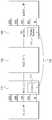
도 1은 본 발명에 따른 NoC 응답 신호 제어 장치에 대한 일 실시예 구성 블록도이다.1 is a block diagram of an embodiment of a NoC response signal control apparatus according to the present invention.
도 1을 참조하면, 본 발명에 따른 NoC 응답 신호 제어 장치는 NI 마스터(이하, "NIM"이라 칭함)(110), NoC 라우터(120) 및 NI 슬레이브(이하, "NIS"이라 칭함)(130)를 포함한다.Referring to FIG. 1, an apparatus for controlling a NoC response signal according to the present invention includes an NI master (hereinafter referred to as "NIM") 110, a
NIM(110)은 마스터 IP로부터 발생된 읽기 어드레스, 쓰기 어드레스 또는 쓰기 데이터 AXI 트랜잭션을 입력받아 NoC 패킷으로 변환하여 NoC 라우터(120)로 출력하고, NIS(130)와 직접 연결된 응답 신호 와이어(140)로부터 응답 신호에 대한 활성화 신호가 입력된 경우 응답 트랜잭션(B)을 마스터 IP로 출력한다.The NIM 110 receives a read address, a write address, or a write data AXI transaction generated from the master IP, converts it into a NoC packet, outputs it to the
이때, 응답 신호 와이어(140)는 1[bit]의 와이어일 수 있고, NIM(110)은 1[bit]의 응답 신호 와이어를 통해 응답 신호에 대한 활성화 신호를 입력받는다.At this time, the
이때, 응답 신호 와이어(140)는 NIM(110)에 구비된 디코더(decoder)(111)에 직접 연결되고, 디코더로 응답 신호에 대한 활성화 신호가 입력되면 디코더에서 NIM으로 입력된 AXI 트랜잭션에 포함된 aWID 신호를 추가적으로 이용하여 응답 트 랜잭션을 생성하여 마스터 IP로 출력한다. 즉, 디코더(111)에서 4[bit]의 bID 정보를 NIM에 저장된 aWID 신호로 하여 응답 AXI 트랜잭션을 생성하다.In this case, the
NoC 라우터(120)는 NIM(110)으로부터 입력된 NoC 패킷을 NIS(130)로 출력하고, NIS(130)로부터 입력된 NoC 패킷을 NIM(110)으로 출력한다.The
NIS(130)는 NoC 라우터(120)로부터 입력된 읽기 또는 쓰기에 대한 패킷을 입력받아 읽기 또는 쓰기 AXI 트랜잭션으로 변환한 후 슬레이브 IP로 출력하고, 슬레이브 IP로부터 상기 마스터 IP로부터 발생된 AXI 트랜잭션에 대한 "OKAY"의 응답 신호가 입력된 경우 1 [bit]의 응답 신호 와이어(140)를 통해 응답 신호에 대한 활성화 신호를 NIM(110)으로 출력한다. 물론, 슬레이브 IP로부터 "OKAY"의 응답 신호가 입력되지 않는 경우에는 기존의 처리 과정을 수행하며, 기존의 처리 과정은 이 기술 분야에 종사하는 당업자라면 알 수 있는 기술 사항이므로 설명은 생략한다.The NIS 130 receives a packet for a read or write input from the
이때, NIM에 구비된 디코더와 직접 연결된 응답 신호 와이어는 NIM에 구비된 패킷 빌더(packet builder)(131)에 직접 연결되고, NIS(130)로 "OKAY"의 응답 신호가 입력되면 패킷 빌더(131)에서 응답 신호에 대한 패킷을 생성하지 않고, 응답 신호에 대한 활성화 신호를 생성하여 응답 신호 와이어(140)를 통해 NIM의 디코더(111)로 출력한다.In this case, the response signal wire directly connected to the decoder provided in the NIM is directly connected to the
이와 같은 구성을 갖는 본 발명에 대한 동작을 동작을 도 2와 도 3을 참조하여 설명한다. 여기서, 본 발명에 대한 동작은 마스터 IP로부터 발생된 AXI 트랜잭션이 NIM과 라우터를 통하고, NIS를 거쳐 다시 NIM까지 전달되는 과정 예를 들어, 읽기 어드레스, 쓰기 어드레스 AXI 트랜잭션 또는 읽기데이터, 쓰기데이터 AXI 트랜잭션에 대한 패킷이 NoC 라우터를 통해 NIM까지 전달되는 과정은 기존 패킷 처리 과정을 통해 수행되기 때문에 마스터 IP로부터 발생된 쓰기 AXI 트랜잭션에 대한 응답 AXI 트랜잭션을 생성하는 과정에 대해서만 설명한다.An operation of the present invention having such a configuration will be described with reference to FIGS. 2 and 3. Here, the operation of the present invention is a process in which the AXI transaction generated from the master IP is passed through the NIM and the router, and then through the NIS to the NIM. For example, a read address, a write address AXI transaction or read data, a write data AXI. Since the process of passing a packet for a transaction to the NIM through the NoC router is performed through the existing packet processing process, only the process of generating an AXI transaction in response to a write AXI transaction generated from the master IP is described.
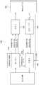
도 2는 본 발명에 따른 NIS에 대한 상세 구성 블록도이다.2 is a detailed block diagram of an NIS according to the present invention.
도 2를 참조하면, NIS(220)는 패킷 수신부(230), 디코더(240), 패킷 빌더(260) 및 아비터(250)를 포함한다.Referring to FIG. 2, the
패킷 수신부(230)는 NoC 라우터(210)로부터 수신된 플릿(flit)(또는 패킷) 형태로 들어오는 신호에 대응하는 플릿 채널로 입력된 신호를 전송한다.The
디코더(240)는 각 플릿 채널별로 플릿에 대응하는 AXI 트랜잭션으로 변환하여 슬레이브 IP로 출력한다. 이때, 디코더는 쓰기 어드레스 패킷과 쓰기 데이터 패킷을 결합하는 쓰기 어드레스 CAM(write Address CAM)을 포함한다.The
아비터(250)는 패킷 빌더(260)로부터 입력된 플릿 중 하나를 선택하여 NoC 라우터(210)로 출력한다.The
패킷 빌더(260)는 슬레이브 IP로부터 입력된 응답 신호 및 읽기 데이터에 대한 AXI 트랜잭션을 플릿(또는 패킷) 형태로 변환하여 아비터(250)로 출력하는 것으로, 본 발명에 따른 패킷 빌더(260)는 슬레이브 IP로부터 응답 신호가 입력되면 그 입력된 응답신호가 "OKAY"인지 판단하고, "OKAY"인 경우에만 패킷 빌더에 직접 연결된 1[bit]의 응답 신호 와이어(270)를 활성화시켜 응답 신호 와이어(270)로 응답 신호에 대한 활성화 신호 예를 들어, '1'을 출력한다. 이때, 응답 신호는 BReady 신호와 BValid 신호의 핸드쉐이크(handshake)에 의해 생성되고, 응답 신호에 대한 활성화 신호는 BResp 신호가 "OKAY"이면서 BValid 신호가 "High"인 것을 의미한다.The
이때, 응답 신호에 대한 활성화 신호는 응답 신호 와이어가 연결된 NIM의 디코더로 출력된다.At this time, the activation signal for the response signal is output to the decoder of the NIM to which the response signal wire is connected.
이때, 본 발명에 따른 NIS 패킷 빌더는 슬레이브 IP로부터 입력된 응답 신호만을 판단하여 동작하며, 기타 다른 신호 예를 들어, 자주 발생하지 않는 에러 신호인 EXOKAY, SLVERR, DECERR 등에 대한 신호는 기존 방식과 동일하게 패킷 형식으로 변환하여 NoC 라우터를 통해 전송한다.At this time, the NIS packet builder according to the present invention operates only by determining a response signal input from the slave IP, and other signals, for example, signals for EXOKAY, SLVERR, DECERR, etc., which are not frequently generated, are the same as the conventional method. The packet is converted into a packet format and transmitted through the NoC router.
도 3은 본 발명에 따른 NIM에 대한 상세 구성 블록도이다.3 is a detailed block diagram of a NIM according to the present invention.
도 3을 참조하면, NIM(310)은 패킷 빌더(320), 아비터(330), 패킷 수신부(350) 및 디코더(340)를 포함한다.Referring to FIG. 3, the
아비터(330) 및 패킷 수신부(350)는 도 2에 도시한 아비터 및 패킷 수신부와 같은 기능을 수행하기에 설명하지 않는다.The
패킷 빌더(320)는 마스터 IP로부터 발생된 읽기 어드레스, 쓰기 어드레스 또는 쓰기 데이터 AXI 트랜잭션을 각각의 채널에 맞는 플릿(또는 패킷) 형태로 변환하여 아비터(330)로 전송한다.The
디코더(340)는 각 플릿 채널별로 플릿에 대응하는 AXI 트랜잭션으로 변환하여 마스터 IP로 출력하는 것으로, 본 발명에 따른 디코더(340)는 NIS의 패킷 빌더와 응답 신호 와이어(370)를 통해 직접 연결되고, 응답 신호 와이어(370)로 응답 신호에 대한 활성화 신호가 입력되면 패킷 빌더(320) 내에서 어드레스 에러를 체크 하기 위해 저장하고 있는 aWID 신호(WADDR Error Flit)를 이용하여 응답 AXI 트랜잭션을 생성하여 마스터 IP로 출력한다. 이때, 디코더(340)로 응답 신호에 대한 활성화 신호가 입력된 경우는 BResp 신호가 "OKAY"이면서 BValid 신호가 "High"인 것을 의미하기 때문에 WADDR Error Flit에 포함된 aWID 신호인 4[bit]의 bID 신호, 2[bit]의 BResp 신호 및 1[bit]의 BValid 신호의 응답 AXI 트랜잭션 신호를 생성하여 마스터 IP로 출력한다.The
본 발명에 따른 일 실시예에서 알 수 있듯이, 마스터 IP로부터 발생된 쓰기 AXI 트랜잭션에 대한 응답 AXI 트랜잭션이 NIS의 아비터, NoC 라우터 및 NIM의 패킷 수신부를 거치지 않고 NIM에서 응답 신호 와이어를 통해 NIS로부터 응답 신호에 대한 활성화 신호를 직접 입력받아 응답 AXI 트랜잭션을 생성하여 마스터 IP로 출력하기 때문에 응답 대기시간을 줄일 수 있다.As can be seen in one embodiment according to the present invention, a response to a write AXI transaction originating from a master IP is answered by the AXI transaction from the NIS via a response signal wire at the NIM without going through the NIS's arbiter, NoC router and NIM's packet receiver. The response latency can be reduced by directly receiving the activation signal for the signal and generating a response AXI transaction to the master IP.
도 4는 본 발명에 따른 NoC 응답신호 제어 장치를 로컬(local)한 부분에 적용한 일 예시도이다.4 is an exemplary diagram in which the apparatus for controlling a NoC response signal according to the present invention is applied to a local part.
도 4에서 알 수 있듯이, 본 발명에 따른 NoC 응답신호 제어 장치가 동일한 라우터(Router)에 연결된 NIM과 NIS에 적용된 것을 알 수 있다. 즉, 동일한 라우터에 연결된 IP들간 데이터 교환이 자주 발생하는 경우에 적용될 수 있고, 1[bit]의 응답 신호 와이어만 NIM과 NIS에 직접 연결하면 되기 때문에 와이어의 복잡도는 최소화되면서 응답 신호에 대한 대기시간을 줄일 수 있는 장점이 있다.As can be seen in Figure 4, it can be seen that the NoC response signal control apparatus according to the present invention is applied to the NIM and NIS connected to the same router (Router). In other words, it can be applied when data exchange occurs frequently between IPs connected to the same router. Since only 1 [bit] response signal wire needs to be directly connected to NIM and NIS, latency of response signal is minimized while wire complexity is minimized. There is an advantage to reduce.
여기서, 로컬한 부분이 아닌 서로 다른 라우터와 연결된 IP들 간에 통신이 이루어진 경우에는 기존 처리 과정을 통해 수행되는 것은 자명하다.In this case, when communication is performed between IPs connected to different routers rather than a local part, it is obvious that the communication is performed through an existing process.
도 5는 기존의 라우터를 통한 응답 대기시간과 본 발명에 따른 응답 대기시간을 비교한 일 예의 파형도로서, 동일한 라우터에 연결된 IP들간의 응답 대기시간에 관한 파형도이다.FIG. 5 is a waveform diagram illustrating an example of a comparison of response latency through a conventional router and response latency according to the present invention. FIG. 5 is a waveform diagram of response latency between IPs connected to the same router.
도 5에서 알 수 있듯이, 기존 방식에 의한 응답 대기시간(495[ns])에 비해 본 발명에 따른 응답 대기시간(415[ns])이 작은 것을 알 수 있다. 따라서, IP들간 데이터 교환이 자주 발생하게 되면 그만큼의 응답 대기시간이 줄어들게 되어 전체 대기시간을 줄일 수 있다.As can be seen in FIG. 5, it can be seen that the response waiting time 415 [ns] according to the present invention is smaller than the response waiting time 495 [ns] according to the conventional method. Therefore, if data exchange between IPs occurs frequently, the response latency is reduced, and the overall latency can be reduced.
또한, 본 발명은 로컬한 부분이 아닌 글로벌(global)한 부분에도 적용될 수 있다. 즉, 한 NIM과 NoC를 구성하는 모든 NIS 사이에 1[bit]의 응답 신호 와이어를 직접 연결하고, 한 NIS와 NoC를 구성하는 모든 NIM 사이에 1[bit]의 응답 신호 와이어를 직접 연결하여 본 발명에 따른 NoC 응답 신호 제어 장치를 구성할 수도 있다. 여기서, 응답 신호 와이어를 글로벌한 부분에 적용하였기 때문에 서로 다른 라우터에 연결된 IP들 간에 통신 시에도 라우터를 거치지 않고, 응답 신호 와이어를 통해 응답 신호에 대한 활성화 신호를 출력하여 응답 신호에 대한 대기 시간을 줄일 수 있다.In addition, the present invention can be applied to a global part rather than a local part. That is, 1 [bit] response signal wire is directly connected between one NIM and all NIS constituting NoC, and 1 [bit] response signal wire is directly connected between one NIS and all NIM constituting NoC. The NoC response signal control device according to the invention can also be configured. Here, since the response signal wire is applied to the global part, even when communicating between IPs connected to different routers, a waiting time for the response signal is output by outputting an activation signal for the response signal through the response signal wire without passing through the router. Can be reduced.
이때, 본 발명을 글로벌한 부분에 적용하는 경우에는 비록 와이어 복잡도가 증가하고, 차지하는 면적이 커질 수 있지만, 대기시간이 시스템의 성능에 지대한 영향을 미치는 경우에 적용할 수 있다.In this case, when the present invention is applied to the global part, although the wire complexity and the area to be occupied may be increased, the present invention may be applied to the case where the latency greatly affects the performance of the system.
물론, 글로벌한 부분에 적용할 경우 NoC를 구성하는 "NIM의 개수ⅹNIS의 개수"만큼의 응답 신호 와이어가 필요한 것은 자명하다.Of course, when applied to the global part, it is obvious that as many response signal wires as the number of NIMs < RTI ID = 0.0 > NIS < / RTI >
반면, 본 발명에 따른 NIM이 멀티플 아웃스탠딩(multiple outstanding)을 지원하는 경우에는 쓰기 어드레스가 발생한 순서대로 응답 신호에 대한 활성화 신호가 NIM의 디코더로 도착한다고 볼 수 없기 때문에 1[bit]의 응답 신호 와이어를 사용하면 도 3에 도시한 WADDR Error Flit 정보에 포함된 aWID 신호를 사용할 수 없다. 따라서, NIM이 멀티플 아웃스탠딩을 지원하는 경우에는 NIS로부터 4[bit]의 bID 정보를 직접 수신하기 위해 5[bit]의 응답 신호 와이어를 사용해야 한다. 즉, 슬레이브 IP로부터 "OKAY" 응답 신호가 NIS의 패킷 빌더로 입력되면, NIS 패킷 빌더에서 4[bit]의 bID 정보가 포함된 5[bit]의 응답 신호에 대한 활성화 신호를 NIM의 디코더로 출력한다.On the other hand, when the NIM according to the present invention supports multiple outstanding, since the activation signal for the response signal does not appear to arrive at the decoder of the NIM in the order in which the write addresses occur, the response signal of 1 [bit]. If a wire is used, the aWID signal included in the WADDR Error Flit information shown in FIG. 3 cannot be used. Therefore, when the NIM supports multiple outstandings, 5 [bit] response signal wires must be used to directly receive 4 [bit] bID information from the NIS. That is, when the "OKAY" response signal is inputted from the slave IP to the packet builder of the NIS, the NIS packet builder outputs an activation signal for a 5 [bit] response signal including 4 [bit] bID information to the decoder of the NIM. do.
이와 같이 본 발명은 NoC를 구성하는 NIM의 디코더와 NIS의 패킷 빌더를 1[bit] 또는 5[bit]의 응답 신호 와이어로 직접 연결하고, 응답 신호에 대한 활성화 신호가 발생한 경우 NIS의 아비터, NoC 라우터 및 NIM의 패킷 수신부를 거치지 않고 NIM의 디코더에서 응답 AXI 트랜잭션을 생성하여 마스터 IP로 출력하기 때문에 응답 신호에 의한 대기시간을 줄일 수 있다.As described above, the present invention directly connects the decoder of NIM constituting the NoC and the packet builder of NIS with a response signal wire of 1 [bit] or 5 [bit], and when an activation signal for the response signal is generated, the NIS arbiter and NoC Since the response AXI transaction is generated by the NIM decoder and output to the master IP without going through the router and the packet receiver of the NIM, the latency caused by the response signal can be reduced.
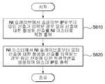
도 6은 본 발명에 따른 NoC 응답 신호 제어 방법에 대한 일 실시예 동작 흐름도이다.6 is a flowchart illustrating an embodiment of a method for controlling a NoC response signal according to the present invention.
도 6을 참조하면, 본 발명에 따른 NoC 응답 신호 제어 방법은 NIS에서 슬레이브 IP로부터 응답 신호가 입력된 경우 그 입력된 응답 신호에 대한 활성화 신호를 NIM으로 직접 출력한다(S610).Referring to FIG. 6, when the response signal is input from the slave IP in the NIS, the method for controlling the NoC response signal according to the present invention directly outputs an activation signal for the input response signal to the NIM (S610).
이때, 응답 신호에 대한 활성화 신호는 슬레이브 IP로부터 입력된 응답 신호 가 "OKAY"인 경우에 NIM으로 직접 출력한다.At this time, the activation signal for the response signal is directly output to the NIM when the response signal input from the slave IP is "OKAY".
이때, 응답 신호에 대한 활성화 신호는 NIS와 NIM을 직접 연결하는 응답 신호 와이어를 통해 출력된다.At this time, the activation signal for the response signal is output through the response signal wire directly connecting the NIS and the NIM.
이때, 응답 신호 와이어는 1[bit]의 와이어일 수 있다.In this case, the response signal wire may be a wire of 1 [bit].
이때, NIM이 멀티플 아웃스탠딩을 지원하는 경우 응답 신호 와이어는 5[bit] 와이어 일 수 있고, 응답 신호에 대한 활성화 신호는 4[bit]의 bID 신호를 포함할 수 있다.In this case, when the NIM supports multiple outstanding, the response signal wire may be 5 [bit] wire, and the activation signal for the response signal may include a 4 [bit] bID signal.
NIM에서 NIS로부터 응답 신호에 대한 활성화 신호를 입력받는 경우 응답신호에 대한 트랜잭션을 생성하여 마스터 IP로 출력한다(S620).When the NIM receives the activation signal for the response signal from the NIS, a transaction for the response signal is generated and output to the master IP (S620).
이때, 생성되는 응답 신호에 대한 트랜잭션의 크기는 7[bit]로, 응답 신호에 대한 활성화 신호가 입력된 경우 2[bit]의 BResp가 "OKAY"이고, 1[bit]의 BValid가 "HIGH"인 경우이기 때문에 NIM은 마스터 IP로부터 입력된 aWID 신호를 이용하여 4[bit]의 bID 신호를 생성하고, 응답 신호에 대한 활성화 신호를 이용하여 2[bit]의 BResp 신호 및 1[bit]의 BValid 신호를 생성하여 응답 신호에 대한 트랜잭션을 생성한다.At this time, the size of the transaction for the generated response signal is 7 [bit]. When the activation signal for the response signal is input, BResp of 2 [bit] is “OKAY” and BValid of 1 [bit] is “HIGH”. NIM generates 4 [bit] bID signal using aWID signal input from master IP, and 2 [bit] BResp signal and 1 [bit] BValid using activation signal for response signal. Generate a signal to generate a transaction for the response signal.
이때, NIM과 NIS를 직접 연결하는 응답 신호 와이어가 5[bit]인 경우에는 NIS로부터 4[bit]의 bID 신호를 입력받기 때문에 NIM에서 응답 신호 와이어를 통해 입력된 4[bit]의 bID 신호, 응답 신호에 대한 활성화 신호에 의한 2[bit]의 BResp 신호 및 1[bit]의 BValid 신호를 생성하여 응답 신호에 대한 트랜잭션을 생성한다.In this case, when the response signal wire directly connecting the NIM and the NIS is 5 [bit], since the 4 [bit] bID signal is input from the NIS, the 4 [bit] bID signal input through the response signal wire from the NIM, A BResp signal of 2 [bit] and a BValid signal of 1 [bit] are generated by the activation signal for the response signal to generate a transaction for the response signal.
물론, NIS에서 응답 신호 와이어가 연결되지 않은 NIM으로 응답 신호를 출력 해야 하는 경우에는 기존 처리 과정을 수행한다. 예컨대, 응답 신호 와이어가 동일 라우터와 연결된 NIM과 NIS 사이에만 직접 연결되고, 서로 다른 라우터에 연결된 IP들 간 통신이 발생한 경우 마스터 IP와 연결된 NIM과 슬레이브 IP와 연결된 NIM 사이에 응답 신호 와이어가 연결된 상태가 아니기 때문에 기존 처리 과정을 통해 응답 신호를 처리한다.Of course, when the NIS needs to output the response signal to the NIM to which the response signal wire is not connected, the existing process is performed. For example, the response signal wire is directly connected only between NIM and NIS connected to the same router, and when communication between IPs connected to different routers occurs, the response signal wire is connected between the NIM connected to the master IP and the NIM connected to the slave IP. Because it is not, the response signal is processed through the existing processing.
도 7은 도 6에 도시한 S610 단계에 대한 상세 동작 흐름도로, NIS에서의 동작 흐름도이다.FIG. 7 is a detailed operation flowchart of step S610 illustrated in FIG. 6, and is an operation flowchart of an NIS.
도 7을 참조하면, NIS는 슬레이브 IP로부터 응답 신호가 입력되면(S710), 그 입력된 응답 신호가 "OKAY"인지 판단한다(S720). 이때, 응답 신호는 BReady 신호와 BValid 신호의 핸드쉐이크에 의해 생성된다.Referring to FIG. 7, when the response signal is input from the slave IP (S710), the NIS determines whether the input response signal is “OKAY” (S720). At this time, the response signal is generated by the handshake of the BReady signal and the BValid signal.
상기 응답 신호가 "OKAY"가 아닌 경우 응답 패킷을 발생시키고, 발생된 응답 패킷을 NoC 라우터를 통해 NIM으로 출력되는 기존의 처리 과정을 수행한다(S750).If the response signal is not " OKAY ", a response packet is generated, and an existing process of outputting the generated response packet to the NIM through the NoC router is performed (S750).
반면, 상기 응답 신호가 "OKAY"이면 응답 신호에 대한 활성화 신호를 생성한다(S730). 이때, 응답 신호에 대한 활성화 신호는 BResp 신호가 "OKAY"이면서 BValid 신호가 "High"인 것을 의미한다.On the other hand, if the response signal is "OKAY" and generates an activation signal for the response signal (S730). At this time, the activation signal for the response signal means that the BResp signal is "OKAY" and the BValid signal is "High".
상기 생성된 응답 신호에 대한 활성화 신호는 NIS와 NIM이 직접 연결된 1[bit]의 응답 신호 와이어를 통해 NIS에서 NIM으로 출력된다(S740).The activation signal for the generated response signal is output from the NIS to the NIM through a response signal wire of 1 [bit] directly connected to the NIS and the NIM (S740).
이때, NIS와 NIM이 5[bit]의 응답 신호 와이어로 직접 연결된 경우에는 응답 신호에 대한 활성화 신호에 4[bit]의 bID 신호를 포함하고, 5[bit]의 응답 신호에 대한 활성화 신호를 NIM으로 출력한다. 여기서, 5[bit]의 응답 신호 와이어 중 1[bit]는 NIM에서 응답 신호에 대한 활성화 신호의 입력 여부를 판단하기 위한 와이어로 사용될 수 있다.At this time, when NIS and NIM are directly connected by 5 [bit] response signal wire, 4 [bit] bID signal is included in the activation signal for response signal and the activation signal for 5 [bit] response signal is NIM. Will print Here, 1 [bit] of the 5 [bit] response signal wires may be used as a wire for determining whether an activation signal for the response signal is input in the NIM.
도 8은 도 6에 도시한 S620 단계에 대한 상세 동작 흐름도로, NIM에서의 동작 흐름도이다.FIG. 8 is a detailed operation flowchart of step S620 illustrated in FIG. 6 and is an operation flowchart in the NIM.
도 8을 참조하면, NIM은 NIS로부터 응답 신호 와이어를 통해 응답 신호에 대한 활성화 신호가 수신되면(S810), 응답 AXI 트랜잭션을 생성한다(S820).Referring to FIG. 8, when an activation signal for a response signal is received from the NIS through the response signal wire (S810), the NIM generates a response AXI transaction (S820).
이때, 응답 신호 와이어가 1[bit] 와이어인 경우에는 어드레스 에러를 체크하기 위해 저장하고 있는 aWID 신호를 이용하여 응답 AXI 트랜잭션을 생성한다. 즉, 응답 AXI 트랜잭션의 bID 정보는 aWID 신호를 사용하고, 응답 신호에 대한 활성화 신호가 입력된 것은 BResp 신호가 "OKAY"이면서 BValid 신호가 "High"인 것을 의미하기 때문에 aWID 신호인 4[bit]의 bID 신호, 2[bit]의 BResp 신호 및 1[bit]의 BValid 신호를 포함하는 응답 AXI 트랜잭션 신호를 생성한다.In this case, when the response signal wire is a 1 [bit] wire, a response AXI transaction is generated using the stored aWID signal to check an address error. That is, the bID information of the response AXI transaction uses the aWID signal, and the activation signal for the response signal is input, which means that the BResp signal is "OKAY" and the BValid signal is "High", so that the aWID signal is 4 [bit]. Generate a response AXI transaction signal comprising a bID signal of 2, a BResp signal of 2 [bit] and a BValid signal of 1 [bit].
이때, NIM이 멀티플 아웃스탠딩을 지원하는 경우에는 5[bit]의 응답 신호 와이어를 통해 수신된 응답 신호에 대한 활성화 신호에 4[bit]의 bID 정보가 포함되기 때문에 활성화 신호에 포함된 4[bit]의 bID 신호와 응답 신호에 대한 활성화 신호의 입력이 의미하는 2[bit]의 BResp 신호 및 1[bit]의 BValid 신호를 포함하는 응답 AXI 트랜잭션 신호를 생성한다.In this case, when the NIM supports multiple outstandings, 4 [bit] included in the activation signal because 4 [bit] bID information is included in the activation signal for the response signal received through the 5 [bit] response signal wire. Generate a response AXI transaction signal including a 2 [bit] BResp signal and a 1 [bit] BValid signal, which means the input of the bID signal and the activation signal for the response signal.
NIM에서 생성된 응답 AXI 트랜잭션은 마스터 IP로 출력되어 IP들 간 통신 과정이 완료된다(S830).The response AXI transaction generated in the NIM is output to the master IP to complete the communication process between the IPs (S830).
이와 같은 과정의 상세 흐름도는 NIM에 구비된 디코더에서 수행될 수 있다.A detailed flowchart of such a process may be performed by a decoder provided in the NIM.
본 발명에 따른 NoC 응답 신호 제어 방법은 다양한 컴퓨터 수단을 통하여 수행될 수 있는 프로그램 명령 형태로 구현되어 컴퓨터 판독 가능 매체에 기록될 수 있다. 상기 컴퓨터 판독 가능 매체는 프로그램 명령, 데이터 파일, 데이터 구조 등을 단독으로 또는 조합하여 포함할 수 있다. 상기 매체에 기록되는 프로그램 명령은 본 발명을 위하여 특별히 설계되고 구성된 것들이거나 컴퓨터 소프트웨어 당업자에게 공지되어 사용 가능한 것일 수도 있다. 컴퓨터 판독 가능 기록 매체의 예에는 하드 디스크, 플로피 디스크 및 자기 테이프와 같은 자기 매체(magnetic media), CD-ROM, DVD와 같은 광기록 매체(optical media), 플롭티컬 디스크(floptical disk)와 같은 자기-광 매체(magneto-optical media), 및 롬(ROM), 램(RAM), 플래시 메모리 등과 같은 프로그램 명령을 저장하고 수행하도록 특별히 구성된 하드웨어 장치가 포함된다. 상기 매체는 프로그램 명령, 데이터 구조 등을 지정하는 신호를 전송하는 반송파를 포함하는 광 또는 금속선, 도파관 등의 전송 매체일 수도 있다. 프로그램 명령의 예에는 컴파일러에 의해 만들어지는 것과 같은 기계어 코드뿐만 아니라 인터프리터 등을 사용해서 컴퓨터에 의해서 실행될 수 있는 고급 언어 코드를 포함한다. 상기된 하드웨어 장치는 본 발명의 동작을 수행하기 위해 하나 이상의 소프트웨어 모듈로서 작동하도록 구성될 수 있으며, 그 역도 마찬가지이다.The method for controlling the NoC response signal according to the present invention may be implemented in the form of program instructions that can be executed by various computer means and recorded in a computer readable medium. The computer readable medium may include program instructions, data files, data structures, etc. alone or in combination. Program instructions recorded on the media may be those specially designed and constructed for the purposes of the present invention, or they may be of the kind well-known and available to those having skill in the computer software arts. Examples of computer-readable recording media include magnetic media such as hard disks, floppy disks, and magnetic tape, optical media such as CD-ROMs, DVDs, and magnetic disks, such as floppy disks. Magneto-optical media, and hardware devices specifically configured to store and execute program instructions, such as ROM, RAM, flash memory, and the like. The medium may be a transmission medium such as an optical or metal wire, a waveguide, or the like including a carrier wave for transmitting a signal specifying a program command, a data structure, or the like. Examples of program instructions include not only machine code generated by a compiler, but also high-level language code that can be executed by a computer using an interpreter or the like. The hardware device described above may be configured to operate as one or more software modules to perform the operations of the present invention, and vice versa.
이상과 같이 본 발명은 비록 한정된 실시예와 도면에 의해 설명되었으나, 본 발명은 상기의 실시예에 한정되는 것은 아니며, 본 발명이 속하는 분야에서 통상의 지식을 가진 자라면 이러한 기재로부터 다양한 수정 및 변형이 가능하다.As described above, although the present invention has been described with reference to limited embodiments and drawings, the present invention is not limited to the above embodiments, and those skilled in the art to which the present invention pertains various modifications and variations from such descriptions. This is possible.
그러므로, 본 발명의 범위는 설명된 실시예에 국한되어 정해져서는 아니 되며, 후술하는 특허청구범위뿐 아니라 이 특허청구범위와 균등한 것들에 의해 정해져야 한다.Therefore, the scope of the present invention should not be limited to the described embodiments, but should be determined not only by the claims below but also by the equivalents of the claims.
본 발명의 NoC 응답 신호 제어 장치 및 그 방법은, NIS에서 직접 연결된 응답 신호 와이어를 통해 응답 신호에 대한 활성화 신호를 NIM으로 출력하고, NIM에서 응답 트랜잭션을 생성하여 마스터 IP로 출력하기 때문에 응답 신호의 대기시간을 줄일 수 있다.The NoC response signal control device and method of the present invention output the activation signal for the response signal to the NIM through the response signal wire directly connected in the NIS, and generate the response transaction in the NIM and output the response signal to the master IP. You can reduce the waiting time.
또한, 본 발명은 NIS와 NIM을 직접 연결한 응답 신호 와이어를 이용함으로써, NoC의 응답 신호에 대한 대기시간을 줄이면서 구현 비용을 최소화할 수 있다.In addition, the present invention can minimize the implementation cost while reducing the waiting time for the response signal of the NoC by using a response signal wire directly connecting the NIS and NIM.
또한, 본 발명은 낮은 와이어 복잡도로 패킷 대기시간을 감소시킬 수 있다.In addition, the present invention can reduce packet latency with low wire complexity.
Claims (19)
Translated fromKoreanPriority Applications (3)
| Application Number | Priority Date | Filing Date | Title |
|---|---|---|---|
| KR1020060088652AKR100737943B1 (en) | 2006-09-13 | 2006-09-13 | Network-on-chip response signal control device and method |
| US11/652,010US20080126569A1 (en) | 2006-09-13 | 2007-01-11 | Network on chip (NoC) response signal control apparatus and NoC response signal control method using the apparatus |
| EP07100855AEP1914637A3 (en) | 2006-09-13 | 2007-01-19 | Network on chip (noc) response signal control apparatus and noc response signal control method using the apparatus |
Applications Claiming Priority (1)
| Application Number | Priority Date | Filing Date | Title |
|---|---|---|---|
| KR1020060088652AKR100737943B1 (en) | 2006-09-13 | 2006-09-13 | Network-on-chip response signal control device and method |
Publications (1)
| Publication Number | Publication Date |
|---|---|
| KR100737943B1true KR100737943B1 (en) | 2007-07-13 |
Family
ID=38503924
Family Applications (1)
| Application Number | Title | Priority Date | Filing Date |
|---|---|---|---|
| KR1020060088652AExpired - Fee RelatedKR100737943B1 (en) | 2006-09-13 | 2006-09-13 | Network-on-chip response signal control device and method |
Country Status (3)
| Country | Link |
|---|---|
| US (1) | US20080126569A1 (en) |
| EP (1) | EP1914637A3 (en) |
| KR (1) | KR100737943B1 (en) |
Families Citing this family (39)
| Publication number | Priority date | Publication date | Assignee | Title |
|---|---|---|---|---|
| KR100653087B1 (en)* | 2005-10-17 | 2006-12-01 | 삼성전자주식회사 | NC System with ABI and Interleaving Method |
| WO2008038235A2 (en)* | 2006-09-27 | 2008-04-03 | Ecole Polytechnique Federale De Lausanne (Epfl) | Method to manage the load of peripheral elements within a multicore system |
| CN101335606B (en)* | 2008-07-25 | 2012-07-11 | 中国科学院计算技术研究所 | A highly reliable network-on-chip router system and design method thereof |
| CN101447931B (en)* | 2008-12-26 | 2011-05-11 | 华为技术有限公司 | Realizing method and device for exclusive operation |
| KR101077900B1 (en)* | 2010-04-09 | 2011-10-31 | 숭실대학교산학협력단 | Method for communication of interface device of SoC-based system network and interface device communicating by the same |
| US8885510B2 (en) | 2012-10-09 | 2014-11-11 | Netspeed Systems | Heterogeneous channel capacities in an interconnect |
| DE102013203365A1 (en)* | 2013-02-28 | 2014-08-28 | Siemens Aktiengesellschaft | Method and circuit arrangement for controlled accesses to slave units in a one-chip system |
| US9471726B2 (en) | 2013-07-25 | 2016-10-18 | Netspeed Systems | System level simulation in network on chip architecture |
| US9473388B2 (en) | 2013-08-07 | 2016-10-18 | Netspeed Systems | Supporting multicast in NOC interconnect |
| US20150103822A1 (en)* | 2013-10-15 | 2015-04-16 | Netspeed Systems | Noc interface protocol adaptive to varied host interface protocols |
| US9699079B2 (en) | 2013-12-30 | 2017-07-04 | Netspeed Systems | Streaming bridge design with host interfaces and network on chip (NoC) layers |
| US9473415B2 (en) | 2014-02-20 | 2016-10-18 | Netspeed Systems | QoS in a system with end-to-end flow control and QoS aware buffer allocation |
| US9742630B2 (en) | 2014-09-22 | 2017-08-22 | Netspeed Systems | Configurable router for a network on chip (NoC) |
| US9571341B1 (en) | 2014-10-01 | 2017-02-14 | Netspeed Systems | Clock gating for system-on-chip elements |
| US9660942B2 (en) | 2015-02-03 | 2017-05-23 | Netspeed Systems | Automatic buffer sizing for optimal network-on-chip design |
| US9444702B1 (en) | 2015-02-06 | 2016-09-13 | Netspeed Systems | System and method for visualization of NoC performance based on simulation output |
| US9568970B1 (en) | 2015-02-12 | 2017-02-14 | Netspeed Systems, Inc. | Hardware and software enabled implementation of power profile management instructions in system on chip |
| US9928204B2 (en) | 2015-02-12 | 2018-03-27 | Netspeed Systems, Inc. | Transaction expansion for NoC simulation and NoC design |
| US10348563B2 (en) | 2015-02-18 | 2019-07-09 | Netspeed Systems, Inc. | System-on-chip (SoC) optimization through transformation and generation of a network-on-chip (NoC) topology |
| US10050843B2 (en) | 2015-02-18 | 2018-08-14 | Netspeed Systems | Generation of network-on-chip layout based on user specified topological constraints |
| US9864728B2 (en) | 2015-05-29 | 2018-01-09 | Netspeed Systems, Inc. | Automatic generation of physically aware aggregation/distribution networks |
| US9825809B2 (en) | 2015-05-29 | 2017-11-21 | Netspeed Systems | Dynamically configuring store-and-forward channels and cut-through channels in a network-on-chip |
| US10218580B2 (en) | 2015-06-18 | 2019-02-26 | Netspeed Systems | Generating physically aware network-on-chip design from a physical system-on-chip specification |
| US10452124B2 (en) | 2016-09-12 | 2019-10-22 | Netspeed Systems, Inc. | Systems and methods for facilitating low power on a network-on-chip |
| US20180159786A1 (en) | 2016-12-02 | 2018-06-07 | Netspeed Systems, Inc. | Interface virtualization and fast path for network on chip |
| KR102651127B1 (en)* | 2016-12-15 | 2024-03-26 | 삼성전자주식회사 | Processing device and method for processing data |
| US10313269B2 (en) | 2016-12-26 | 2019-06-04 | Netspeed Systems, Inc. | System and method for network on chip construction through machine learning |
| US10063496B2 (en) | 2017-01-10 | 2018-08-28 | Netspeed Systems Inc. | Buffer sizing of a NoC through machine learning |
| US10084725B2 (en) | 2017-01-11 | 2018-09-25 | Netspeed Systems, Inc. | Extracting features from a NoC for machine learning construction |
| US10469337B2 (en) | 2017-02-01 | 2019-11-05 | Netspeed Systems, Inc. | Cost management against requirements for the generation of a NoC |
| US10298485B2 (en) | 2017-02-06 | 2019-05-21 | Netspeed Systems, Inc. | Systems and methods for NoC construction |
| US10868622B2 (en)* | 2017-06-22 | 2020-12-15 | Intel IP Corporation | Control and data multiplexing |
| US10983910B2 (en) | 2018-02-22 | 2021-04-20 | Netspeed Systems, Inc. | Bandwidth weighting mechanism based network-on-chip (NoC) configuration |
| US11144457B2 (en) | 2018-02-22 | 2021-10-12 | Netspeed Systems, Inc. | Enhanced page locality in network-on-chip (NoC) architectures |
| US10547514B2 (en)* | 2018-02-22 | 2020-01-28 | Netspeed Systems, Inc. | Automatic crossbar generation and router connections for network-on-chip (NOC) topology generation |
| US10896476B2 (en) | 2018-02-22 | 2021-01-19 | Netspeed Systems, Inc. | Repository of integration description of hardware intellectual property for NoC construction and SoC integration |
| US11176302B2 (en) | 2018-02-23 | 2021-11-16 | Netspeed Systems, Inc. | System on chip (SoC) builder |
| US11023377B2 (en) | 2018-02-23 | 2021-06-01 | Netspeed Systems, Inc. | Application mapping on hardened network-on-chip (NoC) of field-programmable gate array (FPGA) |
| US11704271B2 (en)* | 2020-08-20 | 2023-07-18 | Alibaba Group Holding Limited | Scalable system-in-package architectures |
Citations (5)
| Publication number | Priority date | Publication date | Assignee | Title |
|---|---|---|---|---|
| JPH02512A (en)* | 1987-12-07 | 1990-01-05 | Ricoh Co Ltd | liquid jet recording head |
| JPH02507A (en)* | 1987-10-30 | 1990-01-05 | Canon Inc | How to store inkjet recording heads |
| KR20030056567A (en)* | 2001-12-28 | 2003-07-04 | 한국전자통신연구원 | Bus architecture for system on chip with multi-processors and multi-peripherals |
| KR20050087079A (en)* | 2004-02-24 | 2005-08-31 | 삼성전자주식회사 | Protocol conversion and arbitration circuit, system having the same, and method for converting and arbitrating signals |
| KR20060067802A (en)* | 2004-12-15 | 2006-06-20 | 한국전자통신연구원 | On-Chip Network Interface Device and Method |
Family Cites Families (15)
| Publication number | Priority date | Publication date | Assignee | Title |
|---|---|---|---|---|
| US5561404A (en)* | 1995-03-28 | 1996-10-01 | Ross Video Limited | Amplified serial digital cable equalizer circuit having a high return loss |
| US7542474B2 (en)* | 2001-02-26 | 2009-06-02 | Sony Corporation | Method of and apparatus for providing isochronous services over switched ethernet including a home network wall plate having a combined IEEE 1394 and ethernet modified hub |
| US6857035B1 (en)* | 2001-09-13 | 2005-02-15 | Altera Corporation | Methods and apparatus for bus mastering and arbitration |
| US20030101426A1 (en)* | 2001-11-27 | 2003-05-29 | Terago Communications, Inc. | System and method for providing isolated fabric interface in high-speed network switching and routing platforms |
| US7769893B2 (en)* | 2002-10-08 | 2010-08-03 | Koninklijke Philips Electronics N.V. | Integrated circuit and method for establishing transactions |
| US7603441B2 (en)* | 2002-12-27 | 2009-10-13 | Sonics, Inc. | Method and apparatus for automatic configuration of multiple on-chip interconnects |
| US8020163B2 (en)* | 2003-06-02 | 2011-09-13 | Interuniversitair Microelektronica Centrum (Imec) | Heterogeneous multiprocessor network on chip devices, methods and operating systems for control thereof |
| CN1934831B (en)* | 2004-03-17 | 2010-09-29 | 皇家飞利浦电子股份有限公司 | Integrated circuit and method for communication service mapping |
| KR101125647B1 (en)* | 2004-04-05 | 2012-03-27 | 코닌클리케 필립스 일렉트로닉스 엔.브이. | Integrated circuit and method for time slot allocation, and data processing system |
| JP2008520119A (en)* | 2004-11-09 | 2008-06-12 | コーニンクレッカ フィリップス エレクトロニクス エヌ ヴィ | Electronic device and communication resource allocation method |
| US7711787B2 (en)* | 2004-12-15 | 2010-05-04 | Electronics And Telecommunications Research Institute | On-chip network interfacing apparatus and method |
| EP1869844A1 (en)* | 2005-04-06 | 2007-12-26 | Koninklijke Philips Electronics N.V. | Network-on-chip environment and method for reduction of latency |
| EP1869845A1 (en)* | 2005-04-07 | 2007-12-26 | Koninklijke Philips Electronics N.V. | Network-on-chip environment and method for reduction of latency |
| US7596144B2 (en)* | 2005-06-07 | 2009-09-29 | Broadcom Corp. | System-on-a-chip (SoC) device with integrated support for ethernet, TCP, iSCSI, RDMA, and network application acceleration |
| FR2904445B1 (en)* | 2006-07-26 | 2008-10-10 | Arteris Sa | SYSTEM FOR MANAGING MESSAGES TRANSMITTED IN A CHIP INTERCONNECTION NETWORK |
- 2006
- 2006-09-13KRKR1020060088652Apatent/KR100737943B1/ennot_activeExpired - Fee Related
- 2007
- 2007-01-11USUS11/652,010patent/US20080126569A1/ennot_activeAbandoned
- 2007-01-19EPEP07100855Apatent/EP1914637A3/ennot_activeWithdrawn
Patent Citations (5)
| Publication number | Priority date | Publication date | Assignee | Title |
|---|---|---|---|---|
| JPH02507A (en)* | 1987-10-30 | 1990-01-05 | Canon Inc | How to store inkjet recording heads |
| JPH02512A (en)* | 1987-12-07 | 1990-01-05 | Ricoh Co Ltd | liquid jet recording head |
| KR20030056567A (en)* | 2001-12-28 | 2003-07-04 | 한국전자통신연구원 | Bus architecture for system on chip with multi-processors and multi-peripherals |
| KR20050087079A (en)* | 2004-02-24 | 2005-08-31 | 삼성전자주식회사 | Protocol conversion and arbitration circuit, system having the same, and method for converting and arbitrating signals |
| KR20060067802A (en)* | 2004-12-15 | 2006-06-20 | 한국전자통신연구원 | On-Chip Network Interface Device and Method |
Non-Patent Citations (2)
| Title |
|---|
| 논문(2005.07) |
| 논문(2005.12) |
Also Published As
| Publication number | Publication date |
|---|---|
| EP1914637A3 (en) | 2009-09-23 |
| EP1914637A2 (en) | 2008-04-23 |
| US20080126569A1 (en) | 2008-05-29 |
Similar Documents
| Publication | Publication Date | Title |
|---|---|---|
| KR100737943B1 (en) | Network-on-chip response signal control device and method | |
| KR100687659B1 (en) | A network interface for controlling lock operation according to the AI protocol, a packet data communication on-chip interconnect system including the network interface, and a method of operating the network interface. | |
| CN111611187B (en) | Universal protocol conversion bridge and SoC for CHI bus | |
| US9736276B2 (en) | Packetized interface for coupling agents | |
| US9021156B2 (en) | Integrating intellectual property (IP) blocks into a processor | |
| WO2022166425A1 (en) | Interface system for interconnected dies and mpu, and communication method therefor | |
| CN108132897B (en) | SRIO controller based on ZYNQ platform soft core | |
| CN101169771B (en) | A kind of external interface device of AXI internal bus and data transmission method thereof | |
| US20030208566A1 (en) | Composing on-chip interconnects with configurable interfaces | |
| CN106951379A (en) | A kind of high-performance DDR controller and data transmission method based on AXI protocol | |
| KR101679333B1 (en) | Method, apparatus and system for single-ended communication of transaction layer packets | |
| CN102169470B (en) | A conversion bridge from AHB bus to BVCI bus | |
| US20030208611A1 (en) | On -chip inter-network performance optimization using configurable performance parameters | |
| CN109165178B (en) | Rapid IO-based high-speed communication method between SoC (system on a chip) chips of system on missile | |
| KR100721444B1 (en) | Network-on-chip power control device and method | |
| US10496594B1 (en) | Inter-processor communication method for access latency between system-in-package (SIP) dies | |
| CN103532807A (en) | Technology for PCIE (Peripheral Component Interface Express) data service quality management | |
| US20060095635A1 (en) | Methods and apparatuses for decoupling a request from one or more solicited responses | |
| CN106933760A (en) | A kind of dma controller and data uploading method based on AXI protocol | |
| CN119938551B (en) | A memory access system based on vertical expansion networking | |
| CN102420763A (en) | DMA transmission method | |
| US8824295B2 (en) | Link between chips using virtual channels and credit based flow control | |
| WO2016000376A1 (en) | Signal processing method and signal processing apparatus based on pci-e interfaces | |
| US7590146B2 (en) | Information processing unit | |
| KR100846739B1 (en) | Network-on-chip interface device and network-on-chip packet encoding method using same |
Legal Events
| Date | Code | Title | Description |
|---|---|---|---|
| A201 | Request for examination | ||
| PA0109 | Patent application | St.27 status event code:A-0-1-A10-A12-nap-PA0109 | |
| PA0201 | Request for examination | St.27 status event code:A-1-2-D10-D11-exm-PA0201 | |
| D13-X000 | Search requested | St.27 status event code:A-1-2-D10-D13-srh-X000 | |
| D14-X000 | Search report completed | St.27 status event code:A-1-2-D10-D14-srh-X000 | |
| E701 | Decision to grant or registration of patent right | ||
| PE0701 | Decision of registration | St.27 status event code:A-1-2-D10-D22-exm-PE0701 | |
| GRNT | Written decision to grant | ||
| PR0701 | Registration of establishment | St.27 status event code:A-2-4-F10-F11-exm-PR0701 | |
| PR1002 | Payment of registration fee | St.27 status event code:A-2-2-U10-U11-oth-PR1002 Fee payment year number:1 | |
| PG1601 | Publication of registration | St.27 status event code:A-4-4-Q10-Q13-nap-PG1601 | |
| PR1001 | Payment of annual fee | St.27 status event code:A-4-4-U10-U11-oth-PR1001 Fee payment year number:4 | |
| PR1001 | Payment of annual fee | St.27 status event code:A-4-4-U10-U11-oth-PR1001 Fee payment year number:5 | |
| R18-X000 | Changes to party contact information recorded | St.27 status event code:A-5-5-R10-R18-oth-X000 | |
| FPAY | Annual fee payment | Payment date:20120704 Year of fee payment:6 | |
| PR1001 | Payment of annual fee | St.27 status event code:A-4-4-U10-U11-oth-PR1001 Fee payment year number:6 | |
| FPAY | Annual fee payment | Payment date:20130701 Year of fee payment:7 | |
| PR1001 | Payment of annual fee | St.27 status event code:A-4-4-U10-U11-oth-PR1001 Fee payment year number:7 | |
| LAPS | Lapse due to unpaid annual fee | ||
| PC1903 | Unpaid annual fee | St.27 status event code:A-4-4-U10-U13-oth-PC1903 Not in force date:20140705 Payment event data comment text:Termination Category : DEFAULT_OF_REGISTRATION_FEE | |
| PC1903 | Unpaid annual fee | St.27 status event code:N-4-6-H10-H13-oth-PC1903 Ip right cessation event data comment text:Termination Category : DEFAULT_OF_REGISTRATION_FEE Not in force date:20140705 | |
| P22-X000 | Classification modified | St.27 status event code:A-4-4-P10-P22-nap-X000 |